US9992867B2 - Cellulose and cellulosic substrate-based device - Google Patents
Cellulose and cellulosic substrate-based device Download PDFInfo
- Publication number
- US9992867B2 US9992867B2 US15/301,501 US201515301501A US9992867B2 US 9992867 B2 US9992867 B2 US 9992867B2 US 201515301501 A US201515301501 A US 201515301501A US 9992867 B2 US9992867 B2 US 9992867B2
- Authority
- US
- United States
- Prior art keywords
- printed
- functionalized
- paper
- less
- printing
- Prior art date
- Legal status (The legal status is an assumption and is not a legal conclusion. Google has not performed a legal analysis and makes no representation as to the accuracy of the status listed.)
- Active, expires
Links
Images


Classifications
-
- H—ELECTRICITY
- H05—ELECTRIC TECHNIQUES NOT OTHERWISE PROVIDED FOR
- H05K—PRINTED CIRCUITS; CASINGS OR CONSTRUCTIONAL DETAILS OF ELECTRIC APPARATUS; MANUFACTURE OF ASSEMBLAGES OF ELECTRICAL COMPONENTS
- H05K1/00—Printed circuits
- H05K1/02—Details
- H05K1/03—Use of materials for the substrate
- H05K1/0386—Paper sheets
-
- B—PERFORMING OPERATIONS; TRANSPORTING
- B41—PRINTING; LINING MACHINES; TYPEWRITERS; STAMPS
- B41M—PRINTING, DUPLICATING, MARKING, OR COPYING PROCESSES; COLOUR PRINTING
- B41M5/00—Duplicating or marking methods; Sheet materials for use therein
- B41M5/50—Recording sheets characterised by the coating used to improve ink, dye or pigment receptivity, e.g. for ink-jet or thermal dye transfer recording
- B41M5/52—Macromolecular coatings
-
- D—TEXTILES; PAPER
- D21—PAPER-MAKING; PRODUCTION OF CELLULOSE
- D21H—PULP COMPOSITIONS; PREPARATION THEREOF NOT COVERED BY SUBCLASSES D21C OR D21D; IMPREGNATING OR COATING OF PAPER; TREATMENT OF FINISHED PAPER NOT COVERED BY CLASS B31 OR SUBCLASS D21G; PAPER NOT OTHERWISE PROVIDED FOR
- D21H17/00—Non-fibrous material added to the pulp, characterised by its constitution; Paper-impregnating material characterised by its constitution
- D21H17/03—Non-macromolecular organic compounds
- D21H17/05—Non-macromolecular organic compounds containing elements other than carbon and hydrogen only
- D21H17/11—Halides
-
- D—TEXTILES; PAPER
- D21—PAPER-MAKING; PRODUCTION OF CELLULOSE
- D21H—PULP COMPOSITIONS; PREPARATION THEREOF NOT COVERED BY SUBCLASSES D21C OR D21D; IMPREGNATING OR COATING OF PAPER; TREATMENT OF FINISHED PAPER NOT COVERED BY CLASS B31 OR SUBCLASS D21G; PAPER NOT OTHERWISE PROVIDED FOR
- D21H17/00—Non-fibrous material added to the pulp, characterised by its constitution; Paper-impregnating material characterised by its constitution
- D21H17/03—Non-macromolecular organic compounds
- D21H17/05—Non-macromolecular organic compounds containing elements other than carbon and hydrogen only
- D21H17/13—Silicon-containing compounds
-
- D—TEXTILES; PAPER
- D21—PAPER-MAKING; PRODUCTION OF CELLULOSE
- D21H—PULP COMPOSITIONS; PREPARATION THEREOF NOT COVERED BY SUBCLASSES D21C OR D21D; IMPREGNATING OR COATING OF PAPER; TREATMENT OF FINISHED PAPER NOT COVERED BY CLASS B31 OR SUBCLASS D21G; PAPER NOT OTHERWISE PROVIDED FOR
- D21H21/00—Non-fibrous material added to the pulp, characterised by its function, form or properties; Paper-impregnating or coating material, characterised by its function, form or properties
- D21H21/14—Non-fibrous material added to the pulp, characterised by its function, form or properties; Paper-impregnating or coating material, characterised by its function, form or properties characterised by function or properties in or on the paper
- D21H21/16—Sizing or water-repelling agents
-
- D—TEXTILES; PAPER
- D21—PAPER-MAKING; PRODUCTION OF CELLULOSE
- D21H—PULP COMPOSITIONS; PREPARATION THEREOF NOT COVERED BY SUBCLASSES D21C OR D21D; IMPREGNATING OR COATING OF PAPER; TREATMENT OF FINISHED PAPER NOT COVERED BY CLASS B31 OR SUBCLASS D21G; PAPER NOT OTHERWISE PROVIDED FOR
- D21H27/00—Special paper not otherwise provided for, e.g. made by multi-step processes
-
- H—ELECTRICITY
- H05—ELECTRIC TECHNIQUES NOT OTHERWISE PROVIDED FOR
- H05K—PRINTED CIRCUITS; CASINGS OR CONSTRUCTIONAL DETAILS OF ELECTRIC APPARATUS; MANUFACTURE OF ASSEMBLAGES OF ELECTRICAL COMPONENTS
- H05K3/00—Apparatus or processes for manufacturing printed circuits
- H05K3/10—Apparatus or processes for manufacturing printed circuits in which conductive material is applied to the insulating support in such a manner as to form the desired conductive pattern
- H05K3/12—Apparatus or processes for manufacturing printed circuits in which conductive material is applied to the insulating support in such a manner as to form the desired conductive pattern using thick film techniques, e.g. printing techniques to apply the conductive material or similar techniques for applying conductive paste or ink patterns
- H05K3/1208—Pretreatment of the circuit board, e.g. modifying wetting properties; Patterning by using affinity patterns
-
- B—PERFORMING OPERATIONS; TRANSPORTING
- B41—PRINTING; LINING MACHINES; TYPEWRITERS; STAMPS
- B41M—PRINTING, DUPLICATING, MARKING, OR COPYING PROCESSES; COLOUR PRINTING
- B41M5/00—Duplicating or marking methods; Sheet materials for use therein
- B41M5/50—Recording sheets characterised by the coating used to improve ink, dye or pigment receptivity, e.g. for ink-jet or thermal dye transfer recording
- B41M5/52—Macromolecular coatings
- B41M5/529—Macromolecular coatings characterised by the use of fluorine- or silicon-containing organic compounds
-
- H—ELECTRICITY
- H05—ELECTRIC TECHNIQUES NOT OTHERWISE PROVIDED FOR
- H05K—PRINTED CIRCUITS; CASINGS OR CONSTRUCTIONAL DETAILS OF ELECTRIC APPARATUS; MANUFACTURE OF ASSEMBLAGES OF ELECTRICAL COMPONENTS
- H05K1/00—Printed circuits
- H05K1/18—Printed circuits structurally associated with non-printed electric components
- H05K1/181—Printed circuits structurally associated with non-printed electric components associated with surface mounted components
Definitions
- the present disclosure relates to the field of cellulosic substrate-based devices. More specifically, the disclosure relates to a device including omniphobic or hydrophobic paper and a material printed on the paper with high lateral resolution, and low line edge roughness.
- Paper which is both ubiquitous and inexpensive, has been used as a substrate for printed electronics since the 1960s, when Brody and Page at Westinghouse Electric first stencil-printed inorganic thin-film transistors on paper.
- conventional cellulose-based paper still remains an underutilized substrate in commercial applications other than conventional printing, due, in part, to the poor barrier properties it provides for liquids.
- Wetting has the effect of dispersing inks deposited on the substrate, and lowering the resolution and conductivity of printed structures.
- paper is hygroscopic, changes in ambient humidity can alter the performance of the printed circuit.
- Cellulosic substrate-based device including a cellulosic substrate comprising a functionalized portion of the cellulosic substrate covalently functionalized by a chemical moiety in an amount sufficient to render the functionalized surface omniphobic or hydrophobic; and a material printed on the functionalized surface.
- the printed material has improved resolutions, e.g., a line edge roughness of less than about 15 ⁇ m and/or a lateral resolution of less than about 50 ⁇ m.
- omniphobic means a surface or substrate that is both hydrophobic and oleophobic.
- a substrate is considered to be hydrophobic when it exhibits a contact angle greater than 90° with water.
- a substrate is considered to be oleophobic when it exhibits an angle higher than 90° with hexadecane.
- the contact angle is a static contact angle.
- the term “contact angle” refers to the angle, conventionally measured through the liquid, where a liquid/vapor interface meets a solid surface. It quantifies the wettability of a solid surface by a liquid via the Young equation.
- a given system of solid, liquid, and vapor at a given temperature and pressure has a unique equilibrium contact angle.
- contact angle hysteresis is observed, ranging from the so-called advancing (maximal) contact angle to the receding (minimal) contact angle.
- the equilibrium contact is within those values, and can be calculated from them.
- the equilibrium contact angle reflects the relative strength of the liquid, solid, and vapor molecular interaction. More information can be found at http://en.wikipedia.org/wiki/Contact_angle; the contents of which are hereby incorporated by reference herein in their entirety.
- the term “static contact angle” refers to the contact angle with which the contact area between liquid and solid is not changed from the outside during the measurement, in contrast to the dynamic contact angle which is produced in the course of wetting (advancing angle) or de-wetting (receding angle). More information can be found at http://www.kruss.de/services/education-theory/glossary/static-contact-angle/; the contents of which are hereby incorporated by reference herein in their entirety.
- a cellulosic substrate-based device including: a cellulosic substrate, wherein at least a portion of its surface is covalently functionalized by a chemical moiety and is omniphobic or hydrophobic; and a material printed on the functionalized portion of the surface, wherein the printed material has a resolution selected from the group consisting of a line edge roughness of less than about 15 ⁇ m, a line lateral resolution of less than about 50 ⁇ m, and a combination thereof.
- the cellulosic substrate is selected from the group consisting of paper, cellulose derivatives, woven cellulosic materials, non-woven cellulosic materials and a combination thereof.
- functionalized portion of the surface comprises a fluorinated hydrocarbon group, chlorinated hydrocarbon group, or hydrocarbon group linked to the cellulosic surface through a siloxane linker.
- the material forms a conductive trace having a line edge roughness of less than about 10 ⁇ m.
- the material forms a conductive trace having a line lateral resolution of less than about 30 ⁇ m, 25 ⁇ m, 20 ⁇ m, 15 ⁇ m, 10 ⁇ m, 5 ⁇ m, 2 ⁇ m, 1 ⁇ m, 500 nm, 200 nm, or 100 nm.
- the material has a line edge roughness of less than about 15 ⁇ m, 10 ⁇ m, 9 ⁇ m, 8 ⁇ m, 7 ⁇ m, 6 ⁇ m, 5 ⁇ m, 4 ⁇ m, 3 ⁇ m, 2 ⁇ m, or 1 ⁇ m.
- the material is printed on the functionalized portion of the surface by a method selected from the group consisting of ink-jet printing, gravure, screen printing, stencil printing, offset printing, and flexography.
- the material is printed on the functionalized portion of the surface by printing a material solution in a liquid.
- the material is printed on the functionalized portion of the surface by printing a material dispersion in a liquid.
- the material printed on the functionalized portion of the surface has a structural dimension of less than about 50 ⁇ m, 40 ⁇ m, 30 ⁇ m, 25 ⁇ m, 20 ⁇ m, 15 ⁇ m, 10 ⁇ m, 5 ⁇ m, 2 ⁇ m, or 1 ⁇ m.
- the material is selected from the group consisting of a conductive metal, carbon, dielectric material, conductive polymers, proteins, dye compounds, materials for printing LEDs or OLEDs or cells, buffer salt, lipids, biopolymers, sugars, peptides, amino acids, organometallic compound, chemicals for batteries, catalysts, building blocks for molecular electronics, elastomers, plastics, and nanoparticles.
- the material printed on the functionalized surface is a part of a circuit wire, sensor, electrode, resistor, capacitor, transistor, LED, OLED, RFID tags, or inductor deposited on the functionalized portion of the surface.
- the device is resistant to hydrophobic or hydrophilic chemicals.
- the device is resistant to one or more chemicals selected from the group consisting of water, ethanol, glycerin, toluene, glacial acetic acid, chloroform, dimethyl sulfoxide, acetone, and hexadecane.
- the material printed on the functionalized portion of the surface has a loss of mass less than about 10%, 9%, 8%, 7%, 6%, 5%, 4%, 3%, 2%, or 1% after the printed material is exposed to the chemical.
- the material printed on the functionalized surface has an increase of resistance of less than about 10%, 9%, 8%, 7%, 6%, 5%, 4%, 3%, 2%, or 1% after the material is exposed to the chemical.
- the material printed on the functionalized surface forms a capacitor, an inductor, a LED, or a battery.
- the capacitor printed on the functionalized surface has a change of capacitance of less than about 10%, 9%, 8%, 7%, 6%, 5%, 4%, 3%, 2%, or 1% or in the range of 1% to 10%, or any other range bounded by any of the values noted here after the printed material is exposed to the hydrophobic or hydrophilic chemical.
- the inductor printed on the functionalized surface has a change of inductance (e.g., loss of inductance) of less than about 10%, 9%, 8%, 7%, 6%, 5%, 4%, 3%, 2%, or 1% or in the range of 1% to 10%, or any other range bounded by any of the values noted here after the printed material is exposed to the hydrophobic or hydrophilic chemical.
- a change of inductance e.g., loss of inductance
- the LED printed on the functionalized surface has a loss of luminosity of less than about 10%, 9%, 8%, 7%, 6%, 5%, 4%, 3%, 2%, or 1% or in the range of 1% to 10%, or any other range bounded by any of the values noted here after the printed material is exposed to the hydrophobic or hydrophilic chemical.
- the battery printed on the functionalized surface has a loss of energy storage capacity of less than about 10%, 9%, 8%, 7%, 6%, 5%, 4%, 3%, 2%, or 1% or in the range of 1% to 10%, or any other range bounded by any of the values noted here after the printed material is exposed to the hydrophobic or hydrophilic chemical.
- the material printed on the functionalized surface losses less than about 10%, 9%, 8%, 7%, 6%, 5%, 4%, 3%, 2%, or 1% of its mass after an adhesive tape is applied onto the material and subsequently removed.
- the material printed on the functionalized surface has an increase of resistance of less than about 10%, 9%, 8%, 7%, 6%, 5%, 4%, 3%, 2%, or 1% of its mass after an adhesive tape is applied onto the material and subsequently removed.
- the material printed on the functionalized surface has an increase of resistance of less than about 10%, 9%, 8%, 7%, 6%, 5%, 4%, 3%, 2%, or 1% of its mass after the material and the functionalized portion of the surface on which the material is printed are folded.
- the printed material and the functionalized portion of the surface on which the material is printed are folded more than about 100, 90, 80, 70, 60, 50, 40, 30, 20, 10, 5 times or 1 time.
- the printed material and the functionalized portion of the surface on which the material is printed are folded to result in the compression or extension of the material.
- the device is configured to sense an electrical change resulting from the extension or compression.
- the device is a diagnostic device configured to detect an analyte.
- the analyte is selected from the group consisting of small molecules, proteins, lipids, polysaccharides, nucleic acids, prokaryotic cells, eukaryotic cells, particles, viruses, metal ions, and combination thereof.
- the analyte is selected from the group consisting of glucose, creatine, 4-amino-phenol, red blood cells, lipids, creatinine, urea, albumin, bilirubin, aspartate transaminase, alanine transaminase, alkaline phosphatase, and antibodies.
- the functionalized portion of the surface forms at least a part of the strain limiting layer of a soft robot.
- the device is selected from the group consisting of a display, a sensor, an ELISA, MEMS, transistor arrays, and electroadhesive pad.
- the material printed on the functionalized portion of the surface comprises interdigitated positive and negative electrodes opposing each other.
- the device further comprises a hydrophilic channel.
- the device is a display, a temperature sensor, pressure sensor, a humidity sensor, a volatile organic chemical sensor, a force sensor, zener diode, an immunoassay sensor, MEMS, an electroadhesive pad, a RFID tag, a battery, a resistor, a capacitor, a transistor, a LED, a OLED, or a logic gate.
- a method of making a cellulosic substrate-based device including:
- the printed material has a resolution selected from the group consisting of a line edge roughness of less than about 15 ⁇ m, a line lateral resolution of less than about 50 ⁇ m, and a combination thereof.
- the cellulosic substrate is selected from the group consisting of paper, cellulose derivatives, woven cellulosic materials, and non-woven cellulosic materials.
- the functionalized surface comprises a fluorinated hydrocarbon group, chlorinated hydrocarbon group or hydrocarbon group linked to the cellulosic surface through a silyl linker.
- the printed material has a line edge roughness of less than about 10 ⁇ m, 9 ⁇ m, 8 ⁇ m, 7 ⁇ m, 6 ⁇ m, 5 ⁇ m, 4 ⁇ m, 3 ⁇ m, 2 ⁇ m, or 1 ⁇ m, or wherein the material has a line lateral resolution of less than about 30 ⁇ m, 25 ⁇ m, 20 ⁇ m, 15 ⁇ m, 10 ⁇ m, 5 ⁇ m, 2 ⁇ m, 1 ⁇ m, 500 nm, 200 nm, or 100 nm.
- the material is printed on the functionalized portion of the surface by a method selected from the group consisting of ink-jet printing, gravure, screen printing, stencil printing, offset printing, and flexography.
- the material is printed on the functionalized portion of the surface by printing a material solution or dispersion in a liquid.
- At least a portion of the material printed on the functionalized portion of the surface has a width of less than about 50 ⁇ m, 40 ⁇ m, 30 ⁇ m, 25 ⁇ m, 20 ⁇ m, 15 ⁇ m, 10 ⁇ m, 5 ⁇ m, 2 ⁇ m, or 1 ⁇ m.
- the material is a conductive metal, carbon, dielectric material, conductive polymers, biological polymer, proteins, peptide, amino acid, lipid, sugar, dye compounds, materials for printing LEDs or OLEDs, or cells.
- the analyte is selected from the group consisting of small molecules, proteins, lipids, polysaccharides, nucleic acids, prokaryotic cells, eukaryotic cells, particles, viruses, metal ions, glucose, creatine, 4-amino-phenol, red blood cells, lipids, creatinine, urea, albumin, bilirubin, aspartate transaminase, alanine transaminase, alkaline phosphatase and antibodies, and combination thereof.
- a method of producing a circuit including:
- a cellulosic substrate wherein at least a portion of its surface is covalently functionalized by a chemical moiety and is omniphobic or hydrophobic;
- the printed material has a resolution selected from the group consisting of a line edge roughness of less than about 15 ⁇ m, a line lateral resolution of less than about 50 ⁇ m, and a combination thereof.
- the method further include mounting one or more electronic components on the surface of the printed circuit board.
- the electronic component is one or more components selected from the group consisting of resisters, capacitors, microcontrollers, wireless transmitters, wireless receivers, inertial monitoring units, transistors, zener diodes, batteries, strain sensors, force sensors, chemical sensors, LEDs.
- the method further include printing a material on the functionalized portion of the surface to form circuit components to form a complete circuit.
- first, second, third, etc. may be used herein to describe various elements, these elements are not to be limited by these terms. These terms are simply used to distinguish one element from another. Thus, a first element, discussed below, could be termed a second element without departing from the teachings of the exemplary embodiments.
- Spatially relative terms such as “above,” “below,” “left,” “right,” “in front,” “behind,” and the like, may be used herein for ease of description to describe the relationship of one element to another element, as illustrated in the figures. It will be understood that the spatially relative terms, as well as the illustrated configurations, are intended to encompass different orientations of the apparatus in use or operation in addition to the orientations described herein and depicted in the figures.
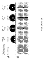
- FIG. 1(B) shows optical micrographs of silver wires printed on the modified or unmodified Canson tracing paper substrates using the reactive silver ink with a target resolution of 80 ⁇ m, according to one or more embodiments described herein.
- FIG. 2 shows an electroadhesive pad printed on C 10 F Canson tracing paper using the reactive silver ink.
- FIG. 2(A) shows a schematic of the interdigitated electrode design used for the pad with actual dimensions, according to one or more embodiments described herein.
- FIG. 2(B) shows an illustration of a cross-section of the electroadhesive pad depicting the fringe electric field lines, generated from the electrode, charging a glass surface by induction, according to one or more embodiments described herein.
- FIG. 2(C) shows a schematic of the arrangement of the electroadhesive pad used for the experiment, according to one or more embodiments described herein.
- FIG. 2(D) shows an electroadhesive pad (with dimensions given in FIG. 2(A) ) under an applied 2 kV potential adheres to a glass plate with sufficient strength to support a 500 g weight, according to one or more embodiments described herein.
- FIG. 3(A) left, shows a MEMS deflection sensor fabricated by depositing carbon ink on C 10 F Canson Vellum paper with an inkjet printer (Ercon 3456 silver ink was applied manually at the ends of the device to improve electrical connections with the testing rig), according to one or more embodiments described herein.
- FIG. 3(B) shows a schematic describing the experimental setup (left) and a diagram of the circuit employed for measuring device resistances (right), according to one or more embodiments described herein.
- FIG. 3(C) shows a plot of resistance vs. time for a representative device during 10 cycles of upward/downward deflection, according to one or more embodiments described herein.
- FIG. 4 shows the reproducibility of electrodes, printed on embossed omniphobic C 10 F Whatman paper using carbon ink, as characterized by cyclic voltammetry), according to one or more embodiments described herein.
- FIG. 4(A) shows a design of an electroanalytical device with a three-electrode system, according to one or more embodiments described herein, where the dotted line indicates that the embossed well is recessed into the surface and protrudes on the back side of the paper, according to one or more embodiments described herein.
- FIG. 4(B) shows an illustration of the electroanalytical device with a drop placed in the embossed well), according to one or more embodiments described herein.
- FIG. 4(A) shows a design of an electroanalytical device with a three-electrode system, according to one or more embodiments described herein, where the dotted line indicates that the embossed well is recessed into the surface and protrudes on the back side of the paper, according to one
- FIG. 4(C) shows a top view of an actual device with a 50- ⁇ L drop of an aqueous solution of an electroactive species added to the well, according to one or more embodiments described herein.
- FIG. 4(D) shows the side-view of the actual device in FIG. 4(C) , according to one or more embodiments described herein.
- FIG. 4(E) shows the cyclic voltammograms of 4-aminophenol (PAP) at concentrations of 1 mM (black) and 100 ⁇ M (grey) tested on seven different devices (D1-D7), i.e., potential measured vs. the quasi-reference electrode with a scan rate of 100 mV/s, according to one or more embodiments described herein.
- PAP 4-aminophenol
- FIG. 5 shows the relationship between the width of features printed on a modified or unmodified paper, and the contact angle of water on the respective surface, according to one or more embodiments described herein.
- FIG. 6 shows SEM images of the surfaces of silver features printed on treated and untreated papers using reactive silver ink, according to one or more embodiments described herein.
- FIG. 7 shows cross sectional imaging of printed wires, according to one or more embodiments described herein.
- FIG. 7 (left) shows SEM images of the cross-sections silver wires printed in three layers on C 10 F ( FIG. 7 , top) and untreated ( FIG. 7 , bottom) paper, using reactive silver ink, according to one or more embodiments described herein.
- the axis in each SEM image maps to the energy-dispersive X-ray (EDS) spectroscopy line scans ( FIG. 7 , right) collected for the Ag L line emission, according to one or more embodiments described herein.
- EDS energy-dispersive X-ray
- FIG. 8 shows the surface profilometry of patterned paper, according to one or more embodiments described herein.
- FIGS. 8(A) and 8(B) show 3-D profiles of 0.8 mm ⁇ 0.8 mm areas of omniphobic C 10 F paper, and untreated paper, respectively, patterned with wires printed with three layers of reactive silver ink, according to one or more embodiments described herein.
- FIG. 8(C) shows the single line scans across the surface of the wire illustrating the accumulation of silver on the surface of the C 10 F paper, according to one or more embodiments described herein.
- FIG. 8(D) shows the blurred boundary at the edge of the wire printed on untreated paper, according to one or more embodiments described herein.
- FIG. 10 shows the percentage change in resistance following exposure of wires printed on C 10 F omniphobic paper to solvent, according to one or more embodiments described herein.
- FIG. 11 shows the resistance to creasing of printed conductive features, according to one or more embodiments described herein.
- FIGS. 11(A) -(C) show images of the test specimens undergoing a creasing cycle according to one or more embodiments described herein.
- FIG. 11(D) shows that no significant increase in the respective electrical resistance was observed for the conductive prints relative to their initial, as-printed, state when the creasing occurs with the silver features either in compression ( FIG. 11(E) ) or in extension ( FIG. 11(F) ).
- a cellulosic substrate-based device including a cellulosic substrate comprising a functionalized portion, e.g., a portion of its surface, of the cellulosic substrate covalently functionalized by a chemical moiety in an amount sufficient to render the functionalized portion of the surface omniphobic or hydrophobic; and a material printed on the functionalized portion of the surface, wherein the printed material has a high resolution.
- the high resolution of the printed material is selected from a group consisting of a line edge roughness of less than about 15 ⁇ m, a lateral resolution of less than about 50 ⁇ m, and a combination thereof.
- the term “device,” as used herein, refers to any object made or adapted for one or more particular purpose or function.
- the device can be any mechanical or electronic equipment, such as a display, a sensor, a circuit board, or a diagnostic device, or a structural component (e.g., a surface) thereof.
- the cellulosic substrate is covalently functionalized by a chemical moiety to render the cellulosic substrate omniphobic or hydrophobic.
- chemical moieties include organosilanes, fluorinated hydrocarbons, chlorinated hydrocarbons, fluorinated chlorinated hydrocarbons (e.g., a hydrocarbon which has both F and Cl substitutions), and perfluorocarbon moieties.
- Other chemical moieties known in the art which have omniphobic or hydrophobic properties are contemplated.
- the paper or other cellulosic substrate is transformed into an omniphobic material by exposure to vapors of a fluorinated or perfluorocarbon containing species, e.g., fluoroalkyl trichlorosilane, which react with the hydroxyl groups of the cellulosic substrate to form fluorinated or perfluorocarbon chains of grafted siloxane molecules.
- a fluorinated or perfluorocarbon containing species e.g., fluoroalkyl trichlorosilane
- this process is a single-step, rapid (e.g., ⁇ 5 min to completion) and low-cost process.
- the combined effects of the fluorinated or perfluorocarbon chains of grafted siloxane molecules with the micro-scale roughness and porosity of paper or other cellulosic substrate yield an omniphobic material that preserves the properties of mechanical flexibility and low resistance to transport of gas of the untreated paper.
- the device described herein includes printed features with very high resolution. Without wishing to be bound by any particular theory, it is believed that the small line edge roughness and/or small line width of the printed material enables the printing of these small printed features in the micro scale.
- the high resolution of a printed feature can be reflected by the low line edge roughness and/or the high line lateral resolution of the material printed on the functionalized portion of the surface.
- line edge roughness is defined as the deviation of a feature edge (as viewed top-down) from a smooth, ideal shape—that is, the edge deviations of a feature that occur on a dimensional scale smaller than the resolution limit of the fabrication method that was used to print the feature.
- line edge roughness can be measured by the standard deviation of the edge position.
- the printed material has a line edge roughness of less than about 10 ⁇ m, 9 ⁇ m, 8 ⁇ m, 7 ⁇ m, 6 ⁇ m, 5 ⁇ m, 4 ⁇ m, 3 ⁇ m, 2 ⁇ m, or 1 ⁇ m, or in a range bound by any two values disclosed herein. In some specific embodiments, the printed material has a line edge roughness from about 10 ⁇ m-1 ⁇ m, 8 ⁇ m-1 ⁇ m, 6 ⁇ m-1 ⁇ m, 5 ⁇ m-1 ⁇ m, 3 ⁇ m-1 ⁇ m, 2 ⁇ m-1 ⁇ m, 10 ⁇ m-5 ⁇ m, 6 ⁇ m-2, or 4 ⁇ m-2 ⁇ m.
- the term “line lateral resolution” is defined as the average width of a line measured in the direction perpendicular to the long axis of the line and coincident with the 2D plain of the sheet of the cellulosic substrate, e.g., paper.
- other shapes of features e.g., circles, triangles, and ellipses, are printed on the paper.
- “radial resolution” is used for cases when circles are printed on a cellulosic substrate, e.g., paper, which is defined as the resolution of the diameter of the circle, triangles, or ellipses.
- At least a portion of the material printed on the functionalized portion of the surface has a high line lateral resolution or radial resolution less than about 300 ⁇ m, 200 ⁇ m, 100 ⁇ m, 50 ⁇ m, 40 ⁇ m, 30 ⁇ m, 25 ⁇ m, 20 ⁇ m, 15 ⁇ m, 10 ⁇ m, 5 ⁇ m, 2 ⁇ m, 1 ⁇ m, 500 nm, 200 nm, 100 nm, or in the range of 100 nm to 50 ⁇ m, or any other range bounded by any of the values noted here.
- the ink printed builds up on the surface of the sheet of cellulosic substrate instead of wicking into it.
- the print depth resolution in these embodiments, can be defined as the distance of penetration of ink into a sheet of paper measured as the average distance of ink penetration below the 2D planar surface of a sheet of paper. The distance can be any distance that is less than the penetration that would occur due to wicking of ink into a sheet of unmodified hydrophilic paper.
- cellulosic substrate includes cellulose and other cellulosic substrate known in the art.
- a cellulosic substrate includes articles of manufacture such as paper and cardboard that are made primarily of cellulose. It also includes modified cellulose, for example, where the hydroxyl groups of cellulose can be partially or fully reacted with various reagents to afford derivatives with useful properties such as nitrocellulose, cellulose esters and cellulose ethers.
- Non-limiting examples of the cellulosic substrate include paper, cellulose derivatives, woven cellulosic materials, and non-woven cellulosic materials.
- At least a portion of the cellulosic substrate is covalently functionalized.
- the whole surface of the cellulosic substrate is covalently functionalized.
- at least the portion of the fibers of the cellulosic substrate is covalently functionalized.
- the fibers of a paper pulp are covalently modified and paper sheet is subsequently formed using the modified pulp.
- the whole surface of the cellulosic substrate is covalently functionalized.
- the whole thickness of the cellulosic substrate, e.g., paper is covalently functionalized.
- a wet chemical processing step on the cellulose pulp can be carried out to modify the pulp using one or more chemicals described herein before turning that pulp into paper sheets.
- the cellulosic substrate is flexible.
- the cellulosic substrate can be bent through its thinnest dimension, rolled around a cylindrical rod with a diameter, and return to a flat configuration without damaging the integrity of the substrate. Due to this flexibility, paper devices fabricated from the cellulosic substrate can be treated in this fashion without damaging the integrity and/or functionality of the resultant folded device.
- the cellulosic substrate can be folded, creased, or otherwise mechanically shaped to impart structure and function to a device formed from the cellulosic substrate.
- the cellulosic substrate is paper.
- Paper is inexpensive, widely available, readily patterned, thin, lightweight, and can be disposed of with minimal environmental impact. Furthermore, a variety of grades of paper are available, permitting the selection of a paper substrate with the weight (i.e., grammage), thickness and/or rigidity and surface characteristics (i.e., chemical reactivity, hydrophobicity, and/or roughness) desired for the fabrication of a particular microfluidic device, a display, a battery, and a sensor.
- weight i.e., grammage
- thickness and/or rigidity and surface characteristics i.e., chemical reactivity, hydrophobicity, and/or roughness
- Suitable papers include, but are not limited to, chromatography paper, card stock, filter paper, vellum paper, printing paper, wrapping paper, ledger paper, bank paper, bond paper, blotting paper, drawing paper, fish paper, tissue paper, paper towel, wax paper, and photography paper.
- the paper is cardstock paper, which is particularly suitable as the cellulosic material is lightweight and flexible, sufficiently smooth to create a tight seal with tape and inexpensive; it is also thick enough (300 ⁇ m) to retain mechanical stability while accommodating folds and creases introduced during the forming process. Thinner, more flexible paper can be used when more complex or more highly folded and/or creased structures are desired.
- the cellulosic substrate is paper having a grammage, expressed in terms of grams per square meter (g/m 2 ), of greater than 30, 40, 50, 60, 70, 75, 85, 100, 125, 150, 175, 200, 225, or 250, or in any range bounded by any two values disclosed herein.
- the cellulosic substrates can be covalently modified to provide an omniphobic or hydrophobic surface using any suitable synthetic methodology.
- hydroxyl groups present on the surface of the cellulosic substrate may be covalently functionalized by silanization, acylation, or by epoxide, aziridine, or thiirane ring opening.
- the cellulosic substrate is treated with a volatile reagent to increase its oleophobicity and/or hydrophobocity.
- examples of suitable chemical functional groups include linear, branched, or cyclic perfluoro or fluoroalkyl groups; linear, branched, or cyclic perfluorinated or fluorinated alkenyl groups; linear, branched, or cyclic perfluorinated or fluorinated alkynyl groups, aryl groups, optionally substituted with between one and five substituents individually selected from the group consisting of alkyl, alkoxy, amino, halogen, nitrile, CF 3 , ester, amide, aryl, and heteroaryl.
- the omniphobic group is an aryl ring substituted with fluorine atoms and/or trifluoromethyl groups, or a linear or branched alkyl group substituted with one or more halogen atoms.
- the introduction of halogenated functional groups via glycosidic linkages increases the omniphobicity of the cellulosic surface.
- examples of suitable hydrophobic or omniphobic groups include linear, branched, or cyclic alkyl groups; linear, branched, or cyclic alkenyl groups; linear, branched, or cyclic alkynyl groups, aryl groups, heteroaryl groups, optionally substituted with between one and five substituents individually selected from alkyl, alkoxy, amino, halogen, nitrile, CF 3 , ester, amide, aryl, and heteroaryl.
- the hydrophobic group may also be a fluorinated or perfluorinated analog of any of the groups described above.
- the chemical moiety is linked to the cellulosic surface through a siloxane linker.
- the surface hydroxyl groups of the cellulosic substrate e.g., the cellulose fibers
- Suitable silanes include linear or branched fluoroalkyl or perfluoroalkyl trihalosilanes, and fluoroalkyl or perfluoroalkyl aminosilanes.
- the chemical moiety is R (n1) SiCl (n2) —, wherein n1 is 1, 2, or 3; n2 is 0, 1, or 2; and the sum of n1 and n2 is 3.
- R H represents any optionally substituted straight or branched C 1 -C 30 alkyl, C 1 -C 30 cycloalkyl, C 1 -C 30 alkenyl, or C 1 -C 30 alkynyl.
- R F represents any optionally substituted straight or branched, fluorinated or perfluorinated C 1 -C 30 alkyl, C 1 -C 30 cycloalkyl, C 1 -C 30 alkenyl, or C 1 -C 30 alkynyl, with one or more fluoro substitutions. In certain embodiments, R F can also have one or more Cl substitutions.
- R C1 represents any optionally substituted straight or branched chlorinated C 1 -C 30 alkyl, C 1 -C 30 cycloalkyl, C 1 -C 30 alkenyl, or C 1 -C 30 alkynyl, with one or more chloro substitutions.
- R Cl can also have one or more F substitutions.
- the chemical moiety is R H SiCl 2 —, R F SiCl 2 —, or R Cl SiCl 2 —.
- a fluorinated hydrocarbon or perfluorocarbon moiety is grafted to the cellulose fiber when a fluorinated or perfluorinated hydrocarbon silyl chloride's chlorosilane part of the compound reacts with a hydroxyl group on the cellulose to form a covalent bond between the two moieties.
- the cellulosic substrate is reacted with one or more fluoroalkyl or perfluoroalkyl trichlorosilanes, such as (tridecafluoro-1,1,2,2-tetrahydrooctyl) trichlorosilane, to form a fluorinated, highly textured, omniphobic surface on the cellulosic substrate.
- the surface groups may have all or a portion of the hydrogen atoms replaced by fluorine atoms.
- the surface free energy of the solid can be lowered sufficiently to render it omniphobic.
- Other functional groups can be present, but high surface energy functional groups (OH, C ⁇ O, etc.) may be incompatible for stability reasons and their presence should be limited.
- the chemical moiety is one or more chemical moieties selected from the group consisting of: (3,3,4,4,5,5,6,6, 7,7,8,8,9,9,10,10,10-heptadecafluorodecyl) dichlorosilyl-, CF 3 —(CF 2 ) 7 —CH 2 —CH 2 —SiCl 2 —(C 10 F ), decyl trichlorosilane, CH 3 (CH 2 ) 9 SiCl 2 —(C 10 H), and CH 3 SiCl 2 —.
- the silanization treatment does not degrade the physical properties of the paper and does not require pre- or post-treatment steps (e.g., washing to remove reagents or side products, drying, etc.).
- the paper can be silanized before or after forming the device into its final form, e.g., by folding and creasing. Silanizing after folding can avoid damaging the organosilane layer or exposing cellulose fibers that had not come in contact with vapors of organosilane; however, the more complex surfaces may be more difficult to obtain complete coverage.
- the covalently modified omniphobic cellulosic substrate (prior to introduction of a low surface tension perfluorinated liquid) is substantially impermeable to aqueous solutions.
- the covalently modified cellulosic substrate has a contact angle with water, as measured using a goniometer, of more than 90° (i.e., it is hydrophobic).
- the covalently modified cellulosic substrate has a contact angle with water of more than about 95°, 100°, 105°, 110°, 115°, 120°, 125°, 130°, 135°, 140°, 145°, 150°, or 155° or in the range of 95° to 155° or any other range bounded by any of the values noted here.
- An omniphobic surface exhibits contact angles higher than 90° with both water and hexadecane.
- Covalent attachment of the modifying reagent to the cellulosic substrate can be confirmed using appropriate molecular and surface analysis methods, including reflectance FTIR and XPS.
- at least 5%, more preferably at least 25%, more preferably at least 35%, more preferably at least 50%, most preferably at least 75% of the pendant —OH groups present on the cellulosic backbone are covalently modified.
- more than 80% of the pendant —OH groups present on the cellulosic backbone are covalently modified.
- the material can be printed onto the functionalized surface by ink jet printing.
- ink jet printing other printing methods known in the art, such as gravure, screen printing, stencil printing, offset printing, and flexography can be used.
- the device described herein is prepared by printing the material in a liquid onto the functionalized surface portion.
- the material include conductive metal, carbon, dielectric material, conductive polymers, materials for printing LEDs, ink, dye, nanoparticles, proteins, cells, buffers, electrolytes, chemicals for colorimetric assays, materials for printing transistors, materials for printing batteries, materials for printing explosive sensors, materials for printing narcotics sensors, materials for printing chemical and biological weapons sensors, and any combination thereof.
- the material can be dissolved in the liquid to form a printing solution.
- the material e.g., nanoparticles, proteins, or cells with sizes similar to the printed features
- the liquid used herein can be hydrophobic or hydrophilic.
- One non-limiting feature of the device as disclosed herein is the greatly improved chemical resistance.
- the common hydrophobic or hydrophilic liquid known in the art can be used as medium to deliver the material.
- material is a conductive metal, carbon, dielectric material, cells, conductive polymers, proteins, dye compounds (for example oxygen sensing dyes) and materials for printing LEDs such as the compounds used in OLEDs.
- the material printed on the functionalized surface is a part of a circuit wire, sensor, electrode, resistor, transistor, antenna, capacitor, or inductor deposited on the functionalized surface.
- the device is resistant to hydrophobic chemicals or both hydrophobic and hydrophilic chemicals.
- the device can be exposed to water, ethanol, glycerin, toluene, glacial acetic acid, chloroform, dimethyl sulfoxide, acetone, hexadecane, or other hydrophobic or hydrophilic chemicals, without losing any significant amount of the printed material's mass.
- water ethanol, glycerin, toluene, glacial acetic acid, chloroform, dimethyl sulfoxide, acetone, hexadecane, or other hydrophobic or hydrophilic chemicals
- the device can be exposed to water, ethanol, glycerin, toluene, glacial acetic acid, chloroform, dimethyl sulfoxide, acetone, hexadecane, or other hydrophobic or hydrophilic chemicals, without causing the paper to swell, decompose, or dissolve when exposed to solvent thereby protecting the integrity of the printed device.
- the material printed on the functionalized surface has an increase of resistance of less than about 10%, 9%, 8%, 7%, 6%, 5%, 4%, 3%, 2%, or 1% or in the range of 1% to 10%, or any other range bounded by any of the values noted here after the printed material is exposed to the hydrophobic or hydrophilic chemical.
- the material printed on the functionalized surface has virtually no increase of resistance when exposed to water or glycerin (a change in resistance of ⁇ 0% on average).
- the material printed on the functionalized surface has an average increase of resistance of about 5% when exposed to toluene and/or acetone.
- the material printed on the functionalized surface forms a capacitor, an inductor, a LED, or a battery.
- the capacitor printed on the functionalized surface has a change of capacitance (e.g., loss of capacitance) of less than about 10%, 9%, 8%, 7%, 6%, 5%, 4%, 3%, 2%, or 1% or in the range of 1% to 10%, or any other range bounded by any of the values noted here after the printed material is exposed to the hydrophobic or hydrophilic chemical.
- the inductor printed on the functionalized surface has a change of inductance (e.g., loss of inductance) of less than about 10%, 9%, 8%, 7%, 6%, 5%, 4%, 3%, 2%, or 1% or in the range of 1% to 10%, or any other range bounded by any of the values noted here after the printed material is exposed to the hydrophobic or hydrophilic chemical.
- a change of inductance e.g., loss of inductance
- the LED printed on the functionalized surface has a loss of luminosity of less than about 10%, 9%, 8%, 7%, 6%, 5%, 4%, 3%, 2%, or 1% or in the range of 1% to 10%, or any other range bounded by any of the values noted here after the printed material is exposed to the hydrophobic or hydrophilic chemical.
- the battery printed on the functionalized surface has a loss of energy storage capacity of less than about 10%, 9%, 8%, 7%, 6%, 5%, 4%, 3%, 2%, or 1% or in the range of 1% to 10%, or any other range bounded by any of the values noted here after the printed material is exposed to the hydrophobic or hydrophilic chemical.
- the material printed on the functionalized surface has surprisingly good adhesion to the functionalized surface.
- the strength of the adhesion of the material to the functionalized surface can be measured or demonstrated by using an adhesive tape test.
- an adhesive tape e.g., Scotch matte finish magic tape, 3M
- the adhesive tape is subsequently removed and the loss of the material mass on the functionalized surface can be measured.
- the loss of the material mass on the functionalized surface can be measured or calculated, e.g., with a digital multimeter, by measuring the change in resistance following the removal of each application of tape as a proxy for the loss of material mass.
- the material printed on the functionalized surface loses less than about 10%, 9%, 8%, 7%, 6%, 5%, 4%, 3%, 2%, or 1%, or in the range of 1% to 10%, or any other range bounded by any of the values noted here of its mass after an adhesive tape is applied onto the printed material and subsequently removed.
- the material printed on the functionalized surface has an increase resistance of less than about 10%, 9%, 8%, 7%, 6%, 5%, 4%, 3%, 2%, or 1%, or in the range of 1% to 10%, or any other range bounded by any of the values noted here of its mass after an adhesive tape is applied onto the printed material and subsequently removed.
- the device described herein has excellent foldability and flexibility.
- the material printed on the functionalized surface has a resistance increase of less than about 10%, 9%, 8%, 7%, 6%, 5%, 4%, 3%, 2%, or 1%, or in the range of 1% to 10%, or any other range bounded by any of the values noted here.
- the printed material and the functionalized surface on which the material is printed are folded more than 100, 90, 80, 70, 60, 50, 40, 30, 20, 10, or 5 times without significant increase of resistance (e.g., less than about 10%, 9%, 8%, 7%, 6%, 5%, 4%, 3%, 2%, or 1%, or in the range of 1% to 10%, or any other range bounded by any of the values noted here).
- the printed material and the functionalized surface on which the material is printed can be folded in a way so that the printed material is compressed (e.g., FIG. 11(E) ) or extended (e.g., FIG.
- the material, e.g., conductive traces, printed on the functionalized surface can be incorporated into a variety of devices.
- the device is a diagnostic device configured to detect an analyte through any suitable chemical or physical signals corresponding to the presence of the analyte.
- the analyte is selected from the group consisting of small molecules, proteins, lipids, polysaccharides, nucleic acids, prokaryotic cells, eukaryotic cells, particles, viruses, metal ions, narcotics, chemical weapons, biological weapons, explosives and explosive precursors (e.g. the chemicals used to make explosives or chemical intermediates that are generated when making explosives), and any combination thereof.
- the analyte is selected from the group consisting of glucose, creatine, 4-amino-phenol, red blood cells, lipids, creatinine, urea, albumin, bilirubin, aspartate transaminase, alanine transaminase, alkaline phosphatase, antibodies, and any combination thereof.
- the device as described herein can be a display, an antenna, a temperature sensor, pressure sensor, humidity sensor, volatile organic chemical sensor, a force sensor, a sensor for an ELISA or other immunoassays, MEMS, an electroadhesive pad, RFID tag, a battery, resistor, capacitor, transistor, LED, OLED, or a logic gate.
- the material printed onto the functionalized surface is the strain limiting layer of a soft robot.
- the functionalized cellulosic substrate can be the strain limiting layer of the soft robot with embedded electronics printed on it.
- Strain is a description of deformation in terms of relative displacement of a body.
- a deformation results from a stress induced by applied forces, in the case here, for example, by the pressurizing force. Because materials of lower stiffness or smaller elastic modulus will deform to a greater degree than the higher elastic modulus materials, the low stiffness materials experience strain or deformation first. As a result, the strain in the material of higher stiffness or greater elastic modulus is smaller or “limited.”
- the layer or wall of the soft robot that is stiffer, e.g., has a higher elastic modulus is referred herein to as the “strain limiting” layer or wall or membrane.
- the cellulosic substrate-based device including the material printed on the functionalized flexible surface can act as the strain limiting layer of the robot.
- soft robots are built with a strain limiting layer made of the functionalized paper or other cellulosic substrate described herein with wires printed on its surface as this strain limiting layer.
- the functionalized paper or other cellulosic substrate could not only be used as a structural component of the soft actuator but also as a means of distributing electricity to components embedded in the soft actuator like motors or sensors. Further description of the soft robot can be found in WO 2012148472, the content of which is hereby incorporated by reference.
- the device described herein is an electrode adhesion device.
- the material printed on the functionalized surface includes interdigitated positive and negative electrodes opposing each other.
- Electroadhesion is an electrically controlled adhesion technology used for applications that require reversible, adhesive-free, binding to a substrate.
- a typical electroadhesion pad consists of two interdigitated electrodes patterned on the surface of a dielectric material. Electrostatic forces are created between electroadhesive pads and a substrate that is either electrically insulating or conductive (although much lower forces are achieved with electroadhesion for nonconducting objects). Charging the interdigitated electrode creates fringe field lines between the positive and negative electrodes that extend in the direction normal to the electrode pattern.
- the electroadhesive pad When the electroadhesive pad is brought in proximity to a substrate (e.g., glass, drywall, wood, concrete, or metals), its fringe-field lines penetrate the substrate, and redistribute charge to create a pattern of opposite polarity in the substrate.
- a substrate e.g., glass, drywall, wood, concrete, or metals
- the Coulombic attraction between the charges on the electrode and the complementary, induced charges on the surface of the substrate creates an electrostatic force that can be used to adhere the electroadhesive pad to the substrate. Controlling of the electrostatic adhesion voltage permits the adhesion to be turned on and off easily.
- the material deposited onto the surface of the functionalized cellulosic substrate includes a pair of interdigitated electrodes (e.g., FIG. 2 ).
- FIG. 2(A) shows a schematic of the interdigitated electrode design used for the pad with actual dimensions.
- FIG. 2(B) shows an illustration of a cross-section of the electroadhesive pad depicting the fringe electric field lines, generated from the electrode, charging a glass surface by induction.
- FIG. 2(C) shows a schematic of the arrangement of the electroadhesive pad used for the experiment.
- FIG. 2(D) shows an electroadhesive pad (with dimensions given in FIG.
- electroadhesion is sufficient to support a 10,000 kg, 1000 kg, 500 kg, 100 kg, 1000 g, 900 g, 700, or 500 g weight hanging from the base of the sheet. Heavier or lighter weights are contemplated. Without wishing to be bound by any particular theory, it is believed that the amount of weight that the substrate can support depends on many factors including the density of wires in the electrode, the overall size of the electrode, the operating voltage and the material that the device is adhering to.
- a method of making a paper-based device comprising: covalently functionalizing at least a portion of the surface of a cellulosic substrate by a chemical moiety in an amount sufficient to render the functionalized surface omniphobic or hydrophobic; and printing a material on the functionalized surface, wherein the printed material has a line edge roughness of less than about 15 ⁇ m and/or a line lateral resolution of less than about 50 ⁇ m.
- the cellulosic substrate can be paper, cellulose derivatives, woven cellulosic materials, or non-woven cellulosic materials.
- the functionalized surface comprises a fluorinated hydrocarbon group, chlorinated hydrocarbon group, or hydrocarbon group linked to the cellulosic surface through a siloxane linker.
- the chemical moiety is selected from the group consisting of CF 3 (CF 2 ) 7 CH 2 CH 2 SiCl 3 and CH 3 SiCl 3 . Any suitable chemical moieties described herein can be used.
- the printed material may have a line edge roughness of less than about 100 ⁇ m, 50 ⁇ m, 30 ⁇ m, 20 ⁇ m, 15 ⁇ m, 10 ⁇ m, 9 ⁇ m, 8 ⁇ m, 7 ⁇ m, 6 ⁇ m, 5 ⁇ m, 4 ⁇ m, 3 ⁇ m, 2 ⁇ m, or 1 ⁇ m.
- At least a portion of the material printed on the functionalized surface has a width of less than about 500 ⁇ m, 400 ⁇ m, 300 ⁇ m, 250 ⁇ m, 200 ⁇ m, 150 ⁇ m, 100 ⁇ m, 50 ⁇ m, 40 ⁇ m, 30 ⁇ m, 25 ⁇ m, 20 ⁇ m, 15 ⁇ m, 10 ⁇ m, 5 ⁇ m, 2 ⁇ m, or 1 ⁇ m.
- the material is printed on the functionalized surface by ink-jet printing or any other printing method known in the art.
- the material is printed on the functionalized surface by printing on a material solution or dispersion in a liquid.
- the material may be a conductive metal, carbon, dielectric material, conductive polymers, proteins, dye compounds (for example oxygen sensing dyes) and materials for printing LEDs like the compounds used in OLEDs or cells.
- a method of using the device described herein to detect an analyte includes: providing the cellulosic substrate-based device of any one of the embodiments described herein; contacting the cellulosic substrate-based device with a sample potentially containing the analyte; and determining the presence or absence of a chemical or physical signal corresponding to the presence of the analyte.
- the analyte is selected from the group consisting of small molecules, proteins, lipids, polysaccharides, nucleic acids, prokaryotic cells, eukaryotic cells, particles, viruses, metal ions, and combination thereof.
- paper devices are prepared using a cellulosic substrate that has been covalently modified to increase its hydrophobicity and/or omniphobicity.
- the cellulosic substrate can be covalently modified using any suitable methodology, as discussed below.
- Cellulose is a polysaccharide including a linear chain of several hundred to over ten thousand ⁇ (1 ⁇ 4) linked D-glucose units. Cellulose is mainly used to produce paperboard and paper.
- a cellulosic substrate includes articles of manufacture such as paper and cardboard that are made primarily of cellulose. It also includes modified cellulose, for example where the hydroxyl groups of cellulose can be partially or fully reacted with various reagents to afford derivatives with useful properties such as nitrocellulose, cellulose esters and cellulose ethers.
- the functionalized cellulosic substrate further include one or more hydrophilic microfluidic channels.
- Such microfluidic channels can be open channels. Open channels are conduits that contain a central void space through which fluid flows, and a bottom and side-walls formed from a cellulosic substrate that has been covalently modified to increase its hydrophobicity, such that the bottom and side-walls of the open channel are substantially impermeable to the fluid flowing through the open channel. Further details of the microfluidic channels can be found in PCT/US2013/43882, the content of which is incorporated by reference.
- all or some of the surface hydroxyl groups of the cellulosic substrate are acylated by reaction, for example, with one or more perfluoro or fluoroalkyl groups functionalized with an acid chloride.
- the cellulosic substrate can also be covalently modified by treatment with a hydrophobic group substituted with one or more epoxide or thiirane rings.
- the omniphobicity/oleophilicity of the covalently modified cellulosic substrate can be quantitatively assessed by measuring the contact angle of a water droplet on the substrate surface using a goniometer.
- the omniphobicity/oleophilicity of the covalently modified cellulosic substrate can be qualitatively assessed by rolling droplets of water and/or hexane on the surface of the modified paper to evaluate the wettability of the surface.
- R F paper omniphobic and/or hydrophobic “fluoroalkylated paper”
- R F paper omniphobic and/or hydrophobic “fluoroalkylated paper”
- the omniphobic paper is used as a substrate for the deposition of multiple inks using a piezoelectric inkjet printer.
- Piezoelectric inkjet printing is a non-contact printing method that does not require the generation of a master, but instead creates patterns based on easily modifiable digital files. The precise control over the positioning of the droplets and over the interfacial free energy of the paper substrate enabled us to print, with high resolution, conductive patterns that are resistant to damage from exposure to common solvents and to folding.
- a method to produce a flexible circuit or circuit board on the omniphobic or hydrophobic substrate disclosed herein is described.
- one or more conventional electronic components can be mounted to the surface of the printed circuit board.
- these conventional electronic components include conventional resisters, capacitors, microcontrollers, wireless transmitters, wireless receivers, inertial monitoring units, transistors, zener diodes, batteries, strain sensors, force sensors, chemical sensors, LEDs.
- all components for one or more circuit board are fabricated by printing methods.
- the surface free energy of paper was modified using a fast vapor-phase treatment with organosilanes. This process, which occurs in approximately five minutes, does not require wetting (and distorting) the paper, or removal of solvents.
- Treatment with non-fluorinated organosilanes renders paper hydrophobic; treatment with highly fluorinated compounds such as fluoroalkyltrichlorosilanes transforms paper into a material that is omniphobic (both hydrophobic and oleophobic).
- the chemical modifications result in engineered papers with mechanical properties independent of humidity. These engineered papers still retain the flexibility and low resistance to gas transport of untreated paper.
- FIG. 1B shows the actual wicking of the treated or untreated papers, corresponding to the picture above.
- the target resolution of 80 ⁇ m shown in FIG. 1B is the width of the line as represented in the digital file from which the physical print is generated.
- FIG. 1 clearly demonstrates that the wetting of untreated and silanized paper by water correlates with the lateral resolution of the printed conductive features.
- Canson tracing paper, untreated or silanized with TDA, C 1 H , C 10 H , and C 10 F is used as a substrate for the inkjet printing of 80- ⁇ m-wide wires (the intended width based on the features in the digital file) using reactive silver ink dispensed by a Fuji Dimatix DMP-2831 printer. More details of reactive silver ink can be found in S. B. Walker, J. A. Lewis, J. Am. Chem. Soc. 2012, 134, 1419, which is incorporated by reference.
- the reactive silver ink is essentially a modified Tollens' reagent: that is, an aqueous solution that contains a soluble complex of silver ions, primary amines and a reducing agent—formic acid.
- Tollens' reagent that is, an aqueous solution that contains a soluble complex of silver ions, primary amines and a reducing agent—formic acid.
- the chelating primary amines are volatilized upon heating at modest temperatures ( ⁇ 120° C.), the formic acid reduces the uncomplexed silver ions to silver particles.
- the wires had an intended width (based on the size of the features in the digital file) of 300 ⁇ m.
- the treated paper the layers of ink were stacked up on top of the paper to give a thick metal feature. This is in contrast to the untreated paper where the ink wicked into the paper based on the distribution of ink.
- the axis in each SEM image maps to the energy-dispersive X-ray (EDS) spectroscopy line scans ( FIG. 7 , right) collected for the Ag L line emission.
- the red dots overlayed with the SEM images indicate the location of the red vertical lines in the EDS plots, representing the approximate edge of the paper.
- FIGS. 8(A) and 8(B) show 3-D profiles of 0.8 mm ⁇ 0.8 mm areas of omniphobic C 10 F paper, and untreated paper, respectively, patterned with wires printed with three layers of reactive silver ink. Single line scans across the surface of the wire shows in FIG. 8(C) the accumulation of silver on the surface of the C 10 F paper, and in FIG. 8(D) the blurred boundary at the edge of the wire printed on untreated paper.
- the observed conductivity of wires printed on silanized papers stands in contrast with the very high resistance of the features printed on untreated paper (resistance greater than the detection limit of our multimeter>10 M ⁇ ).
- inkjet-printed patterns is limited by several factors: the wettability of the substrate, the hydrodynamics of the jetted microdroplets, and the volatility of the constituents of the ink.
- 20 ⁇ m is considered the smallest feature size achievable via inkjet printing.
- Features of this size are typically achieved using 1-pL droplets, but can also be achieved by tuning the waveform of 10-pL cartridges to achieve droplet volumes below 10 pL.
- a 10-pL spherical droplet has a diameter of 27 ⁇ m.
- SEM imaging ( FIG. 9 ) shows that a maximum lateral resolution of 28 ⁇ 5 ⁇ m and a line edge roughness of 6 ⁇ m is achieved on this paper. To the best of our knowledge, this resolution has never before been achieved with droplets of this volume, suggesting that a high level of control over line width can be achieved by decreasing the surface free energy of the substrate.
- the 28 ⁇ m-wide feature appears to be continuous by SEM, it is not conductive.
- wires were printed (25 cm long, and 120 ⁇ m wide, printed with 5 layers of ink) using silver nanoparticle-, reactive silver-, and carbon-based inks onto a series of “alkylated papers” (“R H paper” produced by vapor-phase silanization of paper with alkyl trichlorosilanes), “fluoroalkylated papers” (“R F paper” produced by vapor-phase silanization of paper with fluoroalkyl trichlorosilanes), and PET films, and tested their resistance.
- R H paper produced by vapor-phase silanization of paper with alkyl trichlorosilanes
- R F paper fluoroalkylated papers
- PET films and tested their resistance.
- wires printed on C 10 F and C 1 H treated paper have resistances comparable to wires printed on a commercial PET film designed for conductive inkjet printing (See Table 1).
- FIGS. 11(A) -(C) Images of these samples undergoing a creasing cycle are shown in FIGS. 11(A) -(C).
- a crosshead distance of 0 mm leads to the formation of a crease in the paper substrate in the direction perpendicular to the printed silver features.
- FIG. 11(D) shows that no significant increase in the respective electrical resistance was observed for the conductive prints relative to their initial, as-printed, state when the creasing occurs with the silver features either in compression ( FIG. 11(E) ) or in extension ( FIG. 11(F) ).
- FIG. 11(E) initial, as-printed, state when the creasing occurs with the silver features either in compression
- FIG. 11(F) in extension
- 11(D) shows the averaged resistance values obtained from the array as a function of the number of creasing cycles.
- the resistance of the features did not vary significantly ( ⁇ 5%) from the original, pre-creasing resistance, after being folded once to either a +180° or a ⁇ 180° angle. This observation remains true for 100 consecutive folds, i.e., there is no significant increase ( ⁇ 5%) in the respective electrical resistance of the prints relative to their initial pre-creased values. It is hypothesized that the resilience of the wires to repeated cycles of folding is due, in part, to the strength of adhesion of the silver to the cellulose fibers of the C 10 F paper.
- Electroadhesion is an electrically controlled adhesion technology used for applications that require reversible, adhesive-free, binding to a substrate.
- a typical electroadhesion pad consists of two interdigitated electrodes patterned on the surface of a dielectric material. Electrostatic forces are created between electroadhesive pads and a substrate that is either electrically insulating or conductive (although much lower forces are achieved with electroadhesion for nonconducting objects).
- Charging the interdigitated electrode creates fringe field lines between the positive and negative electrodes that extend in the direction normal to the electrode pattern.
- a substrate e.g., glass, drywall, wood, concrete, or metals
- its fringe-field lines penetrate the substrate, and redistribute charge to create a pattern of opposite polarity in the substrate.
- the Coulombic attraction between the charges on the electrode and the complementary, induced charges on the surface of the substrate creates an electrostatic force that can be used to adhere the electroadhesive pad to the substrate. Controlling of the electrostatic adhesion voltage permits the adhesion to be turned on and off easily.
- Inkjet printing of the reactive silver ink was used to deposit a pair of interdigitated electrodes on a flexible dielectric layer (C 10 F -treated Canson tracing paper), in order to fabricate an electroadhesive device ( FIG. 2 ).
- the high resolution of the printing in conjunction with the use of omniphobic paper allowed us to deposit 500- ⁇ m wide interdigitated electrodes over a large area (57.5 cm 2 ).
- This high resolution of printing resulted in a pattern that was free of defects that give rise to short circuits, which, if present, would render the device inoperable.
- a potential difference of 2 kV was applied by connecting the electrodes to a high voltage power supply, and subsequently observed adhesion of the device to a glass surface that was sufficient to support a 500-g weight hanging from the base of the sheet.
- Cantilever-type MEMS deflection sensors were fabricated by depositing carbon ink (Methode 3801) on C 10 F -treated Canson Vellum paper.
- Canson Vellum paper (Model No. 702-442) is used as a substrate for the printing of MEMS cantilever deflection sensors, because it has a higher bending elastic modulus than many other papers.
- An image and a schematic of the testing rig are shown in FIGS. 3A (right) and 3 B respectively. The plot in FIG.
- 3C shows the resistance as a function of time of a typical device, as it is deflected cyclically. It was observed that a drop in resistance upon compression of the ink during upward deflection, reflected an increase in the number of connections in the percolation network between carbon particles. A rise in resistance is observed during downward deflection as a result of a corresponding decrease in the number of connections upon extension.
- Inkjet printing was used to deposit arrays of electrodes over a non-planar paper surface consisting of wells embossed in omniphobic C 10 F paper.
- Whatman #1 Chromatography Paper is used as a substrate for the printing of electrodes in electrochemical devices, because its high surface roughness increased the surface area accessible for electrochemical reactions and, for some applications, the sensitivity of detection.
- the electrode configuration consists of inkjet-printed working, counter, and quasi-reference carbon electrodes (WE, CE, and QRE, respectively).
- WE, CE, and QRE quasi-reference carbon electrodes
- FIG. 4 shows the reproducibility of electrodes, printed on embossed omniphobic C 10 F Whatman paper using carbon ink, as characterized by cyclic voltammetry), according to one or more embodiments described herein.
- FIG. 4(A) shows a design of an electroanalytical device with a three-electrode system where the dotted line indicates that the embossed well is recessed into the surface and protrudes on the back side of the paper.
- FIG. 4(B) shows an illustration of the electroanalytical device with a drop placed in the embossed well.
- FIG. 4(C) shows a top view of an actual device with a 50- ⁇ L drop of an aqueous solution of an electroactive species added to the well.
- FIG. 4(A) shows a design of an electroanalytical device with a three-electrode system where the dotted line indicates that the embossed well is recessed into the surface and protrudes on the back side of the paper.
- FIG. 4(D) shows the side-view of the actual device in FIG. 4(C) .
- FIG. 4(E) shows the cyclic voltammograms of 4-aminophenol (PAP) at concentrations of 1 mM (black) and 100 ⁇ M (grey) tested on seven different devices (D1-D7), i.e., potential measured vs. the quasi-reference electrode with a scan rate of 100 mV/s.
- the electrochemical operation of the paper-based three-electrode system is tested by recording cyclic voltammograms for 1 mM and 100 ⁇ M solutions of 4-amino-phenol ( FIG. 4E ).
- the silanizing reagents tris(dimethylamino)silane (TDAS), trichloromethylsilane (CH 3 SiCl 3 , “C 1 H ”), trichlorodecylsilane (CH 3 (CH 2 ) 9 SiCl 3 , “C 10 H ”), trichloro(3,3,4,4,5,5,6,6,7,7,8,8,9,9,10,10,10-heptadecafluorodecyl)silane (CF 3 (CF 2 ) 7 CH 2 —CH 2 SiCl 3 , “C 10 F ”), were purchased from Gelest Inc (Morrisville, Pa.). All chemicals were used as received without further purification.
- Canson tracing paper, Model No. 702-321, and Canson Vellum paper, Model No. 702-442 were purchased from Magnolia Art (Cambridge, Mass., USA) and used as received.
- Whatman #1 Chromatography Paper was purchased from GE Healthcare (N.J., USA) and used as received.
- the silanization reaction was conducted in a chamber with a volume of 0.01 m 3 at a temperature set at 105° C.
- the silanizing reagent was transferred into a glass vial and placed inside the chamber together with the samples.
- Each experiment typically required ⁇ 100 mg of silane in 5 mL of anhydrous toluene.
- the silane was vaporized at 105° C. under reduced pressure ( ⁇ 30 mbar, ⁇ 0.03 atm) and allowed to react for 5 minutes. Diffusion inside the reaction chamber was sufficient for an even distribution of the silane within the chamber.
- the contact angle measurements were performed using a contact angle measurement system (Ramé-Hart model 500-F1, Ramé-Hart Instrument Co.) at room temperature (20-25° C.) with ⁇ 20% relative humidity.
- the droplet volume for the measurement was ⁇ 10 ⁇ L (unless otherwise specified).
- the droplet profile was fitted to a spherical profile using the software provided by the system (DROPimage Advanced, v. 2.0).
- the Melinex ST506/500 films were provided by DuPont Teijin Films.
- Wires printed with 3 layers of reactive silver ink on C 10 F or untreated paper were adhered to copper tape and coarsely sectioned with a razor blade.
- the samples were then mounted and sectioned in a JEOL IB-09010CP cross section polisher using a 5 kV acceleration voltage.
- SEM data was collected on unmetalized samples using a Zeiss EVO 50, with an Extra-High Tension of 20 kV and a working distance ranging from 6.5 mm-7.5 mm; data was collected with a positively biased Everhart-Thornley detector.
- EDS energy-dispersive x-ray spectroscopy
- the root mean square surface roughness, S R.M.S. is the standard deviation of the surface height distribution and is more sensitive to large deviations from the mean line than other statistical measurements of roughness.
- the roughness parameters were calculated according to the equation (1), in which A is the area of the surface ( ⁇ m 2 ), and z is the height ( ⁇ m).
- the resistance of the wires was measured using the test leads of a digital multimeter. By taking measurements over different wire lengths we found that contact resistance between the leads of the multimeter and the printed wires was negligible, thereby rendering four-point resistance measurements unnecessary.
- the MEMS pattern was printed with 3 layers of carbon ink 3801 (Methode Electronics Inc).
- Ercon 3456 silver ink was applied to the ends of each cantilever to improve electrical connections with the voltage sensing pins of the testing apparatus.
- the wettability of the substrate dictates how well the inkjet printed fluids will wet and spread.
- the spreading parameter (Equation 1), where ⁇ SV , ⁇ LV , and ⁇ SL are the solid-vapor, liquid-vapor, and solid-liquid surface energies per unit area, respectively, describes the thermodynamic criterion for equilibrium wetting of chemically homogenous smooth solid substrates.
- S ⁇ 0 the process is accompanied by a decrease in free energy and the liquid displaces the vapor phase, wetting the substrate completely; when S ⁇ 0, the liquid forms a drop with a definite angle of contact between the liquid phase and the solid substrate.
- S ⁇ SV ⁇ ( ⁇ LV + ⁇ SL ) (1)
- Equation 2 See, A. W. Adamson, A. P. U. Gast, Physical Chemistry of Surfaces , Wiley, 1997, the content of which is incorporated by reference in its entirety).
Landscapes
- Engineering & Computer Science (AREA)
- Microelectronics & Electronic Packaging (AREA)
- Manufacturing & Machinery (AREA)
- Inks, Pencil-Leads, Or Crayons (AREA)
- Ink Jet Recording Methods And Recording Media Thereof (AREA)
- Laminated Bodies (AREA)
Priority Applications (1)
| Application Number | Priority Date | Filing Date | Title |
|---|---|---|---|
| US15/301,501 US9992867B2 (en) | 2014-04-14 | 2015-04-13 | Cellulose and cellulosic substrate-based device |
Applications Claiming Priority (3)
| Application Number | Priority Date | Filing Date | Title |
|---|---|---|---|
| US201461979317P | 2014-04-14 | 2014-04-14 | |
| US15/301,501 US9992867B2 (en) | 2014-04-14 | 2015-04-13 | Cellulose and cellulosic substrate-based device |
| PCT/US2015/025524 WO2015160684A1 (fr) | 2014-04-14 | 2015-04-13 | Cellulose et dispositif à base de substrat cellulosique |
Publications (2)
| Publication Number | Publication Date |
|---|---|
| US20170181278A1 US20170181278A1 (en) | 2017-06-22 |
| US9992867B2 true US9992867B2 (en) | 2018-06-05 |
Family
ID=54324458
Family Applications (1)
| Application Number | Title | Priority Date | Filing Date |
|---|---|---|---|
| US15/301,501 Active 2035-06-13 US9992867B2 (en) | 2014-04-14 | 2015-04-13 | Cellulose and cellulosic substrate-based device |
Country Status (2)
| Country | Link |
|---|---|
| US (1) | US9992867B2 (fr) |
| WO (1) | WO2015160684A1 (fr) |
Families Citing this family (9)
| Publication number | Priority date | Publication date | Assignee | Title |
|---|---|---|---|---|
| ES2794653T3 (es) * | 2014-10-24 | 2020-11-18 | Abbott Lab | Aparato de diagnóstico sobre sustrato de papel, y métodos y sistemas relacionados |
| WO2017123311A2 (fr) * | 2015-11-03 | 2017-07-20 | President And Fellows Of Harvard College | Dispositif basé sur un substrat cellulosique |
| WO2017083926A1 (fr) * | 2015-11-19 | 2017-05-26 | Monash University | Papier d'impression |
| US10865317B2 (en) | 2017-08-31 | 2020-12-15 | Kimberly-Clark Worldwide, Inc. | Low-fluorine compositions with cellulose for generating superhydrophobic surfaces |
| EP3697537A4 (fr) | 2017-10-18 | 2021-10-20 | Group K Diagnostics, Inc. | Dispositif microfluidique monocouche et ses procédés de fabrication et d'utilisation |
| USD879999S1 (en) | 2018-11-02 | 2020-03-31 | Group K Diagnostics, Inc. | Microfluidic device |
| CN109781799B (zh) * | 2018-12-29 | 2021-07-13 | 西安交通大学 | 一种电容型的蚕丝蛋白湿度传感器及其制备方法 |
| CN109613075B (zh) * | 2019-01-07 | 2020-01-14 | 电子科技大学 | 一种基于蚕丝蛋白的柔性湿度传感器及其制备方法 |
| CN115122232A (zh) * | 2021-03-29 | 2022-09-30 | 万华化学集团电子材料有限公司 | 一种微孔聚氨酯抛光垫的制备方法、抛光垫及其应用 |
Citations (13)
| Publication number | Priority date | Publication date | Assignee | Title |
|---|---|---|---|---|
| US5858551A (en) * | 1997-01-31 | 1999-01-12 | Seydel Research, Inc. | Water dispersible/redispersible hydrophobic polyester resins and their application in coatings |
| US6048623A (en) | 1996-12-18 | 2000-04-11 | Kimberly-Clark Worldwide, Inc. | Method of contact printing on gold coated films |
| US20020083858A1 (en) * | 2000-05-15 | 2002-07-04 | Macdiarmid Alan G. | Spontaneous pattern formation of functional materials |
| US20050235869A1 (en) | 2002-08-26 | 2005-10-27 | Sylvain Cruchon-Dupeyrat | Micrometric direct-write methods for patterning conductive material and applications to flat panel display repair |
| JP4519332B2 (ja) | 2001-01-18 | 2010-08-04 | イビデン株式会社 | ロボット |
| WO2012148472A2 (fr) | 2010-11-19 | 2012-11-01 | President And Fellows Of Harvard College | Actionneurs robotisés déformables |
| WO2013019510A1 (fr) | 2011-08-01 | 2013-02-07 | President And Fellows Of Harvard College | Capteurs de force à microsystème électromécanique fabriqués au moyen de substrats en papier |
| WO2013063445A2 (fr) | 2011-10-28 | 2013-05-02 | President And Fellows Of Harvard College | Accéléromètres et capteurs tactiles basé sur de papier, capacitifs |
| WO2013132340A1 (fr) | 2012-03-05 | 2013-09-12 | Landa Corporation Ltd. | Structures de films d'encre |
| US8852526B2 (en) * | 2008-07-11 | 2014-10-07 | Monash University | Method of fabricating microfluidic systems |
| US20150132742A1 (en) * | 2012-06-01 | 2015-05-14 | President And Fellows Of Harvard College | Microfluidic Devices Formed From Hydrophobic Paper |
| US20150167246A1 (en) * | 2012-06-04 | 2015-06-18 | Universitat Politecnica De Catalunya | Isolated aqueous enzymatic preparation and the use thereof for the functionalization of the surface of paper or cellulosic substrates |
| US20170306183A1 (en) * | 2014-10-31 | 2017-10-26 | Massachusetts, University Of | Fabrication of micro- and nano-particle coated materials |
-
2015
- 2015-04-13 US US15/301,501 patent/US9992867B2/en active Active
- 2015-04-13 WO PCT/US2015/025524 patent/WO2015160684A1/fr active Application Filing
Patent Citations (13)
| Publication number | Priority date | Publication date | Assignee | Title |
|---|---|---|---|---|
| US6048623A (en) | 1996-12-18 | 2000-04-11 | Kimberly-Clark Worldwide, Inc. | Method of contact printing on gold coated films |
| US5858551A (en) * | 1997-01-31 | 1999-01-12 | Seydel Research, Inc. | Water dispersible/redispersible hydrophobic polyester resins and their application in coatings |
| US20020083858A1 (en) * | 2000-05-15 | 2002-07-04 | Macdiarmid Alan G. | Spontaneous pattern formation of functional materials |
| JP4519332B2 (ja) | 2001-01-18 | 2010-08-04 | イビデン株式会社 | ロボット |
| US20050235869A1 (en) | 2002-08-26 | 2005-10-27 | Sylvain Cruchon-Dupeyrat | Micrometric direct-write methods for patterning conductive material and applications to flat panel display repair |
| US8852526B2 (en) * | 2008-07-11 | 2014-10-07 | Monash University | Method of fabricating microfluidic systems |
| WO2012148472A2 (fr) | 2010-11-19 | 2012-11-01 | President And Fellows Of Harvard College | Actionneurs robotisés déformables |
| WO2013019510A1 (fr) | 2011-08-01 | 2013-02-07 | President And Fellows Of Harvard College | Capteurs de force à microsystème électromécanique fabriqués au moyen de substrats en papier |
| WO2013063445A2 (fr) | 2011-10-28 | 2013-05-02 | President And Fellows Of Harvard College | Accéléromètres et capteurs tactiles basé sur de papier, capacitifs |
| WO2013132340A1 (fr) | 2012-03-05 | 2013-09-12 | Landa Corporation Ltd. | Structures de films d'encre |
| US20150132742A1 (en) * | 2012-06-01 | 2015-05-14 | President And Fellows Of Harvard College | Microfluidic Devices Formed From Hydrophobic Paper |
| US20150167246A1 (en) * | 2012-06-04 | 2015-06-18 | Universitat Politecnica De Catalunya | Isolated aqueous enzymatic preparation and the use thereof for the functionalization of the surface of paper or cellulosic substrates |
| US20170306183A1 (en) * | 2014-10-31 | 2017-10-26 | Massachusetts, University Of | Fabrication of micro- and nano-particle coated materials |
Non-Patent Citations (2)
| Title |
|---|
| International Search Report and Written Opinion issued by the U.S. Patent and Trademark Office as International Searching Authority for International Application No. PCT/US15/25524 dated Sep. 2, 2015 (11 pages). |
| Walker, S. B. and Lewis, J. A., "Reactive Silver Inks for Patterning High-Conductivity Features at Mild Temperatures," JACS, Jan. 5, 2012, vol. 134, No. 3, pp. 1419-1421. |
Also Published As
| Publication number | Publication date |
|---|---|
| US20170181278A1 (en) | 2017-06-22 |
| WO2015160684A1 (fr) | 2015-10-22 |
Similar Documents
| Publication | Publication Date | Title |
|---|---|---|
| US9992867B2 (en) | Cellulose and cellulosic substrate-based device | |
| Lessing et al. | Inkjet printing of conductive inks with high lateral resolution on omniphobic “RF paper” for paper-based electronics and MEMS | |
| Hondred et al. | High-resolution graphene films for electrochemical sensing via inkjet maskless lithography | |
| Yin et al. | Molecularly mediated thin film assembly of nanoparticles on flexible devices: electrical conductivity versus device strains in different gas/vapor environment | |
| Hirtz et al. | Multiplexed biomimetic lipid membranes on graphene by dip-pen nanolithography | |
| Hsia et al. | Highly flexible, all solid-state micro-supercapacitors from vertically aligned carbon nanotubes | |
| JP6486997B2 (ja) | アレイおよびその製造方法 | |
| Chen et al. | Tuning the structure, conductivity, and wettability of laser-induced graphene for multiplexed open microfluidic environmental biosensing and energy storage devices | |
| Segev-Bar et al. | Tunable touch sensor and combined sensing platform: toward nanoparticle-based electronic skin | |
| CN101801839B (zh) | 导电纳米膜及使用该导电纳米膜的微机电系统传感器 | |
| Ihalainen et al. | An impedimetric study of DNA hybridization on paper-supported inkjet-printed gold electrodes | |
| Soliveri et al. | Alkylsilane–SiO2 hybrids. A concerted picture of temperature effects in vapor phase functionalization | |
| Wang et al. | Flexible chemiresistor sensors: Thin film assemblies of nanoparticles on a polyethylene terephthalate substrate | |
| US20180059041A1 (en) | High sensitivity broad-target porous graphene oxide capacitive vapor sensor | |
| US20080179191A1 (en) | Two-step molecular surface imprinting method for making a sensor | |
| WO2014149465A1 (fr) | Dispositifs de papier omniphobe | |
| US20180113123A1 (en) | Shrink electrode | |
| Verma et al. | Recent trends of silicon elastomer-based nanocomposites and their sensing applications | |
| Vandevelde et al. | Direct patterning of molecularly imprinted microdot arrays for sensors and biochips | |
| Bengamra et al. | Silanized aryl layers through thiol-yne photo-click reaction | |
| Mohd Said | Electrochemical biosensor based on microfabricated electrode arrays for life sciences applications | |
| Ghiassian et al. | Photoinduced carbene generation from diazirine modified task specific phosphonium salts to prepare robust hydrophobic coatings | |
| Zea et al. | Reliable Paper Surface Treatments for the Development of Inkjet‐Printed Electrochemical Sensors | |
| Kahng et al. | Nanoink bridge-induced capillary pen printing for chemical sensors | |
| Zhao et al. | Liquid imbibition in ceramic-coated carbon nanotube films |
Legal Events
| Date | Code | Title | Description |
|---|---|---|---|
| AS | Assignment |
Owner name: NATIONAL SCIENCE FOUNDATION, VIRGINIA Free format text: CONFIRMATORY LICENSE;ASSIGNOR:HARVARD UNIVERSITY;REEL/FRAME:040302/0287 Effective date: 20161007 |
|
| AS | Assignment |
Owner name: PRESIDENT AND FELLOWS OF HARVARD COLLEGE, MASSACHU Free format text: ASSIGNMENT OF ASSIGNORS INTEREST;ASSIGNORS:GLAVAN, ANA C.;KEPLINGER, CHRISTOPH MATTHIAS;LESSING, JOSHUA AARON;AND OTHERS;SIGNING DATES FROM 20151102 TO 20160902;REEL/FRAME:041182/0673 |
|
| STCF | Information on status: patent grant |
Free format text: PATENTED CASE |
|
| MAFP | Maintenance fee payment |
Free format text: PAYMENT OF MAINTENANCE FEE, 4TH YR, SMALL ENTITY (ORIGINAL EVENT CODE: M2551); ENTITY STATUS OF PATENT OWNER: SMALL ENTITY Year of fee payment: 4 |