US9949325B2 - Bleeder for improving dimming of LED - Google Patents
Bleeder for improving dimming of LED Download PDFInfo
- Publication number
- US9949325B2 US9949325B2 US15/038,586 US201415038586A US9949325B2 US 9949325 B2 US9949325 B2 US 9949325B2 US 201415038586 A US201415038586 A US 201415038586A US 9949325 B2 US9949325 B2 US 9949325B2
- Authority
- US
- United States
- Prior art keywords
- circuit
- bleeder
- transistor
- current
- resistor
- Prior art date
- Legal status (The legal status is an assumption and is not a legal conclusion. Google has not performed a legal analysis and makes no representation as to the accuracy of the status listed.)
- Active
Links
Images


Classifications
-
- H05B33/0815—
-
- H—ELECTRICITY
- H05—ELECTRIC TECHNIQUES NOT OTHERWISE PROVIDED FOR
- H05B—ELECTRIC HEATING; ELECTRIC LIGHT SOURCES NOT OTHERWISE PROVIDED FOR; CIRCUIT ARRANGEMENTS FOR ELECTRIC LIGHT SOURCES, IN GENERAL
- H05B45/00—Circuit arrangements for operating light-emitting diodes [LED]
- H05B45/40—Details of LED load circuits
- H05B45/44—Details of LED load circuits with an active control inside an LED matrix
-
- H05B33/0824—
-
- H05B33/0851—
-
- H—ELECTRICITY
- H05—ELECTRIC TECHNIQUES NOT OTHERWISE PROVIDED FOR
- H05B—ELECTRIC HEATING; ELECTRIC LIGHT SOURCES NOT OTHERWISE PROVIDED FOR; CIRCUIT ARRANGEMENTS FOR ELECTRIC LIGHT SOURCES, IN GENERAL
- H05B45/00—Circuit arrangements for operating light-emitting diodes [LED]
- H05B45/10—Controlling the intensity of the light
-
- H—ELECTRICITY
- H05—ELECTRIC TECHNIQUES NOT OTHERWISE PROVIDED FOR
- H05B—ELECTRIC HEATING; ELECTRIC LIGHT SOURCES NOT OTHERWISE PROVIDED FOR; CIRCUIT ARRANGEMENTS FOR ELECTRIC LIGHT SOURCES, IN GENERAL
- H05B45/00—Circuit arrangements for operating light-emitting diodes [LED]
- H05B45/30—Driver circuits
- H05B45/37—Converter circuits
-
- H—ELECTRICITY
- H05—ELECTRIC TECHNIQUES NOT OTHERWISE PROVIDED FOR
- H05B—ELECTRIC HEATING; ELECTRIC LIGHT SOURCES NOT OTHERWISE PROVIDED FOR; CIRCUIT ARRANGEMENTS FOR ELECTRIC LIGHT SOURCES, IN GENERAL
- H05B45/00—Circuit arrangements for operating light-emitting diodes [LED]
- H05B45/30—Driver circuits
- H05B45/395—Linear regulators
- H05B45/397—Current mirror circuits
-
- H—ELECTRICITY
- H05—ELECTRIC TECHNIQUES NOT OTHERWISE PROVIDED FOR
- H05B—ELECTRIC HEATING; ELECTRIC LIGHT SOURCES NOT OTHERWISE PROVIDED FOR; CIRCUIT ARRANGEMENTS FOR ELECTRIC LIGHT SOURCES, IN GENERAL
- H05B45/00—Circuit arrangements for operating light-emitting diodes [LED]
- H05B45/30—Driver circuits
- H05B45/37—Converter circuits
- H05B45/3725—Switched mode power supply [SMPS]
-
- Y—GENERAL TAGGING OF NEW TECHNOLOGICAL DEVELOPMENTS; GENERAL TAGGING OF CROSS-SECTIONAL TECHNOLOGIES SPANNING OVER SEVERAL SECTIONS OF THE IPC; TECHNICAL SUBJECTS COVERED BY FORMER USPC CROSS-REFERENCE ART COLLECTIONS [XRACs] AND DIGESTS
- Y02—TECHNOLOGIES OR APPLICATIONS FOR MITIGATION OR ADAPTATION AGAINST CLIMATE CHANGE
- Y02B—CLIMATE CHANGE MITIGATION TECHNOLOGIES RELATED TO BUILDINGS, e.g. HOUSING, HOUSE APPLIANCES OR RELATED END-USER APPLICATIONS
- Y02B20/00—Energy efficient lighting technologies, e.g. halogen lamps or gas discharge lamps
- Y02B20/30—Semiconductor lamps, e.g. solid state lamps [SSL] light emitting diodes [LED] or organic LED [OLED]
Definitions
- the invention relates to a bleeder circuit for improving a dimming operation of a light emitting diode circuit.
- the invention further relates to a device comprising the bleeder circuit. Examples of such a device are lamps or luminaires comprising one or more light emitting diodes.
- US 2012/0268040 A1 discloses ( ⁇ 0032, ⁇ 0035) a bleeder circuit which monitors and tracks edges of a power envelope of power entering or leaving a dimmer.
- US 2010/0090604 A1 discloses a circuit that detects and by-passes leakage current in the off state of a dimmer.
- Current is detected by a detection circuit at the connection between the dimmer and a current limiter of a LED drive circuit.
- An active element connected between the current limiter and the LEDs, in parallel to the LEDs, and controlled by the detection circuit may by-pass the leakage current from the dimmer. This configuration is complicated because it requires several additional connections for the detection circuit and for the active element.
- WO2013/011924 A1 discloses a bypass circuit provided with a detection unit.
- the detection unit monitors the current received from a dimmer. When the current detected by the detection unit exceeds a prescribed value, the current through the bypass circuit is interrupted. This configuration requires connections with the dimmer.
- a bleeder circuit for improving a dimming operation of a light emitting diode circuit, the bleeder circuit comprising
- a detection circuit for detecting a value of an amplitude of a current
- an introduction circuit for introducing a bleeder current, a value of an amplitude of the bleeder current being defined in response to a detection result from the detection circuit
- the detection circuit is configured to detect a feeding current provided by a converter and which feeding current is configured to flow through at least a part of the light emitting diode circuit.
- a bleeder circuit for improving a dimming operation of a light emitting diode circuit is provided with a detection circuit for detecting a value of an amplitude of a feeding current configured to flow through (at least a part of) the light emitting diode circuit. This feeding current is configured to feed (at least the part of) the light emitting diode circuit.
- the bleeder circuit is further provided with an introduction circuit for introducing the bleeder current.
- the detection circuit informs and/or controls the introduction circuit such that a value of an amplitude of the bleeder current is defined in response to a detection result from the detection circuit.
- a value of an amplitude of a feeding current configured to flow through (at least a part of) the light emitting diode circuit is used to derive a value of an amplitude of a bleeder current.
- the bleeder current does not flow through the light emitting diode circuit, contrary to the feeding current which flows through (at least a part of) the light emitting diode circuit for feeding purposes.
- a bleeder circuit can be located near a light emitting diode circuit, without any (additional) connections needing to be made between the bleeder circuit and a dimmer and/or between the bleeder circuit and a converter.
- the bleeder circuit uses only the value of the amplitude of the feeding current for defining the value of the amplitude of the bleeder current.
- a bleeder circuit can for example be integrated together with the light emitting diode circuit, and the bleeder circuit and the light emitting diode circuit can for example use the same heat sink.
- a light emitting diode circuit comprises one or more light emitting diodes of whatever kind and in whatever combination.
- the amplitude of the bleeder current will have non-zero values, and for larger values of the amplitude of the feeding current, the amplitude of the bleeder current will have a zero value.
- a feeding current flows through only a part of the light emitting diode circuit in case the other part has been deactivated or in case the other part is fed otherwise.
- An embodiment of the bleeder circuit is defined by a relatively large value of the amplitude of the feeding current resulting in a relatively small value of the amplitude of the bleeder current, and a relatively small value of the amplitude of the feeding current resulting in a relatively large value of the amplitude of the bleeder current.
- the amplitude of the bleeder current may for example have a zero value.
- the amplitude of the bleeder current may for example go up from 0 mA to 10 mA and go down from 10 mA to 0 mA respectively, linearly and/or non-linearly. Other values are not to be excluded.
- An embodiment of the bleeder circuit is defined by the detection circuit comprising a first resistor circuit, and the introduction circuit comprising a first transistor circuit. This embodiment of the bleeder circuit can together with the light emitting diode circuit be easily integrated.
- An embodiment of the bleeder circuit is defined by the first transistor circuit comprising a single transistor or comprising two transistors in a Darlington configuration.
- a first transistor circuit in the form of one transistor is a simple and low cost and robust embodiment.
- a first transistor circuit in the form of two transistors in a Darlington configuration offers more amplification.
- An embodiment of the bleeder circuit is defined by the detection circuit further comprising a second resistor circuit for coupling the first transistor circuit to the first resistor circuit, the second resistor circuit being coupled to a first main electrode of the first transistor circuit.
- a second resistor circuit in the detection circuit couples the first resistor circuit to a first main electrode of the first transistor circuit, indirectly via a further circuit, or directly without a further circuit being in between.
- An embodiment of the bleeder circuit is defined by the detection circuit further comprising an operational amplifier for controlling the first transistor circuit.
- An operational amplifier may have an internal reference source or may use an external reference source.
- An embodiment of the bleeder circuit is defined by the detection circuit further comprising a second transistor circuit for controlling the first transistor circuit.
- a second transistor circuit may comprise one or more transistors.
- An embodiment of the bleeder circuit is defined by the second transistor circuit comprising a single transistor.
- a second transistor circuit in the form of one transistor is a simple and low cost and robust embodiment.
- An embodiment of the bleeder circuit is defined by the second transistor circuit comprising two transistors in a differential amplifier configuration and two transistors in a current mirror configuration.
- a second transistor circuit comprising a differential amplifier configuration as well as a current mirror configuration will compared to the one transistor embodiment perform better.
- An embodiment of the bleeder circuit is defined by the detection circuit further comprising a second transistor circuit for controlling the first transistor circuit, the second resistor circuit being coupled to a first main electrode of the first transistor circuit via electrodes of the second transistor circuit.
- a second resistor circuit in the detection circuit couples the first resistor circuit to a first main electrode of the first transistor circuit indirectly via a further circuit in the form of a second transistor circuit.
- An embodiment of the bleeder circuit is defined by the second transistor circuit comprising two transistors in a current mirror configuration.
- a second transistor circuit comprising a current mirror configuration will offer good thermal stability.
- bypassing circuit for bypassing at least a part of the detection circuit during an inactivity of the bleeder circuit.
- An embodiment of the bleeder circuit is defined by the bypassing circuit comprising a diode circuit coupled in parallel to a first resistor circuit of the detection circuit.
- a bypassing circuit in the form of a diode circuit for example comprising one or more diodes is a simple and low cost and robust embodiment.
- a device comprising the bleeder circuit as defined above and further comprising a light emitting diode circuit, the bleeder circuit and the light emitting diode circuit being thermally coupled.
- the bleeder circuit and the light emitting diode circuit are thermally coupled. When one of them is dissipating relatively much power, usually the other one will dissipate relatively little power.
- An embodiment of the device is defined by further comprising a converter for providing the bleeder current and the feeding current, the converter on the one hand and the bleeder circuit and the light emitting diode circuit on the other hand being thermally decoupled.
- the converter on the one hand and the bleeder circuit and the light emitting diode circuit on the other hand should be thermally decoupled to fully separate both units thermally.
- a bleeder circuit should preferably be located near a light emitting diode circuit.
- a basic idea is that a value of an amplitude of a bleeder current is to be defined in response to a detection of a value of an amplitude of a feeding current configured to flow through at least a part of the light emitting diode circuit, to avoid (additional) connections between the bleeder circuit and a dimmer and/or between the bleeder circuit and a converter.
- a problem to provide an improved bleeder circuit has been solved. Further advantages are that the bleeder circuit can be integrated together with the light emitting diode circuit and that the bleeder circuit and the light emitting diode circuit can use the same heat sink.
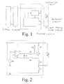
- FIG. 1 shows an overview
- FIG. 2 shows a first embodiment of a bleeder circuit
- FIG. 3 shows waveforms for the first embodiment
- FIG. 4 shows a second embodiment of a bleeder circuit
- FIG. 5 shows a third embodiment of a bleeder circuit
- FIG. 6 shows a fourth embodiment of a bleeder circuit.
- a bleeder circuit 1 for improving a dimming operation of a light emitting diode circuit 2 comprises a detection circuit 11 for detecting a value of an amplitude of a feeding current configured to flow through at least a part of the light emitting diode circuit 2 and comprises an introduction circuit 12 for introducing a bleeder current.
- a value of an amplitude of the bleeder current is defined in response to a detection result from the detection circuit 11 .
- Input terminals of the bleeder circuit 1 are coupled to output terminals of a converter 3 , such as for example a switch mode power supply, without having excluded other kinds of converters.
- Input terminals of the converter 3 are coupled to output terminals of a (phase-cut) dimmer 4 , such as for example a classical triac dimmer, without having excluded other kinds of dimmers.
- Input terminals of the dimmer 4 are coupled to mains.
- a relatively large value of the amplitude of the feeding current will result in a relatively small value of the amplitude of the bleeder current, and a relatively small value of the amplitude of the feeding current will result in a relatively large value of the amplitude of the bleeder current.
- the bleeder circuit 1 will dissipate relatively little power, and vice versa.
- a first embodiment of a bleeder circuit 1 is shown.
- a first input terminal of the bleeder circuit 1 is coupled to a first output terminal of the bleeder circuit 1 .
- a second input terminal of the bleeder circuit 1 is coupled to a second output terminal of the bleeder circuit 1 via a first resistor circuit 31 here in the form of a single resistor, but an embodiment with more than one resistor is not to be excluded.
- the bleeder circuit 1 comprises a first transistor circuit 41 , here in the form of a single transistor, but an embodiment with two or more transistors for example in a Darlington configuration is not to be excluded.
- a first main electrode of the first transistor circuit 41 is coupled via a second resistor circuit 32 to the first resistor circuit 31 and to the second output terminal of the bleeder circuit 1 .
- the second resistor circuit 32 here comprises a single resistor, but an embodiment with more than one resistor is not to be excluded.
- a second main electrode of the first transistor circuit 41 is coupled via a resistor 61 to the first output terminal of the bleeder circuit 1 .
- the resistor 61 reduces a power dissipation in the first transistor circuit 41 , but can be left out without affecting a basic operation of the bleeder circuit 1 .
- a control electrode of the first transistor circuit 41 is coupled via a resistor 62 to the first output terminal of the bleeder circuit 1 and via a resistor 63 to an output of an operational amplifier 51 .
- the resistor 62 allows a control electrode current to be delivered to the control electrode of the first transistor circuit 41 .
- the first main electrode of the first transistor circuit 41 is coupled via a resistor 64 to an inverting input of the operational amplifier 51 .
- a non-inverting input of the operational amplifier 51 is coupled via an external reference source 66 to ground, with the second input terminal of the bleeder circuit 1 being coupled to ground too.
- an operational amplifier with an internal (in-built) reference source may be used.
- the output of the operational amplifier 51 is coupled via a capacitor 65 to the inverting input of the operational amplifier 51 .
- the operational amplifier 51 controls the first transistor circuit 41 to introduce a bleeder current.
- the first resistor circuit 31 and the second resistor circuit 32 and the operational amplifier 51 form part of the detection circuit 11
- the first transistor circuit 41 forms part of the introduction circuit 12 .
- waveforms for the first embodiment shown in the FIG. 2 are shown, vertical axis power (0 Watt to 8 Watt) or current (0 mA to 500 mA), horizontal axis conduction angle of the dimmer (180° to 0°).
- the waveform A shows the power transferred via the converter 3 (or the current flowing through the converter 3 )
- the waveform B shows the power dissipated in the light emitting diode circuit 2 (or the feeding current flowing through the light emitting diode circuit 2 )
- the waveform C shows the power dissipated in the bleeder circuit 1 (or the bleeder current). According to this example, without the bleeder circuit 1 , dimming below 20% is not possible.
- the bleeder circuit 1 With the bleeder circuit 1 , dimming down to 3% has become possible (difference between the waveforms A and B). Clearly, the bleeder circuit 1 enables so called deep dimming, which is a great advantage. The exact gain in deep dimming depends on a transfer function of the converter 3 .
- a second embodiment of a bleeder circuit 1 is shown.
- a first input terminal of the bleeder circuit 1 is coupled to a first output terminal of the bleeder circuit 1 .
- a second input terminal of the bleeder circuit 1 is coupled to a second output terminal of the bleeder circuit 1 via a first resistor circuit 31 here in the form of a single resistor, but an embodiment with more than one resistor is not to be excluded.
- the bleeder circuit 1 comprises a first transistor circuit 41 , here in the form of two transistors in a Darlington configuration, but an embodiment with one or three or more transistors is not to be excluded.
- a first main electrode of the first transistor circuit 41 is coupled via a second resistor circuit 32 to the first resistor circuit 31 and to the second output terminal of the bleeder circuit 1 .
- the second resistor circuit 32 comprises a single resistor, but an embodiment with more than one resistor is not to be excluded.
- a second main electrode of the first transistor circuit 41 is coupled via a resistor 61 to the first output terminal of the bleeder circuit 1 .
- the resistor 61 reduces a power dissipation in the first transistor circuit 41 etc.
- a control electrode of the first transistor circuit 41 is coupled via a resistor 62 to the first output terminal of the bleeder circuit 1 and to a second main electrode of a second transistor circuit 42 , here in the form of a single transistor, but an embodiment with two or more transistors is not to be excluded.
- a first main electrode of the second transistor circuit 42 is coupled to ground, with the second input terminal of the bleeder circuit 1 being coupled to ground too.
- a control electrode of the second transistor circuit 42 is coupled to the first main electrode of the first transistor circuit 41 .
- the second transistor circuit 42 controls the first transistor circuit 41 to introduce a bleeder current.
- the first resistor circuit 31 and the second resistor circuit 32 and the second transistor circuit 42 form part of the detection circuit 11
- the first transistor circuit 41 forms part of the introduction circuit 12 .
- a third embodiment of a bleeder circuit 1 is shown.
- a first input terminal of the bleeder circuit 1 is coupled to a first output terminal of the bleeder circuit 1 .
- a second input terminal of the bleeder circuit 1 is coupled to a second output terminal of the bleeder circuit 1 via a first resistor circuit 31 here in the form of a single resistor etc.
- the bleeder circuit 1 comprises a first transistor circuit 41 , here in the form of a single transistor etc.
- a first main electrode of the first transistor circuit 41 is coupled via a second resistor circuit 32 to the first resistor circuit 31 and to the second output terminal of the bleeder circuit 1 .
- the second resistor circuit 32 comprises a single resistor etc.
- a second main electrode of the first transistor circuit 41 is coupled via a resistor 61 to the first output terminal of the bleeder circuit 1 etc.
- a control electrode of the first transistor circuit 41 is coupled via a resistor 62 to the first output terminal of the bleeder circuit 1 and is coupled to a first input of a current mirror configuration 53 comprising two transistors.
- a first output of the current mirror configuration 53 is coupled to ground via a resistor 74 , with the second input terminal of the bleeder circuit 1 being coupled to ground too.
- a second input of the current mirror configuration 53 is coupled to a first output of a differential amplifier configuration 52 comprising two transistors.
- a second output of the current mirror configuration 53 is coupled to ground via a resistor 73 .
- a second output of the differential amplifier configuration 52 is coupled to ground via a resistor 72 .
- a feeding input of the differential amplifier configuration 52 is coupled via a resistor 71 to an interconnection between a resistor 80 and a capacitor 81 .
- the resistor 80 is further coupled to the first input terminal of the bleeder circuit 1
- the capacitor 81 is further coupled to ground.
- a first control input of the differential amplifier configuration 52 is coupled via a resistor 75 to the interconnection and via a resistor 76 to ground.
- the interconnection is further coupled via a voltage reference element 79 to ground, with a control electrode of the voltage reference element 79 being coupled via a resistor 77 to the interconnection and via a resistor 78 to ground.
- a second control input of the differential amplifier configuration 52 is coupled to the first main electrode of the first transistor circuit 41 .
- the third embodiment of the bleeder circuit 1 shown in the FIG. 5 will perform better because of the differential amplifier configuration 52 and the current mirror configuration 53 .
- the differential amplifier configuration 52 and the current mirror configuration 53 will form part of the detection circuit 11 etc.
- a fourth embodiment of a bleeder circuit 1 is shown.
- a first input terminal of the bleeder circuit 1 is coupled to a first output terminal of the bleeder circuit 1 .
- a second input terminal of the bleeder circuit 1 is coupled to a second output terminal of the bleeder circuit 1 via a first resistor circuit 31 here in the form of a single resistor etc.
- the bleeder circuit 1 comprises a first transistor circuit 41 , here in the form of a single transistor etc.
- a first main electrode of the first transistor circuit 41 is coupled via a second transistor circuit 54 and via a second resistor circuit 32 to the first resistor circuit 31 and to the second output terminal of the bleeder circuit 1 .
- the second resistor circuit 32 comprises a single resistor etc.
- the second transistor circuit 54 here comprises two transistors in a current mirror configuration.
- a second main electrode of the first transistor circuit 41 is coupled via a resistor 61 to the first output terminal of the bleeder circuit 1 etc.
- a control electrode of the first transistor circuit 41 is coupled via a resistor 62 to the first output terminal of the bleeder circuit 1 and to a first input of the current mirror configuration 54 .
- a first output of the current mirror configuration 54 is coupled via a resistor 91 to ground.
- a second input and a second output of the current mirror configuration 54 form said electrodes.
- the current mirror configuration 54 will form part of the detection circuit 11 etc. This current mirror configuration 54 offers good thermal stability.
- the bleeder circuit 1 may further comprise a bypassing circuit 13 for bypassing at least a part of the detection circuit 11 during an inactivity of the bleeder circuit 1 , to reduce a power consumption.
- the bypassing circuit 13 may for example comprise a diode circuit 92 , 93 coupled in parallel to the first resistor circuit 31 of the detection circuit 11 .
- Such a diode circuit 92 , 93 may comprise one diode or two or more for example serially coupled diodes.
- Two elements may be coupled indirectly via a third element or may be coupled directly without a third element being in between.
- a part of one of them may be added to another one of them, and a part of one of them may replace another part in another one of them.
- bleeder circuits 1 comprise detection circuits 11 for detecting values of amplitudes of feeding currents for feeding light emitting diode circuits 2 and comprise introduction circuits 12 for introducing bleeder currents. Values of amplitudes of bleeder currents are defined in response to detection results from the detection circuits 11 .
- the detection circuit 11 may comprise a first resistor circuit 31
- the introduction circuit 12 may comprise a first transistor circuit 41 .
- the detection circuit 11 may further comprise a second resistor circuit 32 for coupling the first transistor circuit 41 to the first resistor circuit 31 and may comprise an operational amplifier 51 or a second transistor circuit 42 for controlling the first transistor circuit 41 .
Landscapes
- Circuit Arrangement For Electric Light Sources In General (AREA)
- Led Devices (AREA)
Applications Claiming Priority (4)
| Application Number | Priority Date | Filing Date | Title |
|---|---|---|---|
| EP13195842.3 | 2013-12-05 | ||
| EP13195842 | 2013-12-05 | ||
| EP13195842 | 2013-12-05 | ||
| PCT/EP2014/076660 WO2015082661A1 (en) | 2013-12-05 | 2014-12-05 | Bleeder for improving dimming of led |
Publications (2)
| Publication Number | Publication Date |
|---|---|
| US20160302272A1 US20160302272A1 (en) | 2016-10-13 |
| US9949325B2 true US9949325B2 (en) | 2018-04-17 |
Family
ID=49683634
Family Applications (1)
| Application Number | Title | Priority Date | Filing Date |
|---|---|---|---|
| US15/038,586 Active US9949325B2 (en) | 2013-12-05 | 2014-12-05 | Bleeder for improving dimming of LED |
Country Status (5)
| Country | Link |
|---|---|
| US (1) | US9949325B2 (enExample) |
| EP (1) | EP3078243B8 (enExample) |
| JP (1) | JP6495911B2 (enExample) |
| CN (1) | CN105794317B (enExample) |
| WO (1) | WO2015082661A1 (enExample) |
Cited By (1)
| Publication number | Priority date | Publication date | Assignee | Title |
|---|---|---|---|---|
| US10652961B2 (en) * | 2018-03-22 | 2020-05-12 | Shaanxi Reactor Microelectronics Co., Ltd | Method for automatically regulating bleeder current and LED silicon-controlled-rectifier dimming circuit |
Families Citing this family (1)
| Publication number | Priority date | Publication date | Assignee | Title |
|---|---|---|---|---|
| CN109392216B (zh) * | 2018-03-22 | 2024-03-08 | 陕西亚成微电子股份有限公司 | 一种泄放电流自调节的方法及led可控硅调光电路 |
Citations (9)
| Publication number | Priority date | Publication date | Assignee | Title |
|---|---|---|---|---|
| US20100090604A1 (en) | 2008-10-09 | 2010-04-15 | Yasuhiro Maruyama | Led drive circuit, led illumination component, led illumination device, and led illumination system |
| WO2010150158A1 (en) | 2009-06-26 | 2010-12-29 | Koninklijke Philips Electronics N.V. | Lighting arrangement comprising magnetic coding means |
| US20110121760A1 (en) | 2009-11-17 | 2011-05-26 | Harrison Daniel J | Led thermal management |
| US20120268040A1 (en) | 2011-04-22 | 2012-10-25 | Scott Riesebosch | Thermal foldback system |
| WO2012168844A2 (en) | 2011-06-10 | 2012-12-13 | Koninklijke Philips Electronics N.V. | Led light source |
| US20120319621A1 (en) * | 2011-06-17 | 2012-12-20 | Sehat Sutardja | Triac dimming systems for solid-state loads |
| WO2013011924A1 (ja) | 2011-07-15 | 2013-01-24 | シチズンホールディングス株式会社 | Led照明装置 |
| US20130187564A1 (en) | 2011-12-16 | 2013-07-25 | Brian Brandt | Transformer voltage detection in dimmable lighting systems |
| US20140239849A1 (en) * | 2013-02-26 | 2014-08-28 | Power Integrations, Inc. | Bleeder circuit having current sense with edge detection |
Family Cites Families (3)
| Publication number | Priority date | Publication date | Assignee | Title |
|---|---|---|---|---|
| ES2427280T3 (es) * | 2009-03-12 | 2013-10-29 | Koninklijke Philips N.V. | Iluminación con LED con comportamiento de temperatura de color de lámpara incandescente |
| JP2011003467A (ja) * | 2009-06-19 | 2011-01-06 | Minebea Co Ltd | 照明装置 |
| EP2797128B1 (en) * | 2011-12-20 | 2017-04-19 | Citizen Watch Co., Ltd. | Led module |
-
2014
- 2014-12-05 WO PCT/EP2014/076660 patent/WO2015082661A1/en not_active Ceased
- 2014-12-05 US US15/038,586 patent/US9949325B2/en active Active
- 2014-12-05 EP EP14815599.7A patent/EP3078243B8/en active Active
- 2014-12-05 JP JP2016536244A patent/JP6495911B2/ja active Active
- 2014-12-05 CN CN201480066454.7A patent/CN105794317B/zh active Active
Patent Citations (9)
| Publication number | Priority date | Publication date | Assignee | Title |
|---|---|---|---|---|
| US20100090604A1 (en) | 2008-10-09 | 2010-04-15 | Yasuhiro Maruyama | Led drive circuit, led illumination component, led illumination device, and led illumination system |
| WO2010150158A1 (en) | 2009-06-26 | 2010-12-29 | Koninklijke Philips Electronics N.V. | Lighting arrangement comprising magnetic coding means |
| US20110121760A1 (en) | 2009-11-17 | 2011-05-26 | Harrison Daniel J | Led thermal management |
| US20120268040A1 (en) | 2011-04-22 | 2012-10-25 | Scott Riesebosch | Thermal foldback system |
| WO2012168844A2 (en) | 2011-06-10 | 2012-12-13 | Koninklijke Philips Electronics N.V. | Led light source |
| US20120319621A1 (en) * | 2011-06-17 | 2012-12-20 | Sehat Sutardja | Triac dimming systems for solid-state loads |
| WO2013011924A1 (ja) | 2011-07-15 | 2013-01-24 | シチズンホールディングス株式会社 | Led照明装置 |
| US20130187564A1 (en) | 2011-12-16 | 2013-07-25 | Brian Brandt | Transformer voltage detection in dimmable lighting systems |
| US20140239849A1 (en) * | 2013-02-26 | 2014-08-28 | Power Integrations, Inc. | Bleeder circuit having current sense with edge detection |
Non-Patent Citations (3)
| Title |
|---|
| Fairchild Semiconductor Corporation, "AN-9745 Design Guide for TRIAC Dimmable LED Driver Using FL7730", www.fairchildsemi.com, Rev. 1.0.2; Oct. 11, 2012, 11 pages total. |
| Watt, "Adaptive Chopping Circuit for Retrofit Dimmable LED Driver", iWatt Inc., Los Gatos CA 95032, APEC 2011, 38 pages total. |
| Watt, "IW3614 AC/DC Digital Power Controller for High Power Factor Dimmable LED Drivers", https://www.iwatt.com, Rev. 0.7, 2013, 18 pages total. |
Cited By (1)
| Publication number | Priority date | Publication date | Assignee | Title |
|---|---|---|---|---|
| US10652961B2 (en) * | 2018-03-22 | 2020-05-12 | Shaanxi Reactor Microelectronics Co., Ltd | Method for automatically regulating bleeder current and LED silicon-controlled-rectifier dimming circuit |
Also Published As
| Publication number | Publication date |
|---|---|
| EP3078243B8 (en) | 2019-04-10 |
| JP2016539477A (ja) | 2016-12-15 |
| EP3078243A1 (en) | 2016-10-12 |
| CN105794317A (zh) | 2016-07-20 |
| WO2015082661A1 (en) | 2015-06-11 |
| CN105794317B (zh) | 2018-11-09 |
| JP6495911B2 (ja) | 2019-04-03 |
| US20160302272A1 (en) | 2016-10-13 |
| EP3078243B1 (en) | 2019-02-27 |
Similar Documents
| Publication | Publication Date | Title |
|---|---|---|
| TWI444093B (zh) | 用以調節負載電流的裝置、方法以及發光系統 | |
| US8723431B2 (en) | Bleeder circuit | |
| US8319449B2 (en) | Controlled voltage source for LED drivers | |
| US8587203B2 (en) | Multiple channel light source power supply with output protection | |
| Li et al. | Novel self-configurable current-mirror techniques for reducing current imbalance in parallel light-emitting diode (LED) strings | |
| CN105247959B (zh) | 用于驱动负载特别是led单元的驱动器设备和驱动方法 | |
| US20180160492A1 (en) | Led current controller | |
| US9974129B1 (en) | Circuit and method for LED current regulation and ripple control | |
| CN103633826B (zh) | 包含功率开关的低电流启动电路 | |
| WO2014126258A1 (ja) | Led駆動回路 | |
| CN110099479A (zh) | Led模块和照明装置 | |
| US9949325B2 (en) | Bleeder for improving dimming of LED | |
| US20210345463A1 (en) | System and method for repurposing 120vac wiring architecture to retrofitable low voltage dc power 2-wire led dimming | |
| EP2640162A1 (en) | Power supply for lighting and luminaire | |
| CN101207953A (zh) | 发光二极管驱动器以及驱动系统 | |
| WO2017012835A1 (en) | Tapped linear driver and driving method | |
| US9629218B1 (en) | Thermal protection for LED bleeder in fault condition | |
| TWI604757B (zh) | Line voltage compensation system for LED constant current control | |
| US9474110B2 (en) | AC direct drive LED power supply capable of handling overvoltage | |
| US10405384B2 (en) | Driving circuit using buck converter capable of generating sufficient voltage to power a LED circuit and associated auxiliary circuitry in a normal mode of operation, and insufficient to power the LED circuit but sufficient to power the associated auxiliary circuitry in an off mode of operation | |
| CN110784100A (zh) | 功率转换装置及功率管理方法 | |
| TWI662859B (zh) | 可隨調光訊號改變響應的回授電路 | |
| JP2019523534A (ja) | シングルチャネルドライバを備えるledランプ | |
| US20170048948A1 (en) | Ac direct drive led power supply capable of handling overvoltage | |
| JP2018018624A (ja) | Led光射出装置 |
Legal Events
| Date | Code | Title | Description |
|---|---|---|---|
| AS | Assignment |
Owner name: KONINKLIJKE PHILIPS N.V., NETHERLANDS Free format text: ASSIGNMENT OF ASSIGNORS INTEREST;ASSIGNORS:BOONEN, PAUL THEODORUS JACOBUS;HONTELE, BERTRAND JOHAN EDWARD;REEL/FRAME:041828/0881 Effective date: 20150202 |
|
| STCF | Information on status: patent grant |
Free format text: PATENTED CASE |
|
| AS | Assignment |
Owner name: PHILIPS LIGHTING HOLDING B.V., NETHERLANDS Free format text: ASSIGNMENT OF ASSIGNORS INTEREST;ASSIGNOR:KONINKLIJKE PHILIPS N.V.;REEL/FRAME:050429/0060 Effective date: 20160201 |
|
| AS | Assignment |
Owner name: SIGNIFY HOLDING B.V., NETHERLANDS Free format text: CHANGE OF NAME;ASSIGNOR:PHILIPS LIGHTING HOLDING B.V.;REEL/FRAME:050837/0576 Effective date: 20190201 |
|
| MAFP | Maintenance fee payment |
Free format text: PAYMENT OF MAINTENANCE FEE, 4TH YEAR, LARGE ENTITY (ORIGINAL EVENT CODE: M1551); ENTITY STATUS OF PATENT OWNER: LARGE ENTITY Year of fee payment: 4 |
|
| MAFP | Maintenance fee payment |
Free format text: PAYMENT OF MAINTENANCE FEE, 8TH YEAR, LARGE ENTITY (ORIGINAL EVENT CODE: M1552); ENTITY STATUS OF PATENT OWNER: LARGE ENTITY Year of fee payment: 8 |