US9905533B2 - Method for producing a semi-conductor arrangement and corresponding semi-conductor arrangement - Google Patents
Method for producing a semi-conductor arrangement and corresponding semi-conductor arrangement Download PDFInfo
- Publication number
- US9905533B2 US9905533B2 US15/514,304 US201515514304A US9905533B2 US 9905533 B2 US9905533 B2 US 9905533B2 US 201515514304 A US201515514304 A US 201515514304A US 9905533 B2 US9905533 B2 US 9905533B2
- Authority
- US
- United States
- Prior art keywords
- base element
- semiconductor
- layer
- sintered layer
- region
- Prior art date
- Legal status (The legal status is an assumption and is not a legal conclusion. Google has not performed a legal analysis and makes no representation as to the accuracy of the status listed.)
- Active
Links
Images


Classifications
-
- H—ELECTRICITY
- H01—ELECTRIC ELEMENTS
- H01L—SEMICONDUCTOR DEVICES NOT COVERED BY CLASS H10
- H01L24/00—Arrangements for connecting or disconnecting semiconductor or solid-state bodies; Methods or apparatus related thereto
- H01L24/80—Methods for connecting semiconductor or other solid state bodies using means for bonding being attached to, or being formed on, the surface to be connected
- H01L24/83—Methods for connecting semiconductor or other solid state bodies using means for bonding being attached to, or being formed on, the surface to be connected using a layer connector
-
- H—ELECTRICITY
- H01—ELECTRIC ELEMENTS
- H01L—SEMICONDUCTOR DEVICES NOT COVERED BY CLASS H10
- H01L21/00—Processes or apparatus adapted for the manufacture or treatment of semiconductor or solid state devices or of parts thereof
- H01L21/02—Manufacture or treatment of semiconductor devices or of parts thereof
- H01L21/04—Manufacture or treatment of semiconductor devices or of parts thereof the devices having at least one potential-jump barrier or surface barrier, e.g. PN junction, depletion layer or carrier concentration layer
- H01L21/48—Manufacture or treatment of parts, e.g. containers, prior to assembly of the devices, using processes not provided for in a single one of the subgroups H01L21/06 - H01L21/326
- H01L21/4814—Conductive parts
- H01L21/4871—Bases, plates or heatsinks
-
- H—ELECTRICITY
- H01—ELECTRIC ELEMENTS
- H01L—SEMICONDUCTOR DEVICES NOT COVERED BY CLASS H10
- H01L23/00—Details of semiconductor or other solid state devices
- H01L23/48—Arrangements for conducting electric current to or from the solid state body in operation, e.g. leads, terminal arrangements ; Selection of materials therefor
- H01L23/488—Arrangements for conducting electric current to or from the solid state body in operation, e.g. leads, terminal arrangements ; Selection of materials therefor consisting of soldered or bonded constructions
- H01L23/492—Bases or plates or solder therefor
-
- H—ELECTRICITY
- H01—ELECTRIC ELEMENTS
- H01L—SEMICONDUCTOR DEVICES NOT COVERED BY CLASS H10
- H01L24/00—Arrangements for connecting or disconnecting semiconductor or solid-state bodies; Methods or apparatus related thereto
- H01L24/01—Means for bonding being attached to, or being formed on, the surface to be connected, e.g. chip-to-package, die-attach, "first-level" interconnects; Manufacturing methods related thereto
- H01L24/26—Layer connectors, e.g. plate connectors, solder or adhesive layers; Manufacturing methods related thereto
- H01L24/31—Structure, shape, material or disposition of the layer connectors after the connecting process
- H01L24/32—Structure, shape, material or disposition of the layer connectors after the connecting process of an individual layer connector
-
- H—ELECTRICITY
- H01—ELECTRIC ELEMENTS
- H01L—SEMICONDUCTOR DEVICES NOT COVERED BY CLASS H10
- H01L2224/00—Indexing scheme for arrangements for connecting or disconnecting semiconductor or solid-state bodies and methods related thereto as covered by H01L24/00
- H01L2224/01—Means for bonding being attached to, or being formed on, the surface to be connected, e.g. chip-to-package, die-attach, "first-level" interconnects; Manufacturing methods related thereto
- H01L2224/02—Bonding areas; Manufacturing methods related thereto
- H01L2224/04—Structure, shape, material or disposition of the bonding areas prior to the connecting process
- H01L2224/04026—Bonding areas specifically adapted for layer connectors
-
- H—ELECTRICITY
- H01—ELECTRIC ELEMENTS
- H01L—SEMICONDUCTOR DEVICES NOT COVERED BY CLASS H10
- H01L2224/00—Indexing scheme for arrangements for connecting or disconnecting semiconductor or solid-state bodies and methods related thereto as covered by H01L24/00
- H01L2224/01—Means for bonding being attached to, or being formed on, the surface to be connected, e.g. chip-to-package, die-attach, "first-level" interconnects; Manufacturing methods related thereto
- H01L2224/02—Bonding areas; Manufacturing methods related thereto
- H01L2224/04—Structure, shape, material or disposition of the bonding areas prior to the connecting process
- H01L2224/05—Structure, shape, material or disposition of the bonding areas prior to the connecting process of an individual bonding area
- H01L2224/0554—External layer
- H01L2224/0556—Disposition
- H01L2224/05568—Disposition the whole external layer protruding from the surface
-
- H—ELECTRICITY
- H01—ELECTRIC ELEMENTS
- H01L—SEMICONDUCTOR DEVICES NOT COVERED BY CLASS H10
- H01L2224/00—Indexing scheme for arrangements for connecting or disconnecting semiconductor or solid-state bodies and methods related thereto as covered by H01L24/00
- H01L2224/01—Means for bonding being attached to, or being formed on, the surface to be connected, e.g. chip-to-package, die-attach, "first-level" interconnects; Manufacturing methods related thereto
- H01L2224/02—Bonding areas; Manufacturing methods related thereto
- H01L2224/04—Structure, shape, material or disposition of the bonding areas prior to the connecting process
- H01L2224/05—Structure, shape, material or disposition of the bonding areas prior to the connecting process of an individual bonding area
- H01L2224/0554—External layer
- H01L2224/05599—Material
- H01L2224/056—Material with a principal constituent of the material being a metal or a metalloid, e.g. boron [B], silicon [Si], germanium [Ge], arsenic [As], antimony [Sb], tellurium [Te] and polonium [Po], and alloys thereof
- H01L2224/05638—Material with a principal constituent of the material being a metal or a metalloid, e.g. boron [B], silicon [Si], germanium [Ge], arsenic [As], antimony [Sb], tellurium [Te] and polonium [Po], and alloys thereof the principal constituent melting at a temperature of greater than or equal to 950°C and less than 1550°C
- H01L2224/05647—Copper [Cu] as principal constituent
-
- H—ELECTRICITY
- H01—ELECTRIC ELEMENTS
- H01L—SEMICONDUCTOR DEVICES NOT COVERED BY CLASS H10
- H01L2224/00—Indexing scheme for arrangements for connecting or disconnecting semiconductor or solid-state bodies and methods related thereto as covered by H01L24/00
- H01L2224/01—Means for bonding being attached to, or being formed on, the surface to be connected, e.g. chip-to-package, die-attach, "first-level" interconnects; Manufacturing methods related thereto
- H01L2224/26—Layer connectors, e.g. plate connectors, solder or adhesive layers; Manufacturing methods related thereto
- H01L2224/28—Structure, shape, material or disposition of the layer connectors prior to the connecting process
- H01L2224/29—Structure, shape, material or disposition of the layer connectors prior to the connecting process of an individual layer connector
- H01L2224/29001—Core members of the layer connector
- H01L2224/29005—Structure
- H01L2224/29007—Layer connector smaller than the underlying bonding area
-
- H—ELECTRICITY
- H01—ELECTRIC ELEMENTS
- H01L—SEMICONDUCTOR DEVICES NOT COVERED BY CLASS H10
- H01L2224/00—Indexing scheme for arrangements for connecting or disconnecting semiconductor or solid-state bodies and methods related thereto as covered by H01L24/00
- H01L2224/01—Means for bonding being attached to, or being formed on, the surface to be connected, e.g. chip-to-package, die-attach, "first-level" interconnects; Manufacturing methods related thereto
- H01L2224/26—Layer connectors, e.g. plate connectors, solder or adhesive layers; Manufacturing methods related thereto
- H01L2224/28—Structure, shape, material or disposition of the layer connectors prior to the connecting process
- H01L2224/29—Structure, shape, material or disposition of the layer connectors prior to the connecting process of an individual layer connector
- H01L2224/29001—Core members of the layer connector
- H01L2224/2902—Disposition
- H01L2224/29034—Disposition the layer connector covering only portions of the surface to be connected
- H01L2224/29036—Disposition the layer connector covering only portions of the surface to be connected covering only the central area of the surface to be connected
-
- H—ELECTRICITY
- H01—ELECTRIC ELEMENTS
- H01L—SEMICONDUCTOR DEVICES NOT COVERED BY CLASS H10
- H01L2224/00—Indexing scheme for arrangements for connecting or disconnecting semiconductor or solid-state bodies and methods related thereto as covered by H01L24/00
- H01L2224/01—Means for bonding being attached to, or being formed on, the surface to be connected, e.g. chip-to-package, die-attach, "first-level" interconnects; Manufacturing methods related thereto
- H01L2224/26—Layer connectors, e.g. plate connectors, solder or adhesive layers; Manufacturing methods related thereto
- H01L2224/28—Structure, shape, material or disposition of the layer connectors prior to the connecting process
- H01L2224/29—Structure, shape, material or disposition of the layer connectors prior to the connecting process of an individual layer connector
- H01L2224/29001—Core members of the layer connector
- H01L2224/29099—Material
- H01L2224/291—Material with a principal constituent of the material being a metal or a metalloid, e.g. boron [B], silicon [Si], germanium [Ge], arsenic [As], antimony [Sb], tellurium [Te] and polonium [Po], and alloys thereof
-
- H—ELECTRICITY
- H01—ELECTRIC ELEMENTS
- H01L—SEMICONDUCTOR DEVICES NOT COVERED BY CLASS H10
- H01L2224/00—Indexing scheme for arrangements for connecting or disconnecting semiconductor or solid-state bodies and methods related thereto as covered by H01L24/00
- H01L2224/01—Means for bonding being attached to, or being formed on, the surface to be connected, e.g. chip-to-package, die-attach, "first-level" interconnects; Manufacturing methods related thereto
- H01L2224/26—Layer connectors, e.g. plate connectors, solder or adhesive layers; Manufacturing methods related thereto
- H01L2224/31—Structure, shape, material or disposition of the layer connectors after the connecting process
- H01L2224/32—Structure, shape, material or disposition of the layer connectors after the connecting process of an individual layer connector
- H01L2224/3201—Structure
- H01L2224/32012—Structure relative to the bonding area, e.g. bond pad
- H01L2224/32013—Structure relative to the bonding area, e.g. bond pad the layer connector being larger than the bonding area, e.g. bond pad
-
- H—ELECTRICITY
- H01—ELECTRIC ELEMENTS
- H01L—SEMICONDUCTOR DEVICES NOT COVERED BY CLASS H10
- H01L2224/00—Indexing scheme for arrangements for connecting or disconnecting semiconductor or solid-state bodies and methods related thereto as covered by H01L24/00
- H01L2224/01—Means for bonding being attached to, or being formed on, the surface to be connected, e.g. chip-to-package, die-attach, "first-level" interconnects; Manufacturing methods related thereto
- H01L2224/26—Layer connectors, e.g. plate connectors, solder or adhesive layers; Manufacturing methods related thereto
- H01L2224/31—Structure, shape, material or disposition of the layer connectors after the connecting process
- H01L2224/32—Structure, shape, material or disposition of the layer connectors after the connecting process of an individual layer connector
- H01L2224/321—Disposition
- H01L2224/32151—Disposition the layer connector connecting between a semiconductor or solid-state body and an item not being a semiconductor or solid-state body, e.g. chip-to-substrate, chip-to-passive
- H01L2224/32221—Disposition the layer connector connecting between a semiconductor or solid-state body and an item not being a semiconductor or solid-state body, e.g. chip-to-substrate, chip-to-passive the body and the item being stacked
- H01L2224/32225—Disposition the layer connector connecting between a semiconductor or solid-state body and an item not being a semiconductor or solid-state body, e.g. chip-to-substrate, chip-to-passive the body and the item being stacked the item being non-metallic, e.g. insulating substrate with or without metallisation
- H01L2224/32227—Disposition the layer connector connecting between a semiconductor or solid-state body and an item not being a semiconductor or solid-state body, e.g. chip-to-substrate, chip-to-passive the body and the item being stacked the item being non-metallic, e.g. insulating substrate with or without metallisation the layer connector connecting to a bond pad of the item
-
- H—ELECTRICITY
- H01—ELECTRIC ELEMENTS
- H01L—SEMICONDUCTOR DEVICES NOT COVERED BY CLASS H10
- H01L2224/00—Indexing scheme for arrangements for connecting or disconnecting semiconductor or solid-state bodies and methods related thereto as covered by H01L24/00
- H01L2224/01—Means for bonding being attached to, or being formed on, the surface to be connected, e.g. chip-to-package, die-attach, "first-level" interconnects; Manufacturing methods related thereto
- H01L2224/26—Layer connectors, e.g. plate connectors, solder or adhesive layers; Manufacturing methods related thereto
- H01L2224/31—Structure, shape, material or disposition of the layer connectors after the connecting process
- H01L2224/32—Structure, shape, material or disposition of the layer connectors after the connecting process of an individual layer connector
- H01L2224/321—Disposition
- H01L2224/32151—Disposition the layer connector connecting between a semiconductor or solid-state body and an item not being a semiconductor or solid-state body, e.g. chip-to-substrate, chip-to-passive
- H01L2224/32221—Disposition the layer connector connecting between a semiconductor or solid-state body and an item not being a semiconductor or solid-state body, e.g. chip-to-substrate, chip-to-passive the body and the item being stacked
- H01L2224/32245—Disposition the layer connector connecting between a semiconductor or solid-state body and an item not being a semiconductor or solid-state body, e.g. chip-to-substrate, chip-to-passive the body and the item being stacked the item being metallic
-
- H—ELECTRICITY
- H01—ELECTRIC ELEMENTS
- H01L—SEMICONDUCTOR DEVICES NOT COVERED BY CLASS H10
- H01L2224/00—Indexing scheme for arrangements for connecting or disconnecting semiconductor or solid-state bodies and methods related thereto as covered by H01L24/00
- H01L2224/80—Methods for connecting semiconductor or other solid state bodies using means for bonding being attached to, or being formed on, the surface to be connected
- H01L2224/83—Methods for connecting semiconductor or other solid state bodies using means for bonding being attached to, or being formed on, the surface to be connected using a layer connector
- H01L2224/8338—Bonding interfaces outside the semiconductor or solid-state body
- H01L2224/83385—Shape, e.g. interlocking features
-
- H—ELECTRICITY
- H01—ELECTRIC ELEMENTS
- H01L—SEMICONDUCTOR DEVICES NOT COVERED BY CLASS H10
- H01L2224/00—Indexing scheme for arrangements for connecting or disconnecting semiconductor or solid-state bodies and methods related thereto as covered by H01L24/00
- H01L2224/80—Methods for connecting semiconductor or other solid state bodies using means for bonding being attached to, or being formed on, the surface to be connected
- H01L2224/83—Methods for connecting semiconductor or other solid state bodies using means for bonding being attached to, or being formed on, the surface to be connected using a layer connector
- H01L2224/838—Bonding techniques
- H01L2224/8384—Sintering
-
- H—ELECTRICITY
- H01—ELECTRIC ELEMENTS
- H01L—SEMICONDUCTOR DEVICES NOT COVERED BY CLASS H10
- H01L2924/00—Indexing scheme for arrangements or methods for connecting or disconnecting semiconductor or solid-state bodies as covered by H01L24/00
- H01L2924/10—Details of semiconductor or other solid state devices to be connected
- H01L2924/11—Device type
- H01L2924/12—Passive devices, e.g. 2 terminal devices
- H01L2924/1203—Rectifying Diode
-
- H—ELECTRICITY
- H01—ELECTRIC ELEMENTS
- H01L—SEMICONDUCTOR DEVICES NOT COVERED BY CLASS H10
- H01L2924/00—Indexing scheme for arrangements or methods for connecting or disconnecting semiconductor or solid-state bodies as covered by H01L24/00
- H01L2924/10—Details of semiconductor or other solid state devices to be connected
- H01L2924/11—Device type
- H01L2924/13—Discrete devices, e.g. 3 terminal devices
- H01L2924/1304—Transistor
- H01L2924/1305—Bipolar Junction Transistor [BJT]
- H01L2924/13055—Insulated gate bipolar transistor [IGBT]
-
- H—ELECTRICITY
- H01—ELECTRIC ELEMENTS
- H01L—SEMICONDUCTOR DEVICES NOT COVERED BY CLASS H10
- H01L2924/00—Indexing scheme for arrangements or methods for connecting or disconnecting semiconductor or solid-state bodies as covered by H01L24/00
- H01L2924/10—Details of semiconductor or other solid state devices to be connected
- H01L2924/11—Device type
- H01L2924/13—Discrete devices, e.g. 3 terminal devices
- H01L2924/1304—Transistor
- H01L2924/1306—Field-effect transistor [FET]
- H01L2924/13091—Metal-Oxide-Semiconductor Field-Effect Transistor [MOSFET]
-
- H—ELECTRICITY
- H01—ELECTRIC ELEMENTS
- H01L—SEMICONDUCTOR DEVICES NOT COVERED BY CLASS H10
- H01L2924/00—Indexing scheme for arrangements or methods for connecting or disconnecting semiconductor or solid-state bodies as covered by H01L24/00
- H01L2924/30—Technical effects
- H01L2924/35—Mechanical effects
- H01L2924/351—Thermal stress
- H01L2924/3512—Cracking
Definitions
- the invention relates a method for producing a semiconductor arrangement with at least one base element and a semiconductor, wherein the semiconductor is fastened on the base element by means of a center layer.
- the invention also relates to a semiconductor arrangement.
- the semiconductor arrangement is made at least of the base element and the semiconductor.
- the base element is for example a base plate or a bottom plate.
- the base element can serve as a cooling body via which heat generated at the semiconductor can be dissipated to an environment of the semiconductor arrangement.
- the semiconductor is preferably fastened solder-free on the base element, i.e., in the absence of solder.
- the at least one center layer is provided, which is situated between the semiconductor and the base element.
- the center layer does not necessarily directly contact the base element and/or the semiconductor, i.e., for example the center layer does not necessarily have to be arranged between the base element and the semiconductor. Rather it may be provided that at least one intermediate layer is present between the base element and the semiconductor.
- this intermediate layer is fastened on the base element by means of the sintered layer, in particular directly so that as a result the sintered layer contacts the intermediate layer on one side and the base element on the other side.
- a further sintered layer can serve for fastening the semiconductor on the intermediate layer, so that for example the further sintered layer contacts the semiconductor as well as the intermediate layer.
- a region of the base element, which directly contacts the sintered layer is at least partially perforated.
- the sintered layer is thus in contact with this region.
- This region is at least partially perforated, i.e., it is provided with at least one recess.
- the recess can generally be configured arbitrarily.
- the recess can for example have the form of a through-opening or a blind recess, wherein the former traverses the base element while the latter has a closed bottom.
- the blind recess is preferably only open in the direction of the sintered layer, i.e., it traverses a surface of the base element in that region with which the sintered layer is in direct contact.
- the stiffness of the base element can be adjusted in a targeted manner and thus its expansion behavior can be influenced. In this way the stress on the sintered layer due to thermal tensions is significantly reduced thereby improving the service life of the semiconductor arrangement.
- the perforation is performed prior to the fastening of the semiconductor on the base element.
- the base element thus has the perforation or the at least one recess already prior to the process of the sintering and/or the application of the green compact from which the sintered layer is made. This generally constitutes the simplest and most cost effective configuration.
- the perforation also improves the fastening by means of the sintered layer because the sintered layer or the green compact for the sintered layer can be introduced at least in regions into the perforation or the at least one recess when being applied onto the base element.
- the sintered layer or the green compact can also be configured planar on its side that faces the base element or can rest planar against the base element.
- the perforating includes generating at least one recess, in particular a plurality of recesses including the region of the base element.
- the perforation includes the at least one recess.
- a plurality of recesses is realized, wherein the recesses are in particular spaced apart from each other in the region of the base element.
- the recesses can be identical or different from each other.
- the recess are circular in cross section.
- all recesses can be configured as oblong holes, i.e., they can for example have an oval or stadium-like cross section. The latter means that when viewed in cross section the recess is delimited by two parallel lines, which are connected on both sides by a curved line, for example a semicircle.
- At least a subset of the recesses can be configured as a through-opening.
- all recesses are configured as through-openings.
- a further subset can be configured as blind recess.
- all recesses are configured as blind recesses.
- the recesses can have the same distance to each other. However, they can also be arranged unevenly distributed over the region.
- the at least one recess is configured as a through-opening with a closed border.
- the configuration of the recess as through-opening was mentioned above. This means that the recess completely traverses the base element.
- the recess is to be present in the base element so that when viewed in cross section the recess has a closed border, i.e., when viewed in cross section it has a closed boundary.
- the recess is in particular not to traverse a border of the base element.
- the base element has a planar surface, which is traversed by the at least one recess and which the sintered layer contacts after fastening of the semiconductor.
- the region of the base element, which the sintered layer contacts, is thus planar or is configured as a planar surface.
- the base element is configured so that a region of the base element, which is angled with respect to the surface, adjoins the planar surface.
- the base element is insofar not configured completely planar but besides the planar surface, which the sintered layer contacts, has the angled region.
- the angled region is also planar and encloses with the planar surface an angle of at least 10°, at least 20°, at least 30°, at least 40°, at least 45°, at least 50°, at least 60°, at least 70°, at least 80° or exactly 90°.
- the angle is in any case at most 90°.
- Such an angled region respectively directly adjoins the planar surface on both sides of the planar surface.
- a further planar surface adjoins, which can be parallel to the planar surface.
- regions, which in normal direction of the planar surface are spaced farther apart from the sintered layer than the planar surface, adjoin the region of the base element, which i sin direct contact with the sintered layer.
- these further regions are not perforated but are constructed solid. These regions can in particular be configured as cooling ribs via which heat generated at the semiconductor is dissipated to the environment of the semiconductor arrangement.
- a contact layer is applied on the semiconductor.
- the semiconductor is thus not directly fastened on the base element but rather indirectly via the contact layer by means of the sintered layer.
- Fastening of the contact layer on the base element is in particular performed by means of the sintered layer, so that the sintered layer is in direct contact with the base element as well as with the contact layer.
- a DCB-layer or an IMS-layer is used as contact layer.
- the contact layer can thus also be referred to as DCB-substrate and the IMS layer as IMS-substrate.
- DCB-substrate means a multilayered construction made of two outer copper layers and an intermediate layer.
- the intermediate layer is for example made of ceramic or aluminum, in particular of AL 2 O 3 , Si 3 N 4 or AlN.
- IMS-layer IMS: Insulated Metal Substrate
- an IGBT, a diode or a MOSFET is used as semiconductor.
- the semiconductor can generally be configured arbitrarily.
- the problem of the thermal tension is particularly pronounced.
- the invention also relates to a semiconductor arrangement, in particular produced according to the description above with at least one base element and a semiconductor, wherein the semiconductor is fastened on the base element by means of the sintered layer.
- a region of the base element, which directly contacts the sintered layer is perforated at least in regions.
- FIG. 1 a cross sectional view through a region of a semiconductor arrangement, which has a base element and a semiconductor fastened on the base element by means of a sintered layer, and
- FIG. 2 a detail view of the base element.
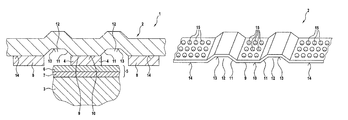
- FIG. 1 shows a cross sectional view of a semiconductor arrangement 1 with a base element 2 and a semiconductor 3 , of which here only a section is shown.
- the semiconductor 3 is fastened on the base element 2 by means of a sintered layer 4 .
- the sintered layer 4 engages on one side directly on the base element 2 and on the other side directly on the contact layer 5 , which is for example configured as a DCB-layer and thus has a copper layer 6 and a substrate layer 7 .
- the substrate layer 7 is preferably made of Al 2 O 3 .
- the sintered layer 4 at least one further sintered layer, in the here shown exemplary embodiment two further sintered layers 8 , can be provided.
- the sintered layer 8 directly contacts the base element 2 in a region 9 of the base element, wherein the base element 2 in this region has a planar surface 10 .
- an angled region 11 of the base element 2 adjoins this planar surface 10 .
- Preferably such a region 11 is present on each side of the surface 10 .
- the regions 11 indentations 12 are formed in the base element 2 , with the base 13 of the indentations preferably being planar and extending parallel to the planar surface 10 .
- the base 13 of the indentations preferably being planar and extending parallel to the planar surface 10 .
- a further planar surface 14 can be present on the side of the indentation 12 that faces away from the surface 10 or the substrate layer 7 .
- the surface 14 can be parallel to the surface 10 and/or be situated in the same imagined plane as the surface 10 .
- FIG. 2 shows a detail view of the base element 2 .
- the base element 2 in the region 9 which is in direct contact with the sintered layer 4 (here not shown), is perforated at least in regions, i.e., it has at least one recess 15 , in particular a plurality of recesses 15 of which here only one is exemplarily shown.
- the surface 14 on which a sintered layer 8 can also be arranged can also be provided with at least one such recess 15 .
- the recesses 15 are formed as through-openings and in cross section have a closed border and are circular.
- the recesses 15 can also be configured as blind recesses and/or can have any other cross sectional configuration.
- the stiffness of the base element 2 can be reduced in regions thus facilitating elastic deformation of the base element 2 in the case of thermal tensions between the sintered layer 4 and the base element 2 . In this way damage to the sintered layer 4 and/or the semiconductor 3 due to these thermal tensions is prevented or at least reduced.
Abstract
A method for producing a semiconductor arrangement, said method includes fastening a semiconductor on a base element by means of a sintered layer, wherein a side of the sintered layer which faces the base element is configured planar; and perforating a region of the base element, which directly contacts the sinter, wherein the perforating includes generating a plurality of through-openings having a closed border in the region of the base element for adjusting a stiffness of at least a portion of the base element in a targeted manner
Description
This application is the U.S. National Stage of International Application No. PCT/EP2015/001393, filed Jul. 8, 2015, which designated the United States and has been published as International Publication No, WO 2016/045758 and which claims the priority of German Patent Application, Serial No. 10 2014 014 473.9, filed Sep. 27, 2014, pursuant to 35 U.S.C. 119(a)-(d),
The invention relates a method for producing a semiconductor arrangement with at least one base element and a semiconductor, wherein the semiconductor is fastened on the base element by means of a center layer. The invention also relates to a semiconductor arrangement.
The semiconductor arrangement is made at least of the base element and the semiconductor. The base element is for example a base plate or a bottom plate. The base element can serve as a cooling body via which heat generated at the semiconductor can be dissipated to an environment of the semiconductor arrangement. The semiconductor is preferably fastened solder-free on the base element, i.e., in the absence of solder. For this purpose the at least one center layer is provided, which is situated between the semiconductor and the base element.
The center layer does not necessarily directly contact the base element and/or the semiconductor, i.e., for example the center layer does not necessarily have to be arranged between the base element and the semiconductor. Rather it may be provided that at least one intermediate layer is present between the base element and the semiconductor.
It can be provided that this intermediate layer is fastened on the base element by means of the sintered layer, in particular directly so that as a result the sintered layer contacts the intermediate layer on one side and the base element on the other side. A further sintered layer can serve for fastening the semiconductor on the intermediate layer, so that for example the further sintered layer contacts the semiconductor as well as the intermediate layer.
During operation of such a semiconductor arrangement significant temperature stress may occur, which generates thermal tensions, which in particular act on the semiconductor and/or the sintered layer. This may lead to accelerated aging of the semiconductor arrangement, in particular due to cracks that may form in the center layer.
It is therefore an object of the invention to propose a method for producing a semiconductor arrangement, which has advantages compared to the state of the art and in particular avoids or at least reduces the mentioned disadvantage of crack formation due to thermal tensions.
This is achieved according to the invention with a method with the features of the independent claim. Hereby it is provided that a region of the base element, which directly contacts the sintered layer, is at least partially perforated. In at least one region of the base element the sintered layer is thus in contact with this region. This region is at least partially perforated, i.e., it is provided with at least one recess.
The recess can generally be configured arbitrarily. The recess can for example have the form of a through-opening or a blind recess, wherein the former traverses the base element while the latter has a closed bottom. The blind recess is preferably only open in the direction of the sintered layer, i.e., it traverses a surface of the base element in that region with which the sintered layer is in direct contact.
By means of the perforation the stiffness of the base element can be adjusted in a targeted manner and thus its expansion behavior can be influenced. In this way the stress on the sintered layer due to thermal tensions is significantly reduced thereby improving the service life of the semiconductor arrangement.
In a further embodiment of the invention it is provided that the perforation is performed prior to the fastening of the semiconductor on the base element. The base element thus has the perforation or the at least one recess already prior to the process of the sintering and/or the application of the green compact from which the sintered layer is made. This generally constitutes the simplest and most cost effective configuration.
In addition the perforation also improves the fastening by means of the sintered layer because the sintered layer or the green compact for the sintered layer can be introduced at least in regions into the perforation or the at least one recess when being applied onto the base element. However, this is only optional. Of course the sintered layer or the green compact can also be configured planar on its side that faces the base element or can rest planar against the base element.
In a further preferred embodiment of the invention it is provided that the perforating includes generating at least one recess, in particular a plurality of recesses including the region of the base element. As mentioned above the perforation includes the at least one recess. However, particularly preferably a plurality of recesses is realized, wherein the recesses are in particular spaced apart from each other in the region of the base element. Hereby the recesses can be identical or different from each other.
For example at least a subset of the recess, in particular all recesses, are circular in cross section. However a further subset of the recesses or, as an alternative, all recesses can be configured as oblong holes, i.e., they can for example have an oval or stadium-like cross section. The latter means that when viewed in cross section the recess is delimited by two parallel lines, which are connected on both sides by a curved line, for example a semicircle.
In addition or as an alternative at least a subset of the recesses can be configured as a through-opening. Preferably all recesses are configured as through-openings. However in addition or as alternative a further subset can be configured as blind recess. For example all recesses are configured as blind recesses. In an embodiment the recesses can have the same distance to each other. However, they can also be arranged unevenly distributed over the region.
In a further embodiment of the invention it is provided that the at least one recess is configured as a through-opening with a closed border. The configuration of the recess as through-opening was mentioned above. This means that the recess completely traverses the base element. However, the recess is to be present in the base element so that when viewed in cross section the recess has a closed border, i.e., when viewed in cross section it has a closed boundary. The recess is in particular not to traverse a border of the base element.
In a further preferred embodiment of the invention it is provided that the base element has a planar surface, which is traversed by the at least one recess and which the sintered layer contacts after fastening of the semiconductor. The region of the base element, which the sintered layer contacts, is thus planar or is configured as a planar surface.
An embodiment of the invention provides that the base element is configured so that a region of the base element, which is angled with respect to the surface, adjoins the planar surface. The base element is insofar not configured completely planar but besides the planar surface, which the sintered layer contacts, has the angled region. For example the angled region is also planar and encloses with the planar surface an angle of at least 10°, at least 20°, at least 30°, at least 40°, at least 45°, at least 50°, at least 60°, at least 70°, at least 80° or exactly 90°. The angle is in any case at most 90°.
It can be provided that such an angled region respectively directly adjoins the planar surface on both sides of the planar surface. In addition or as an alternative it can be provided that on a side of the region, which faces away from the planar surface, a further planar surface adjoins, which can be parallel to the planar surface. In other words regions, which in normal direction of the planar surface are spaced farther apart from the sintered layer than the planar surface, adjoin the region of the base element, which i sin direct contact with the sintered layer. Preferably these further regions are not perforated but are constructed solid. These regions can in particular be configured as cooling ribs via which heat generated at the semiconductor is dissipated to the environment of the semiconductor arrangement.
In an embodiment of the invention it is provided that prior to the fastening a contact layer is applied on the semiconductor. The semiconductor is thus not directly fastened on the base element but rather indirectly via the contact layer by means of the sintered layer. Fastening of the contact layer on the base element is in particular performed by means of the sintered layer, so that the sintered layer is in direct contact with the base element as well as with the contact layer.
In an advantageous embodiment of the invention it is provided that a DCB-layer or an IMS-layer is used as contact layer. The contact layer can thus also be referred to as DCB-substrate and the IMS layer as IMS-substrate. The term DCB-substrate means a multilayered construction made of two outer copper layers and an intermediate layer. The intermediate layer is for example made of ceramic or aluminum, in particular of AL2O3, Si3N4 or AlN. The term IMS-layer (IMS: Insulated Metal Substrate) means for example an aluminum core conductor plate.
Finally it can be provided that an IGBT, a diode or a MOSFET is used as semiconductor. However, the semiconductor can generally be configured arbitrarily. However, in the mentioned embodiments the problem of the thermal tension is particularly pronounced.
The invention also relates to a semiconductor arrangement, in particular produced according to the description above with at least one base element and a semiconductor, wherein the semiconductor is fastened on the base element by means of the sintered layer. Hereby it is provided that a region of the base element, which directly contacts the sintered layer, is perforated at least in regions. The advantages of such a configuration of the semiconductor arrangement or the method were described above. The semiconductor arrangement as well as the method can be further refined according to the description above so that reference is made thereto.
In the following the invention is explained in more detail by way of the exemplary embodiments shown in the drawing without limiting the invention. Hereby it is shown in
Besides the sintered layer 4 at least one further sintered layer, in the here shown exemplary embodiment two further sintered layers 8, can be provided. The sintered layer 8 directly contacts the base element 2 in a region 9 of the base element, wherein the base element 2 in this region has a planar surface 10. In the here shown view of the semiconductor arrangement 1 it can be seen that an angled region 11 of the base element 2 adjoins this planar surface 10. Preferably such a region 11 is present on each side of the surface 10.
As a result of the regions 11 indentations 12 are formed in the base element 2, with the base 13 of the indentations preferably being planar and extending parallel to the planar surface 10. On the side of the indentation 12 that faces away from the surface 10 or the substrate layer 7 a further planar surface 14 can be present. The surface 14 can be parallel to the surface 10 and/or be situated in the same imagined plane as the surface 10.
By means of the perforation of the region 9 and preferably also of the surface 14 the stiffness of the base element 2 can be reduced in regions thus facilitating elastic deformation of the base element 2 in the case of thermal tensions between the sintered layer 4 and the base element 2. In this way damage to the sintered layer 4 and/or the semiconductor 3 due to these thermal tensions is prevented or at least reduced.
Claims (8)
1. A method for producing a semiconductor arrangement, said method comprising:
fastening a semiconductor on a base element by means of a sintered layer, wherein a side of the sintered layer which faces the base element is configured planar; and
perforating a region of the base element, which directly contacts the sintered layer, said perforating comprising generating a plurality of recesses configured as through-openings having a closed border in the region of the base element for adjusting a stiffness of at least a portion of the base element in a targeted manner.
2. The method of claim 1 , wherein the perforating is performed prior to the fastening of the semiconductor on the base element.
3. The method of claim 1 , wherein the region of the base element comprises a planar surface, which is traversed by the plurality of through-openings and after the fastening of the semiconductor contacts the sintered layer.
4. The method of claim 3 , wherein the base element has a further region which adjoins the planar surface and is angled with respect to the planar surface.
5. The method of claim 1 , further comprising prior to the fastening step applying a contact layer on the semiconductor.
6. The method of claim 5 , wherein the contact layer is a DCB-layer or an IMS-layer.
7. The method of claim 1 , wherein the semiconductor is one of an IGBT, a diode and a MOSFET.
8. A semiconductor arrangement, comprising:
at least one base element; and
a semiconductor fastened on the base element by means of a sintered layer,
wherein a side of the sintered layer which faces the base element is configured planar, and wherein a region of the base element which directly contacts the sintered layer has a plurality of recesses configured as through-openings with a closed border for adjusting a stiffness of at least a portion of the base element in a targeted manner.
Applications Claiming Priority (4)
| Application Number | Priority Date | Filing Date | Title |
|---|---|---|---|
| DE102014014473.9A DE102014014473C5 (en) | 2014-09-27 | 2014-09-27 | Process for producing a semiconductor device and corresponding semiconductor device |
| DE102014014473.9 | 2014-09-27 | ||
| DE102014014473 | 2014-09-27 | ||
| PCT/EP2015/001393 WO2016045758A1 (en) | 2014-09-27 | 2015-07-08 | Method for producing a semi-conductor arrangement and corresponding semi-conductor arrangement |
Publications (2)
| Publication Number | Publication Date |
|---|---|
| US20170278822A1 US20170278822A1 (en) | 2017-09-28 |
| US9905533B2 true US9905533B2 (en) | 2018-02-27 |
Family
ID=53610849
Family Applications (1)
| Application Number | Title | Priority Date | Filing Date |
|---|---|---|---|
| US15/514,304 Active US9905533B2 (en) | 2014-09-27 | 2015-07-08 | Method for producing a semi-conductor arrangement and corresponding semi-conductor arrangement |
Country Status (5)
| Country | Link |
|---|---|
| US (1) | US9905533B2 (en) |
| EP (1) | EP3198639B1 (en) |
| CN (1) | CN106716629B (en) |
| DE (1) | DE102014014473C5 (en) |
| WO (1) | WO2016045758A1 (en) |
Citations (13)
| Publication number | Priority date | Publication date | Assignee | Title |
|---|---|---|---|---|
| US4950843A (en) | 1987-11-25 | 1990-08-21 | Nissan Motor Co., Ltd. | Mounting structure for semiconductor device |
| US6459147B1 (en) | 2000-03-27 | 2002-10-01 | Amkor Technology, Inc. | Attaching semiconductor dies to substrates with conductive straps |
| US20030075785A1 (en) | 1999-12-01 | 2003-04-24 | Amkor Technology, Inc. | Packaging high power integrated circuit devices |
| US6838750B2 (en) * | 2001-07-12 | 2005-01-04 | Custom One Design, Inc. | Interconnect circuitry, multichip module, and methods of manufacturing thereof |
| US20050127134A1 (en) | 2003-09-15 | 2005-06-16 | Guo-Quan Lu | Nano-metal composite made by deposition from colloidal suspensions |
| US6921971B2 (en) * | 2003-01-15 | 2005-07-26 | Kyocera Corporation | Heat releasing member, package for accommodating semiconductor element and semiconductor device |
| US20050242417A1 (en) * | 2004-04-29 | 2005-11-03 | Cheul-Joong Youn | Semiconductor chip package and method for manufacturing the same |
| DE102007037538A1 (en) | 2007-08-09 | 2009-02-12 | Robert Bosch Gmbh | Assembly and manufacture of an assembly |
| CN101521188A (en) | 2009-04-07 | 2009-09-02 | 昆山东日半导体有限公司 | Lead frame structure and surface sticking semiconductor packaging structure formed by same |
| DE202009000615U1 (en) | 2009-01-15 | 2010-05-27 | Danfoss Silicon Power Gmbh | Molding compound power semiconductor element |
| US7786558B2 (en) | 2005-10-20 | 2010-08-31 | Infineon Technologies Ag | Semiconductor component and methods to produce a semiconductor component |
| DE102012204159A1 (en) | 2012-03-16 | 2013-03-14 | Continental Automotive Gmbh | Power semiconductor module for controlling electric machine in e.g. motor mode, has punching lattice provided with metal strips, where covers of lattice comprise connection between surfaces of electrode with terminal surfaces |
| DE102013204883A1 (en) | 2013-03-20 | 2014-09-25 | Robert Bosch Gmbh | Method for contacting an electrical and / or electronic component and corresponding electronic module |
Family Cites Families (4)
| Publication number | Priority date | Publication date | Assignee | Title |
|---|---|---|---|---|
| DE102004057421B4 (en) | 2004-11-27 | 2009-07-09 | Semikron Elektronik Gmbh & Co. Kg | Pressure-contacted power semiconductor module for high ambient temperatures and method for its production |
| DE102005030247B4 (en) | 2005-06-29 | 2009-06-04 | Semikron Elektronik Gmbh & Co. Kg | Power semiconductor module with high current carrying capacity connectors |
| JP4208863B2 (en) * | 2005-06-30 | 2009-01-14 | 富士通マイクロエレクトロニクス株式会社 | Semiconductor device and manufacturing method thereof |
| DE102014008587B4 (en) | 2014-06-10 | 2022-01-05 | Vitesco Technologies GmbH | Power semiconductor circuit |
-
2014
- 2014-09-27 DE DE102014014473.9A patent/DE102014014473C5/en active Active
-
2015
- 2015-07-08 CN CN201580051771.6A patent/CN106716629B/en active Active
- 2015-07-08 US US15/514,304 patent/US9905533B2/en active Active
- 2015-07-08 WO PCT/EP2015/001393 patent/WO2016045758A1/en active Application Filing
- 2015-07-08 EP EP15738271.4A patent/EP3198639B1/en active Active
Patent Citations (14)
| Publication number | Priority date | Publication date | Assignee | Title |
|---|---|---|---|---|
| US4950843A (en) | 1987-11-25 | 1990-08-21 | Nissan Motor Co., Ltd. | Mounting structure for semiconductor device |
| US20030075785A1 (en) | 1999-12-01 | 2003-04-24 | Amkor Technology, Inc. | Packaging high power integrated circuit devices |
| US6459147B1 (en) | 2000-03-27 | 2002-10-01 | Amkor Technology, Inc. | Attaching semiconductor dies to substrates with conductive straps |
| US6838750B2 (en) * | 2001-07-12 | 2005-01-04 | Custom One Design, Inc. | Interconnect circuitry, multichip module, and methods of manufacturing thereof |
| US6921971B2 (en) * | 2003-01-15 | 2005-07-26 | Kyocera Corporation | Heat releasing member, package for accommodating semiconductor element and semiconductor device |
| US20050127134A1 (en) | 2003-09-15 | 2005-06-16 | Guo-Quan Lu | Nano-metal composite made by deposition from colloidal suspensions |
| US20050242417A1 (en) * | 2004-04-29 | 2005-11-03 | Cheul-Joong Youn | Semiconductor chip package and method for manufacturing the same |
| US7786558B2 (en) | 2005-10-20 | 2010-08-31 | Infineon Technologies Ag | Semiconductor component and methods to produce a semiconductor component |
| DE102007037538A1 (en) | 2007-08-09 | 2009-02-12 | Robert Bosch Gmbh | Assembly and manufacture of an assembly |
| US20140001244A1 (en) | 2007-08-09 | 2014-01-02 | Robert Bosch Gmbh | Assembly and production of an assembly |
| DE202009000615U1 (en) | 2009-01-15 | 2010-05-27 | Danfoss Silicon Power Gmbh | Molding compound power semiconductor element |
| CN101521188A (en) | 2009-04-07 | 2009-09-02 | 昆山东日半导体有限公司 | Lead frame structure and surface sticking semiconductor packaging structure formed by same |
| DE102012204159A1 (en) | 2012-03-16 | 2013-03-14 | Continental Automotive Gmbh | Power semiconductor module for controlling electric machine in e.g. motor mode, has punching lattice provided with metal strips, where covers of lattice comprise connection between surfaces of electrode with terminal surfaces |
| DE102013204883A1 (en) | 2013-03-20 | 2014-09-25 | Robert Bosch Gmbh | Method for contacting an electrical and / or electronic component and corresponding electronic module |
Also Published As
| Publication number | Publication date |
|---|---|
| WO2016045758A1 (en) | 2016-03-31 |
| CN106716629B (en) | 2020-01-10 |
| DE102014014473A1 (en) | 2016-03-31 |
| DE102014014473B4 (en) | 2018-05-24 |
| US20170278822A1 (en) | 2017-09-28 |
| EP3198639B1 (en) | 2019-09-11 |
| EP3198639A1 (en) | 2017-08-02 |
| DE102014014473C5 (en) | 2022-10-27 |
| CN106716629A (en) | 2017-05-24 |
Similar Documents
| Publication | Publication Date | Title |
|---|---|---|
| US10104775B2 (en) | Semiconductor device and method for manufacturing the same | |
| CN108292640B (en) | Semiconductor device, inverter device, and automobile | |
| JP6191775B2 (en) | Semiconductor device | |
| JP6028793B2 (en) | Semiconductor device | |
| US9000580B2 (en) | Power semiconductor module with pressed baseplate and method for producing a power semiconductor module with pressed baseplate | |
| US11232991B2 (en) | Semiconductor apparatus | |
| JPWO2012073572A1 (en) | Semiconductor device and method for manufacturing semiconductor device | |
| JP2015056608A (en) | Semiconductor package and semiconductor device | |
| US9905533B2 (en) | Method for producing a semi-conductor arrangement and corresponding semi-conductor arrangement | |
| JP6139329B2 (en) | Ceramic circuit board and electronic device | |
| US20160133712A1 (en) | Semiconductor Device and Method of Manufacturing the Same | |
| US20230275059A1 (en) | Method for producing a semiconductor arrangement | |
| US10727150B2 (en) | Semiconductor module and power converter | |
| JP6617655B2 (en) | Semiconductor device | |
| JP2017069253A (en) | Semiconductor Power Module | |
| JP2006245436A (en) | Silicon nitride wiring board and semiconductor module using it | |
| JP2006286897A (en) | Metal-ceramic bonding substrate | |
| US20220359423A1 (en) | Semiconductor device and manufacturing method of semiconductor device | |
| CN110100308B (en) | Semiconductor module with support structure on bottom side | |
| JP6981033B2 (en) | Semiconductor devices and methods for manufacturing semiconductor devices | |
| JP6128005B2 (en) | Semiconductor device | |
| JP6743439B2 (en) | Semiconductor device and method of manufacturing semiconductor device | |
| JP2016178194A (en) | Semiconductor device and method of manufacturing the same | |
| US10186607B2 (en) | Power semiconductor device including a semiconductor switching element | |
| WO2015111376A1 (en) | Molded package |
Legal Events
| Date | Code | Title | Description |
|---|---|---|---|
| AS | Assignment |
Owner name: AUDI AG, GERMANY Free format text: ASSIGNMENT OF ASSIGNORS INTEREST;ASSIGNORS:VETTER, GUENTER;APELSMEIER, ANDREAS;SUCKEL, HENNING;REEL/FRAME:041730/0039 Effective date: 20170322 |
|
| STCF | Information on status: patent grant |
Free format text: PATENTED CASE |
|
| MAFP | Maintenance fee payment |
Free format text: PAYMENT OF MAINTENANCE FEE, 4TH YEAR, LARGE ENTITY (ORIGINAL EVENT CODE: M1551); ENTITY STATUS OF PATENT OWNER: LARGE ENTITY Year of fee payment: 4 |