US9894745B2 - Antenna structure and plasma generating device - Google Patents
Antenna structure and plasma generating device Download PDFInfo
- Publication number
- US9894745B2 US9894745B2 US15/010,338 US201615010338A US9894745B2 US 9894745 B2 US9894745 B2 US 9894745B2 US 201615010338 A US201615010338 A US 201615010338A US 9894745 B2 US9894745 B2 US 9894745B2
- Authority
- US
- United States
- Prior art keywords
- layer
- external
- internal
- upper section
- quadrant
- Prior art date
- Legal status (The legal status is an assumption and is not a legal conclusion. Google has not performed a legal analysis and makes no representation as to the accuracy of the status listed.)
- Active
Links
Images


Classifications
-
- H—ELECTRICITY
- H05—ELECTRIC TECHNIQUES NOT OTHERWISE PROVIDED FOR
- H05H—PLASMA TECHNIQUE; PRODUCTION OF ACCELERATED ELECTRICALLY-CHARGED PARTICLES OR OF NEUTRONS; PRODUCTION OR ACCELERATION OF NEUTRAL MOLECULAR OR ATOMIC BEAMS
- H05H1/00—Generating plasma; Handling plasma
- H05H1/24—Generating plasma
- H05H1/46—Generating plasma using applied electromagnetic fields, e.g. high frequency or microwave energy
-
- H—ELECTRICITY
- H01—ELECTRIC ELEMENTS
- H01J—ELECTRIC DISCHARGE TUBES OR DISCHARGE LAMPS
- H01J37/00—Discharge tubes with provision for introducing objects or material to be exposed to the discharge, e.g. for the purpose of examination or processing thereof
- H01J37/32—Gas-filled discharge tubes
- H01J37/32009—Arrangements for generation of plasma specially adapted for examination or treatment of objects, e.g. plasma sources
- H01J37/32082—Radio frequency generated discharge
- H01J37/321—Radio frequency generated discharge the radio frequency energy being inductively coupled to the plasma
- H01J37/3211—Antennas, e.g. particular shapes of coils
-
- H—ELECTRICITY
- H01—ELECTRIC ELEMENTS
- H01J—ELECTRIC DISCHARGE TUBES OR DISCHARGE LAMPS
- H01J2237/00—Discharge tubes exposing object to beam, e.g. for analysis treatment, etching, imaging
- H01J2237/32—Processing objects by plasma generation
- H01J2237/327—Arrangements for generating the plasma
-
- H—ELECTRICITY
- H05—ELECTRIC TECHNIQUES NOT OTHERWISE PROVIDED FOR
- H05H—PLASMA TECHNIQUE; PRODUCTION OF ACCELERATED ELECTRICALLY-CHARGED PARTICLES OR OF NEUTRONS; PRODUCTION OR ACCELERATION OF NEUTRAL MOLECULAR OR ATOMIC BEAMS
- H05H1/00—Generating plasma; Handling plasma
- H05H1/24—Generating plasma
- H05H1/46—Generating plasma using applied electromagnetic fields, e.g. high frequency or microwave energy
- H05H1/4645—Radiofrequency discharges
- H05H1/4652—Radiofrequency discharges using inductive coupling means, e.g. coils
-
- H05H2001/4667—
Definitions
- inventive concepts described herein relate to a plasma generating device, and more particularly, relate to an antenna structure capable of generating inductive coupling plasma
- a plasma treatment device may be used for various processes such as etching, deposition, ion implantation, material surface treatment, etc.
- the present invention provides an antenna structure capable of forming plasma uniformly.
- the present invention also provides a plasma generating device capable of forming plasma uniformly.
- the antenna structure includes four induction antennas which have the same structure, are connected in parallel and are disposed to be overlapped.
- the induction antennas include an external upper section disposed on a first quadrant of a first layer, an internal upper section connected to the external upper section and disposed on a second quadrant of the first layer, an internal lower section connected to the internal upper section and disposed on a third quadrant of a second layer disposed on a lower part of the first layer, and an external lower section connected to the internal lower section and disposed on a fourth quadrant of the second layer.
- An RF power is supplied to one end of the external upper section, and the other end of the external lower section is grounded.
- an antenna structure provides inductive coupling plasma stably and uniformly.
- FIG. 1A is a diagram schematically illustrating an antenna structure according to an embodiment of the present invention.
- FIG. 1B is a plan view of an antenna structure of FIG. 1A .
- FIG. 1C is a cross-sectional view taken along a line I-I′ of FIG. 1B .
- FIG. 2A is a diagram schematically illustrating an antenna structure according to another embodiment of the present invention.
- FIG. 2B is a plan view of an antenna structure of FIG. 2A .
- FIG. 2C is a cross-sectional view taken along a line II-II′ of FIG. 2B .
- FIG. 3A is a diagram schematically illustrating an antenna structure according to still another embodiment of the present invention.
- FIG. 3B is a cross-sectional view of an antenna structure of FIG. 3A .
- FIG. 4 is a diagram schematically illustrating an antenna structure according to still another embodiment of the present invention.
- FIG. 5 is a diagram schematically illustrating a plasma generating device according to an embodiment of the present invention.
- FIG. 6 is a cross-sectional view of a plasma generating device of FIG. 5 .
- FIG. 7 is a diagram schematically illustrating a plasma generating device according to another embodiment of the present invention.
- a large-scaled plasma treatment device has to secure high plasma density, uniformity of plasma density, and process repeatability. Inductive coupling plasma may obtain high plasma. However, it is difficult to secure uniformity of plasma.
- FIG. 1A is a diagram schematically illustrating an antenna structure according to an embodiment of the present invention.
- FIG. 1B is a plan view of an antenna structure of FIG. 1A .
- FIG. 1C is a cross-sectional view taken along a line I-I′ of FIG. 1B .
- the antenna structure 100 may include four induction antennas 101 which have the same structure, are connected in parallel with one another, and are disposed to be overlapped.
- Each of the induction antennas 101 may include an external upper section 110 disposed on a first quadrant of a first layer; an internal upper section 112 connected to the external upper section 110 and disposed on a second quadrant of the first layer; an internal lower section 122 connected to the internal upper section 112 and disposed on a third quadrant of a second layer disposed at a lower part of the first layer; and an external lower section 120 connected to the internal lower section 122 and disposed on a fourth quadrant of the second layer.
- One ends P 1 , P 2 , P 3 , and P 4 of the external upper sections 110 may be supplied with an RF power, and the other ends G 1 , G 2 , G 3 , and G 4 of the external lower sections 120 may be grounded.
- the induction antennas 101 may be rotated by 90 degrees with respect to a central axis to be overlapped with one another.
- induction antennas 101 may be electrically connected in parallel with one another. This may allow the antenna structure 100 to have low impedance, so that a high current is applied. Also, each of the induction antennas 101 may be interconnected without disconnection to form a loop. In this case, the induction antennas 101 may substantially form a closed loop to generate a maximal inducted electromotive force.
- a symmetrical shape of the antenna structure 100 may enable a symmetrical property of plasma in a rotation direction to be improved.
- external sections 110 and 120 may form plasma outside, and the internal sections 112 and 122 may form plasma inside. Thus, radial uniformity of plasma may be improved.
- the induction antennas 101 may be supplied with the RF power at the first layer and grounded at the second layer. Also, a current may flow through the induction antennas 101 in one direction such as a clockwise direction or counterclockwise direction.
- a current may flow through the induction antennas 101 in one direction such as a clockwise direction or counterclockwise direction.
- the external upper section 110 may have a first curvature radius, and may be disposed at the first quadrant of the first layer.
- the external upper section 110 may have a metal or metal alloy strip or pipe shape. Desirably, the external upper section 110 may be formed of silver or gold plated copper.
- the external upper section 110 may have a thickness ranging from several millimeters to dozens millimeters. Desirably, the external upper section 110 may have a thickness ranging from 10 millimeters to 20 millimeters.
- the external upper section 110 can have a thickness of about several millimeters.
- One end of the external upper section 110 may be supplied with the RF power.
- the external upper sections 110 may be symmetrically disposed to form a peripheral area.
- the internal upper section 112 may have a second curvature radius, and may be disposed on the second quadrant at substantially the same plane as the first layer.
- the internal upper section 112 may be disposed in an area which is formed by the external upper sections 110 .
- the first curvature radius may be more than the second curvature radius.
- a current may flow into the induction antenna 101 in a clockwise direction.
- the internal upper sections 112 may be adjacent to the external upper sections, and may be disposed continuously in a rotation direction.
- An upper branch 114 may connect the other end of the external upper section 110 and one end of the internal upper section 112 .
- the upper branch 114 may be formed of the same material as that of the external upper section 110 .
- the upper branch 114 and the external upper section 110 may be connected by electric connection means such as bolts and/or welding.
- the upper branch 114 and the internal upper section 112 may be connected by electric connection means such as bolts and/or welding.
- a vertical branch 130 may connect the other end of the internal upper section 112 and one end of the internal lower section 122 .
- the vertical branch 130 may connect the first layer and the second layer.
- the internal lower sections 122 may be adjacent to the internal upper sections 112 , and may be disposed continuously in a rotation direction.
- the internal lower section 122 may be disposed at the second layer disposed under the first layer.
- the internal lower section 122 may be disposed on the third quadrant.
- An interval between the first layer and the second layer may be several millimeters to dozens millimeters. Desirably, an interval between the first layer and the second layer may be 10 millimeters to 15 millimeters.
- the internal lower section 122 may have the second curvature radius.
- An insulator 103 may be disposed between the first layer and the second layer.
- a lower branch 124 may connect the other end of the internal lower section 122 and one end of the external lower section 120 .
- the external lower section 120 may be disposed on the fourth quadrant of the second layer.
- the external lower section 120 may have the first curvature radius.
- the other end of the external lower section 120 may be grounded.
- Widths of the internal lower and upper sections 122 and 112 may be wider than those of the external lower and upper sections 120 and 110 .
- a plasma generation space formed by the external upper section 110 and the external lower section 120 may be reduced, and a plasma generation space formed by the internal upper section 112 and the internal lower section 122 may be increased. This may mean that plasma uniformity in a radial direction increases.
- the RF power supplied to the antenna structure may run to nearly several KW to dozens KW. Also, divice's simplicity may be required. In recent years, to form large area plasma according to a large scaled plasma generating device, the RF power supplied to the antenna structure may run to nearly several KW to dozens KW. Thus, cooling may be required for thermal stability of the antenna structure 100 . Also, device's simplicity may be required.
- the induction antennas 101 may have a pipe shape, and may be cooled by refrigerant such as air or fluid. The refrigerant may flow through insides of the induction antennas 101 .
- FIG. 2A is a diagram schematically illustrating an antenna structure according to another embodiment of the present invention.
- FIG. 2B is a plan view of an antenna structure of FIG. 2A .
- FIG. 2C is a cross-sectional view taken along a line II-II′ of FIG. 2B .
- the antenna structure 200 may include four induction antennas 201 which have the same structure, are connected in parallel with one another, and are disposed to be overlapped.
- Each of the induction antennas 201 may include an external upper section 210 disposed on a first quadrant of a first layer; an internal upper section 212 connected to the external upper section 210 and disposed on a second quadrant of the first layer; an internal lower section 222 connected to the internal upper section 212 and disposed on a third quadrant of a second layer disposed at a lower part of the first layer; and an external lower section 220 connected to the internal lower section 222 and disposed on a fourth quadrant of the second layer.
- One ends P 1 , P 2 , P 3 , and P 4 of the external upper sections 210 may be supplied with an RF power, and the other ends G 1 , G 2 , G 3 , and G 4 of the external lower sections 220 may be grounded.
- the induction antennas 201 may be rotated by 90 degrees with respect to a central axis to be overlapped with one another.
- induction antennas 201 may be electrically connected in parallel with one another. This may allow the antenna structure 200 to have low impedance, so that a high current is applied. Also, each of the induction antennas 201 may be interconnected without disconnection to form a loop. In this case, the induction antennas 201 may substantially form a closed loop to generate a maximal inducted electromotive force.
- a symmetrical shape of the antenna structure 200 may enable a symmetrical property of plasma in a rotation direction to be improved.
- the external sections 210 and 220 may form plasma outside, and the internal sections 212 and 222 may form plasma inside. Thus, radial uniformity of plasma may be improved.
- the induction antennas 201 may be supplied with the RF power at the first layer and grounded at the second layer. Also, a current may flow through the induction antennas 201 in one direction such as a clockwise direction or counterclockwise direction.
- a current may flow through the induction antennas 201 in one direction such as a clockwise direction or counterclockwise direction.
- the external upper section 210 may be bent at a right angle, and may be disposed on the first quadrant of the first layer.
- the external upper section 210 may have a metal or metal alloy strip or pipe shape. Desirably, the external upper section 210 may be formed of silver or gold plated copper.
- the external upper section 210 may have a thickness ranging from several millimeters to dozens millimeters. Desirably, the external upper section 210 may have a thickness ranging from 10 millimeters to 20 millimeters.
- the external upper section 210 can have a thickness of about several millimeters. One end of the external upper section 210 may be supplied with the RF power.
- the external upper sections 210 may be symmetrically disposed to form a peripheral area.
- the internal upper section 212 may be bent at a right angle, and may be disposed on the second quadrant at substantially the same plane as the first layer.
- the internal upper section 212 may be disposed in an area which is formed by the external upper sections 210 .
- An area occupied by the internal upper section 212 may be wider than an area occupied by the external upper section 210 .
- a current may flow into the induction antenna 201 in a clockwise direction.
- the internal upper sections 212 may be adjacent to the external upper sections, and may be disposed continuously in a rotation direction.
- An upper branch 214 may connect the other end of the external upper section 210 and one end of the internal upper section 212 .
- the upper branch 214 may be formed of the same material as that of the external upper section 210 .
- the upper branch 214 and the external upper section 210 may be connected by electric connection means such as bolts and/or welding.
- the upper branch 214 and the internal upper section 212 may be connected by electric connection means such as bolts and/or welding.
- a vertical branch 230 may connect the other end of the internal upper section 212 and one end of the internal lower section 222 .
- the vertical branch 230 may connect the first layer and the second layer.
- the internal lower sections 222 may be adjacent to the internal upper sections 212 , and may be disposed continuously in a rotation direction.
- the internal lower section 222 may be disposed at the second layer disposed under the first layer.
- the internal lower section 222 may be disposed on the third quadrant.
- An interval between the first layer and the second layer may be several millimeters to dozens millimeters. Desirably, an interval between the first layer and the second layer may be 10 millimeters to 15 millimeters.
- the internal lower section 222 may be bent at a right angle.
- a lower branch 224 may connect the other end of the internal lower section 222 and one end of the external lower section 220 .
- the external lower section 220 may be disposed on the fourth quadrant of the second layer.
- the external lower section 220 may be bent at a right angle.
- the other end of the external lower section 220 may be grounded.
- Widths of the internal lower and upper sections 222 and 212 may be wider than those of the external lower and upper sections 220 and 210 .
- a plasma generation space formed by the external upper section 210 and the external lower section 220 may be reduced, and a plasma generation space formed by the internal upper section 212 and the internal lower section 222 may be increased. This may mean that plasma uniformity in a radial direction increases.
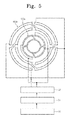
- FIG. 3A is a diagram schematically illustrating an antenna structure according to still another embodiment of the present invention.
- FIG. 3B is a cross-sectional view of an antenna structure of FIG. 3A .
- the antenna structure 100 a may include four induction antennas 101 a which have the same structure, are connected in parallel with one another, and are disposed to be overlapped.
- the induction antennas 101 a may include an external upper section 110 a disposed on a first quadrant of a first layer 141 ; an internal upper section 112 a connected to the external upper section 110 a and disposed on a second quadrant of a second layer 142 disposed at an upper part of the first layer; an internal lower section 122 a connected to the internal upper section 112 a and disposed on a third quadrant of a third layer 143 disposed at a lower part of the second layer; and an external lower section 120 a connected to the internal lower section 112 a and disposed on a fourth quadrant of a fourth layer 144 disposed at a lower part of the first layer 141 .
- One end of the external upper section 110 a may be supplied with an RF power, and the other end of the external lower section 120
- An upper branch 114 a may connect the other end of the external upper section 110 a and one end of the internal upper section 112 a .
- a vertical branch 130 a may connect the other end of the internal upper section 112 a and one end of the internal lower section 122 a .
- a lower branch 124 may connect the other end of the internal lower section 122 a and one end of the external lower section 120 a.
- FIG. 4 is a diagram schematically illustrating an antenna structure according to still another embodiment of the present invention.
- the antenna structure 300 may include two induction antennas 301 which have the same structure, are connected in parallel with one another, and are disposed to be overlapped.
- the induction antennas 301 may include an external upper section 310 disposed over a first quadrant and a second quadrant of a first layer; an internal upper section 312 connected to the external upper section 310 and disposed over a third quadrant and a fourth quadrant of the first layer; an internal lower section 322 connected to the internal upper section 312 and disposed over a first quadrant and a second quadrant of a second layer disposed at a lower part of the first layer; and an external lower section 320 connected to the internal lower section 322 and disposed over a third quadrant and a fourth quadrant of the second layer.
- One end of the external upper section 310 may be supplied with an RF power, and the other end of the external lower section 320 may be grounded.
- An upper branch 314 may connect the other end of the external upper section 310 and one end of the internal upper section 312 .
- a vertical branch 330 may connect the other end of the internal upper section 312 and one end of the internal lower section 322 .
- a lower branch 324 may connect the other end of the internal lower section 322 and one end of the external lower section 320 .
- FIG. 5 is a diagram schematically illustrating a plasma generating device according to an embodiment of the present invention.
- FIG. 6 is a cross-sectional view of a plasma generating device of FIG. 5 .
- a plasma generating device may include a vacuum container 50 , a dielectric unit 58 disposed at a part of the vacuum container 50 , and an antenna structure for plasma generation 400 a and 400 b disposed on the dielectric unit 58 .
- the antenna structure 400 a and 400 b may include a first antenna structure 400 a and a second antenna structure 400 b .
- the first antenna structure 400 a may be disposed in the second antenna structure 400 b.
- the first antenna structure 400 a and the second antenna structure 400 b may be connected to a power distribution unit 62 .
- the power distribution unit 62 may distribute a power to the first antenna structure 400 a and the second antenna structure 400 b .
- the power distribution unit 62 may be formed of passive elements such as inductors, capacitors, and so on.
- An RF power 66 may supply a power to the antenna structure 400 a and 400 b through an impedance matching network 64 and the power distribution unit 62 .
- the first antenna structure 400 a and the second antenna structure 400 b may be electrically connected in parallel.
- the antenna structure may include four induction antennas which have the same structure, are connected in parallel with one another, and are disposed to be overlapped.
- Each of the induction antennas may include an external upper section disposed on a first quadrant of a first layer; an internal upper section connected to the external upper section and disposed on a second quadrant of the first layer; an internal lower section connected to the internal upper section and disposed on a third quadrant of a second layer disposed at a lower part of the first layer; and an external lower section connected to the internal lower section and disposed on a fourth quadrant of the second layer.
- One end of the external upper section may be supplied with an RF power, and the other end of the external lower section may be grounded.
- FIG. 7 is a diagram schematically illustrating a plasma generating device according to another embodiment of the present invention.
- the plasma generating device may include a vacuum container 50 , a dielectric unit 58 a disposed at a part of the vacuum container 50 , and an antenna structure for plasma generation 100 disposed on the dielectric unit 58 a.
- the dielectric unit 58 a may include a plurality of dielectric portions spaced apart from one another.
- the antenna structure 100 may include a plurality of antenna structures spaced apart from one another. The antenna structures may be put on corresponding dielectric portions, respectively.
- the antenna structure may be changed with an antenna structure described with reference to FIGS. 1 to 4 .
Landscapes
- Physics & Mathematics (AREA)
- Engineering & Computer Science (AREA)
- Plasma & Fusion (AREA)
- Electromagnetism (AREA)
- Spectroscopy & Molecular Physics (AREA)
- Chemical & Material Sciences (AREA)
- Analytical Chemistry (AREA)
- Plasma Technology (AREA)
- Drying Of Semiconductors (AREA)
Abstract
An antenna structure includes four induction antennas which have the same structure, are connected in parallel and are disposed to be overlapped. The induction antennas include an external upper section arranged on a first quadrant of a first layer, an internal upper section connected to the external upper section and arranged on a second quadrant of the first layer, an internal lower section connected to the internal upper section and arranged on a third quadrant of a second layer arranged on a lower part of the first layer, and an external lower section connected to the internal lower section and arranged on a fourth quadrant of the second layer. An RF power is supplied to one end of the external upper section, and the other end of the external lower section is grounded.
Description
This is a divisional of U.S. application Ser. No. 13/990,840, filed on May 31, 2013, with a 371(c) date of Jul. 2, 2013, which is a National Phase of PCT/KR2011/006887, filed Sep. 16, 2011, the entire contents of each of which are hereby incorporated by reference.
The inventive concepts described herein relate to a plasma generating device, and more particularly, relate to an antenna structure capable of generating inductive coupling plasma
Large-scaled substrates such as a semiconductor substrate, a flat panel display substrate, a solar cell substrate, etc. may necessitate large-scaled fabricating devices for treating them. A plasma treatment device may be used for various processes such as etching, deposition, ion implantation, material surface treatment, etc.
The present invention provides an antenna structure capable of forming plasma uniformly.
The present invention also provides a plasma generating device capable of forming plasma uniformly.
The antenna structure includes four induction antennas which have the same structure, are connected in parallel and are disposed to be overlapped. The induction antennas include an external upper section disposed on a first quadrant of a first layer, an internal upper section connected to the external upper section and disposed on a second quadrant of the first layer, an internal lower section connected to the internal upper section and disposed on a third quadrant of a second layer disposed on a lower part of the first layer, and an external lower section connected to the internal lower section and disposed on a fourth quadrant of the second layer. An RF power is supplied to one end of the external upper section, and the other end of the external lower section is grounded.
With an embodiment of the present invention, an antenna structure provides inductive coupling plasma stably and uniformly.
A large-scaled plasma treatment device has to secure high plasma density, uniformity of plasma density, and process repeatability. Inductive coupling plasma may obtain high plasma. However, it is difficult to secure uniformity of plasma.
The present invention will now be described in detail with reference to the accompanying drawings, in which preferred embodiments of the invention are shown. However, the inventive concept is not limited thereto. Rather, embodiments introduced here may be provided such that disclosed contents become thorough and perfect and the spirit of the present invention is sufficiently provided to one skilled in the art. In figures, thickness of layers (or, films) and areas may be exaggeratedly illustrated. Also, in a case where a layer (or, film) is described to be put “on” another layer (or, film) or a substrate, a layer (or, film) may be directly put on another layer (or, film) or a substrate or on another layer (or, film) or a substrate with a third layer (or, film) interposed therebetween. Portions marked by the same reference numbers over the specification may indicate the same constituent elements.
Referring to FIGS. 1A to 1C , the antenna structure 100 may include four induction antennas 101 which have the same structure, are connected in parallel with one another, and are disposed to be overlapped. Each of the induction antennas 101 may include an external upper section 110 disposed on a first quadrant of a first layer; an internal upper section 112 connected to the external upper section 110 and disposed on a second quadrant of the first layer; an internal lower section 122 connected to the internal upper section 112 and disposed on a third quadrant of a second layer disposed at a lower part of the first layer; and an external lower section 120 connected to the internal lower section 122 and disposed on a fourth quadrant of the second layer. One ends P1, P2, P3, and P4 of the external upper sections 110 may be supplied with an RF power, and the other ends G1, G2, G3, and G4 of the external lower sections 120 may be grounded. The induction antennas 101 may be rotated by 90 degrees with respect to a central axis to be overlapped with one another.
In the antenna structure 100 according to an embodiment of the present invention, four induction antennas 101 may be electrically connected in parallel with one another. This may allow the antenna structure 100 to have low impedance, so that a high current is applied. Also, each of the induction antennas 101 may be interconnected without disconnection to form a loop. In this case, the induction antennas 101 may substantially form a closed loop to generate a maximal inducted electromotive force. A symmetrical shape of the antenna structure 100 may enable a symmetrical property of plasma in a rotation direction to be improved. Also, external sections 110 and 120 may form plasma outside, and the internal sections 112 and 122 may form plasma inside. Thus, radial uniformity of plasma may be improved.
The induction antennas 101 may be supplied with the RF power at the first layer and grounded at the second layer. Also, a current may flow through the induction antennas 101 in one direction such as a clockwise direction or counterclockwise direction. Thus, with the bi-level structure, it is possible to suppress such a phenomenon that a plasma density is locally increased due to capacitive coupling and inductive coupling at a location where the RF power is supplied.
The external upper section 110 may have a first curvature radius, and may be disposed at the first quadrant of the first layer. The external upper section 110 may have a metal or metal alloy strip or pipe shape. Desirably, the external upper section 110 may be formed of silver or gold plated copper. The external upper section 110 may have a thickness ranging from several millimeters to dozens millimeters. Desirably, the external upper section 110 may have a thickness ranging from 10 millimeters to 20 millimeters. The external upper section 110 can have a thickness of about several millimeters. One end of the external upper section 110 may be supplied with the RF power. The external upper sections 110 may be symmetrically disposed to form a peripheral area.
The internal upper section 112 may have a second curvature radius, and may be disposed on the second quadrant at substantially the same plane as the first layer. The internal upper section 112 may be disposed in an area which is formed by the external upper sections 110. The first curvature radius may be more than the second curvature radius. A current may flow into the induction antenna 101 in a clockwise direction. The internal upper sections 112 may be adjacent to the external upper sections, and may be disposed continuously in a rotation direction.
An upper branch 114 may connect the other end of the external upper section 110 and one end of the internal upper section 112. The upper branch 114 may be formed of the same material as that of the external upper section 110. The upper branch 114 and the external upper section 110 may be connected by electric connection means such as bolts and/or welding. The upper branch 114 and the internal upper section 112 may be connected by electric connection means such as bolts and/or welding.
A vertical branch 130 may connect the other end of the internal upper section 112 and one end of the internal lower section 122. The vertical branch 130 may connect the first layer and the second layer.
The internal lower sections 122 may be adjacent to the internal upper sections 112, and may be disposed continuously in a rotation direction.
The internal lower section 122 may be disposed at the second layer disposed under the first layer. The internal lower section 122 may be disposed on the third quadrant. An interval between the first layer and the second layer may be several millimeters to dozens millimeters. Desirably, an interval between the first layer and the second layer may be 10 millimeters to 15 millimeters. The internal lower section 122 may have the second curvature radius. An insulator 103 may be disposed between the first layer and the second layer.
A lower branch 124 may connect the other end of the internal lower section 122 and one end of the external lower section 120.
The external lower section 120 may be disposed on the fourth quadrant of the second layer. The external lower section 120 may have the first curvature radius. The other end of the external lower section 120 may be grounded.
Widths of the internal lower and upper sections 122 and 112 may be wider than those of the external lower and upper sections 120 and 110. Thus, a plasma generation space formed by the external upper section 110 and the external lower section 120 may be reduced, and a plasma generation space formed by the internal upper section 112 and the internal lower section 122 may be increased. This may mean that plasma uniformity in a radial direction increases.
To form large area plasma according to a large scaled plasma generating device, the RF power supplied to the antenna structure may run to nearly several KW to dozens KW. Also, divice's simplicity may be required. In recent years, to form large area plasma according to a large scaled plasma generating device, the RF power supplied to the antenna structure may run to nearly several KW to dozens KW. Thus, cooling may be required for thermal stability of the antenna structure 100. Also, device's simplicity may be required. Thus, the induction antennas 101 may have a pipe shape, and may be cooled by refrigerant such as air or fluid. The refrigerant may flow through insides of the induction antennas 101.
Referring to FIGS. 2A to 2C , the antenna structure 200 may include four induction antennas 201 which have the same structure, are connected in parallel with one another, and are disposed to be overlapped. Each of the induction antennas 201 may include an external upper section 210 disposed on a first quadrant of a first layer; an internal upper section 212 connected to the external upper section 210 and disposed on a second quadrant of the first layer; an internal lower section 222 connected to the internal upper section 212 and disposed on a third quadrant of a second layer disposed at a lower part of the first layer; and an external lower section 220 connected to the internal lower section 222 and disposed on a fourth quadrant of the second layer. One ends P1, P2, P3, and P4 of the external upper sections 210 may be supplied with an RF power, and the other ends G1, G2, G3, and G4 of the external lower sections 220 may be grounded. The induction antennas 201 may be rotated by 90 degrees with respect to a central axis to be overlapped with one another.
In the antenna structure 200 according to an embodiment of the present invention, four induction antennas 201 may be electrically connected in parallel with one another. This may allow the antenna structure 200 to have low impedance, so that a high current is applied. Also, each of the induction antennas 201 may be interconnected without disconnection to form a loop. In this case, the induction antennas 201 may substantially form a closed loop to generate a maximal inducted electromotive force. A symmetrical shape of the antenna structure 200 may enable a symmetrical property of plasma in a rotation direction to be improved. Also, the external sections 210 and 220 may form plasma outside, and the internal sections 212 and 222 may form plasma inside. Thus, radial uniformity of plasma may be improved.
The induction antennas 201 may be supplied with the RF power at the first layer and grounded at the second layer. Also, a current may flow through the induction antennas 201 in one direction such as a clockwise direction or counterclockwise direction. Thus, with the bi-level structure, it is possible to suppress such a phenomenon that a plasma density is locally increased due to capacitive coupling and inductive coupling at a location where the RF power is supplied.
The external upper section 210 may be bent at a right angle, and may be disposed on the first quadrant of the first layer. The external upper section 210 may have a metal or metal alloy strip or pipe shape. Desirably, the external upper section 210 may be formed of silver or gold plated copper. The external upper section 210 may have a thickness ranging from several millimeters to dozens millimeters. Desirably, the external upper section 210 may have a thickness ranging from 10 millimeters to 20 millimeters. The external upper section 210 can have a thickness of about several millimeters. One end of the external upper section 210 may be supplied with the RF power. The external upper sections 210 may be symmetrically disposed to form a peripheral area.
The internal upper section 212 may be bent at a right angle, and may be disposed on the second quadrant at substantially the same plane as the first layer. The internal upper section 212 may be disposed in an area which is formed by the external upper sections 210. An area occupied by the internal upper section 212 may be wider than an area occupied by the external upper section 210. A current may flow into the induction antenna 201 in a clockwise direction. The internal upper sections 212 may be adjacent to the external upper sections, and may be disposed continuously in a rotation direction.
An upper branch 214 may connect the other end of the external upper section 210 and one end of the internal upper section 212. The upper branch 214 may be formed of the same material as that of the external upper section 210. The upper branch 214 and the external upper section 210 may be connected by electric connection means such as bolts and/or welding. The upper branch 214 and the internal upper section 212 may be connected by electric connection means such as bolts and/or welding.
A vertical branch 230 may connect the other end of the internal upper section 212 and one end of the internal lower section 222. The vertical branch 230 may connect the first layer and the second layer.
The internal lower sections 222 may be adjacent to the internal upper sections 212, and may be disposed continuously in a rotation direction. The internal lower section 222 may be disposed at the second layer disposed under the first layer. The internal lower section 222 may be disposed on the third quadrant. An interval between the first layer and the second layer may be several millimeters to dozens millimeters. Desirably, an interval between the first layer and the second layer may be 10 millimeters to 15 millimeters. The internal lower section 222 may be bent at a right angle.
A lower branch 224 may connect the other end of the internal lower section 222 and one end of the external lower section 220.
The external lower section 220 may be disposed on the fourth quadrant of the second layer. The external lower section 220 may be bent at a right angle. The other end of the external lower section 220 may be grounded.
Widths of the internal lower and upper sections 222 and 212 may be wider than those of the external lower and upper sections 220 and 210. Thus, a plasma generation space formed by the external upper section 210 and the external lower section 220 may be reduced, and a plasma generation space formed by the internal upper section 212 and the internal lower section 222 may be increased. This may mean that plasma uniformity in a radial direction increases.
Referring to FIGS. 3A and 3B , the antenna structure 100 a may include four induction antennas 101 a which have the same structure, are connected in parallel with one another, and are disposed to be overlapped. the induction antennas 101 a may include an external upper section 110 a disposed on a first quadrant of a first layer 141; an internal upper section 112 a connected to the external upper section 110 a and disposed on a second quadrant of a second layer 142 disposed at an upper part of the first layer; an internal lower section 122 a connected to the internal upper section 112 a and disposed on a third quadrant of a third layer 143 disposed at a lower part of the second layer; and an external lower section 120 a connected to the internal lower section 112 a and disposed on a fourth quadrant of a fourth layer 144 disposed at a lower part of the first layer 141. One end of the external upper section 110 a may be supplied with an RF power, and the other end of the external lower section 120 a may be grounded.
An upper branch 114 a may connect the other end of the external upper section 110 a and one end of the internal upper section 112 a. A vertical branch 130 a may connect the other end of the internal upper section 112 a and one end of the internal lower section 122 a. A lower branch 124 may connect the other end of the internal lower section 122 a and one end of the external lower section 120 a.
Referring to FIG. 4 , the antenna structure 300 may include two induction antennas 301 which have the same structure, are connected in parallel with one another, and are disposed to be overlapped. the induction antennas 301 may include an external upper section 310 disposed over a first quadrant and a second quadrant of a first layer; an internal upper section 312 connected to the external upper section 310 and disposed over a third quadrant and a fourth quadrant of the first layer; an internal lower section 322 connected to the internal upper section 312 and disposed over a first quadrant and a second quadrant of a second layer disposed at a lower part of the first layer; and an external lower section 320 connected to the internal lower section 322 and disposed over a third quadrant and a fourth quadrant of the second layer. One end of the external upper section 310 may be supplied with an RF power, and the other end of the external lower section 320 may be grounded.
An upper branch 314 may connect the other end of the external upper section 310 and one end of the internal upper section 312. A vertical branch 330 may connect the other end of the internal upper section 312 and one end of the internal lower section 322. A lower branch 324 may connect the other end of the internal lower section 322 and one end of the external lower section 320.
The first antenna structure 400 a and the second antenna structure 400 b may be connected to a power distribution unit 62. The power distribution unit 62 may distribute a power to the first antenna structure 400 a and the second antenna structure 400 b. The power distribution unit 62 may be formed of passive elements such as inductors, capacitors, and so on.
An RF power 66 may supply a power to the antenna structure 400 a and 400 b through an impedance matching network 64 and the power distribution unit 62. The first antenna structure 400 a and the second antenna structure 400 b may be electrically connected in parallel. The antenna structure may include four induction antennas which have the same structure, are connected in parallel with one another, and are disposed to be overlapped. Each of the induction antennas may include an external upper section disposed on a first quadrant of a first layer; an internal upper section connected to the external upper section and disposed on a second quadrant of the first layer; an internal lower section connected to the internal upper section and disposed on a third quadrant of a second layer disposed at a lower part of the first layer; and an external lower section connected to the internal lower section and disposed on a fourth quadrant of the second layer. One end of the external upper section may be supplied with an RF power, and the other end of the external lower section may be grounded.
Referring to FIG. 7 , the plasma generating device may include a vacuum container 50, a dielectric unit 58 a disposed at a part of the vacuum container 50, and an antenna structure for plasma generation 100 disposed on the dielectric unit 58 a.
The dielectric unit 58 a may include a plurality of dielectric portions spaced apart from one another. The antenna structure 100 may include a plurality of antenna structures spaced apart from one another. The antenna structures may be put on corresponding dielectric portions, respectively.
With a modified embodiment of the present invention, the antenna structure may be changed with an antenna structure described with reference to FIGS. 1 to 4 .
Claims (2)
1. An antenna structure for plasma generation, comprising:
two induction antennas which have the same structure, are connected in parallel with one another, and are disposed to be overlapped,
wherein the induction antennas comprises:
an external upper section disposed over a first quadrant and a second quadrant of a first layer;
an internal upper section connected to the external upper section and disposed over a third quadrant and a fourth quadrant of the first layer;
an internal lower section connected to the internal upper section and disposed over a first quadrant and a second quadrant of a second layer disposed at a lower part of the first layer; and
an external lower section connected to the internal lower section and disposed over a third quadrant and a fourth quadrant of the second layer,
wherein one end of the external upper section is supplied with an RF power, and the other end of the external lower section is grounded.
2. The antenna structure of claim 1 , further comprising:
an upper branch connecting the other end of the external upper section and one end of the internal upper section;
a vertical branch connecting the other end of the internal upper section and one end of the internal lower section; and
a lower branch connecting the other end of the internal lower section and one end of the external lower section.
Priority Applications (1)
| Application Number | Priority Date | Filing Date | Title |
|---|---|---|---|
| US15/010,338 US9894745B2 (en) | 2011-09-16 | 2016-01-29 | Antenna structure and plasma generating device |
Applications Claiming Priority (3)
| Application Number | Priority Date | Filing Date | Title |
|---|---|---|---|
| PCT/KR2011/006887 WO2013039274A1 (en) | 2011-09-16 | 2011-09-16 | Antenna structure and plasma generating device |
| US201313990840A | 2013-07-02 | 2013-07-02 | |
| US15/010,338 US9894745B2 (en) | 2011-09-16 | 2016-01-29 | Antenna structure and plasma generating device |
Related Parent Applications (2)
| Application Number | Title | Priority Date | Filing Date |
|---|---|---|---|
| PCT/KR2011/006887 Division WO2013039274A1 (en) | 2011-09-16 | 2011-09-16 | Antenna structure and plasma generating device |
| US13/990,840 Division US9282624B2 (en) | 2011-09-16 | 2011-09-16 | Antenna structure and plasma generating device |
Publications (2)
| Publication Number | Publication Date |
|---|---|
| US20160150628A1 US20160150628A1 (en) | 2016-05-26 |
| US9894745B2 true US9894745B2 (en) | 2018-02-13 |
Family
ID=47883479
Family Applications (3)
| Application Number | Title | Priority Date | Filing Date |
|---|---|---|---|
| US13/990,840 Active 2032-08-24 US9282624B2 (en) | 2011-09-16 | 2011-09-16 | Antenna structure and plasma generating device |
| US15/010,440 Active US9642238B2 (en) | 2011-09-16 | 2016-01-29 | Antenna structure and plasma generating device |
| US15/010,338 Active US9894745B2 (en) | 2011-09-16 | 2016-01-29 | Antenna structure and plasma generating device |
Family Applications Before (2)
| Application Number | Title | Priority Date | Filing Date |
|---|---|---|---|
| US13/990,840 Active 2032-08-24 US9282624B2 (en) | 2011-09-16 | 2011-09-16 | Antenna structure and plasma generating device |
| US15/010,440 Active US9642238B2 (en) | 2011-09-16 | 2016-01-29 | Antenna structure and plasma generating device |
Country Status (4)
| Country | Link |
|---|---|
| US (3) | US9282624B2 (en) |
| KR (1) | KR101853370B1 (en) |
| CN (1) | CN103959920B (en) |
| WO (1) | WO2013039274A1 (en) |
Families Citing this family (16)
| Publication number | Priority date | Publication date | Assignee | Title |
|---|---|---|---|---|
| KR101853370B1 (en) * | 2011-09-16 | 2018-04-30 | 세메스 주식회사 | Antenna structure and plasma generating device |
| KR101874901B1 (en) | 2011-12-07 | 2018-07-06 | 삼성전자주식회사 | Apparatus and method for drying substrate |
| ES2873228T3 (en) * | 2013-02-11 | 2021-11-03 | Univ California | Winding for fractional turn coils |
| KR101714405B1 (en) * | 2015-07-29 | 2017-03-10 | 주식회사 윈텔 | Plasma processing apparatus |
| KR101714406B1 (en) * | 2015-08-04 | 2017-03-23 | 주식회사 윈텔 | Plasma Processing Apparatus |
| KR101714407B1 (en) * | 2015-08-04 | 2017-03-10 | 주식회사 윈텔 | Plasma Processing Apparatus |
| GB2541214A (en) * | 2015-08-12 | 2017-02-15 | Edwards Ltd | Plasma generator |
| KR102175253B1 (en) * | 2016-11-07 | 2020-11-06 | 윈텔코퍼레이션 주식회사 | Plasma Processing Apparatus |
| KR102175238B1 (en) * | 2016-11-07 | 2020-11-06 | 윈텔코퍼레이션 주식회사 | Plasma Processing Apparatus |
| KR101866212B1 (en) * | 2016-11-16 | 2018-06-12 | 인베니아 주식회사 | Plasma processing apparatus |
| JP7225058B2 (en) * | 2019-08-19 | 2023-02-20 | 株式会社東芝 | High frequency antenna and plasma processing equipment |
| JP7403348B2 (en) * | 2020-02-21 | 2023-12-22 | 東京エレクトロン株式会社 | Antenna segment and inductively coupled plasma processing equipment |
| WO2022146648A1 (en) * | 2020-12-28 | 2022-07-07 | Mattson Technology, Inc. | Induction coil assembly for plasma processing apparatus |
| US12451327B2 (en) | 2022-02-03 | 2025-10-21 | Tokyo Electron Limited | Apparatus for plasma processing |
| CN120188254A (en) * | 2022-11-09 | 2025-06-20 | 源多可科技股份有限公司 | Antenna structure |
| KR102844223B1 (en) * | 2022-12-15 | 2025-08-08 | 세메스 주식회사 | Substrate processing apparatus and plasma density control method |
Citations (13)
| Publication number | Priority date | Publication date | Assignee | Title |
|---|---|---|---|---|
| JPH08195296A (en) | 1995-01-13 | 1996-07-30 | Matsushita Electric Ind Co Ltd | Plasma processing device |
| CN1423827A (en) | 1999-11-15 | 2003-06-11 | 兰姆研究有限公司 | Method and apparatus for producing a uniform processing rate |
| CN1481207A (en) | 2002-09-04 | 2004-03-10 | ���ǵ�����ʽ���� | Inductively coupled plasma generator combined with double-layer coil antenna |
| CN1537405A (en) | 2001-07-30 | 2004-10-13 | 株式会社普来马特 | Inductively Coupled Plasma Generator Antenna Structure |
| KR100692420B1 (en) | 2005-12-09 | 2007-03-13 | 주식회사 플라즈마트 | Antenna Structure of Inductively Coupled Plasma Generator |
| KR20070033222A (en) | 2005-09-21 | 2007-03-26 | 주성엔지니어링(주) | Plasma Generating Antenna |
| KR20080107758A (en) | 2007-06-08 | 2008-12-11 | 참앤씨(주) | Inductively Coupled Plasma Treatment Apparatus and Antenna |
| KR20090027479A (en) | 2007-09-12 | 2009-03-17 | 한양대학교 산학협력단 | Antenna unit for plasma generation |
| CN101543141A (en) | 2006-11-28 | 2009-09-23 | 莎姆克株式会社 | Plasma processing apparatus |
| KR20090102257A (en) | 2008-03-25 | 2009-09-30 | (주)타이닉스 | Inductively coupled plasma etching apparatus |
| KR20110114118A (en) | 2010-04-13 | 2011-10-19 | 이용관 | Antenna Structure and Plasma Generator |
| US8712323B2 (en) | 2008-04-21 | 2014-04-29 | Tagarray, Inc. | Inductive antenna coupling |
| US9282624B2 (en) * | 2011-09-16 | 2016-03-08 | Semes Co., Ltd. | Antenna structure and plasma generating device |
Family Cites Families (12)
| Publication number | Priority date | Publication date | Assignee | Title |
|---|---|---|---|---|
| KR100338057B1 (en) * | 1999-08-26 | 2002-05-24 | 황 철 주 | Antenna device for generating inductively coupled plasma |
| US6518705B2 (en) * | 1999-11-15 | 2003-02-11 | Lam Research Corporation | Method and apparatus for producing uniform process rates |
| KR20010108968A (en) * | 2000-06-01 | 2001-12-08 | 황 철 주 | Plasma processing apparatus |
| US7294563B2 (en) * | 2000-08-10 | 2007-11-13 | Applied Materials, Inc. | Semiconductor on insulator vertical transistor fabrication and doping process |
| US7094316B1 (en) * | 2000-08-11 | 2006-08-22 | Applied Materials, Inc. | Externally excited torroidal plasma source |
| US6664548B2 (en) * | 2002-05-01 | 2003-12-16 | Axcelis Technologies, Inc. | Ion source and coaxial inductive coupler for ion implantation system |
| JP3823069B2 (en) * | 2002-06-12 | 2006-09-20 | 株式会社アルバック | Magnetic neutral discharge plasma processing equipment |
| JP4302630B2 (en) * | 2002-07-26 | 2009-07-29 | プラズマート カンパニー リミテッド | Inductively coupled plasma generator |
| KR101007822B1 (en) * | 2003-07-14 | 2011-01-13 | 주성엔지니어링(주) | Mixed Plasma Generator |
| TWI498053B (en) * | 2008-12-23 | 2015-08-21 | Ind Tech Res Inst | Plasma excitation module |
| JP5870568B2 (en) * | 2011-05-12 | 2016-03-01 | 東京エレクトロン株式会社 | Film forming apparatus, plasma processing apparatus, film forming method, and storage medium |
| US8933628B2 (en) * | 2011-10-28 | 2015-01-13 | Applied Materials, Inc. | Inductively coupled plasma source with phase control |
-
2011
- 2011-09-16 KR KR1020147001265A patent/KR101853370B1/en active Active
- 2011-09-16 US US13/990,840 patent/US9282624B2/en active Active
- 2011-09-16 CN CN201180073518.2A patent/CN103959920B/en active Active
- 2011-09-16 WO PCT/KR2011/006887 patent/WO2013039274A1/en not_active Ceased
-
2016
- 2016-01-29 US US15/010,440 patent/US9642238B2/en active Active
- 2016-01-29 US US15/010,338 patent/US9894745B2/en active Active
Patent Citations (14)
| Publication number | Priority date | Publication date | Assignee | Title |
|---|---|---|---|---|
| JPH08195296A (en) | 1995-01-13 | 1996-07-30 | Matsushita Electric Ind Co Ltd | Plasma processing device |
| CN1423827A (en) | 1999-11-15 | 2003-06-11 | 兰姆研究有限公司 | Method and apparatus for producing a uniform processing rate |
| CN1537405A (en) | 2001-07-30 | 2004-10-13 | 株式会社普来马特 | Inductively Coupled Plasma Generator Antenna Structure |
| CN1481207A (en) | 2002-09-04 | 2004-03-10 | ���ǵ�����ʽ���� | Inductively coupled plasma generator combined with double-layer coil antenna |
| KR20070033222A (en) | 2005-09-21 | 2007-03-26 | 주성엔지니어링(주) | Plasma Generating Antenna |
| KR100692420B1 (en) | 2005-12-09 | 2007-03-13 | 주식회사 플라즈마트 | Antenna Structure of Inductively Coupled Plasma Generator |
| CN101543141A (en) | 2006-11-28 | 2009-09-23 | 莎姆克株式会社 | Plasma processing apparatus |
| KR20080107758A (en) | 2007-06-08 | 2008-12-11 | 참앤씨(주) | Inductively Coupled Plasma Treatment Apparatus and Antenna |
| KR20090027479A (en) | 2007-09-12 | 2009-03-17 | 한양대학교 산학협력단 | Antenna unit for plasma generation |
| KR20090102257A (en) | 2008-03-25 | 2009-09-30 | (주)타이닉스 | Inductively coupled plasma etching apparatus |
| US8712323B2 (en) | 2008-04-21 | 2014-04-29 | Tagarray, Inc. | Inductive antenna coupling |
| KR20110114118A (en) | 2010-04-13 | 2011-10-19 | 이용관 | Antenna Structure and Plasma Generator |
| US9282624B2 (en) * | 2011-09-16 | 2016-03-08 | Semes Co., Ltd. | Antenna structure and plasma generating device |
| US9642238B2 (en) * | 2011-09-16 | 2017-05-02 | Semes Co., Ltd. | Antenna structure and plasma generating device |
Non-Patent Citations (1)
| Title |
|---|
| International Search Report PCT/ISA/210 for PCT/KR2011/006887 dated Feb. 15, 2012. |
Also Published As
| Publication number | Publication date |
|---|---|
| US20130278136A1 (en) | 2013-10-24 |
| US9642238B2 (en) | 2017-05-02 |
| US20160150629A1 (en) | 2016-05-26 |
| US9282624B2 (en) | 2016-03-08 |
| CN103959920A (en) | 2014-07-30 |
| WO2013039274A1 (en) | 2013-03-21 |
| US20160150628A1 (en) | 2016-05-26 |
| KR20140063568A (en) | 2014-05-27 |
| KR101853370B1 (en) | 2018-04-30 |
| CN103959920B (en) | 2016-12-07 |
Similar Documents
| Publication | Publication Date | Title |
|---|---|---|
| US9894745B2 (en) | Antenna structure and plasma generating device | |
| US8917022B2 (en) | Plasma generation device and plasma processing device | |
| TWI885502B (en) | Antenna structure and plasma generating apparatus | |
| JP3987033B2 (en) | Antenna structure of inductively coupled plasma generator | |
| TWI590373B (en) | Substrate holder with symmetric supply structure | |
| WO2001019144A1 (en) | Inner-electrode plasma processing apparatus and method of plasma processing | |
| CN105491780A (en) | Antenna for plasma generation and plasma processing device having the same | |
| US20110120375A1 (en) | Apparatus for processing substrate | |
| US12394594B2 (en) | Inductive coil structure and inductively coupled plasma generation system | |
| US11456154B2 (en) | Plasma-generating unit and substrate treatment apparatus including the same | |
| CN103811262B (en) | Inductance coupling plasma processing device | |
| KR101125624B1 (en) | Antenna structure and plasma generation apparatus | |
| KR20100129368A (en) | Plasma reactor using multi-frequency | |
| KR100692420B1 (en) | Antenna Structure of Inductively Coupled Plasma Generator | |
| TWI406336B (en) | High density plasma generator | |
| KR101598175B1 (en) | Antenna structure and plasma generation apparatus | |
| CN102859665A (en) | Plasma processing apparatus | |
| JP2003077902A (en) | Plasma generator | |
| KR101104093B1 (en) | Internal Antenna and Plasma Generator | |
| TWI908765B (en) | Inductively coupled antenna and plasma treatment device | |
| TWI917258B (en) | Antenna structure and plasma generating apparatus | |
| KR20070032758A (en) | Antenna for inductive coupled plasma generating apparatus | |
| KR20240169287A (en) | Substrate Processing Apparatus |
Legal Events
| Date | Code | Title | Description |
|---|---|---|---|
| STCF | Information on status: patent grant |
Free format text: PATENTED CASE |
|
| MAFP | Maintenance fee payment |
Free format text: PAYMENT OF MAINTENANCE FEE, 4TH YEAR, LARGE ENTITY (ORIGINAL EVENT CODE: M1551); ENTITY STATUS OF PATENT OWNER: LARGE ENTITY Year of fee payment: 4 |
|
| MAFP | Maintenance fee payment |
Free format text: PAYMENT OF MAINTENANCE FEE, 8TH YEAR, LARGE ENTITY (ORIGINAL EVENT CODE: M1552); ENTITY STATUS OF PATENT OWNER: LARGE ENTITY Year of fee payment: 8 |