US9881663B2 - Stacked semiconductor device - Google Patents
Stacked semiconductor device Download PDFInfo
- Publication number
- US9881663B2 US9881663B2 US15/175,933 US201615175933A US9881663B2 US 9881663 B2 US9881663 B2 US 9881663B2 US 201615175933 A US201615175933 A US 201615175933A US 9881663 B2 US9881663 B2 US 9881663B2
- Authority
- US
- United States
- Prior art keywords
- memory
- data
- circuit
- chip
- point
- Prior art date
- Legal status (The legal status is an assumption and is not a legal conclusion. Google has not performed a legal analysis and makes no representation as to the accuracy of the status listed.)
- Active
Links
Images
Classifications
-
- G—PHYSICS
- G11—INFORMATION STORAGE
- G11C—STATIC STORES
- G11C11/00—Digital stores characterised by the use of particular electric or magnetic storage elements; Storage elements therefor
- G11C11/21—Digital stores characterised by the use of particular electric or magnetic storage elements; Storage elements therefor using electric elements
- G11C11/34—Digital stores characterised by the use of particular electric or magnetic storage elements; Storage elements therefor using electric elements using semiconductor devices
- G11C11/40—Digital stores characterised by the use of particular electric or magnetic storage elements; Storage elements therefor using electric elements using semiconductor devices using transistors
- G11C11/401—Digital stores characterised by the use of particular electric or magnetic storage elements; Storage elements therefor using electric elements using semiconductor devices using transistors forming cells needing refreshing or charge regeneration, i.e. dynamic cells
- G11C11/4063—Auxiliary circuits, e.g. for addressing, decoding, driving, writing, sensing or timing
- G11C11/407—Auxiliary circuits, e.g. for addressing, decoding, driving, writing, sensing or timing for memory cells of the field-effect type
- G11C11/409—Read-write [R-W] circuits
- G11C11/4093—Input/output [I/O] data interface arrangements, e.g. data buffers
-
- G—PHYSICS
- G11—INFORMATION STORAGE
- G11C—STATIC STORES
- G11C11/00—Digital stores characterised by the use of particular electric or magnetic storage elements; Storage elements therefor
- G11C11/21—Digital stores characterised by the use of particular electric or magnetic storage elements; Storage elements therefor using electric elements
- G11C11/34—Digital stores characterised by the use of particular electric or magnetic storage elements; Storage elements therefor using electric elements using semiconductor devices
- G11C11/40—Digital stores characterised by the use of particular electric or magnetic storage elements; Storage elements therefor using electric elements using semiconductor devices using transistors
- G11C11/401—Digital stores characterised by the use of particular electric or magnetic storage elements; Storage elements therefor using electric elements using semiconductor devices using transistors forming cells needing refreshing or charge regeneration, i.e. dynamic cells
- G11C11/4063—Auxiliary circuits, e.g. for addressing, decoding, driving, writing, sensing or timing
- G11C11/407—Auxiliary circuits, e.g. for addressing, decoding, driving, writing, sensing or timing for memory cells of the field-effect type
- G11C11/409—Read-write [R-W] circuits
- G11C11/4096—Input/output [I/O] data management or control circuits, e.g. reading or writing circuits, I/O drivers or bit-line switches
-
- G—PHYSICS
- G11—INFORMATION STORAGE
- G11C—STATIC STORES
- G11C17/00—Read-only memories programmable only once; Semi-permanent stores, e.g. manually-replaceable information cards
- G11C17/14—Read-only memories programmable only once; Semi-permanent stores, e.g. manually-replaceable information cards in which contents are determined by selectively establishing, breaking or modifying connecting links by permanently altering the state of coupling elements, e.g. PROM
- G11C17/16—Read-only memories programmable only once; Semi-permanent stores, e.g. manually-replaceable information cards in which contents are determined by selectively establishing, breaking or modifying connecting links by permanently altering the state of coupling elements, e.g. PROM using electrically-fusible links
-
- G—PHYSICS
- G11—INFORMATION STORAGE
- G11C—STATIC STORES
- G11C17/00—Read-only memories programmable only once; Semi-permanent stores, e.g. manually-replaceable information cards
- G11C17/14—Read-only memories programmable only once; Semi-permanent stores, e.g. manually-replaceable information cards in which contents are determined by selectively establishing, breaking or modifying connecting links by permanently altering the state of coupling elements, e.g. PROM
- G11C17/18—Auxiliary circuits, e.g. for writing into memory
-
- G—PHYSICS
- G11—INFORMATION STORAGE
- G11C—STATIC STORES
- G11C5/00—Details of stores covered by group G11C11/00
- G11C5/02—Disposition of storage elements, e.g. in the form of a matrix array
- G11C5/04—Supports for storage elements, e.g. memory modules; Mounting or fixing of storage elements on such supports
-
- H—ELECTRICITY
- H01—ELECTRIC ELEMENTS
- H01L—SEMICONDUCTOR DEVICES NOT COVERED BY CLASS H10
- H01L25/00—Assemblies consisting of a plurality of individual semiconductor or other solid state devices ; Multistep manufacturing processes thereof
- H01L25/03—Assemblies consisting of a plurality of individual semiconductor or other solid state devices ; Multistep manufacturing processes thereof all the devices being of a type provided for in the same subgroup of groups H01L27/00 - H01L33/00, or in a single subclass of H10K, H10N, e.g. assemblies of rectifier diodes
- H01L25/04—Assemblies consisting of a plurality of individual semiconductor or other solid state devices ; Multistep manufacturing processes thereof all the devices being of a type provided for in the same subgroup of groups H01L27/00 - H01L33/00, or in a single subclass of H10K, H10N, e.g. assemblies of rectifier diodes the devices not having separate containers
- H01L25/065—Assemblies consisting of a plurality of individual semiconductor or other solid state devices ; Multistep manufacturing processes thereof all the devices being of a type provided for in the same subgroup of groups H01L27/00 - H01L33/00, or in a single subclass of H10K, H10N, e.g. assemblies of rectifier diodes the devices not having separate containers the devices being of a type provided for in group H01L27/00
- H01L25/0657—Stacked arrangements of devices
-
- H—ELECTRICITY
- H01—ELECTRIC ELEMENTS
- H01L—SEMICONDUCTOR DEVICES NOT COVERED BY CLASS H10
- H01L2224/00—Indexing scheme for arrangements for connecting or disconnecting semiconductor or solid-state bodies and methods related thereto as covered by H01L24/00
- H01L2224/01—Means for bonding being attached to, or being formed on, the surface to be connected, e.g. chip-to-package, die-attach, "first-level" interconnects; Manufacturing methods related thereto
- H01L2224/02—Bonding areas; Manufacturing methods related thereto
- H01L2224/04—Structure, shape, material or disposition of the bonding areas prior to the connecting process
- H01L2224/05—Structure, shape, material or disposition of the bonding areas prior to the connecting process of an individual bonding area
- H01L2224/0554—External layer
- H01L2224/0555—Shape
- H01L2224/05552—Shape in top view
-
- H—ELECTRICITY
- H01—ELECTRIC ELEMENTS
- H01L—SEMICONDUCTOR DEVICES NOT COVERED BY CLASS H10
- H01L2224/00—Indexing scheme for arrangements for connecting or disconnecting semiconductor or solid-state bodies and methods related thereto as covered by H01L24/00
- H01L2224/01—Means for bonding being attached to, or being formed on, the surface to be connected, e.g. chip-to-package, die-attach, "first-level" interconnects; Manufacturing methods related thereto
- H01L2224/02—Bonding areas; Manufacturing methods related thereto
- H01L2224/04—Structure, shape, material or disposition of the bonding areas prior to the connecting process
- H01L2224/05—Structure, shape, material or disposition of the bonding areas prior to the connecting process of an individual bonding area
- H01L2224/0554—External layer
- H01L2224/0556—Disposition
- H01L2224/05568—Disposition the whole external layer protruding from the surface
-
- H—ELECTRICITY
- H01—ELECTRIC ELEMENTS
- H01L—SEMICONDUCTOR DEVICES NOT COVERED BY CLASS H10
- H01L2224/00—Indexing scheme for arrangements for connecting or disconnecting semiconductor or solid-state bodies and methods related thereto as covered by H01L24/00
- H01L2224/01—Means for bonding being attached to, or being formed on, the surface to be connected, e.g. chip-to-package, die-attach, "first-level" interconnects; Manufacturing methods related thereto
- H01L2224/02—Bonding areas; Manufacturing methods related thereto
- H01L2224/07—Structure, shape, material or disposition of the bonding areas after the connecting process
- H01L2224/08—Structure, shape, material or disposition of the bonding areas after the connecting process of an individual bonding area
- H01L2224/081—Disposition
- H01L2224/0812—Disposition the bonding area connecting directly to another bonding area, i.e. connectorless bonding, e.g. bumpless bonding
- H01L2224/08135—Disposition the bonding area connecting directly to another bonding area, i.e. connectorless bonding, e.g. bumpless bonding the bonding area connecting between different semiconductor or solid-state bodies, i.e. chip-to-chip
- H01L2224/08145—Disposition the bonding area connecting directly to another bonding area, i.e. connectorless bonding, e.g. bumpless bonding the bonding area connecting between different semiconductor or solid-state bodies, i.e. chip-to-chip the bodies being stacked
- H01L2224/08148—Disposition the bonding area connecting directly to another bonding area, i.e. connectorless bonding, e.g. bumpless bonding the bonding area connecting between different semiconductor or solid-state bodies, i.e. chip-to-chip the bodies being stacked the bonding area connecting to a bonding area protruding from the surface of the body
-
- H—ELECTRICITY
- H01—ELECTRIC ELEMENTS
- H01L—SEMICONDUCTOR DEVICES NOT COVERED BY CLASS H10
- H01L2224/00—Indexing scheme for arrangements for connecting or disconnecting semiconductor or solid-state bodies and methods related thereto as covered by H01L24/00
- H01L2224/80—Methods for connecting semiconductor or other solid state bodies using means for bonding being attached to, or being formed on, the surface to be connected
- H01L2224/80001—Methods for connecting semiconductor or other solid state bodies using means for bonding being attached to, or being formed on, the surface to be connected by connecting a bonding area directly to another bonding area, i.e. connectorless bonding, e.g. bumpless bonding
- H01L2224/8012—Aligning
- H01L2224/80121—Active alignment, i.e. by apparatus steering, e.g. optical alignment using marks or sensors
- H01L2224/8013—Active alignment, i.e. by apparatus steering, e.g. optical alignment using marks or sensors using marks formed on the semiconductor or solid-state body
-
- H—ELECTRICITY
- H01—ELECTRIC ELEMENTS
- H01L—SEMICONDUCTOR DEVICES NOT COVERED BY CLASS H10
- H01L2224/00—Indexing scheme for arrangements for connecting or disconnecting semiconductor or solid-state bodies and methods related thereto as covered by H01L24/00
- H01L2224/80—Methods for connecting semiconductor or other solid state bodies using means for bonding being attached to, or being formed on, the surface to be connected
- H01L2224/80001—Methods for connecting semiconductor or other solid state bodies using means for bonding being attached to, or being formed on, the surface to be connected by connecting a bonding area directly to another bonding area, i.e. connectorless bonding, e.g. bumpless bonding
- H01L2224/8012—Aligning
- H01L2224/80121—Active alignment, i.e. by apparatus steering, e.g. optical alignment using marks or sensors
- H01L2224/80132—Active alignment, i.e. by apparatus steering, e.g. optical alignment using marks or sensors using marks formed outside the semiconductor or solid-state body, i.e. "off-chip"
-
- H—ELECTRICITY
- H01—ELECTRIC ELEMENTS
- H01L—SEMICONDUCTOR DEVICES NOT COVERED BY CLASS H10
- H01L2224/00—Indexing scheme for arrangements for connecting or disconnecting semiconductor or solid-state bodies and methods related thereto as covered by H01L24/00
- H01L2224/80—Methods for connecting semiconductor or other solid state bodies using means for bonding being attached to, or being formed on, the surface to be connected
- H01L2224/80001—Methods for connecting semiconductor or other solid state bodies using means for bonding being attached to, or being formed on, the surface to be connected by connecting a bonding area directly to another bonding area, i.e. connectorless bonding, e.g. bumpless bonding
- H01L2224/808—Bonding techniques
- H01L2224/80897—Mechanical interlocking, e.g. anchoring, hook and loop-type fastening or the like
-
- H—ELECTRICITY
- H01—ELECTRIC ELEMENTS
- H01L—SEMICONDUCTOR DEVICES NOT COVERED BY CLASS H10
- H01L2225/00—Details relating to assemblies covered by the group H01L25/00 but not provided for in its subgroups
- H01L2225/03—All the devices being of a type provided for in the same subgroup of groups H01L27/00 - H01L33/648 and H10K99/00
- H01L2225/04—All the devices being of a type provided for in the same subgroup of groups H01L27/00 - H01L33/648 and H10K99/00 the devices not having separate containers
- H01L2225/065—All the devices being of a type provided for in the same subgroup of groups H01L27/00 - H01L33/648 and H10K99/00 the devices not having separate containers the devices being of a type provided for in group H01L27/00
- H01L2225/06503—Stacked arrangements of devices
- H01L2225/06527—Special adaptation of electrical connections, e.g. rewiring, engineering changes, pressure contacts, layout
-
- H—ELECTRICITY
- H01—ELECTRIC ELEMENTS
- H01L—SEMICONDUCTOR DEVICES NOT COVERED BY CLASS H10
- H01L2225/00—Details relating to assemblies covered by the group H01L25/00 but not provided for in its subgroups
- H01L2225/03—All the devices being of a type provided for in the same subgroup of groups H01L27/00 - H01L33/648 and H10K99/00
- H01L2225/04—All the devices being of a type provided for in the same subgroup of groups H01L27/00 - H01L33/648 and H10K99/00 the devices not having separate containers
- H01L2225/065—All the devices being of a type provided for in the same subgroup of groups H01L27/00 - H01L33/648 and H10K99/00 the devices not having separate containers the devices being of a type provided for in group H01L27/00
- H01L2225/06503—Stacked arrangements of devices
- H01L2225/06541—Conductive via connections through the device, e.g. vertical interconnects, through silicon via [TSV]
-
- H—ELECTRICITY
- H01—ELECTRIC ELEMENTS
- H01L—SEMICONDUCTOR DEVICES NOT COVERED BY CLASS H10
- H01L24/00—Arrangements for connecting or disconnecting semiconductor or solid-state bodies; Methods or apparatus related thereto
- H01L24/01—Means for bonding being attached to, or being formed on, the surface to be connected, e.g. chip-to-package, die-attach, "first-level" interconnects; Manufacturing methods related thereto
- H01L24/02—Bonding areas ; Manufacturing methods related thereto
- H01L24/04—Structure, shape, material or disposition of the bonding areas prior to the connecting process
- H01L24/05—Structure, shape, material or disposition of the bonding areas prior to the connecting process of an individual bonding area
-
- H—ELECTRICITY
- H01—ELECTRIC ELEMENTS
- H01L—SEMICONDUCTOR DEVICES NOT COVERED BY CLASS H10
- H01L24/00—Arrangements for connecting or disconnecting semiconductor or solid-state bodies; Methods or apparatus related thereto
- H01L24/01—Means for bonding being attached to, or being formed on, the surface to be connected, e.g. chip-to-package, die-attach, "first-level" interconnects; Manufacturing methods related thereto
- H01L24/02—Bonding areas ; Manufacturing methods related thereto
- H01L24/07—Structure, shape, material or disposition of the bonding areas after the connecting process
- H01L24/08—Structure, shape, material or disposition of the bonding areas after the connecting process of an individual bonding area
-
- H—ELECTRICITY
- H01—ELECTRIC ELEMENTS
- H01L—SEMICONDUCTOR DEVICES NOT COVERED BY CLASS H10
- H01L24/00—Arrangements for connecting or disconnecting semiconductor or solid-state bodies; Methods or apparatus related thereto
- H01L24/80—Methods for connecting semiconductor or other solid state bodies using means for bonding being attached to, or being formed on, the surface to be connected
-
- H—ELECTRICITY
- H01—ELECTRIC ELEMENTS
- H01L—SEMICONDUCTOR DEVICES NOT COVERED BY CLASS H10
- H01L25/00—Assemblies consisting of a plurality of individual semiconductor or other solid state devices ; Multistep manufacturing processes thereof
- H01L25/18—Assemblies consisting of a plurality of individual semiconductor or other solid state devices ; Multistep manufacturing processes thereof the devices being of types provided for in two or more different subgroups of the same main group of groups H01L27/00 - H01L33/00, or in a single subclass of H10K, H10N
-
- H—ELECTRICITY
- H01—ELECTRIC ELEMENTS
- H01L—SEMICONDUCTOR DEVICES NOT COVERED BY CLASS H10
- H01L2924/00—Indexing scheme for arrangements or methods for connecting or disconnecting semiconductor or solid-state bodies as covered by H01L24/00
-
- H—ELECTRICITY
- H01—ELECTRIC ELEMENTS
- H01L—SEMICONDUCTOR DEVICES NOT COVERED BY CLASS H10
- H01L2924/00—Indexing scheme for arrangements or methods for connecting or disconnecting semiconductor or solid-state bodies as covered by H01L24/00
- H01L2924/0001—Technical content checked by a classifier
- H01L2924/00014—Technical content checked by a classifier the subject-matter covered by the group, the symbol of which is combined with the symbol of this group, being disclosed without further technical details
-
- H—ELECTRICITY
- H01—ELECTRIC ELEMENTS
- H01L—SEMICONDUCTOR DEVICES NOT COVERED BY CLASS H10
- H01L2924/00—Indexing scheme for arrangements or methods for connecting or disconnecting semiconductor or solid-state bodies as covered by H01L24/00
- H01L2924/0001—Technical content checked by a classifier
- H01L2924/0002—Not covered by any one of groups H01L24/00, H01L24/00 and H01L2224/00
-
- H—ELECTRICITY
- H01—ELECTRIC ELEMENTS
- H01L—SEMICONDUCTOR DEVICES NOT COVERED BY CLASS H10
- H01L2924/00—Indexing scheme for arrangements or methods for connecting or disconnecting semiconductor or solid-state bodies as covered by H01L24/00
- H01L2924/10—Details of semiconductor or other solid state devices to be connected
- H01L2924/102—Material of the semiconductor or solid state bodies
- H01L2924/1025—Semiconducting materials
- H01L2924/10251—Elemental semiconductors, i.e. Group IV
- H01L2924/10253—Silicon [Si]
-
- H—ELECTRICITY
- H01—ELECTRIC ELEMENTS
- H01L—SEMICONDUCTOR DEVICES NOT COVERED BY CLASS H10
- H01L2924/00—Indexing scheme for arrangements or methods for connecting or disconnecting semiconductor or solid-state bodies as covered by H01L24/00
- H01L2924/10—Details of semiconductor or other solid state devices to be connected
- H01L2924/11—Device type
- H01L2924/14—Integrated circuits
Definitions
- Semiconductor packaging often involves assembling and electrically interconnecting groups of semiconductor devices together in space-efficient, yet inexpensive ways.
- One packaging approach involves stacking devices to reduce the horizontal footprint of the assembled system.
- Conventional stacking schemes typically rely on signal redistribution layers and/or wire-bond resources to provide electrical access to and from each device.
- conventional stacking arrangements often overlook power efficiency concerns.
- FIG. 1 illustrates a three-dimensional exploded view of a packaged semiconductor system employing stacked devices in accordance with one embodiment of the disclosure herein;
- FIG. 2 illustrates a two-dimensional partial side view of the stacked device system of FIG. 1 with the pad and I/O circuitry for each device shown as if from a top plan view;
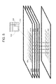
- FIG. 3 illustrates a partial cross-sectional view of two semiconductor devices showing formed vias employed in the system of FIG. 1 ;
- FIG. 4 illustrates a generalized top plan view of an alignment technique for offsetting the stacked semiconductor devices of FIG. 1 ;
- FIG. 5 illustrates a three-dimensional exploded view similar to FIG. 1 for an alternative embodiment
- FIG. 6 shows a two-dimensional partial side view similar to FIG. 2 for the alternative embodiment of FIG. 5 ;
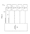
- FIG. 7 illustrates the routing of a serial bus used in one embodiment of the stacked semiconductor system of FIG. 5 to initialize one or more of the stacked semiconductor devices
- FIG. 8 shows one embodiment of a memory system employing point-to-point and multi-drop interconnection paths.
- Embodiments of systems and methods are described herein where a plurality of semiconductor devices employing through-silicon-vias are stacked to allow access of at least one of the semiconductor devices by way of through-silicon-vias in at least one other of the semiconductor devices.
- the through-silicon-vias are designed and device-aligned to reduce input/output (I/O) loading along a given via path.
- I/O input/output
- the system enables optimal point-to-point connections between I/O circuitry in a base device, and I/O circuitry in one of the plurality of devices. This, in turn, improves system speed and power efficiency.
- the through-silicon-vias in each of the plurality of semiconductor devices are arranged in an array.
- Each semiconductor device has two opposing surfaces and a corresponding pad array on each of the opposing surfaces.
- the reduced I/O loading is achieved by staggering I/O circuits among a pad array and offsetting adjacent devices by at least one pad location.
- the two adjacent devices are offset from each other by at least the distance between two adjacent columns of pads such that the first column of the through-silicon-via array in a first one of the adjacent devices are aligned with respective ones of the second column of the through-silicon-via array in the other one of the adjacent devices, the second column of the through-silicon-via array in the first one of the adjacent devices are aligned with respective ones of the third column of the through-silicon-via array in the other one of the adjacent devices, etc.
- the cooperation between the staggered I/O circuits and the offsetting between adjacent devices minimizes the number of I/O circuits coupled to each via path, resulting in reduced I/O loading thereof.
- the alignment is accomplished through a straight-up stack without offsetting.
- the I/O circuitry is not staggered, but rather selectively enabled to reduce the I/O loadings.
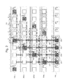
- FIGS. 1-3 illustrate respective three-dimensional and two-dimensional views for one specific embodiment of a semiconductor die stack 100 that facilitates point-to-point interconnections while reducing power dissipation and cost.
- a plurality of semiconductor dies 102 a - 102 d are provided for stacking.
- Each of the semiconductor dies 102 a - 102 d has oppositely disposed first and second surfaces 304 and 306 , a plurality of pads 308 formed on the first surface, a plurality of pads 308 formed on the second surface, and a plurality of through-vias 302 connecting respective pads on the first surface to respective pads on the second surface.
- the pads and vias are arranged in respective arrays, such as the array of pads 104 a - 104 d on the first surfaces.
- the arrays of pads 104 a - 104 d include I/O pads 112 (in magnified callout 110 ), which are pads coupled to corresponding I/O circuitry on the same die, and non-I/O pads, which are pads 111 not coupled to any I/O circuits on the same die.
- the array of through-vias in each semiconductor die would include a first group of through-vias coupled to respective I/O circuitry on the same semiconductor die and a second group of through-vias not coupled to I/O circuitry on the same semiconductor die.
- a processor die 108 preferably forms the base of the stack 100 , but may be remotely disposed therefrom as the application dictates.
- the processor device 108 accesses a die higher in the stack, such as die 102 c , by way of some of the through-vias in the same die and some of the through-vias in the dies lower in the stack, such as dies 102 a and 102 b , i.e., these vias form via paths for accessing the die 102 c .
- the processor device 108 optionally employs a via array (shown in phantom in FIG. 3 ) that may or may not correspond to the stacked die via arrays depending on whether the active circuitry on the processor device is facing the stack.
- each of the I/O pads 110 may take one of several forms. Generally, each pad represents the area occupied by the via structure (the via post diameter in addition to the surrounding metal pad) that couples to a corresponding via structure on an adjacent silicon die.
- each I/O pads 112 electrically couples to transmit and/or receiver circuits such as a driver/receiver pair (or transceiver) 114 , and possibly electro-static-discharge (ESD) circuitry (not shown) associated with the transmit and/or receive circuits, on the same die.
- An optional programmable mode register 116 provides a selectable enable/disable state for the driver/receiver circuitry.
- the capacitive coupling of this I/O circuit type may have the ability to load a via path with capacitance on the order of hundreds of femptofarads.
- the non-I/O pads 111 are employed.
- the non-I/O pads are pads not having any associated I/O circuitry (e.g., driver/transceiver pair and ESD circuitry).
- I/O circuitry e.g., driver/transceiver pair and ESD circuitry.
- FIG. 2 only one in every four pad locations (such as at 210 ) in a given row of pads 212 (in phantom) is formed with I/O circuitry, defining a staggered I/O circuit pattern. This allows for point-to-point connections between processor die 208 and up to four semiconductor dies 202 a - 202 d stacked above the processor die 208 .
- the point-to-point connectivity enables sizing of the I/O transceivers on the processor device for driving/receiving signals to/from one load (as opposed to multiple loads for a multi-drop configuration).
- the sizing may be in terms of current or voltage driving capability or the like. This, in turn, provides significant power savings, especially as the number of I/Os scale upwards for a given device stack.
- the via array generally reflects the array shape, size, and pitch exhibited by the pad array.
- each TSV 300 is formed to provide a conductive path 302 oriented orthogonally between the active surface of the die 304 and the backside surface of the die 306 .
- a raised pad structure 308 caps each via end.
- Pads disposed on the active surface of the die are generally formed coextensive with, and may actually define the I/O contact pads. Thus, for a given die, depending on the regular “stagger” of the I/O circuit pattern described above, a first set or group of vias will be coupled to I/O pads, while at least a portion of the rest (a second group) will be coupled to non-I/O pads on that die (no active circuitry).
- the base die 310 in a given stack may optionally employ the via array 314 (in phantom) since its active circuitry lies on the top surface, at 312 .
- the plurality of semiconductor dies are stacked such that the first group of through-vias in a first one of the plurality of semiconductor dies (e.g., die 102 a ) are aligned with respective ones of at least a portion of the second group of through-vias in a second one of the plurality of semiconductor dies (i.e., die 102 b ).
- the semiconductor dies are identical in terms of structural form, but may differ somewhat in performance.
- Employing identical devices in the stack simplifies die stacking, alignment, and reduces the cost per unit through the benefits of volume manufacturing.
- the plurality of semiconductor dies are substantially identical and are offset from each other to achieve alignment of the first group of through-vias in a first one of the plurality of semiconductor dies with respective ones of at least a portion of the second group of through-vias in a second one of the plurality of semiconductor dies.
- the stacked semiconductor dies can be aligned in such a way that the TSV arrays of adjacent dies are offset by at least one pad location.
- the die offsets create a “stairstep” arrangement for the stack, beginning at one edge of the pad array, and progressing by at least one pad location for each subsequently stacked device.
- each via path 214 , 216 , 218 , and 220 (connected at one end to processor die I/O circuits 222 , 224 , 226 , and 228 ) couples to only one I/O circuit (“location 1”) in only one of the stacked dies.
- the couplings from the base die I/O circuits 222 , 224 , 226 , and 228 to each stacked die “Location1” are illustrated at 210 a , 210 b , 210 c , and 210 d .
- a single pad offset in a staircase manner results in an alignment where groups of vias not coupled to I/O circuits on their own respective die (pad locations 2, 3, and 4 for each set of four I/O locations) make electrical contact to I/O circuitry in different devices.
- each via path forms a true point-to-point connection between the processor I/O circuit and one I/O circuit formed in one of the stacked semiconductor devices.
- each additional die will preferably be formed with the appropriate TSV array, but may lack the staggered I/O pad array described above to cooperate properly with the TSV aligned offset scheme.
- each I/O location on the additional device may employ conventional pad I/O circuitry, including a programmable register to enable the driver/receiver circuitry.
- the result on the corresponding electrically coupled end-to-end via path will be a multi-drop situation.
- a capacitive loading will exist on the corresponding via (even though the active circuitry is “off”). While the added device presents a slight overall capacitive load to each via, the overall power benefit achieved by the original stack more than makes up for the loading.
- both point-to-point and multi-drop paths may need to be realized in the stacked die.
- Multi-drop paths are often employed in memory systems to transfer common signals such as address, command and control signals from a memory controller to memory dies. This may be done in a variety of different ways. For example, a group of adjacent I/O circuits on the processor (for example, pad locations 1-4 of the processor die) may be tied or grouped together electrically to form a super-pad such that a commonly transmitted signal is transferred to the same I/O circuit location on all of the stacked die. Another approach involves populating a stretch of via sites with I/O circuitry similar to FIG.
- the approach unscrambles the four received signals (along each row of four I/O sites) from the processor in each of the four semiconductor devices 602 a - 602 d by rotating the four bits by 0, 1, 2, or 3 bit positions, depending on the device location in the stack.
- Manufacturing the stacked semiconductor devices in accordance with the embodiment described above involves relatively straightforward fabrication methods including staggering the I/O pad pattern (with the I/O circuitry), fabricating the TSV array, and aligning the devices in a stacked relationship.
- Formation of the I/O circuitry and pad array for each device may be accomplished during wafer fabrication, involving generally understood principles of integrated circuit device processing.
- pad locations are preferably reserved for I/O circuitry, even if omitted. This runs counter to the trend of electrically utilizing every possible piece of silicon real estate. However, this cost is more than offset by the advantages in power savings that result.
- fabrication costs due to stacked-die-specific applications may be spread out or amortized due to volume manufacturing.
- Fabricating the TSV array for each device may occur at the wafer (device) level, or stacked die level. Referring again to FIG. 3 , the two stacked die 310 and 311 are illustrated that each exhibit a pair of TSVs 300 . Openings 301 to initially define the via shapes may be formed at the device level through a plasma or chemical etching or mechanical drilling process. At the stacked level, the via arrays may be efficiently formed by a suitable drilling method where openings are formed through all of the stacked devices in a single drilling step. Following formation of the via openings, a suitable conductor such as aluminum is deposited therein to form an electrically conductive path 302 .
- a suitable conductor such as aluminum is deposited therein to form an electrically conductive path 302 .
- Each end of the via is capped off with a raised pad contact 308 suitable for engaging a confronting pad contact, such as that at 309 from an adjacent stacked die.
- Pads formed at the active surface 304 of the die 311 electrically couple to the pad I/O locations. If I/O circuitry for a given pad was masked during I/O fabrication, then the via will not be coupled to I/O circuitry.
- each die 400 a - 400 d includes a pair of identically located registration reticles 402 and 404 .
- the reticles in-turn are aligned with a pair of die pads (not shown).
- a die-to-die offset of one pad may be straightforwardly achieved.
- the via signal paths define channels that are susceptible to various loading effects. Specifically, capacitance associated with each via affects current usage and related power efficiency parameters.
- each end-to-end via path electrically couples to (preferably) one I/O circuit. With each I/O circuit having the potential to load a via by a few hundred femptofarads, eliminating capacitance associated with three out of every four potential pad locations significantly improves power efficiency.
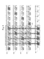
- FIGS. 5 and 6 illustrate an alternative embodiment of a low power and low cost stacked die solution that avoids offsetting adjacent die
- a plurality of semiconductor dies 502 a - 502 d are provided and stacked.
- Each die includes a formed TSV array 504 that corresponds to a pad array formed on each of the opposing die surfaces, with each via oriented orthogonally to the planar die surfaces and extending from one surface to the other.
- I/O circuitry 508 may be formed at each pad location 510 (phantom), but with circuitry 512 that enables selective coupling to a given via or pad.
- a programmable fuse or anti-fuse may be employed to electrically decouple the I/O circuitry from the I/O pad. In so doing, the capacitive loading that would normally take place with a coupled I/O circuit (even when disabled) is avoided.
- a group of vias in a given semiconductor device will electrically couple to I/O circuitry on that device, while at least a portion of the remaining vias will be electrically decoupled from I/O circuits disposed adjacent their respective via pads.
- FIG. 6 illustrates the assembled alignment of stacked semiconductor dies 602 a - 602 d with respect to a base semiconductor die 604 . While each I/O pad location includes I/O circuitry, for the first stacked device 602 a , respective fuses have decoupled the I/O circuitry at Locations 2, 3 and 4 from the respective I/O pads (represented by “open” connections between each pad and I/O circuitry, such as at 606 ). Similar de-fusings are carried out with the remaining stacked dies.
- employing programmable fuses enables a device manufacturer to avoid masking out selected I/O locations, although at a cost of creating the fuses.
- effecting point-to-point paths with the stacked die merely involves programming the fuses appropriately, such that a single via path coupling multiple devices couples to less than all of the I/O circuits adjacent that via path.
- the net result of using fuses allows the die stack to take on a true vertically aligned structure, with no offsets or process steps to precisely align offsets.
- FIG. 7 generally illustrates how a serial bus 700 may be used in a daisy-chained manner to initialize selected fuses 702 on each die 704 .
- Other ways to accomplish this include providing horizontal offset paths between adjacent devices to direct enable signals to the separate devices; enabling each device to measure a resistance of a given via path so that it can determine where it lies in the stack; or providing wirebond connections to drive device selection inputs.
- FIG. 8 illustrates one general topology for interconnecting master and slave dies in a memory system 800 .
- the system employs an integrated circuit (IC) memory controller 802 that interfaces with a plurality of IC memory devices 804 a - 804 d via point-to-point data buses 806 and a multi-drop address/control bus 808 .
- IC integrated circuit
- the point-to-point paths generally interconnect data I/O circuitry on the controller with corresponding data I/O circuitry on each memory device.
- the multi-drop address/control bus routes address and control signals from the memory controller to all of the devices.
- the memory devices 804 a - 804 d generally load the multi-drop bus in aggregate, while loading each point-to-point path individually.
- DRAM dynamic random access memory
- Non-volatile memory devices are also well suited to benefit from the unique die stacking arrangements disclosed herein.
- various other topologies are suitable for the embodiments described herein, such as where all of the interconnections comprise either point-to-point paths, or multi-drop paths.
- circuits disclosed herein may be described using computer aided design tools and expressed (or represented), as data and/or instructions embodied in various computer-readable media, in terms of their behavioral, register transfer, logic component, transistor, layout geometries, and/or other characteristics.
- Formats of files and other objects in which such circuit expressions may be implemented include, but are not limited to, formats supporting behavioral languages such as C, Verilog, and VHDL, formats supporting register level description languages like RTL, and formats supporting geometry description languages such as GDSII, GDSIII, GDSIV, CIF, MEBES and any other suitable formats and languages.
- Computer-readable media in which such formatted data and/or instructions may be embodied include, but are not limited to, non-volatile storage media in various forms (e.g., optical, magnetic or semiconductor storage media) and carrier waves that may be used to transfer such formatted data and/or instructions through wireless, optical, or wired signaling media or any combination thereof.
- Examples of transfers of such formatted data and/or instructions by carrier waves include, but are not limited to, transfers (uploads, downloads, e-mail, etc.) over the Internet and/or other computer networks via one or more data transfer protocols (e.g., HTTP, FTP, SMTP, etc.).
- Such data and/or instruction-based expressions of the above described circuits may be processed by a processing entity (e.g., one or more processors) within the computer system in conjunction with execution of one or more other computer programs including, without limitation, net-list generation programs, place and route programs and the like, to generate a representation or image of a physical manifestation of such circuits.
- a processing entity e.g., one or more processors
- Such representation or image may thereafter be used in device fabrication, for example, by enabling generation of one or more masks that are used to form various components of the circuits in a device fabrication process.
- signals described or depicted as having active-high or active-low logic levels may have opposite logic levels in alternative embodiments.
- Component circuitry within integrated circuit devices may be implemented using metal oxide semiconductor (MOS) technology, bipolar technology or any other technology in which logical and analog circuits may be implemented.
- MOS metal oxide semiconductor
- a signal is said to be “asserted” when the signal is driven to a low or high logic state (or charged to a high logic state or discharged to a low logic state) to indicate a particular condition.
- a signal is said to be “deasserted” to indicate that the signal is driven (or charged or discharged) to a state other than the asserted state (including a high or low logic state, or the floating state that may occur when the signal driving circuit is transitioned to a high impedance condition, such as an open drain or open collector condition).
- a signal driving circuit is said to “output” a signal to a signal receiving circuit when the signal driving circuit asserts (or deasserts, if explicitly stated or indicated by context) the signal on a signal line coupled between the signal driving and signal receiving circuits.
- a signal line is said to be “activated” when a signal is asserted on the signal line, and “deactivated” when the signal is deasserted.
- the prefix symbol “/” attached to signal names indicates that the signal is an active low signal (i.e., the asserted state is a logic low state).
- a line over a signal name e.g., ‘ ⁇ signal name> ’ is also used to indicate an active low signal.
- the term “coupled” is used herein to express a direct connection as well as a connection through one or more intervening circuits or structures.
- Integrated circuit device “programming” may include, for example and without limitation, loading a control value into a register or other storage circuit within the device in response to a host instruction and thus controlling an operational aspect of the device, establishing a device configuration or controlling an operational aspect of the device through a one-time programming operation (e.g., blowing fuses within a configuration circuit during device production), and/or connecting one or more selected pins or other contact structures of the device to reference voltage lines (also referred to as strapping) to establish a particular device configuration or operation aspect of the device.
- a one-time programming operation e.g., blowing fuses within a configuration circuit during device production
- reference voltage lines also referred to as strapping
Abstract
A stacked semiconductor device is disclosed that includes a plurality of semiconductor dies. Each die has oppositely disposed first and second surfaces, with pads formed on each of the surfaces. A plurality of through-vias connect respective pads on the first surface to respective pads on the second surface. The through-vias include a first group of through-vias coupled to respective I/O circuitry on the semiconductor die and a second group of through-vias not coupled to I/O circuitry on the semiconductor die. The plurality of semiconductor dies are stacked such that the first group of through-vias in a first one of the plurality of semiconductor dies are aligned with respective ones of at least a portion of the second group of through-vias in a second one of the plurality of semiconductor dies.
Description
This application is a Continuation of U.S. Ser. No. 14/858,888, filed Sep. 18, 2015, entitled “Stacked Semiconductor Device”, which is a Continuation of U.S. Ser. No. 13/502,093, filed Apr. 13, 2012, entitled “Stacked Semiconductor Device”, now U.S. Pat. No. 9,142,262, which claims priority under 35 U.S.C. § 120 to International Application No. PCT/US2010/050273, published as WO 2011/049710 A2 on Apr. 28, 2011, which claims priority from U.S. Provisional Application No. 61/254,519, filed Oct. 23, 2009 and entitled “Stacked Semiconductor Device”. Application Ser. Nos. 14/858,888, 13/502,093, International Application No. PCT/US2010/050273 and U.S. Provisional Application No. 61/254,519 are hereby incorporated by reference in their entirety. The disclosure herein relates to semiconductor devices and more particularly to stacking configurations and methods for semiconductor devices.
Semiconductor packaging often involves assembling and electrically interconnecting groups of semiconductor devices together in space-efficient, yet inexpensive ways. One packaging approach involves stacking devices to reduce the horizontal footprint of the assembled system. Conventional stacking schemes typically rely on signal redistribution layers and/or wire-bond resources to provide electrical access to and from each device. Moreover, conventional stacking arrangements often overlook power efficiency concerns.
While conventional stacking methods work well for their intended applications, the need exists for power and cost efficient stacked die arrangements and methods. Embodiments of packaged semiconductor systems and methods described herein satisfy these needs.
Embodiments of the disclosure are illustrated by way of example, and not by way of limitation, in the figures of the accompanying drawings and in which like reference numerals refer to similar elements and in which:
Embodiments of systems and methods are described herein where a plurality of semiconductor devices employing through-silicon-vias are stacked to allow access of at least one of the semiconductor devices by way of through-silicon-vias in at least one other of the semiconductor devices. The through-silicon-vias are designed and device-aligned to reduce input/output (I/O) loading along a given via path. By reducing I/O loading on via paths, the system enables optimal point-to-point connections between I/O circuitry in a base device, and I/O circuitry in one of the plurality of devices. This, in turn, improves system speed and power efficiency. In one embodiment, the through-silicon-vias in each of the plurality of semiconductor devices are arranged in an array. Each semiconductor device has two opposing surfaces and a corresponding pad array on each of the opposing surfaces. The reduced I/O loading is achieved by staggering I/O circuits among a pad array and offsetting adjacent devices by at least one pad location. In other words, the two adjacent devices are offset from each other by at least the distance between two adjacent columns of pads such that the first column of the through-silicon-via array in a first one of the adjacent devices are aligned with respective ones of the second column of the through-silicon-via array in the other one of the adjacent devices, the second column of the through-silicon-via array in the first one of the adjacent devices are aligned with respective ones of the third column of the through-silicon-via array in the other one of the adjacent devices, etc. The cooperation between the staggered I/O circuits and the offsetting between adjacent devices minimizes the number of I/O circuits coupled to each via path, resulting in reduced I/O loading thereof. Alternatively, the alignment is accomplished through a straight-up stack without offsetting. In such an embodiment, the I/O circuitry is not staggered, but rather selectively enabled to reduce the I/O loadings.
With continued reference to FIGS. 1-3 , a processor die 108 preferably forms the base of the stack 100, but may be remotely disposed therefrom as the application dictates. The processor device 108 accesses a die higher in the stack, such as die 102 c, by way of some of the through-vias in the same die and some of the through-vias in the dies lower in the stack, such as dies 102 a and 102 b, i.e., these vias form via paths for accessing the die 102 c. The processor device 108 optionally employs a via array (shown in phantom in FIG. 3 ) that may or may not correspond to the stacked die via arrays depending on whether the active circuitry on the processor device is facing the stack.
Further referring to FIG. 1 , and more specifically the magnified callout, each of the I/O pads 110 may take one of several forms. Generally, each pad represents the area occupied by the via structure (the via post diameter in addition to the surrounding metal pad) that couples to a corresponding via structure on an adjacent silicon die. In one embodiment, each I/O pads 112 electrically couples to transmit and/or receiver circuits such as a driver/receiver pair (or transceiver) 114, and possibly electro-static-discharge (ESD) circuitry (not shown) associated with the transmit and/or receive circuits, on the same die. An optional programmable mode register 116 provides a selectable enable/disable state for the driver/receiver circuitry. The capacitive coupling of this I/O circuit type may have the ability to load a via path with capacitance on the order of hundreds of femptofarads.
In an effort to minimize the effects of I/O pad capacitance on via paths, and referring still to FIG. 1 , the non-I/O pads 111 are employed. In one embodiment, the non-I/O pads are pads not having any associated I/O circuitry (e.g., driver/transceiver pair and ESD circuitry). In one embodiment, illustrated more clearly in FIG. 2 , only one in every four pad locations (such as at 210) in a given row of pads 212 (in phantom) is formed with I/O circuitry, defining a staggered I/O circuit pattern. This allows for point-to-point connections between processor die 208 and up to four semiconductor dies 202 a-202 d stacked above the processor die 208. For ease of reference in the discussion that follows, the shaded I/O pad location for an I/O pad on each stacked device of FIG. 2 will be referred to as “Location1”, with subsequent adjacent locations for non-I/O pads referred to in order as Locations 2 through 4.
In one embodiment, the point-to-point connectivity enables sizing of the I/O transceivers on the processor device for driving/receiving signals to/from one load (as opposed to multiple loads for a multi-drop configuration). The sizing may be in terms of current or voltage driving capability or the like. This, in turn, provides significant power savings, especially as the number of I/Os scale upwards for a given device stack.
With continued reference to FIG. 2 , from an overall stack perspective, representations of end-to-end vias from a cross-sectional view are shown as vertically interconnected paths 214, 216, 218, and 220. From an individual device perspective, the via array generally reflects the array shape, size, and pitch exhibited by the pad array.
Referring now to FIG. 3 , each TSV 300 is formed to provide a conductive path 302 oriented orthogonally between the active surface of the die 304 and the backside surface of the die 306. A raised pad structure 308 caps each via end. Pads disposed on the active surface of the die are generally formed coextensive with, and may actually define the I/O contact pads. Thus, for a given die, depending on the regular “stagger” of the I/O circuit pattern described above, a first set or group of vias will be coupled to I/O pads, while at least a portion of the rest (a second group) will be coupled to non-I/O pads on that die (no active circuitry). Note that the base die 310 in a given stack may optionally employ the via array 314 (in phantom) since its active circuitry lies on the top surface, at 312. In one embodiment, the plurality of semiconductor dies are stacked such that the first group of through-vias in a first one of the plurality of semiconductor dies (e.g., die 102 a) are aligned with respective ones of at least a portion of the second group of through-vias in a second one of the plurality of semiconductor dies (i.e., die 102 b).
Preferably, the semiconductor dies are identical in terms of structural form, but may differ somewhat in performance. Employing identical devices in the stack simplifies die stacking, alignment, and reduces the cost per unit through the benefits of volume manufacturing.
Referring back to FIGS. 1 and 2 , in one embodiment, the plurality of semiconductor dies are substantially identical and are offset from each other to achieve alignment of the first group of through-vias in a first one of the plurality of semiconductor dies with respective ones of at least a portion of the second group of through-vias in a second one of the plurality of semiconductor dies. For example, the stacked semiconductor dies can be aligned in such a way that the TSV arrays of adjacent dies are offset by at least one pad location. The die offsets create a “stairstep” arrangement for the stack, beginning at one edge of the pad array, and progressing by at least one pad location for each subsequently stacked device. The offsets allow the vias to electrically cooperate with the I/O circuit pattern formations on each die (preferably structurally identical). This is done such that each via path 214, 216, 218, and 220 (connected at one end to processor die I/ O circuits 222, 224, 226, and 228) couples to only one I/O circuit (“location 1”) in only one of the stacked dies.
With continued reference to FIG. 2 , the couplings from the base die I/ O circuits 222, 224, 226, and 228 to each stacked die “Location1” are illustrated at 210 a, 210 b, 210 c, and 210 d. For the specific instance where four dies are to be stacked, and one of every four pad locations (in a row of pads) for each die include I/O circuitry, a single pad offset in a staircase manner results in an alignment where groups of vias not coupled to I/O circuits on their own respective die ( pad locations 2, 3, and 4 for each set of four I/O locations) make electrical contact to I/O circuitry in different devices. Conversely, the alignment enables vias coupled to the I/O circuitry for pad Location 1 (for the lower-most stacked device 202 a) to interface with groups of vias not coupled to I/O circuitry ( pad locations 4, 3 and 2 of stacked devices 202 b, 202 c and 202 d, respectively). In this specific manner, each via path forms a true point-to-point connection between the processor I/O circuit and one I/O circuit formed in one of the stacked semiconductor devices.
In some instances, there may be a desire to add capacity and stack additional die over and above the originally designed stack. Each additional die will preferably be formed with the appropriate TSV array, but may lack the staggered I/O pad array described above to cooperate properly with the TSV aligned offset scheme. Instead, each I/O location on the additional device may employ conventional pad I/O circuitry, including a programmable register to enable the driver/receiver circuitry. For enabled I/O circuitry, the result on the corresponding electrically coupled end-to-end via path will be a multi-drop situation. For non-enabled I/O circuits on the additional device, a capacitive loading will exist on the corresponding via (even though the active circuitry is “off”). While the added device presents a slight overall capacitive load to each via, the overall power benefit achieved by the original stack more than makes up for the loading.
In some applications, both point-to-point and multi-drop paths may need to be realized in the stacked die. Multi-drop paths are often employed in memory systems to transfer common signals such as address, command and control signals from a memory controller to memory dies. This may be done in a variety of different ways. For example, a group of adjacent I/O circuits on the processor (for example, pad locations 1-4 of the processor die) may be tied or grouped together electrically to form a super-pad such that a commonly transmitted signal is transferred to the same I/O circuit location on all of the stacked die. Another approach involves populating a stretch of via sites with I/O circuitry similar to FIG. 6 , although modified such that four I/O sites are coupled from the processor 604 to sixteen I/O sites in semiconductor devices 602 a-602 d. Generally, the approach unscrambles the four received signals (along each row of four I/O sites) from the processor in each of the four semiconductor devices 602 a-602 d by rotating the four bits by 0, 1, 2, or 3 bit positions, depending on the device location in the stack.
Manufacturing the stacked semiconductor devices in accordance with the embodiment described above involves relatively straightforward fabrication methods including staggering the I/O pad pattern (with the I/O circuitry), fabricating the TSV array, and aligning the devices in a stacked relationship.
Formation of the I/O circuitry and pad array for each device may be accomplished during wafer fabrication, involving generally understood principles of integrated circuit device processing. Of interest is the notion that for each device, pad locations are preferably reserved for I/O circuitry, even if omitted. This runs counter to the trend of electrically utilizing every possible piece of silicon real estate. However, this cost is more than offset by the advantages in power savings that result. By designing the device such that the overall chip layout is identical among devices, fabrication costs due to stacked-die-specific applications may be spread out or amortized due to volume manufacturing.
Fabricating the TSV array for each device may occur at the wafer (device) level, or stacked die level. Referring again to FIG. 3 , the two stacked die 310 and 311 are illustrated that each exhibit a pair of TSVs 300. Openings 301 to initially define the via shapes may be formed at the device level through a plasma or chemical etching or mechanical drilling process. At the stacked level, the via arrays may be efficiently formed by a suitable drilling method where openings are formed through all of the stacked devices in a single drilling step. Following formation of the via openings, a suitable conductor such as aluminum is deposited therein to form an electrically conductive path 302. Each end of the via is capped off with a raised pad contact 308 suitable for engaging a confronting pad contact, such as that at 309 from an adjacent stacked die. Pads formed at the active surface 304 of the die 311 electrically couple to the pad I/O locations. If I/O circuitry for a given pad was masked during I/O fabrication, then the via will not be coupled to I/O circuitry.
Following formation of the TSV array for each die, singulated die are aligned to each other in a stacked relationship such that the TSV arrays for adjacent devices (corresponding to the pad arrays) are offset by at least one pad location. This is accomplished during assembly through well-known registration techniques, such as that shown in FIG. 4 , wherein each die 400 a-400 d includes a pair of identically located registration reticles 402 and 404. The reticles in-turn are aligned with a pair of die pads (not shown). By aligning the leftmost reticle 402 of one die to the rightmost reticle 404 of an adjacent die (note that the dies are generally thinned and transparent during processing to allow visual alignment), a die-to-die offset of one pad may be straightforwardly achieved.
As each die is stacked in offset relationship to the die beneath it, pads from the lower surface of the upper device engage aligned pads disposed on the upper surface of the lower device. Once the stack is completely assembled, electrically conductive paths will extend orthogonally from the lowest device (typically a processor chip) up through the entire stack of identically formed dies.
In operation, the via signal paths define channels that are susceptible to various loading effects. Specifically, capacitance associated with each via affects current usage and related power efficiency parameters. However, by employing point-to-point signaling paths with the via and I/O circuit arrangement described above, each end-to-end via path electrically couples to (preferably) one I/O circuit. With each I/O circuit having the potential to load a via by a few hundred femptofarads, eliminating capacitance associated with three out of every four potential pad locations significantly improves power efficiency.
Unlike the previously described embodiment, I/O circuitry 508 may be formed at each pad location 510 (phantom), but with circuitry 512 that enables selective coupling to a given via or pad. In one embodiment, a programmable fuse or anti-fuse may be employed to electrically decouple the I/O circuitry from the I/O pad. In so doing, the capacitive loading that would normally take place with a coupled I/O circuit (even when disabled) is avoided.
Thus, for each semiconductor device, a group of vias in a given semiconductor device will electrically couple to I/O circuitry on that device, while at least a portion of the remaining vias will be electrically decoupled from I/O circuits disposed adjacent their respective via pads.
Referring back to FIGS. 5 and 6 , employing programmable fuses enables a device manufacturer to avoid masking out selected I/O locations, although at a cost of creating the fuses. With all of the I/O pad locations exhibiting identical circuitry, effecting point-to-point paths with the stacked die merely involves programming the fuses appropriately, such that a single via path coupling multiple devices couples to less than all of the I/O circuits adjacent that via path. The net result of using fuses allows the die stack to take on a true vertically aligned structure, with no offsets or process steps to precisely align offsets.
One additional process step in assembling the stack in accordance with the fuse embodiment described above involves initializing the fuses to arrive at the desired coupled/decoupled structures. FIG. 7 generally illustrates how a serial bus 700 may be used in a daisy-chained manner to initialize selected fuses 702 on each die 704. Other ways to accomplish this include providing horizontal offset paths between adjacent devices to direct enable signals to the separate devices; enabling each device to measure a resistance of a given via path so that it can determine where it lies in the stack; or providing wirebond connections to drive device selection inputs.
In the embodiments described above, an emphasis on limiting the via to pad I/O electrical coupling to one circuit was applied. In practice, as long as at least one I/O circuit is decoupled from the via path, or less than all of the I/O circuits are coupled to the via path, power savings may be realized. Moreover, although point-to-point paths for the via connections were emphasized above, multi-drop connections that still provide power and cost savings may be beneficial.
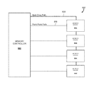
The stacked die structures described above are particularly well-suited for low-cost master-slave applications such as memory systems, where a master processing device, such as a memory controller, interfaces with a plurality of slave devices, such as memory devices. FIG. 8 illustrates one general topology for interconnecting master and slave dies in a memory system 800. The system employs an integrated circuit (IC) memory controller 802 that interfaces with a plurality of IC memory devices 804 a-804 d via point-to-point data buses 806 and a multi-drop address/control bus 808. The point-to-point paths generally interconnect data I/O circuitry on the controller with corresponding data I/O circuitry on each memory device. The multi-drop address/control bus routes address and control signals from the memory controller to all of the devices.
With continued reference to FIG. 8 , the memory devices 804 a-804 d generally load the multi-drop bus in aggregate, while loading each point-to-point path individually. Preferably, dynamic random access memory (DRAM) devices are employed in the die stack with a corresponding DRAM controller. Non-volatile memory devices are also well suited to benefit from the unique die stacking arrangements disclosed herein. In addition to the system topology shown in FIG. 8 , various other topologies are suitable for the embodiments described herein, such as where all of the interconnections comprise either point-to-point paths, or multi-drop paths.
It should be noted that the various circuits disclosed herein may be described using computer aided design tools and expressed (or represented), as data and/or instructions embodied in various computer-readable media, in terms of their behavioral, register transfer, logic component, transistor, layout geometries, and/or other characteristics. Formats of files and other objects in which such circuit expressions may be implemented include, but are not limited to, formats supporting behavioral languages such as C, Verilog, and VHDL, formats supporting register level description languages like RTL, and formats supporting geometry description languages such as GDSII, GDSIII, GDSIV, CIF, MEBES and any other suitable formats and languages. Computer-readable media in which such formatted data and/or instructions may be embodied include, but are not limited to, non-volatile storage media in various forms (e.g., optical, magnetic or semiconductor storage media) and carrier waves that may be used to transfer such formatted data and/or instructions through wireless, optical, or wired signaling media or any combination thereof. Examples of transfers of such formatted data and/or instructions by carrier waves include, but are not limited to, transfers (uploads, downloads, e-mail, etc.) over the Internet and/or other computer networks via one or more data transfer protocols (e.g., HTTP, FTP, SMTP, etc.).
When received within a computer system via one or more computer-readable media, such data and/or instruction-based expressions of the above described circuits may be processed by a processing entity (e.g., one or more processors) within the computer system in conjunction with execution of one or more other computer programs including, without limitation, net-list generation programs, place and route programs and the like, to generate a representation or image of a physical manifestation of such circuits. Such representation or image may thereafter be used in device fabrication, for example, by enabling generation of one or more masks that are used to form various components of the circuits in a device fabrication process.
In the foregoing description and in the accompanying drawings, specific terminology and drawing symbols have been set forth to provide a thorough understanding of the present invention. In some instances, the terminology and symbols may imply specific details that are not required to practice the invention. For example, any of the specific numbers of bits, signal path widths, signaling or operating frequencies, component circuits or devices and the like may be different from those described above in alternative embodiments. Also, the interconnection between circuit elements or circuit blocks shown or described as multi-conductor signal links may alternatively be single-conductor signal links, and single conductor signal links may alternatively be multi-conductor signal links. Signals and signaling paths shown or described as being single-ended may also be differential, and vice-versa. Similarly, signals described or depicted as having active-high or active-low logic levels may have opposite logic levels in alternative embodiments. Component circuitry within integrated circuit devices may be implemented using metal oxide semiconductor (MOS) technology, bipolar technology or any other technology in which logical and analog circuits may be implemented. With respect to terminology, a signal is said to be “asserted” when the signal is driven to a low or high logic state (or charged to a high logic state or discharged to a low logic state) to indicate a particular condition. Conversely, a signal is said to be “deasserted” to indicate that the signal is driven (or charged or discharged) to a state other than the asserted state (including a high or low logic state, or the floating state that may occur when the signal driving circuit is transitioned to a high impedance condition, such as an open drain or open collector condition). A signal driving circuit is said to “output” a signal to a signal receiving circuit when the signal driving circuit asserts (or deasserts, if explicitly stated or indicated by context) the signal on a signal line coupled between the signal driving and signal receiving circuits. A signal line is said to be “activated” when a signal is asserted on the signal line, and “deactivated” when the signal is deasserted. Additionally, the prefix symbol “/” attached to signal names indicates that the signal is an active low signal (i.e., the asserted state is a logic low state). A line over a signal name (e.g., ‘<signal name> ’) is also used to indicate an active low signal. The term “coupled” is used herein to express a direct connection as well as a connection through one or more intervening circuits or structures. Integrated circuit device “programming” may include, for example and without limitation, loading a control value into a register or other storage circuit within the device in response to a host instruction and thus controlling an operational aspect of the device, establishing a device configuration or controlling an operational aspect of the device through a one-time programming operation (e.g., blowing fuses within a configuration circuit during device production), and/or connecting one or more selected pins or other contact structures of the device to reference voltage lines (also referred to as strapping) to establish a particular device configuration or operation aspect of the device. The term “exemplary” is used to express an example, not a preference or requirement.
While the invention has been described with reference to specific embodiments thereof, it will be evident that various modifications and changes may be made thereto without departing from the broader spirit and scope of the invention. For example, features or aspects of any of the embodiments may be applied, at least where practicable, in combination with any other of the embodiments or in place of counterpart features or aspects thereof. Accordingly, the specification and drawings are to be regarded in an illustrative rather than a restrictive sense.
Claims (20)
1. A memory device for coupling with a logic integrated circuit (IC) chip having a first data input/output (I/O) circuit for transferring data signals, the memory device comprising:
a first memory IC chip having a second data I/O circuit formed at a first location on the first memory IC chip;
a second memory IC chip stacked with the first memory IC chip, the second memory IC chip including a third data I/O circuit formed at a second location on the second memory IC chip that corresponds to the first location on the first memory IC chip; and
a link selectively coupled to the second data I/O and the third I/O, the link for establishing a point-to-point data connection between the first data I/O circuit and one of the second data I/O circuit or the third data I/O circuit.
2. The memory device according to claim 1 , wherein the first and second memory IC chips comprise DRAM memory devices, and wherein the data signals represent information to be stored in one of the DRAM memory devices.
3. The memory according to claim 2 , wherein the logic IC chip comprises a DRAM memory controller.
4. The memory according to claim 1 , wherein the link comprises a through-silicon-via (TSV).
5. The memory according to claim 1 , wherein the second data I/O circuit of the first memory IC is vertically aligned with the third data I/O circuit of the second memory IC, and the link is for selectively connecting the first data I/O circuit to one of the third data I/O circuit and the second data I/O circuit.
6. The memory according to claim 5 , wherein the link connects to the third data I/O circuit via a programmable fuse.
7. The memory according to claim 1 , wherein the stacking of the first memory IC is laterally offset with respect to the second memory IC such that the third data I/O circuit is misaligned with the second data I/O circuit.
8. The memory device according to claim 1 , wherein each of the first and second memory IC chips further includes respective control/address I/O circuits, and wherein the memory device further comprises a multi-drop link coupled to the respective control/address I/O circuits.
9. The memory device according to claim 1 , wherein the first and second memory IC chips comprise non-volatile memory devices.
10. A memory comprising:
a logic integrated circuit (IC) chip having a first data input/output (I/O) circuit;
a first memory IC chip stacked with the logic IC chip and having a second data I/O circuit formed at a first location on the first memory IC chip;
a second memory IC chip stacked with the first memory IC chip, the second memory chip including a third data I/O circuit formed at a second location on the second memory IC chip that corresponds to the first location on the first memory IC chip; and
a point-to-point link selectively connecting the first data I/O circuit to the third data I/O circuit.
11. The memory according to claim 10 , wherein the first and second memory IC chips comprise DRAM memory devices.
12. The memory according to claim 10 , wherein the logic IC chip comprises a DRAM memory controller.
13. The memory according to claim 10 , wherein the point-to-point link comprises a through-silicon-via (TSV).
14. The memory according to claim 10 , wherein the second data I/O circuit of the first memory IC is vertically aligned with the third data I/O circuit of the second memory IC, and the point-to-point link selectively connects the first data I/O circuit to one of the third data I/O circuit and the second data I/O circuit.
15. The memory according to claim 14 , wherein the point-to-point link connects to the third data I/O circuit via a programmable fuse.
16. The memory according to claim 10 , wherein the stacking of the first memory IC is laterally offset with respect to the second memory IC such that the third data I/O circuit vertically aligns with the first data I/O circuit, and the second data I/O circuit is offset from the first data I/O circuit.
17. The memory according to claim 10 , wherein each of the logic and first and second memory IC chips further includes respective control/address I/O circuits, and wherein the memory further comprises a multi-drop link coupled to the respective control/address I/O circuits.
18. The memory according to claim 10 , wherein the first and second memory IC chips comprise non-volatile memory devices.
19. A method of operating a memory having a memory controller IC chip stacked with multiple memory device IC chips, the method comprising:
transferring data signals between the memory controller IC chip and each of the multiple memory device IC chips along through-silicon via point-to-point links, each of the through-silicon via point-to-point links being selectively connected between the memory controller IC chip and a separate one of the multiple memory device IC chips; and
transferring control/address (C/A) signals between the memory controller IC chip and each of the memory device IC chips along at least one through-silicon via multi-drop link.
20. The method according to claim 19 , wherein the transferring data signals and transferring C/A signals is carried out in accordance with a DRAM protocol.
Priority Applications (4)
Application Number | Priority Date | Filing Date | Title |
---|---|---|---|
US15/175,933 US9881663B2 (en) | 2009-10-23 | 2016-06-07 | Stacked semiconductor device |
US15/872,840 US10475505B2 (en) | 2009-10-23 | 2018-01-16 | Stacked semiconductor device |
US16/667,844 US11170842B2 (en) | 2009-10-23 | 2019-10-29 | Stacked semiconductor device |
US17/508,861 US11862235B2 (en) | 2009-10-23 | 2021-10-22 | Stacked semiconductor device |
Applications Claiming Priority (5)
Application Number | Priority Date | Filing Date | Title |
---|---|---|---|
US25451909P | 2009-10-23 | 2009-10-23 | |
PCT/US2010/050273 WO2011049710A2 (en) | 2009-10-23 | 2010-09-24 | Stacked semiconductor device |
US201213502093A | 2012-04-13 | 2012-04-13 | |
US14/858,888 US9362002B2 (en) | 2009-10-23 | 2015-09-18 | Stacked semiconductor device |
US15/175,933 US9881663B2 (en) | 2009-10-23 | 2016-06-07 | Stacked semiconductor device |
Related Parent Applications (1)
Application Number | Title | Priority Date | Filing Date |
---|---|---|---|
US14/858,888 Continuation US9362002B2 (en) | 2009-10-23 | 2015-09-18 | Stacked semiconductor device |
Related Child Applications (1)
Application Number | Title | Priority Date | Filing Date |
---|---|---|---|
US15/872,840 Continuation US10475505B2 (en) | 2009-10-23 | 2018-01-16 | Stacked semiconductor device |
Publications (2)
Publication Number | Publication Date |
---|---|
US20160365136A1 US20160365136A1 (en) | 2016-12-15 |
US9881663B2 true US9881663B2 (en) | 2018-01-30 |
Family
ID=43900884
Family Applications (6)
Application Number | Title | Priority Date | Filing Date |
---|---|---|---|
US13/502,093 Active 2032-10-21 US9142262B2 (en) | 2009-10-23 | 2010-09-24 | Stacked semiconductor device |
US14/858,888 Active US9362002B2 (en) | 2009-10-23 | 2015-09-18 | Stacked semiconductor device |
US15/175,933 Active US9881663B2 (en) | 2009-10-23 | 2016-06-07 | Stacked semiconductor device |
US15/872,840 Active US10475505B2 (en) | 2009-10-23 | 2018-01-16 | Stacked semiconductor device |
US16/667,844 Active US11170842B2 (en) | 2009-10-23 | 2019-10-29 | Stacked semiconductor device |
US17/508,861 Active US11862235B2 (en) | 2009-10-23 | 2021-10-22 | Stacked semiconductor device |
Family Applications Before (2)
Application Number | Title | Priority Date | Filing Date |
---|---|---|---|
US13/502,093 Active 2032-10-21 US9142262B2 (en) | 2009-10-23 | 2010-09-24 | Stacked semiconductor device |
US14/858,888 Active US9362002B2 (en) | 2009-10-23 | 2015-09-18 | Stacked semiconductor device |
Family Applications After (3)
Application Number | Title | Priority Date | Filing Date |
---|---|---|---|
US15/872,840 Active US10475505B2 (en) | 2009-10-23 | 2018-01-16 | Stacked semiconductor device |
US16/667,844 Active US11170842B2 (en) | 2009-10-23 | 2019-10-29 | Stacked semiconductor device |
US17/508,861 Active US11862235B2 (en) | 2009-10-23 | 2021-10-22 | Stacked semiconductor device |
Country Status (3)
Country | Link |
---|---|
US (6) | US9142262B2 (en) |
CN (1) | CN102598255A (en) |
WO (1) | WO2011049710A2 (en) |
Families Citing this family (40)
Publication number | Priority date | Publication date | Assignee | Title |
---|---|---|---|---|
US8787060B2 (en) | 2010-11-03 | 2014-07-22 | Netlist, Inc. | Method and apparatus for optimizing driver load in a memory package |
CN202758883U (en) | 2009-05-26 | 2013-02-27 | 拉姆伯斯公司 | Stacked semiconductor device assembly |
US9142262B2 (en) | 2009-10-23 | 2015-09-22 | Rambus Inc. | Stacked semiconductor device |
US8421237B2 (en) * | 2011-07-07 | 2013-04-16 | Cisco Technology, Inc. | Stacked memory layers having multiple orientations and through-layer interconnects |
WO2013033628A1 (en) | 2011-09-01 | 2013-03-07 | Rambus Inc. | Testing through-silicon-vias |
US8982598B2 (en) | 2012-04-18 | 2015-03-17 | Rambus Inc. | Stacked memory device with redundant resources to correct defects |
CN104854760A (en) | 2012-09-03 | 2015-08-19 | 艾布雷德斯公司 | Method for smart-contact arrays and stacked devices |
KR102017809B1 (en) * | 2013-02-27 | 2019-09-03 | 에스케이하이닉스 주식회사 | Chip die and semiconductor memory device including the same |
US9703321B2 (en) | 2013-07-09 | 2017-07-11 | I-Blades, Inc. | Snap on wearable module |
US10026666B2 (en) | 2013-10-18 | 2018-07-17 | Rambus Inc. | Stacked die package with aligned active and passive through-silicon vias |
US9658281B2 (en) * | 2013-10-25 | 2017-05-23 | Taiwan Semiconductor Manufacturing Company Limited | Alignment testing for tiered semiconductor structure |
IN2013CH05121A (en) * | 2013-11-12 | 2015-05-29 | Sandisk Technologies Inc | |
KR102301573B1 (en) | 2014-06-05 | 2021-09-10 | 삼성전자주식회사 | Semiconductor device |
US20160078939A1 (en) * | 2014-09-11 | 2016-03-17 | Intel Corporation | Appointing semiconductor dice to enable high stacking capability |
US9356001B2 (en) | 2014-10-02 | 2016-05-31 | HGST Netherlands B.V. | Semiconductor device with at least one voltage-guided conductive filament |
US10002653B2 (en) | 2014-10-28 | 2018-06-19 | Nxp Usa, Inc. | Die stack address bus having a programmable width |
KR20160068550A (en) * | 2014-12-05 | 2016-06-15 | 에스케이하이닉스 주식회사 | Semiconductor Apparatus Including Multi-chips Package |
KR20160069275A (en) * | 2014-12-08 | 2016-06-16 | 에스케이하이닉스 주식회사 | Semiconductor apparatus having electrical connections with through-via and metal layer and stacking method thereof |
KR102384724B1 (en) * | 2015-10-12 | 2022-04-12 | 에스케이하이닉스 주식회사 | Multi-chip package |
KR20170059616A (en) * | 2015-11-23 | 2017-05-31 | 에스케이하이닉스 주식회사 | Stacked memory device and semiconductor memory system |
US10133841B1 (en) * | 2016-09-30 | 2018-11-20 | Cadence Design Systems, Inc. | Methods, systems, and computer program product for implementing three-dimensional integrated circuit designs |
US10672743B2 (en) | 2016-10-07 | 2020-06-02 | Xcelsis Corporation | 3D Compute circuit with high density z-axis interconnects |
US10593667B2 (en) * | 2016-10-07 | 2020-03-17 | Xcelsis Corporation | 3D chip with shielded clock lines |
US10672663B2 (en) | 2016-10-07 | 2020-06-02 | Xcelsis Corporation | 3D chip sharing power circuit |
US10672744B2 (en) | 2016-10-07 | 2020-06-02 | Xcelsis Corporation | 3D compute circuit with high density Z-axis interconnects |
US10586786B2 (en) * | 2016-10-07 | 2020-03-10 | Xcelsis Corporation | 3D chip sharing clock interconnect layer |
US10600691B2 (en) | 2016-10-07 | 2020-03-24 | Xcelsis Corporation | 3D chip sharing power interconnect layer |
WO2018067719A2 (en) | 2016-10-07 | 2018-04-12 | Invensas Bonding Technologies, Inc. | Direct-bonded native interconnects and active base die |
US10600780B2 (en) * | 2016-10-07 | 2020-03-24 | Xcelsis Corporation | 3D chip sharing data bus circuit |
US10762420B2 (en) | 2017-08-03 | 2020-09-01 | Xcelsis Corporation | Self repairing neural network |
US10672745B2 (en) | 2016-10-07 | 2020-06-02 | Xcelsis Corporation | 3D processor |
US10600735B2 (en) * | 2016-10-07 | 2020-03-24 | Xcelsis Corporation | 3D chip sharing data bus |
US10580757B2 (en) * | 2016-10-07 | 2020-03-03 | Xcelsis Corporation | Face-to-face mounted IC dies with orthogonal top interconnect layers |
US10580735B2 (en) | 2016-10-07 | 2020-03-03 | Xcelsis Corporation | Stacked IC structure with system level wiring on multiple sides of the IC die |
US9966363B1 (en) * | 2017-02-03 | 2018-05-08 | Nanya Technology Corporation | Semiconductor apparatus and method for preparing the same |
WO2019079631A1 (en) * | 2017-10-20 | 2019-04-25 | Xcelsis Corporation | Face-to-face mounted ic dies with orthogonal top interconnect layers |
KR102450580B1 (en) | 2017-12-22 | 2022-10-07 | 삼성전자주식회사 | Semiconductor Device having a Structure for Insulating Layer under Metal Line |
EP3833007B1 (en) * | 2018-07-31 | 2024-03-13 | Sony Semiconductor Solutions Corporation | Layered-type light-receiving sensor and electronic device |
US11599299B2 (en) | 2019-11-19 | 2023-03-07 | Invensas Llc | 3D memory circuit |
US20210305159A1 (en) * | 2020-03-27 | 2021-09-30 | Micron Technology, Inc. | Microelectronic device interface configurations, and associated methods, devices, and systems |
Citations (39)
Publication number | Priority date | Publication date | Assignee | Title |
---|---|---|---|---|
US5585675A (en) | 1994-05-11 | 1996-12-17 | Harris Corporation | Semiconductor die packaging tub having angularly offset pad-to-pad via structure configured to allow three-dimensional stacking and electrical interconnections among multiple identical tubs |
US6177296B1 (en) | 1994-06-23 | 2001-01-23 | Cubic Memory Inc. | Method for forming vertical interconnect process for silicon segments with thermally conductive epoxy preform |
US6271587B1 (en) | 1999-09-15 | 2001-08-07 | Robert Patti | Connection arrangement for enbaling the use of identical chips in 3-dimensional stacks of chips requiring address specific to each chip |
US20010045645A1 (en) * | 2000-04-20 | 2001-11-29 | Kabushiki Kaisha Toshiba | Multichip semiconductor device and memory card |
US20030146012A1 (en) | 2002-02-06 | 2003-08-07 | Song Young Hee | Semiconductor chip, chip stack package and manufacturing method |
US6706546B2 (en) | 1998-10-09 | 2004-03-16 | Fujitsu Limited | Optical reflective structures and method for making |
US20040245615A1 (en) | 2003-06-03 | 2004-12-09 | Staktek Group, L.P. | Point to point memory expansion system and method |
US20050194674A1 (en) | 2004-03-02 | 2005-09-08 | Jochen Thomas | Integrated circuit with re-route layer and stacked die assembly |
US7071546B2 (en) | 2002-01-16 | 2006-07-04 | Alfred E. Mann Foundation For Scientific Research | Space-saving packaging of electronic circuits |
US7098541B2 (en) | 2003-05-19 | 2006-08-29 | Hewlett-Packard Development Company, L.P. | Interconnect method for directly connected stacked integrated circuits |
US20060205120A1 (en) | 2002-10-28 | 2006-09-14 | Eliyahou Harari | Flash Memory Cell Arrays Having Dual Control Gates Per Memory Cell Charge Storage Element |
US20070057384A1 (en) | 2005-09-14 | 2007-03-15 | Alam Syed M | Semiconductor stacked die/wafer configuration and packaging and method thereof |
US20070235851A1 (en) | 2006-04-11 | 2007-10-11 | Ware Frederick A | Point-to-point connection topology for stacked devices |
US20080031076A1 (en) * | 2006-07-26 | 2008-02-07 | International Business Machines Corporation | Daisy Chainable Memory Chip |
US20080088031A1 (en) | 2006-10-03 | 2008-04-17 | Samsung Electronics Co., Ltd. | Semiconductor package structure and method of fabricating the same |
US20080130395A1 (en) | 2005-08-30 | 2008-06-05 | Micron Technology, Inc. | Self-identifying stacked die semiconductor components |
US20080220565A1 (en) | 2007-03-09 | 2008-09-11 | Chao-Shun Hsu | Design techniques for stacking identical memory dies |
US7446420B1 (en) | 2007-06-20 | 2008-11-04 | Hynix Semiconductor Inc. | Through silicon via chip stack package capable of facilitating chip selection during device operation |
US20080315331A1 (en) | 2007-06-25 | 2008-12-25 | Robert Gideon Wodnicki | Ultrasound system with through via interconnect structure |
US20090039492A1 (en) | 2007-08-06 | 2009-02-12 | Samsung Electronics Co., Ltd. | Stacked memory device |
JP2009129498A (en) | 2007-11-22 | 2009-06-11 | Toshiba Corp | Semiconductor storage device |
US20090153177A1 (en) | 2007-12-07 | 2009-06-18 | Elpida Memory, Inc. | Separate testing of continuity between an internal terminal in each chip and an external terminal in a stacked semiconductor device |
US20090161401A1 (en) | 2007-12-24 | 2009-06-25 | Christoph Bilger | Multi-die Memory, Apparatus and Multi-die Memory Stack |
US20090161402A1 (en) | 2007-12-20 | 2009-06-25 | Hakjune Oh | Data storage and stackable configurations |
US20090180257A1 (en) | 2008-01-15 | 2009-07-16 | Samsung Electronics Co., Ltd. | Stacked semiconductor apparatus, system and method of fabrication |
US7816776B2 (en) | 2007-11-21 | 2010-10-19 | Samsung Electronics Co., Ltd. | Stacked semiconductor device and method of forming serial path thereof |
US20100289131A1 (en) | 2009-05-18 | 2010-11-18 | Stats Chippac, Ltd. | Semiconductor Device and Method of Forming Overlapping Semiconductor Die with Coplanar Vertical Interconnect Structure |
WO2010138480A2 (en) | 2009-05-26 | 2010-12-02 | Rambus Inc. | Stacked semiconductor device assembly |
US7898834B2 (en) | 2008-01-25 | 2011-03-01 | Hynix Semiconductor Inc. | Semiconductor chip with chip selection structure and stacked semiconductor package having the same |
US20110050320A1 (en) | 2009-09-02 | 2011-03-03 | Mosaid Technologies Incorporated | Using interrupted through-silicon-vias in integrated circuits adapted for stacking |
WO2011049710A2 (en) | 2009-10-23 | 2011-04-28 | Rambus Inc. | Stacked semiconductor device |
US20110148469A1 (en) * | 2009-12-18 | 2011-06-23 | Yutaka Ito | Stacked device detection and identification |
US8233303B2 (en) * | 2006-12-14 | 2012-07-31 | Rambus Inc. | Multi-die memory device |
US8258619B2 (en) | 2009-11-12 | 2012-09-04 | International Business Machines Corporation | Integrated circuit die stacks with translationally compatible vias |
WO2013025205A1 (en) | 2011-08-16 | 2013-02-21 | Intel Corporation | Offset interposers for large-bottom packages and large-die package-on-package structures |
US8432027B2 (en) | 2009-11-11 | 2013-04-30 | International Business Machines Corporation | Integrated circuit die stacks with rotationally symmetric vias |
US8436477B2 (en) | 2011-10-03 | 2013-05-07 | Invensas Corporation | Stub minimization using duplicate sets of signal terminals in assemblies without wirebonds to package substrate |
US8513817B2 (en) | 2011-07-12 | 2013-08-20 | Invensas Corporation | Memory module in a package |
US9432298B1 (en) * | 2011-12-09 | 2016-08-30 | P4tents1, LLC | System, method, and computer program product for improving memory systems |
Family Cites Families (9)
Publication number | Priority date | Publication date | Assignee | Title |
---|---|---|---|---|
JP4722305B2 (en) * | 2001-02-27 | 2011-07-13 | 富士通セミコンダクター株式会社 | Memory system |
US6417695B1 (en) * | 2001-03-15 | 2002-07-09 | Micron Technology, Inc. | Antifuse reroute of dies |
JP4423453B2 (en) * | 2005-05-25 | 2010-03-03 | エルピーダメモリ株式会社 | Semiconductor memory device |
US7609567B2 (en) * | 2005-06-24 | 2009-10-27 | Metaram, Inc. | System and method for simulating an aspect of a memory circuit |
US20070220207A1 (en) * | 2006-03-14 | 2007-09-20 | Bryan Black | Transferring data from stacked memory |
JP2008140220A (en) * | 2006-12-04 | 2008-06-19 | Nec Corp | Semiconductor device |
US7616509B2 (en) * | 2007-07-13 | 2009-11-10 | Freescale Semiconductor, Inc. | Dynamic voltage adjustment for memory |
US8031505B2 (en) * | 2008-07-25 | 2011-10-04 | Samsung Electronics Co., Ltd. | Stacked memory module and system |
KR102451650B1 (en) * | 2016-02-05 | 2022-10-11 | 에스케이하이닉스 주식회사 | Stacked type seniconductor apparatus |
-
2010
- 2010-09-24 US US13/502,093 patent/US9142262B2/en active Active
- 2010-09-24 WO PCT/US2010/050273 patent/WO2011049710A2/en active Application Filing
- 2010-09-24 CN CN201080047911XA patent/CN102598255A/en active Pending
-
2015
- 2015-09-18 US US14/858,888 patent/US9362002B2/en active Active
-
2016
- 2016-06-07 US US15/175,933 patent/US9881663B2/en active Active
-
2018
- 2018-01-16 US US15/872,840 patent/US10475505B2/en active Active
-
2019
- 2019-10-29 US US16/667,844 patent/US11170842B2/en active Active
-
2021
- 2021-10-22 US US17/508,861 patent/US11862235B2/en active Active
Patent Citations (41)
Publication number | Priority date | Publication date | Assignee | Title |
---|---|---|---|---|
US5585675A (en) | 1994-05-11 | 1996-12-17 | Harris Corporation | Semiconductor die packaging tub having angularly offset pad-to-pad via structure configured to allow three-dimensional stacking and electrical interconnections among multiple identical tubs |
US6177296B1 (en) | 1994-06-23 | 2001-01-23 | Cubic Memory Inc. | Method for forming vertical interconnect process for silicon segments with thermally conductive epoxy preform |
US6706546B2 (en) | 1998-10-09 | 2004-03-16 | Fujitsu Limited | Optical reflective structures and method for making |
US6271587B1 (en) | 1999-09-15 | 2001-08-07 | Robert Patti | Connection arrangement for enbaling the use of identical chips in 3-dimensional stacks of chips requiring address specific to each chip |
US20010045645A1 (en) * | 2000-04-20 | 2001-11-29 | Kabushiki Kaisha Toshiba | Multichip semiconductor device and memory card |
US7071546B2 (en) | 2002-01-16 | 2006-07-04 | Alfred E. Mann Foundation For Scientific Research | Space-saving packaging of electronic circuits |
US20030146012A1 (en) | 2002-02-06 | 2003-08-07 | Song Young Hee | Semiconductor chip, chip stack package and manufacturing method |
US7208343B2 (en) | 2002-02-06 | 2007-04-24 | Samsung Electronics Co., Ltd. | Semiconductor chip, chip stack package and manufacturing method |
US20060205120A1 (en) | 2002-10-28 | 2006-09-14 | Eliyahou Harari | Flash Memory Cell Arrays Having Dual Control Gates Per Memory Cell Charge Storage Element |
US7098541B2 (en) | 2003-05-19 | 2006-08-29 | Hewlett-Packard Development Company, L.P. | Interconnect method for directly connected stacked integrated circuits |
US20040245615A1 (en) | 2003-06-03 | 2004-12-09 | Staktek Group, L.P. | Point to point memory expansion system and method |
US20050194674A1 (en) | 2004-03-02 | 2005-09-08 | Jochen Thomas | Integrated circuit with re-route layer and stacked die assembly |
US20080130395A1 (en) | 2005-08-30 | 2008-06-05 | Micron Technology, Inc. | Self-identifying stacked die semiconductor components |
US20070057384A1 (en) | 2005-09-14 | 2007-03-15 | Alam Syed M | Semiconductor stacked die/wafer configuration and packaging and method thereof |
US20070235851A1 (en) | 2006-04-11 | 2007-10-11 | Ware Frederick A | Point-to-point connection topology for stacked devices |
US20080031076A1 (en) * | 2006-07-26 | 2008-02-07 | International Business Machines Corporation | Daisy Chainable Memory Chip |
US20080088031A1 (en) | 2006-10-03 | 2008-04-17 | Samsung Electronics Co., Ltd. | Semiconductor package structure and method of fabricating the same |
KR100832845B1 (en) | 2006-10-03 | 2008-05-28 | 삼성전자주식회사 | Semiconductor Package Structure And Method Of Fabricating The Same |
US8233303B2 (en) * | 2006-12-14 | 2012-07-31 | Rambus Inc. | Multi-die memory device |
US20080220565A1 (en) | 2007-03-09 | 2008-09-11 | Chao-Shun Hsu | Design techniques for stacking identical memory dies |
US7446420B1 (en) | 2007-06-20 | 2008-11-04 | Hynix Semiconductor Inc. | Through silicon via chip stack package capable of facilitating chip selection during device operation |
US20080315331A1 (en) | 2007-06-25 | 2008-12-25 | Robert Gideon Wodnicki | Ultrasound system with through via interconnect structure |
US20090039492A1 (en) | 2007-08-06 | 2009-02-12 | Samsung Electronics Co., Ltd. | Stacked memory device |
US7816776B2 (en) | 2007-11-21 | 2010-10-19 | Samsung Electronics Co., Ltd. | Stacked semiconductor device and method of forming serial path thereof |
JP2009129498A (en) | 2007-11-22 | 2009-06-11 | Toshiba Corp | Semiconductor storage device |
US20090153177A1 (en) | 2007-12-07 | 2009-06-18 | Elpida Memory, Inc. | Separate testing of continuity between an internal terminal in each chip and an external terminal in a stacked semiconductor device |
US20090161402A1 (en) | 2007-12-20 | 2009-06-25 | Hakjune Oh | Data storage and stackable configurations |
US20090161401A1 (en) | 2007-12-24 | 2009-06-25 | Christoph Bilger | Multi-die Memory, Apparatus and Multi-die Memory Stack |
US20090180257A1 (en) | 2008-01-15 | 2009-07-16 | Samsung Electronics Co., Ltd. | Stacked semiconductor apparatus, system and method of fabrication |
US7898834B2 (en) | 2008-01-25 | 2011-03-01 | Hynix Semiconductor Inc. | Semiconductor chip with chip selection structure and stacked semiconductor package having the same |
US20100289131A1 (en) | 2009-05-18 | 2010-11-18 | Stats Chippac, Ltd. | Semiconductor Device and Method of Forming Overlapping Semiconductor Die with Coplanar Vertical Interconnect Structure |
WO2010138480A2 (en) | 2009-05-26 | 2010-12-02 | Rambus Inc. | Stacked semiconductor device assembly |
US20110050320A1 (en) | 2009-09-02 | 2011-03-03 | Mosaid Technologies Incorporated | Using interrupted through-silicon-vias in integrated circuits adapted for stacking |
WO2011049710A2 (en) | 2009-10-23 | 2011-04-28 | Rambus Inc. | Stacked semiconductor device |
US8432027B2 (en) | 2009-11-11 | 2013-04-30 | International Business Machines Corporation | Integrated circuit die stacks with rotationally symmetric vias |
US8258619B2 (en) | 2009-11-12 | 2012-09-04 | International Business Machines Corporation | Integrated circuit die stacks with translationally compatible vias |
US20110148469A1 (en) * | 2009-12-18 | 2011-06-23 | Yutaka Ito | Stacked device detection and identification |
US8513817B2 (en) | 2011-07-12 | 2013-08-20 | Invensas Corporation | Memory module in a package |
WO2013025205A1 (en) | 2011-08-16 | 2013-02-21 | Intel Corporation | Offset interposers for large-bottom packages and large-die package-on-package structures |
US8436477B2 (en) | 2011-10-03 | 2013-05-07 | Invensas Corporation | Stub minimization using duplicate sets of signal terminals in assemblies without wirebonds to package substrate |
US9432298B1 (en) * | 2011-12-09 | 2016-08-30 | P4tents1, LLC | System, method, and computer program product for improving memory systems |
Non-Patent Citations (5)
Title |
---|
Amir, Duda et al., "3D Packaging, Interconnection & Assembly," 2013 Slidedeck downloaded from http://www.smta.org/chapters/files/Oregon-3D-Packaging-SMTA-CTP-2013-(Version-C).pdf. 196 pages. |
Amir, Duda et al., "3D Packaging, Interconnection & Assembly," 2013 Slidedeck downloaded from http://www.smta.org/chapters/files/Oregon—3D—Packaging—SMTA—CTP—2013—(Version—C).pdf. 196 pages. |
International Preliminary Report on Patentability dated May 3, 2012 re Int'l Application No. PCT/US10/050273. 5 pages. |
International Search Report and the written Opinion dated Jun. 9, 2011 re Int'l. Application No. PCT/US2010/050273. 8 Pages. |
Kang, Uksong et al., "8Gb 3D DDR3 DRAM Using Through-Silicon-Via Technology," IEEE International Solid-State Circuits Conference, 2009. 3 pages. |
Also Published As
Publication number | Publication date |
---|---|
US11862235B2 (en) | 2024-01-02 |
US10475505B2 (en) | 2019-11-12 |
CN102598255A (en) | 2012-07-18 |
US11170842B2 (en) | 2021-11-09 |
US9142262B2 (en) | 2015-09-22 |
US20200135262A1 (en) | 2020-04-30 |
WO2011049710A3 (en) | 2011-09-29 |
US20160365136A1 (en) | 2016-12-15 |
US20180211701A1 (en) | 2018-07-26 |
WO2011049710A2 (en) | 2011-04-28 |
US9362002B2 (en) | 2016-06-07 |
US20220139445A1 (en) | 2022-05-05 |
US20160012910A1 (en) | 2016-01-14 |
US20120201068A1 (en) | 2012-08-09 |
Similar Documents
Publication | Publication Date | Title |
---|---|---|
US11862235B2 (en) | Stacked semiconductor device | |
US11227639B2 (en) | Stacked DRAM device and method of manufacture | |
US7791175B2 (en) | Method for stacking serially-connected integrated circuits and multi-chip device made from same | |
TWI737832B (en) | Direct-bonded native interconnects and active base die | |
US9030004B2 (en) | Stacked semiconductor apparatus, system and method of fabrication | |
US9870982B2 (en) | Distributed on-chip decoupling apparatus and method using package interconnect | |
CN109599134B (en) | Flexible memory system with controller and memory stack | |
US10090236B2 (en) | Interposer having a pattern of sites for mounting chiplets | |
JP2012004559A (en) | Semiconductor chip package and method of manufacturing the same | |
CN102089826B (en) | Proximity optical memory module | |
CN113410223B (en) | Chip set and method for manufacturing the same | |
Clermidy et al. | 3D embedded multi-core: Some perspectives | |
CN113451260A (en) | Three-dimensional chip based on system bus and three-dimensional method thereof | |
TW202406088A (en) | Semiconductor devices and methods of manufacturing thereof | |
WO2012021310A1 (en) | Disaggregated semiconductor chip assembly and packaging technique |
Legal Events
Date | Code | Title | Description |
---|---|---|---|
AS | Assignment |
Owner name: RAMBUS INC., CALIFORNIA Free format text: ASSIGNMENT OF ASSIGNORS INTEREST;ASSIGNOR:WARE, FREDERICK A.;REEL/FRAME:038987/0605 Effective date: 20091208 |
|
STCF | Information on status: patent grant |
Free format text: PATENTED CASE |
|
MAFP | Maintenance fee payment |
Free format text: PAYMENT OF MAINTENANCE FEE, 4TH YEAR, LARGE ENTITY (ORIGINAL EVENT CODE: M1551); ENTITY STATUS OF PATENT OWNER: LARGE ENTITY Year of fee payment: 4 |