WO2020027230A1 - Layered type light-receiving sensor, and on-vehicle imaging device - Google Patents
Layered type light-receiving sensor, and on-vehicle imaging device Download PDFInfo
- Publication number
- WO2020027230A1 WO2020027230A1 PCT/JP2019/030093 JP2019030093W WO2020027230A1 WO 2020027230 A1 WO2020027230 A1 WO 2020027230A1 JP 2019030093 W JP2019030093 W JP 2019030093W WO 2020027230 A1 WO2020027230 A1 WO 2020027230A1
- Authority
- WO
- WIPO (PCT)
- Prior art keywords
- substrate
- vehicle
- imaging device
- unit
- image
- Prior art date
Links
- 238000003384 imaging method Methods 0.000 title claims description 180
- 239000000758 substrate Substances 0.000 claims abstract description 201
- 238000012545 processing Methods 0.000 claims abstract description 98
- 239000011159 matrix material Substances 0.000 claims abstract description 9
- 238000004364 calculation method Methods 0.000 claims description 19
- 230000010365 information processing Effects 0.000 claims description 7
- 238000013528 artificial neural network Methods 0.000 claims description 6
- 230000015654 memory Effects 0.000 description 58
- 238000010586 diagram Methods 0.000 description 45
- 238000000034 method Methods 0.000 description 38
- 238000005516 engineering process Methods 0.000 description 29
- 241000724291 Tobacco streak virus Species 0.000 description 22
- 238000001514 detection method Methods 0.000 description 22
- 230000001575 pathological effect Effects 0.000 description 22
- 238000004891 communication Methods 0.000 description 20
- 230000008569 process Effects 0.000 description 19
- 230000006870 function Effects 0.000 description 18
- 230000003287 optical effect Effects 0.000 description 18
- 210000001519 tissue Anatomy 0.000 description 14
- 230000000694 effects Effects 0.000 description 12
- 238000003745 diagnosis Methods 0.000 description 11
- 238000002674 endoscopic surgery Methods 0.000 description 11
- 235000019800 disodium phosphate Nutrition 0.000 description 9
- 230000005540 biological transmission Effects 0.000 description 7
- 239000011521 glass Substances 0.000 description 7
- 238000011144 upstream manufacturing Methods 0.000 description 7
- 238000012935 Averaging Methods 0.000 description 6
- 238000009795 derivation Methods 0.000 description 6
- 238000010801 machine learning Methods 0.000 description 6
- 238000010186 staining Methods 0.000 description 6
- 210000004027 cell Anatomy 0.000 description 5
- 230000007246 mechanism Effects 0.000 description 5
- 230000007170 pathology Effects 0.000 description 5
- 238000004458 analytical method Methods 0.000 description 4
- 230000008859 change Effects 0.000 description 4
- 239000003153 chemical reaction reagent Substances 0.000 description 4
- 230000006866 deterioration Effects 0.000 description 4
- 230000005284 excitation Effects 0.000 description 4
- 238000001356 surgical procedure Methods 0.000 description 4
- 238000003491 array Methods 0.000 description 3
- 238000004422 calculation algorithm Methods 0.000 description 3
- 239000010949 copper Substances 0.000 description 3
- 238000010336 energy treatment Methods 0.000 description 3
- 210000000056 organ Anatomy 0.000 description 3
- 238000010827 pathological analysis Methods 0.000 description 3
- 230000002194 synthesizing effect Effects 0.000 description 3
- XUIMIQQOPSSXEZ-UHFFFAOYSA-N Silicon Chemical compound [Si] XUIMIQQOPSSXEZ-UHFFFAOYSA-N 0.000 description 2
- 230000015572 biosynthetic process Effects 0.000 description 2
- 210000004204 blood vessel Anatomy 0.000 description 2
- 238000013461 design Methods 0.000 description 2
- 238000005401 electroluminescence Methods 0.000 description 2
- 238000003364 immunohistochemistry Methods 0.000 description 2
- MOFVSTNWEDAEEK-UHFFFAOYSA-M indocyanine green Chemical compound [Na+].[O-]S(=O)(=O)CCCCN1C2=CC=C3C=CC=CC3=C2C(C)(C)C1=CC=CC=CC=CC1=[N+](CCCCS([O-])(=O)=O)C2=CC=C(C=CC=C3)C3=C2C1(C)C MOFVSTNWEDAEEK-UHFFFAOYSA-M 0.000 description 2
- 229960004657 indocyanine green Drugs 0.000 description 2
- 238000009434 installation Methods 0.000 description 2
- 230000003902 lesion Effects 0.000 description 2
- 238000010295 mobile communication Methods 0.000 description 2
- 230000000149 penetrating effect Effects 0.000 description 2
- 230000009467 reduction Effects 0.000 description 2
- 239000004065 semiconductor Substances 0.000 description 2
- 229910052710 silicon Inorganic materials 0.000 description 2
- 239000010703 silicon Substances 0.000 description 2
- 238000003786 synthesis reaction Methods 0.000 description 2
- RYGMFSIKBFXOCR-UHFFFAOYSA-N Copper Chemical compound [Cu] RYGMFSIKBFXOCR-UHFFFAOYSA-N 0.000 description 1
- 241000252212 Danio rerio Species 0.000 description 1
- 206010028980 Neoplasm Diseases 0.000 description 1
- 230000001133 acceleration Effects 0.000 description 1
- 239000012620 biological material Substances 0.000 description 1
- 239000012472 biological sample Substances 0.000 description 1
- 230000000740 bleeding effect Effects 0.000 description 1
- 239000008280 blood Substances 0.000 description 1
- 210000004369 blood Anatomy 0.000 description 1
- 201000011510 cancer Diseases 0.000 description 1
- 238000006243 chemical reaction Methods 0.000 description 1
- 238000002485 combustion reaction Methods 0.000 description 1
- 239000002131 composite material Substances 0.000 description 1
- 239000000470 constituent Substances 0.000 description 1
- 229910052802 copper Inorganic materials 0.000 description 1
- 210000004748 cultured cell Anatomy 0.000 description 1
- 238000011161 development Methods 0.000 description 1
- 201000010099 disease Diseases 0.000 description 1
- 208000037265 diseases, disorders, signs and symptoms Diseases 0.000 description 1
- 239000000284 extract Substances 0.000 description 1
- 230000004438 eyesight Effects 0.000 description 1
- 238000002073 fluorescence micrograph Methods 0.000 description 1
- 230000004313 glare Effects 0.000 description 1
- 238000012744 immunostaining Methods 0.000 description 1
- 230000001678 irradiating effect Effects 0.000 description 1
- 230000031700 light absorption Effects 0.000 description 1
- 239000004973 liquid crystal related substance Substances 0.000 description 1
- 238000005259 measurement Methods 0.000 description 1
- 235000013372 meat Nutrition 0.000 description 1
- 239000003595 mist Substances 0.000 description 1
- 230000000116 mitigating effect Effects 0.000 description 1
- 238000012986 modification Methods 0.000 description 1
- 230000004048 modification Effects 0.000 description 1
- 210000004400 mucous membrane Anatomy 0.000 description 1
- 230000002107 myocardial effect Effects 0.000 description 1
- 238000003062 neural network model Methods 0.000 description 1
- 210000002569 neuron Anatomy 0.000 description 1
- 239000013307 optical fiber Substances 0.000 description 1
- 230000001151 other effect Effects 0.000 description 1
- 239000012188 paraffin wax Substances 0.000 description 1
- 230000002093 peripheral effect Effects 0.000 description 1
- 238000007781 pre-processing Methods 0.000 description 1
- 239000000955 prescription drug Substances 0.000 description 1
- 238000007639 printing Methods 0.000 description 1
- 230000006798 recombination Effects 0.000 description 1
- 238000005215 recombination Methods 0.000 description 1
- 238000011160 research Methods 0.000 description 1
- 230000004044 response Effects 0.000 description 1
- 210000003296 saliva Anatomy 0.000 description 1
- 238000007789 sealing Methods 0.000 description 1
- 230000035939 shock Effects 0.000 description 1
- 229910000679 solder Inorganic materials 0.000 description 1
- 239000007787 solid Substances 0.000 description 1
- 230000005236 sound signal Effects 0.000 description 1
- 230000002123 temporal effect Effects 0.000 description 1
- 230000000007 visual effect Effects 0.000 description 1
Images


Classifications
-
- H—ELECTRICITY
- H01—ELECTRIC ELEMENTS
- H01L—SEMICONDUCTOR DEVICES NOT COVERED BY CLASS H10
- H01L27/00—Devices consisting of a plurality of semiconductor or other solid-state components formed in or on a common substrate
- H01L27/14—Devices consisting of a plurality of semiconductor or other solid-state components formed in or on a common substrate including semiconductor components sensitive to infrared radiation, light, electromagnetic radiation of shorter wavelength or corpuscular radiation and specially adapted either for the conversion of the energy of such radiation into electrical energy or for the control of electrical energy by such radiation
- H01L27/144—Devices controlled by radiation
- H01L27/146—Imager structures
- H01L27/14601—Structural or functional details thereof
- H01L27/14634—Assemblies, i.e. Hybrid structures
-
- G—PHYSICS
- G06—COMPUTING; CALCULATING OR COUNTING
- G06F—ELECTRIC DIGITAL DATA PROCESSING
- G06F18/00—Pattern recognition
- G06F18/20—Analysing
- G06F18/21—Design or setup of recognition systems or techniques; Extraction of features in feature space; Blind source separation
- G06F18/214—Generating training patterns; Bootstrap methods, e.g. bagging or boosting
-
- G—PHYSICS
- G06—COMPUTING; CALCULATING OR COUNTING
- G06N—COMPUTING ARRANGEMENTS BASED ON SPECIFIC COMPUTATIONAL MODELS
- G06N3/00—Computing arrangements based on biological models
- G06N3/02—Neural networks
- G06N3/04—Architecture, e.g. interconnection topology
-
- G—PHYSICS
- G06—COMPUTING; CALCULATING OR COUNTING
- G06V—IMAGE OR VIDEO RECOGNITION OR UNDERSTANDING
- G06V10/00—Arrangements for image or video recognition or understanding
- G06V10/10—Image acquisition
- G06V10/12—Details of acquisition arrangements; Constructional details thereof
- G06V10/14—Optical characteristics of the device performing the acquisition or on the illumination arrangements
- G06V10/147—Details of sensors, e.g. sensor lenses
-
- G—PHYSICS
- G06—COMPUTING; CALCULATING OR COUNTING
- G06V—IMAGE OR VIDEO RECOGNITION OR UNDERSTANDING
- G06V10/00—Arrangements for image or video recognition or understanding
- G06V10/70—Arrangements for image or video recognition or understanding using pattern recognition or machine learning
- G06V10/764—Arrangements for image or video recognition or understanding using pattern recognition or machine learning using classification, e.g. of video objects
-
- G—PHYSICS
- G06—COMPUTING; CALCULATING OR COUNTING
- G06V—IMAGE OR VIDEO RECOGNITION OR UNDERSTANDING
- G06V10/00—Arrangements for image or video recognition or understanding
- G06V10/70—Arrangements for image or video recognition or understanding using pattern recognition or machine learning
- G06V10/82—Arrangements for image or video recognition or understanding using pattern recognition or machine learning using neural networks
-
- G—PHYSICS
- G06—COMPUTING; CALCULATING OR COUNTING
- G06V—IMAGE OR VIDEO RECOGNITION OR UNDERSTANDING
- G06V20/00—Scenes; Scene-specific elements
- G06V20/50—Context or environment of the image
- G06V20/56—Context or environment of the image exterior to a vehicle by using sensors mounted on the vehicle
- G06V20/58—Recognition of moving objects or obstacles, e.g. vehicles or pedestrians; Recognition of traffic objects, e.g. traffic signs, traffic lights or roads
- G06V20/584—Recognition of moving objects or obstacles, e.g. vehicles or pedestrians; Recognition of traffic objects, e.g. traffic signs, traffic lights or roads of vehicle lights or traffic lights
-
- G—PHYSICS
- G06—COMPUTING; CALCULATING OR COUNTING
- G06V—IMAGE OR VIDEO RECOGNITION OR UNDERSTANDING
- G06V20/00—Scenes; Scene-specific elements
- G06V20/50—Context or environment of the image
- G06V20/59—Context or environment of the image inside of a vehicle, e.g. relating to seat occupancy, driver state or inner lighting conditions
- G06V20/597—Recognising the driver's state or behaviour, e.g. attention or drowsiness
-
- H—ELECTRICITY
- H01—ELECTRIC ELEMENTS
- H01L—SEMICONDUCTOR DEVICES NOT COVERED BY CLASS H10
- H01L27/00—Devices consisting of a plurality of semiconductor or other solid-state components formed in or on a common substrate
- H01L27/14—Devices consisting of a plurality of semiconductor or other solid-state components formed in or on a common substrate including semiconductor components sensitive to infrared radiation, light, electromagnetic radiation of shorter wavelength or corpuscular radiation and specially adapted either for the conversion of the energy of such radiation into electrical energy or for the control of electrical energy by such radiation
- H01L27/144—Devices controlled by radiation
- H01L27/146—Imager structures
- H01L27/14601—Structural or functional details thereof
- H01L27/14636—Interconnect structures
-
- H—ELECTRICITY
- H04—ELECTRIC COMMUNICATION TECHNIQUE
- H04N—PICTORIAL COMMUNICATION, e.g. TELEVISION
- H04N23/00—Cameras or camera modules comprising electronic image sensors; Control thereof
- H04N23/60—Control of cameras or camera modules
- H04N23/617—Upgrading or updating of programs or applications for camera control
-
- H—ELECTRICITY
- H04—ELECTRIC COMMUNICATION TECHNIQUE
- H04N—PICTORIAL COMMUNICATION, e.g. TELEVISION
- H04N25/00—Circuitry of solid-state image sensors [SSIS]; Control thereof
- H04N25/40—Extracting pixel data from image sensors by controlling scanning circuits, e.g. by modifying the number of pixels sampled or to be sampled
- H04N25/44—Extracting pixel data from image sensors by controlling scanning circuits, e.g. by modifying the number of pixels sampled or to be sampled by partially reading an SSIS array
-
- H—ELECTRICITY
- H04—ELECTRIC COMMUNICATION TECHNIQUE
- H04N—PICTORIAL COMMUNICATION, e.g. TELEVISION
- H04N25/00—Circuitry of solid-state image sensors [SSIS]; Control thereof
- H04N25/70—SSIS architectures; Circuits associated therewith
- H04N25/709—Circuitry for control of the power supply
-
- H—ELECTRICITY
- H04—ELECTRIC COMMUNICATION TECHNIQUE
- H04N—PICTORIAL COMMUNICATION, e.g. TELEVISION
- H04N25/00—Circuitry of solid-state image sensors [SSIS]; Control thereof
- H04N25/70—SSIS architectures; Circuits associated therewith
- H04N25/71—Charge-coupled device [CCD] sensors; Charge-transfer registers specially adapted for CCD sensors
- H04N25/75—Circuitry for providing, modifying or processing image signals from the pixel array
-
- H—ELECTRICITY
- H04—ELECTRIC COMMUNICATION TECHNIQUE
- H04N—PICTORIAL COMMUNICATION, e.g. TELEVISION
- H04N25/00—Circuitry of solid-state image sensors [SSIS]; Control thereof
- H04N25/70—SSIS architectures; Circuits associated therewith
- H04N25/79—Arrangements of circuitry being divided between different or multiple substrates, chips or circuit boards, e.g. stacked image sensors
-
- H—ELECTRICITY
- H04—ELECTRIC COMMUNICATION TECHNIQUE
- H04N—PICTORIAL COMMUNICATION, e.g. TELEVISION
- H04N7/00—Television systems
- H04N7/18—Closed-circuit television [CCTV] systems, i.e. systems in which the video signal is not broadcast
Definitions
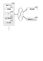
- FIG. 5 is a diagram showing a layout example of the second substrate according to the second layout example.
- the DSP 14 is arranged at the center of the area where the DSP 14 and the memory 15 are arranged.
- the memory 15 is arranged so as to surround the DSP 14 from four directions.
- the layout example of the first substrate 100 may be the same as the layout example described with reference to FIG. 3 in the first layout example.
- FIG. 6 is a diagram showing a layout example of the second substrate according to the third layout example.
- the DSP 14 is arranged adjacent to the signal processing unit 13 in the same layout as the first layout example. According to such a configuration, the signal line from the signal processing unit 13 to the DSP 14 can be shortened. This makes it possible to reduce signal delay, reduce signal and power supply voltage propagation loss, improve S / N ratio, and reduce power consumption.
- FIG. 24 is a block diagram showing an example of a functional configuration of the camera head 11102 and the CCU 11201 shown in FIG.
- imaging conditions such as the frame rate, the exposure value, the magnification, and the focus may be appropriately designated by the user, or may be automatically set by the control unit 11413 of the CCU 11201 based on the acquired image signal. Good.
- a so-called AE (Auto Exposure) function, an AF (Auto Focus) function, and an AWB (Auto White Balance) function are mounted on the endoscope 11100.
- the resolution of the tile image of the upper layer is ⁇ times the resolution of the tile image of the lower layer used for the synthesis. It has become.
- the configuration described above can be applied not only to the diagnosis support system but also to all biological microscopes such as a confocal microscope, a fluorescence microscope, and a video microscope.
- the observation target may be a biological sample such as a cultured cell, a fertilized egg, or a sperm, a biological material such as a cell sheet or a three-dimensional cell tissue, or a living body such as a zebrafish or a mouse.
- the observation target object is not limited to a glass slide, and can be observed in a state stored in a well plate, a petri dish, or the like.
Abstract
The present invention performs more advanced processing inside a chip. This layered type light-receiving sensor according to an embodiment comprises: a first substrate (100, 200, 300); a second substrate (120, 320) bonded to the first substrate; and connection wiring (402) attached to the second substrate. The first substrate includes a pixel array section (101) in which a plurality of unit pixels are arrayed in a two-dimensional matrix pattern. The second substrate includes: a converter (17A) for converting analog pixel signals output from the pixel array section into digital image data; and a processing unit (14) for processing data based on the image data. At least a portion of the converter is disposed on a first side of the second substrate, and the processing unit is disposed on a second side of the second substrate opposite to the first side. The connection wiring is attached to any side except the second side of the second substrate.
Description
本開示は、積層型受光センサ及び車載撮像装置に関する。
The present disclosure relates to a stacked light receiving sensor and an in-vehicle imaging device.
従来、静止画や動画を取得する撮像装置として、センサチップや、メモリチップや、DSP(Digital Signal Processor)チップなどのチップ同士を複数のバンプで並列に接続した平置き型のイメージセンサが存在する。
2. Description of the Related Art Conventionally, as an imaging apparatus for acquiring a still image or a moving image, there is a flat-type image sensor in which chips such as a sensor chip, a memory chip, and a DSP (Digital Signal Processor) chip are connected in parallel by a plurality of bumps. .
また、近年では、撮像装置の小型化を目的として、複数のダイが積層された積層構造を有する1チップのイメージセンサが提案されている。
In recent years, a one-chip image sensor having a stacked structure in which a plurality of dies are stacked has been proposed in order to reduce the size of an imaging device.
ところで、近年では、画像処理の多様化・高速化や個人情報の保護等の観点から、イメージセンサチップ内でより高度な処理を実行することが望まれている。
By the way, in recent years, from the viewpoints of diversification and speeding up of image processing, protection of personal information, and the like, it is desired to execute more advanced processing in the image sensor chip.
そこで本開示では、チップ内でより高度な処理を実行することが可能な積層型受光センサ及び車載撮像装置を提案する。
Therefore, the present disclosure proposes a stacked light-receiving sensor and an in-vehicle imaging device that can execute more advanced processing in a chip.
上記の課題を解決するために、本開示に係る一形態の積層型受光センサは、第1基板と、前記第1基板に貼り合わされた第2基板と、前記第2基板に取り付けられた接続配線とを備え、前記第1基板は、複数の単位画素が2次元マトリクス状に配列された画素アレイ部を備え、前記第2基板は、前記画素アレイ部から出力されるアナログの画素信号をデジタルの画像データへ変換する変換器と、前記画像データに基づくデータに対して処理を実行する処理部とを備え、前記変換器の少なくとも一部は、前記第2基板における第1辺側に配置され、前記処理部は、前記第2基板における前記第1辺とは反対の第2辺側に配置され、前記接続配線は、前記第2基板における前記第2辺以外の辺に取り付けられる。
In order to solve the above-described problems, a stacked light-receiving sensor according to one embodiment of the present disclosure includes a first substrate, a second substrate attached to the first substrate, and a connection wiring attached to the second substrate. Wherein the first substrate includes a pixel array unit in which a plurality of unit pixels are arranged in a two-dimensional matrix, and the second substrate converts an analog pixel signal output from the pixel array unit into a digital signal. A converter for converting to image data, and a processing unit that performs processing on data based on the image data, at least a portion of the converter is disposed on a first side of the second substrate, The processing unit is disposed on a second side of the second substrate opposite to the first side, and the connection wiring is attached to a side of the second substrate other than the second side.
以下に、本開示の一実施形態について図面に基づいて詳細に説明する。なお、以下の実施形態において、同一の部位には同一の符号を付することにより重複する説明を省略する。
Hereinafter, an embodiment of the present disclosure will be described in detail with reference to the drawings. In the following embodiments, the same portions are denoted by the same reference numerals, and redundant description will be omitted.
また、以下に示す項目順序に従って本開示を説明する。
1.第1の実施形態
1.1 撮像装置の概略構成例
1.2 イメージセンサチップのチップ構成例
1.3 学習済みモデルに基づく演算を実行する処理部を搭載したイメージセンサチップの課題
1.4 ノイズ低減手法
1.4.1 第1のレイアウト例
1.4.1.1 第1基板のレイアウト例
1.4.1.2 第2基板のレイアウト例
1.4.2 第2のレイアウト例
1.4.3 第3のレイアウト例
1.4.4 第4のレイアウト例
1.4.5 第5のレイアウト例
1.4.6 第6のレイアウト例
1.4.7 第7のレイアウト例
1.4.8 第8のレイアウト例
1.4.9 第9のレイアウト例
1.5 作用・効果
2.第2の実施形態
2.1 イメージセンサチップのチップ構成例
2.2 作用・効果
3.第3の実施形態
3.1 イメージセンサチップのチップ構成例
3.2 作用・効果
4.第4の実施形態
4.1 構成例
4.2 取り付け例
4.2.1 第1例
4.2.2 第2例
4.3 作用・効果
5.他のセンサへの適用
6.移動体への応用例
7.内視鏡手術システムへの応用例
8.WSI(Whole Slide Imaging)システムへの応用例 In addition, the present disclosure will be described according to the following item order.
1. 1. First Embodiment 1.1 Schematic Configuration Example of Imaging Device 1.2 Chip Configuration Example of Image Sensor Chip 1.3 Problems of Image Sensor Chip Mounted with Processing Unit for Performing Calculation Based on Learned Model 1.4 Noise Reduction method 1.4.1 First layout example 1.4.1.1 First board layout example 1.4.1.2 Second board layout example 1.4.2 Second layout example 4.3 Third Layout Example 1.4.4 Fourth Layout Example 1.4.5 Fifth Layout Example 1.4.6 Sixth Layout Example 1.4.7 Seventh Layout Example 4.8 Eighth layout example 1.4.9 Ninth layout example 1.5 Function and effect 2. Second Embodiment 2.1 Chip Configuration Example of Image Sensor Chip 2.2 Functions and Effects 3. Third embodiment 3.1 Example of chip configuration of image sensor chip 3.2 Functions and effects 4. Fourth embodiment 4.1 Configuration example 4.2 Mounting example 4.2.1 First example 4.2.2 Second example 4.3 Function / effect 5. 5. Application to other sensors 6. Application example to mobile object 7. Example of application to endoscopic surgery system Application example to WSI (Whole Slide Imaging) system
1.第1の実施形態
まず、第1の実施形態について、図面を参照して詳細に説明する。 1. First Embodiment First, a first embodiment will be described in detail with reference to the drawings.
まず、第1の実施形態について、図面を参照して詳細に説明する。 1. First Embodiment First, a first embodiment will be described in detail with reference to the drawings.
1.1 撮像装置の概略構成例
図1は、第1の実施形態に係る電子機器としての撮像装置の概略構成例を示すブロック図である。図1に示すように、撮像装置1は、固体撮像装置であるイメージセンサ10と、アプリケーションプロセッサ20とを備える。イメージセンサ10は、撮像部11と、コントロール部12と、変換器(Analog to Digital Converter:以下、ADCという)17と、信号処理部13と、DSP(Digital Signal Processor)14と、メモリ15と、セレクタ(出力部ともいう)16とを備えている。 1.1 Schematic Configuration Example of Imaging Apparatus FIG. 1 is a block diagram illustrating a schematic configuration example of an imaging apparatus as an electronic apparatus according to the first embodiment. As illustrated in FIG. 1, theimaging device 1 includes an image sensor 10 that is a solid-state imaging device, and an application processor 20. The image sensor 10 includes an imaging unit 11, a control unit 12, a converter (hereinafter, referred to as an ADC) 17, a signal processing unit 13, a DSP (Digital Signal Processor) 14, a memory 15, And a selector (also referred to as an output unit) 16.
図1は、第1の実施形態に係る電子機器としての撮像装置の概略構成例を示すブロック図である。図1に示すように、撮像装置1は、固体撮像装置であるイメージセンサ10と、アプリケーションプロセッサ20とを備える。イメージセンサ10は、撮像部11と、コントロール部12と、変換器(Analog to Digital Converter:以下、ADCという)17と、信号処理部13と、DSP(Digital Signal Processor)14と、メモリ15と、セレクタ(出力部ともいう)16とを備えている。 1.1 Schematic Configuration Example of Imaging Apparatus FIG. 1 is a block diagram illustrating a schematic configuration example of an imaging apparatus as an electronic apparatus according to the first embodiment. As illustrated in FIG. 1, the
コントロール部12は、例えば、ユーザの操作や設定された動作モードに従い、イメージセンサ10内の各部を制御する。
The control unit 12 controls each unit in the image sensor 10 according to, for example, a user operation or a set operation mode.
撮像部11は、例えば、ズームレンズ、フォーカスレンズ、絞り等を備える光学系104と、フォトダイオードなどの受光素子を含む単位画素(図2の単位画素101a)が2次元マトリクス状に配列した構成を備える画素アレイ部101とを備える。外部から入射した光は、光学系104を介することで、画素アレイ部101における受光素子が配列した受光面に結像される。画素アレイ部101の各単位画素101aは、その受光素子に入射した光を光電変換することで、入射光の光量に応じた電荷を読出可能に蓄積する。
The imaging unit 11 has, for example, a configuration in which an optical system 104 including a zoom lens, a focus lens, an aperture, and the like, and unit pixels (unit pixels 101a in FIG. 2) including light receiving elements such as photodiodes are arranged in a two-dimensional matrix. And a pixel array unit 101 provided. Light incident from the outside passes through the optical system 104 to form an image on a light receiving surface of the pixel array unit 101 on which light receiving elements are arranged. Each unit pixel 101a of the pixel array unit 101 photoelectrically converts light incident on the light receiving element, and accumulates a charge corresponding to the amount of incident light in a readable manner.
ADC17は、撮像部11から読み出された単位画素101a毎のアナログの画素信号をデジタル値に変換することで、デジタルの画像データを生成し、生成した画像データを信号処理部13及び/又はメモリ15へ出力する。なお、ADC17には、電源電圧等から撮像部11を駆動するための駆動電圧を生成する電圧生成回路等が含まれてもよい。
The ADC 17 generates digital image data by converting an analog pixel signal of each unit pixel 101a read from the imaging unit 11 into a digital value, and generates the generated image data by the signal processing unit 13 and / or the memory. 15 is output. The ADC 17 may include a voltage generation circuit that generates a drive voltage for driving the imaging unit 11 from a power supply voltage or the like.
信号処理部13は、ADC17から入力されたデジタルの画像データ又はメモリ15から読み出されたデジタルの画像データ(以下、処理対象の画像データという)に対して種々の信号処理を実行する。例えば、処理対象の画像データがカラー画像である場合、信号処理部13は、この画像データをYUVの画像データやRGBの画像データなどにフォーマット変換する。また、信号処理部13は、例えば、処理対象の画像データに対し、ノイズ除去やホワイトバランス調整等の処理を必要に応じて実行する。その他、信号処理部13は、処理対象の画像データに対し、DSP14がその画像データを処理するのに必要となる種々の信号処理(前処理ともいう)を実行する。
The signal processing unit 13 performs various signal processing on digital image data input from the ADC 17 or digital image data read from the memory 15 (hereinafter, referred to as processing target image data). For example, when the image data to be processed is a color image, the signal processing unit 13 converts the format of the image data into YUV image data, RGB image data, or the like. In addition, the signal processing unit 13 performs, for example, processing such as noise removal and white balance adjustment on the image data to be processed as necessary. In addition, the signal processing unit 13 performs various signal processing (also referred to as pre-processing) necessary for the DSP 14 to process the image data to be processed.
DSP14は、例えば、メモリ15に格納されているプログラムを実行することで、ディープニューラルネットワーク(DNN)を利用した機械学習によって作成された学習済みモデル(ニューラルネットワーク計算モデルともいう)を用いて各種処理を実行する処理部として機能する。この学習済みモデル(ニューラルネットワーク計算モデル)は、画素アレイ部101の出力に相当する入力信号と、当該入力信号に対するラベルとが紐付いている学習データとを所定の機械学習モデルに入力して生成されたパラメータに基づいて設計されていてもよい。また、所定の機械学習モデルは、多層のニューラルネットワークを利用した学習モデル(多層ニューラルネットワークモデルともいう)であってもよい。
The DSP 14 executes, for example, a program stored in the memory 15 to perform various processes using a learned model (also called a neural network calculation model) created by machine learning using a deep neural network (DNN). Function as a processing unit that executes This learned model (neural network calculation model) is generated by inputting an input signal corresponding to the output of the pixel array unit 101 and learning data associated with a label for the input signal to a predetermined machine learning model. It may be designed on the basis of the set parameters. The predetermined machine learning model may be a learning model using a multilayer neural network (also referred to as a multilayer neural network model).
例えば、DSP14は、メモリ15に記憶されている学習済みモデルに基づいた演算処理を実行することで、メモリ15に記憶されている辞書係数と画像データと掛け合わせる処理を実行する。このような演算処理により得られた結果(演算結果)は、メモリ15及び/又はセレクタ16へ出力される。なお、演算結果には、学習済みモデルを用いた演算処理を実行することで得られた画像データや、その画像データから得られる各種情報(メタデータ)が含まれ得る。また、DSP14には、メモリ15へのアクセスを制御するメモリコントローラが組み込まれていてもよい。
{For example, the DSP 14 executes a calculation process based on the learned model stored in the memory 15 to execute a process of multiplying the dictionary coefficient stored in the memory 15 by the image data. The result (calculation result) obtained by such calculation processing is output to the memory 15 and / or the selector 16. The calculation result may include image data obtained by executing a calculation process using the learned model, and various information (metadata) obtained from the image data. Further, the DSP 14 may include a memory controller for controlling access to the memory 15.
なお、DSP14が処理対象とする画像データは、画素アレイ部101から通常に読み出された画像データであってもよいし、この通常に読み出された画像データの画素を間引くことでデータサイズが縮小された画像データであってもよい。若しくは、画素アレイ部101に対して画素を間引いた読み出しを実行することで通常よりも小さいデータサイズで読み出された画像データであってもよい。なお、ここでの通常の読み出しとは、画素を間引かずに読み出すことであってよい。
Note that the image data to be processed by the DSP 14 may be image data normally read from the pixel array unit 101, or the data size may be reduced by thinning out pixels of the normally read image data. The image data may be reduced image data. Alternatively, the image data may be image data read out with a smaller data size than usual by executing reading out of the pixel array unit 101 by thinning out pixels. Note that the normal reading here may be reading without skipping pixels.
メモリ15は、ADC17から出力された画像データ、信号処理部13で信号処理された画像データ、DSP14で得られた演算結果等を必要に応じて記憶する。また、メモリ15は、DSP14が実行する学習済みモデルのアルゴリズムをプログラム及び辞書係数として記憶する。
The memory 15 stores the image data output from the ADC 17, the image data signal-processed by the signal processing unit 13, the calculation result obtained by the DSP 14, and the like as necessary. The memory 15 stores the algorithm of the learned model executed by the DSP 14 as a program and dictionary coefficients.
なお、DSP14は、学習データを用いて学習モデル内の各種パラメータの重み付けを変更することで学習モデルを学習したり、複数の学習モデルを用意しておき演算処理の内容に応じて使用する学習モデルを変更したり、外部の装置から学習済みの学習モデルを取得したりして、上記演算処理を実行することができる。
Note that the DSP 14 learns a learning model by changing the weights of various parameters in the learning model using the learning data, or prepares a plurality of learning models and uses the learning model according to the content of the arithmetic processing. , Or by acquiring a learned learning model from an external device to execute the arithmetic processing.
セレクタ16は、例えばコントロール部12からの選択制御信号に従うことで、DSP14から出力された画像データやメモリ15に記憶されている画像データや演算結果を選択的に出力する。なお、DSP14が信号処理部13から出力された画像データに対して処理を実行しない場合であって、セレクタ16がDSP14から出力された画像データを出力する場合には、セレクタ16は、信号処理部13から出力された画像データをそのまま出力する。
The selector 16 selectively outputs the image data output from the DSP 14, the image data stored in the memory 15, and the calculation result, for example, in accordance with a selection control signal from the control unit 12. Note that when the DSP 14 does not perform processing on the image data output from the signal processing unit 13 and the selector 16 outputs the image data output from the DSP 14, the selector 16 13 is output as it is.
以上のようにしてセレクタ16から出力された画像データや演算結果は、表示やユーザインタフェースなどを処理するアプリケーションプロセッサ20に入力される。アプリケーションプロセッサ20は、例えば、CPU(Central Processing Unit)等を用いて構成され、オペレーティングシステムや各種アプリケーションソフトウエア等を実行する。このアプリケーションプロセッサ20には、GPU(Graphics Processing Unit)やベースバンドプロセッサなどの機能が搭載されていてもよい。アプリケーションプロセッサ20は、入力された画像データや演算結果に対し、必要に応じた種々処理を実行したり、ユーザへの表示を実行したり、所定のネットワーク40を介して外部のクラウドサーバ30へ送信したりする。
The image data and the calculation result output from the selector 16 as described above are input to the application processor 20 that processes display and a user interface. The application processor 20 is configured using, for example, a CPU (Central Processing Unit) and executes an operating system and various application software. The application processor 20 may have functions such as a GPU (Graphics Processing Unit) and a baseband processor. The application processor 20 performs various processes as needed on the input image data and the calculation results, executes display to the user, and transmits the image data and the calculation result to the external cloud server 30 via the predetermined network 40. Or
なお、所定のネットワーク40には、例えば、インターネットや、有線LAN(Local Area Network)又は無線LANや、移動体通信網や、Bluetooth(登録商標)など、種々のネットワークを適用することができる。また、画像データや演算結果の送信先は、クラウドサーバ30に限定されず、単一で動作するサーバや、各種データを保管するファイルサーバや、携帯電話機等の通信端末など、通信機能を有する種々の情報処理装置(システム)であってよい。
Various networks such as the Internet, a wired LAN (Local Area Network) or a wireless LAN, a mobile communication network, and Bluetooth (registered trademark) can be applied to the predetermined network 40. In addition, the transmission destination of the image data and the calculation result is not limited to the cloud server 30, and various servers having a communication function such as a server that operates alone, a file server that stores various data, and a communication terminal such as a mobile phone. Information processing device (system).
1.2 イメージセンサチップのチップ構成例
次に、図1に示すイメージセンサ10のチップ構成の例について、以下に図面を参照して詳細に説明する。 1.2 Example of Chip Configuration of Image Sensor Chip Next, an example of a chip configuration of theimage sensor 10 illustrated in FIG. 1 will be described in detail below with reference to the drawings.
次に、図1に示すイメージセンサ10のチップ構成の例について、以下に図面を参照して詳細に説明する。 1.2 Example of Chip Configuration of Image Sensor Chip Next, an example of a chip configuration of the
図2は、本実施形態に係るイメージセンサのチップ構成例を示す模式図である。図2に示すように、イメージセンサ10は、四角形の平板状の第1基板(ダイ)100と、同じく四角形の平板状の第2基板(ダイ)120とが貼り合わされた積層構造を有している。
FIG. 2 is a schematic diagram illustrating an example of a chip configuration of the image sensor according to the present embodiment. As shown in FIG. 2, the image sensor 10 has a laminated structure in which a rectangular flat first substrate (die) 100 and a rectangular flat second substrate (die) 120 are bonded together. I have.
第1基板100と第2基板とのサイズは、例えば、同じであってよい。また、第1基板100と第2基板120とは、それぞれシリコン基板などの半導体基板であってよい。
サ イ ズ The size of the first substrate 100 and the size of the second substrate may be the same, for example. Further, the first substrate 100 and the second substrate 120 may be semiconductor substrates such as a silicon substrate.
第1基板100には、図1に示すイメージセンサ10の構成において、撮像部11の画素アレイ部101が配置される。また、第1基板100には、光学系104の一部又は全部がオンチップで設けられていてもよい。
(1) On the first substrate 100, the pixel array unit 101 of the imaging unit 11 in the configuration of the image sensor 10 shown in FIG. Further, a part or all of the optical system 104 may be provided on the first substrate 100 on a chip.
第2基板120には、図1に示すイメージセンサ10の構成において、ADC17と、コントロール部12と、信号処理部13と、DSP14と、メモリ15と、セレクタ16とが配置されている。なお、第2基板120には、不図示のインタフェース回路やドライバ回路などが配置されていてもよい。
1. On the second substrate 120, in the configuration of the image sensor 10 shown in FIG. 1, the ADC 17, the control unit 12, the signal processing unit 13, the DSP 14, the memory 15, and the selector 16 are arranged. Note that an interface circuit, a driver circuit, and the like (not shown) may be arranged on the second substrate 120.
第1基板100と第2基板120との貼り合わせは、第1基板100及び第2基板120をそれぞれチップに個片化した後、これら個片化された第1基板100及び第2基板120を貼り合わせる、いわゆるCoC(Chip on Chip)方式であってもよいし、第1基板100と第2基板120とのうち一方(例えば、第1基板100)をチップに個片化した後、この個片化された第1基板100を個片化前(すなわち、ウエハ状態)の第2基板120に貼り合わせる、いわゆるCoW(Chip on Wafer)方式であってもよいし、第1基板100と第2基板120とを共にウエハの状態で貼り合わせる、いわゆるWoW(Wafer on Wafer)方式であってもよい。
The bonding of the first substrate 100 and the second substrate 120 is performed by dividing the first substrate 100 and the second substrate 120 into chips, respectively, and then dividing the first substrate 100 and the second substrate 120 into individual chips. A so-called CoC (Chip-on-Chip) method of bonding may be used. Alternatively, one of the first substrate 100 and the second substrate 120 (for example, the first substrate 100) may be separated into chips, and then this chip may be separated. The so-called CoW (Chip on Wafer) method, in which the singulated first substrate 100 is bonded to the second substrate 120 before singulation (that is, in a wafer state), or the first substrate 100 and the second substrate 120 may be used. A so-called WoW (Wafer-on-Wafer) method may be used in which the substrate 120 and the substrate 120 are bonded together in a wafer state.
第1基板100と第2基板120との接合方法には、例えば、プラズマ接合等を使用することができる。ただし、これに限定されず、種々の接合方法が用いられてよい。
に は As a method for bonding the first substrate 100 and the second substrate 120, for example, plasma bonding or the like can be used. However, the present invention is not limited to this, and various joining methods may be used.
1.3 学習済みモデルに基づく演算を実行する処理部を搭載したイメージセンサチップの課題
以上のように、DSP14を学習済みモデルに基づいた演算処理を実行する処理部として動作させる場合、その動作アルゴリズムの実装が、プログラムの実行による、いわゆるソフトウエア実装となる。また、学習済みモデルの動作アルゴリズムは、日々更新されている。そのため、学習済みモデルに基づいた演算処理を実行するDSP14がどのタイミングで処理を実行するかや、DSP14の処理のピークがどのタイミングになるかなどを事前に把握することは困難である。 1.3 Problems of Image Sensor Chip Equipped with Processing Unit that Performs Calculation Based on Learned Model As described above, whenDSP 14 is operated as a processing unit that performs calculation processing based on a trained model, its operation algorithm Is a so-called software implementation by executing a program. The operation algorithm of the trained model is updated daily. For this reason, it is difficult to know in advance which timing the DSP 14 executing the arithmetic processing based on the learned model executes the processing, and which timing the peak of the processing of the DSP 14 will be.
以上のように、DSP14を学習済みモデルに基づいた演算処理を実行する処理部として動作させる場合、その動作アルゴリズムの実装が、プログラムの実行による、いわゆるソフトウエア実装となる。また、学習済みモデルの動作アルゴリズムは、日々更新されている。そのため、学習済みモデルに基づいた演算処理を実行するDSP14がどのタイミングで処理を実行するかや、DSP14の処理のピークがどのタイミングになるかなどを事前に把握することは困難である。 1.3 Problems of Image Sensor Chip Equipped with Processing Unit that Performs Calculation Based on Learned Model As described above, when
そして、図2に例示するように、第1基板100に画素アレイ部101を搭載し、第2基板120にDSP14を搭載したチップ構成において、DSP14を学習済みモデルに基づいた演算を実行する処理部として動作させる場合、画素アレイ部101のリセット中や画素アレイ部101の露光中や画素アレイ部101の各単位画素101aからの画素信号を読出中にDSP14が演算処理を開始したりDSP14の処理がピークを迎えたりすると、画素アレイ部101から読み出される画素信号にノイズが重畳され、結果的に、イメージセンサ10で取得する画像の品質が低下してしまう。
Then, as illustrated in FIG. 2, in a chip configuration in which the pixel array unit 101 is mounted on the first substrate 100 and the DSP 14 is mounted on the second substrate 120, the processing unit that executes an operation based on the learned model of the DSP 14 When the operation is performed as described above, the DSP 14 starts the arithmetic processing or the processing of the DSP 14 while the pixel array unit 101 is being reset, the pixel array unit 101 is being exposed, or the pixel signal from each unit pixel 101a of the pixel array unit 101 is being read. When the peak is reached, noise is superimposed on the pixel signal read from the pixel array unit 101, and as a result, the quality of the image acquired by the image sensor 10 deteriorates.
そこで本実施形態では、画素アレイ部101とDSP14との位置関係を調整することで、画素アレイ部101へのDSP14の信号処理に起因したノイズの入り込みを低減する。これにより、DSP14を学習済みモデルに基づいた演算を実行する処理部として動作させた場合でも、品質の劣化が低減された画像を取得することが可能となる。
Therefore, in the present embodiment, by adjusting the positional relationship between the pixel array unit 101 and the DSP 14, noise entering the pixel array unit 101 due to the signal processing of the DSP 14 is reduced. Accordingly, even when the DSP 14 is operated as a processing unit that executes an operation based on the learned model, it is possible to obtain an image with reduced quality deterioration.
1.4 ノイズ低減手法
次に、本実施形態に係る画素アレイ部101とDSP14との位置関係について、以下に図面を参照して詳細に説明する。なお、以下では、各層(第1基板100及び第2基板120)のレイアウト(フロアマップともいう)について幾つか例を挙げることで、画素アレイ部101とDSP14との位置関係を説明する。 1.4 Noise Reduction Method Next, the positional relationship between thepixel array unit 101 and the DSP 14 according to the present embodiment will be described in detail below with reference to the drawings. Hereinafter, the positional relationship between the pixel array unit 101 and the DSP 14 will be described by giving some examples of the layout (also referred to as a floor map) of each layer (the first substrate 100 and the second substrate 120).
次に、本実施形態に係る画素アレイ部101とDSP14との位置関係について、以下に図面を参照して詳細に説明する。なお、以下では、各層(第1基板100及び第2基板120)のレイアウト(フロアマップともいう)について幾つか例を挙げることで、画素アレイ部101とDSP14との位置関係を説明する。 1.4 Noise Reduction Method Next, the positional relationship between the
1.4.1 第1のレイアウト例
図3及び図4は、本実施形態に係る第1のレイアウト例を説明するための図である。なお、図3は、第1基板100のレイアウト例を示し、図4は、第2基板120のレイアウト例を示す。 1.4.1 First Layout Example FIGS. 3 and 4 are diagrams for explaining a first layout example according to the present embodiment. FIG. 3 shows a layout example of thefirst substrate 100, and FIG. 4 shows a layout example of the second substrate 120.
図3及び図4は、本実施形態に係る第1のレイアウト例を説明するための図である。なお、図3は、第1基板100のレイアウト例を示し、図4は、第2基板120のレイアウト例を示す。 1.4.1 First Layout Example FIGS. 3 and 4 are diagrams for explaining a first layout example according to the present embodiment. FIG. 3 shows a layout example of the
1.4.1.1 第1基板のレイアウト例
図3に示すように、第1基板100には、図1に示すイメージセンサ10の構成において、撮像部11の画素アレイ部101が配置されている。なお、第1基板100に光学系104の一部又は全部を搭載する場合には、画素アレイ部101と対応する位置に設けられる。 1.4.1.1 Example of Layout of First Substrate As shown in FIG. 3, thepixel array unit 101 of the imaging unit 11 in the configuration of the image sensor 10 shown in FIG. I have. When a part or all of the optical system 104 is mounted on the first substrate 100, the optical system 104 is provided at a position corresponding to the pixel array unit 101.
図3に示すように、第1基板100には、図1に示すイメージセンサ10の構成において、撮像部11の画素アレイ部101が配置されている。なお、第1基板100に光学系104の一部又は全部を搭載する場合には、画素アレイ部101と対応する位置に設けられる。 1.4.1.1 Example of Layout of First Substrate As shown in FIG. 3, the
画素アレイ部101は、第1基板100の4つの辺L101~L104のうち、1つの辺L101側に片寄って配置される。言い換えれば、画素アレイ部101は、その中心部O101が第1基板100の中心部O100よりも辺L101に近接するように、配置されている。なお、第1基板100における画素アレイ部101が設けられた面が長方形である場合、辺L101は、例えば、短い方の辺であってもよい。ただし、これに限定されず、長い方の辺に、画素アレイ部101が片寄って配置されてもよい。
The pixel array unit 101 is arranged to be shifted toward one side L101 among the four sides L101 to L104 of the first substrate 100. In other words, the pixel array unit 101 is arranged such that the center O101 is closer to the side L101 than the center O100 of the first substrate 100. When the surface of the first substrate 100 on which the pixel array unit 101 is provided is rectangular, the side L101 may be, for example, the shorter side. However, the present invention is not limited to this, and the pixel array unit 101 may be arranged to be offset on the longer side.
画素アレイ部101の4つの辺のうちの辺L101に近接する領域、言い換えれば、辺L101と画素アレイ部101との間の領域には、画素アレイ部101中の各単位画素101aを第2基板120に配置されたADC17に電気的に接続させるための配線として、第1基板100を貫通する複数の貫通配線(Through Silicon Via:以下、TSVという)が配列するTSVアレイ102が設けられている。このように、TSVアレイ102を画素アレイ部101が近接する辺L101に近接させることで、第2基板120において、ADC17等の各部を配置スペースを確保し易くすることができる。
Each of the unit pixels 101a in the pixel array unit 101 is placed in a region near the side L101 of the four sides of the pixel array unit 101, in other words, in a region between the side L101 and the pixel array unit 101. A TSV array 102 in which a plurality of through wirings (Through Silicon Via) (hereinafter, referred to as TSVs) penetrating the first substrate 100 is provided as wiring for electrically connecting to the ADC 17 arranged in the 120. As described above, by bringing the TSV array 102 close to the side L101 to which the pixel array unit 101 is close, it is possible to easily secure an arrangement space for each unit such as the ADC 17 on the second substrate 120.
なお、TSVアレイ102は、辺L101と交わる2つの辺L103及びL104のうち一方の辺L104(ただし、辺L103であってもよい)に近接する領域、言い換えれば、辺L104(又は、辺L103)と画素アレイ部101との間の領域にも設けられていてよい。
Note that the TSV array 102 has a region in the vicinity of one of the two sides L103 and L104 intersecting the side L101 (but may be the side L103), in other words, the side L104 (or the side L103). May be provided also in a region between the pixel array unit 101 and the pixel array unit 101.
第1基板100の4つの辺L101~L104のうち、画素アレイ部101が片寄って配置されていない辺L102~L103それぞれには、直線状に配列された複数のパッドよりなるパッドアレイ103が設けられている。パッドアレイ103に含まれるパッドには、例えば、画素アレイ部101やADC17などのアナログ回路用の電源電圧が印加されるパッド(電源ピンともいう)や、信号処理部13やDSP14やメモリ15やセレクタ16やコントロール部12等のデジタル回路用の電源電圧が印加されるパッド(電源ピンともいう)や、MIPI(Mobile Industry Processor Interface)やSPI(Serial Peripheral Interface)などのインタフェース用のパッド(信号ピンともいう)や、クロックやデータの入出力のためのパッド(信号ピンともいう)などが含まれている。各パッドは、例えば、外部の電源回路やインタフェース回路とワイヤを介して電気的に接続される。各パッドアレイ103とTSVアレイ102とは、パッドアレイ103中の各パッドに接続されたワイヤからの信号の反射の影響を無視できる程度に十分に離れていることが好ましい。
Of the four sides L101 to L104 of the first substrate 100, each of the sides L102 to L103 in which the pixel array unit 101 is not offset is provided with a pad array 103 including a plurality of pads arranged linearly. ing. The pads included in the pad array 103 include, for example, a pad (also referred to as a power supply pin) to which a power supply voltage for an analog circuit such as the pixel array unit 101 and the ADC 17 is applied, a signal processing unit 13, a DSP 14, a memory 15, and a selector. 16 and a pad (also referred to as a power supply pin) to which a power supply voltage for digital circuits such as the control unit 12 is applied, and an interface pad (also referred to as a signal pin) such as MIPI (Mobile Industry Processor Interface) or SPI (Serial Peripheral Interface). ), And pads (also called signal pins) for inputting and outputting clocks and data. Each pad is electrically connected to an external power supply circuit or interface circuit via a wire, for example. It is preferable that each pad array 103 and the TSV array 102 are sufficiently separated from each other in the pad array 103 so that the influence of signal reflection from a wire connected to each pad in the pad array 103 can be ignored.
1.4.1.2 第2基板のレイアウト例
一方、図4に示すように、第2基板120には、図1に示すイメージセンサ10の構成において、ADC17と、コントロール部12と、信号処理部13と、DSP14と、メモリ15とが配置されている。なお、第1のレイアウト例では、メモリ15がメモリ15Aとメモリ15Bとの2つの領域に分かれている。同様に、ADC17がADC17AとDAC(Digital to Analog Converter)17Bとの2つの領域に分かれている。DAC17Bは、ADC17AへAD変換用の参照電圧を供給する構成であり、広い意味でADC17の一部に含まれる構成である。また、図4には図示されていないが、セレクタ16も第2基板120に配置されている。 1.4.1.2 Example of Layout of Second Substrate On the other hand, as shown in FIG. 4, on thesecond substrate 120, in the configuration of the image sensor 10 shown in FIG. The section 13, the DSP 14, and the memory 15 are arranged. In the first layout example, the memory 15 is divided into two areas, a memory 15A and a memory 15B. Similarly, the ADC 17 is divided into two areas, an ADC 17A and a DAC (Digital to Analog Converter) 17B. The DAC 17B supplies a reference voltage for AD conversion to the ADC 17A, and is included in a part of the ADC 17 in a broad sense. Although not shown in FIG. 4, the selector 16 is also disposed on the second substrate 120.
一方、図4に示すように、第2基板120には、図1に示すイメージセンサ10の構成において、ADC17と、コントロール部12と、信号処理部13と、DSP14と、メモリ15とが配置されている。なお、第1のレイアウト例では、メモリ15がメモリ15Aとメモリ15Bとの2つの領域に分かれている。同様に、ADC17がADC17AとDAC(Digital to Analog Converter)17Bとの2つの領域に分かれている。DAC17Bは、ADC17AへAD変換用の参照電圧を供給する構成であり、広い意味でADC17の一部に含まれる構成である。また、図4には図示されていないが、セレクタ16も第2基板120に配置されている。 1.4.1.2 Example of Layout of Second Substrate On the other hand, as shown in FIG. 4, on the
さらに、第2基板120には、第1基板100を貫通するTSVアレイ102中の各TSV(以下、単にTSVアレイ102とする)と接触することで電気的に接続された配線122と、第1基板100のパッドアレイ103における各パッドと電気的に接続される複数のパッドが直線状に配列されてなるパッドアレイ123とが設けられている。
Further, the second substrate 120 includes a wiring 122 electrically connected to each TSV (hereinafter, simply referred to as the TSV array 102) in the TSV array 102 penetrating the first substrate 100, A pad array 123 in which a plurality of pads electrically connected to each pad in the pad array 103 of the substrate 100 is linearly arranged.
TSVアレイ102と配線122との接続には、例えば、第1基板100に設けられたTSVと第1基板100から第2基板120にかけて設けられたTSVとの2つのTSVをチップ外表で接続する、いわゆるツインTSV方式や、第1基板100から第2基板120にかけて設けられた共通のTSVで接続する、いわゆるシェアードTSV方式などを採用することができる。ただし、これらに限定されず、例えば、第1基板100の接合面と第2基板120の接合面とにそれぞれ露出させた銅(Cu)同士を接合する、いわゆるCu-Cuボンディング方式など、種々の接続形態を採用することが可能である。
For connection between the TSV array 102 and the wiring 122, for example, two TSVs, that is, a TSV provided on the first substrate 100 and a TSV provided from the first substrate 100 to the second substrate 120, are connected in an out-of-chip manner. A so-called twin TSV method, a so-called shared TSV method in which connection is performed by a common TSV provided from the first substrate 100 to the second substrate 120, or the like can be employed. However, the present invention is not limited thereto, and various methods such as a so-called Cu-Cu bonding method in which copper (Cu) exposed on the bonding surface of the first substrate 100 and the bonding surface of the second substrate 120 are bonded to each other are used. A connection mode can be adopted.
第1基板100のパッドアレイ103における各パッドと、第2基板120のパッドアレイ123における各パッドとの接続形態は、例えば、ワイヤボンディングである。ただし、これに限定されず、スルーホールやキャスタレーション等の接続形態であってもよい。
The connection form between each pad in the pad array 103 of the first substrate 100 and each pad in the pad array 123 of the second substrate 120 is, for example, wire bonding. However, the present invention is not limited to this, and connection forms such as through holes and castellations may be used.
第2基板120のレイアウト例では、例えば、TSVアレイ102と接続される配線122の近傍を上流側とし、画素アレイ部101から読み出された信号の流れに沿って、上流から順に、ADC17Aと、信号処理部13と、DSP14とが配置されている。すなわち、画素アレイ部101から読み出された画素信号が最初に入力されるADC17Aが最も上流側である配線122の近傍に配置され、次いで、信号処理部13が配置され、配線122から最も遠い領域にDSP14が配置されている。このように、ADC17からDSP14までを信号の流れに沿って上流側から配置したレイアウトとすることで、各部を接続する配線を短縮することが可能となる。それにより、信号遅延の低減や信号の伝搬損失の低減やS/N比の向上や消費電力の低減が可能となる。
In the layout example of the second substrate 120, for example, the vicinity of the wiring 122 connected to the TSV array 102 is set as the upstream side, and the ADC 17A and the ADC 17A are sequentially arranged from the upstream along the flow of the signal read from the pixel array unit 101. The signal processing unit 13 and the DSP 14 are provided. That is, the ADC 17A to which the pixel signal read from the pixel array unit 101 is first input is arranged near the wiring 122 on the most upstream side, and then the signal processing unit 13 is arranged and the area farthest from the wiring 122 The DSP 14 is arranged in the. In this manner, by arranging the components from the ADC 17 to the DSP 14 from the upstream side along the signal flow, it is possible to reduce the number of wires connecting each part. This makes it possible to reduce signal delay, reduce signal propagation loss, improve the S / N ratio, and reduce power consumption.
また、コントロール部12は、例えば、上流側である配線122の近傍に配置される。図4では、ADC17Aと信号処理部13との間にコントロール部12が配置されている。このようなレイアウトとすることで、コントロール部12が画素アレイ部101を制御する際の信号遅延の低減や信号の伝搬損失の低減やS/N比の向上や消費電力の低減が可能となる。また、アナログ回路用の信号ピンや電源ピンをアナログ回路の近傍(例えば、図4中の下側)にまとめて配置し、残りのデジタル回路用の信号ピンや電源ピンをデジタル回路の近傍(例えば、図4中の上側)にまとめて配置したり、アナログ回路用の電源ピンとデジタル回路用の電源ピンとを十分に離して配置したりなどが可能となるというメリットも存在する。
{Circle around (1)} The control unit 12 is arranged, for example, near the wiring 122 on the upstream side. In FIG. 4, the control unit 12 is disposed between the ADC 17A and the signal processing unit 13. With such a layout, it is possible to reduce the signal delay, reduce the signal propagation loss, improve the S / N ratio, and reduce the power consumption when the control unit 12 controls the pixel array unit 101. In addition, signal pins and power supply pins for analog circuits are collectively arranged near the analog circuit (for example, on the lower side in FIG. 4), and signal pins and power supply pins for the remaining digital circuits are placed near digital circuits (for example, 4 (upper side in FIG. 4), and the power pins for analog circuits and the power pins for digital circuits can be sufficiently separated from each other.
また、図4に示すレイアウトでは、DSP14が最も下流側であるADC17Aとは反対側に配置されている。このようなレイアウトとすることで、言い換えれば、第1基板100と第2基板120との積層方向(以下、単に上下方向という)において、画素アレイ部101と重畳しない領域に、DSP14を配置することが可能となる。
In the layout shown in FIG. 4, the DSP 14 is arranged on the opposite side of the ADC 17A, which is the most downstream side. With such a layout, in other words, the DSP 14 is disposed in a region that does not overlap with the pixel array unit 101 in the stacking direction of the first substrate 100 and the second substrate 120 (hereinafter, simply referred to as the vertical direction). Becomes possible.
このように、上下方向において画素アレイ部101とDSP14とが重畳しない構成とすることで、DSP14が信号処理を実行することで発生したノイズが画素アレイ部101に入り込むことを低減することが可能となる。その結果、DSP14を学習済みモデルに基づいた演算を実行する処理部として動作させた場合でも、画素アレイ部101へのDSP14の信号処理に起因したノイズの入り込みを低減することが可能となるため、品質の劣化が低減された画像を取得することが可能となる。
As described above, by configuring the pixel array unit 101 and the DSP 14 not to overlap in the vertical direction, it is possible to reduce noise generated by the DSP 14 performing signal processing from entering the pixel array unit 101. Become. As a result, even when the DSP 14 is operated as a processing unit that executes an operation based on the learned model, it is possible to reduce the entry of noise due to the signal processing of the DSP 14 into the pixel array unit 101, It is possible to obtain an image with reduced quality deterioration.
なお、DSP14と信号処理部13とは、DSP14の一部又は信号線で構成された接続部14aによって接続される。また、セレクタ16は、例えば、DSP14の近傍に配置される。接続部14aをDSP14の一部とした場合、上下方向において一部のDSP14が画素アレイ部101と重なることとなるが、このような場合でも、全てのDSP14が上下方向において画素アレイ部101と重畳する場合と比較して、画素アレイ部101へのノイズの入り込みを低減することが可能である。
The DSP 14 and the signal processing unit 13 are connected by a part of the DSP 14 or a connection unit 14a formed by a signal line. The selector 16 is arranged, for example, near the DSP 14. When the connecting portion 14a is a part of the DSP 14, some of the DSPs 14 overlap the pixel array portion 101 in the vertical direction, but even in such a case, all the DSPs 14 overlap the pixel array portion 101 in the vertical direction. It is possible to reduce the intrusion of noise into the pixel array unit 101 as compared with the case of performing the operation.
メモリ15A及び15Bは、例えば、DSP14を3方向から囲むように配置される。このように、DSP14を囲むようにメモリ15A及び15Bを配置することで、メモリ15における各メモリ素子とDSP14との配線上の距離を平均化しつつ全体的に短くすることが可能となる。それにより、DSP14がメモリ15へアクセスする際の信号遅延や信号の伝搬損失や消費電力を低減することが可能となる。
The memories 15A and 15B are arranged, for example, so as to surround the DSP 14 from three directions. In this way, by disposing the memories 15A and 15B so as to surround the DSP 14, it is possible to shorten the overall distance while averaging the wiring distance between each memory element and the DSP 14 in the memory 15. This makes it possible to reduce signal delay, signal propagation loss, and power consumption when the DSP 14 accesses the memory 15.
パッドアレイ123は、例えば、第1基板100のパッドアレイ103と上下方向において対応する第2基板120上の位置に配置される。ここで、パッドアレイ123に含まれるパッドのうち、ADC17Aの近傍に位置するパッドは、アナログ回路(主にADC17A)用の電源電圧やアナログ信号の伝搬に使用される。一方、コントロール部12や信号処理部13やDSP14やメモリ15A及び15Bの近傍に位置するパッドは、デジタル回路(主に、コントロール部12、信号処理部13、DSP14、メモリ15A及び15B)用の電源電圧やデジタル信号の伝搬に使用される。このようなパッドレイアウトとすることで、各パッドと各部とを接続する配線上の距離を短くすることが可能となる。それにより、信号遅延の低減や信号や電源電圧の伝搬損失の低減やS/N比の向上や消費電力の低減が可能となる。
The pad array 123 is disposed, for example, at a position on the second substrate 120 corresponding to the pad array 103 of the first substrate 100 in the vertical direction. Here, of the pads included in the pad array 123, a pad located near the ADC 17A is used for transmitting a power supply voltage and an analog signal for an analog circuit (mainly, the ADC 17A). On the other hand, pads located near the control unit 12, the signal processing unit 13, the DSP 14, and the memories 15A and 15B are power supplies for digital circuits (mainly, the control unit 12, the signal processing unit 13, the DSP 14, the memories 15A and 15B). Used for voltage and digital signal propagation. With such a pad layout, it is possible to reduce a distance on a wiring connecting each pad and each part. This makes it possible to reduce signal delay, reduce signal and power supply voltage propagation loss, improve S / N ratio, and reduce power consumption.
1.4.2 第2のレイアウト例
次に、第2のレイアウト例について説明する。なお、第2のレイアウト例において、第1基板100のレイアウト例は、第1のレイアウト例において図3を用いて説明したレイアウト例と同様であってよい。 1.4.2 Second Layout Example Next, a second layout example will be described. Note that in the second layout example, the layout example of thefirst substrate 100 may be the same as the layout example described with reference to FIG. 3 in the first layout example.
次に、第2のレイアウト例について説明する。なお、第2のレイアウト例において、第1基板100のレイアウト例は、第1のレイアウト例において図3を用いて説明したレイアウト例と同様であってよい。 1.4.2 Second Layout Example Next, a second layout example will be described. Note that in the second layout example, the layout example of the
図5は、第2のレイアウト例に係る第2基板のレイアウト例を示す図である。図5に示すように、第2のレイアウト例では、第1のレイアウト例と同様のレイアウトにおいて、DSP14が、DSP14とメモリ15とを配置する領域の中央に配置されている。言い換えれば、第2のレイアウト例では、メモリ15がDSP14を4方向から囲むように配置されている。
FIG. 5 is a diagram showing a layout example of the second substrate according to the second layout example. As shown in FIG. 5, in the second layout example, in the same layout as the first layout example, the DSP 14 is arranged at the center of the area where the DSP 14 and the memory 15 are arranged. In other words, in the second layout example, the memory 15 is arranged so as to surround the DSP 14 from four directions.
このように、DSP14を4方向から囲むようにメモリ15A及び15Bを配置することで、メモリ15における各メモリ素子とDSP14との配線上の距離をより平均化しつつ全体的にさらに短くすることが可能となる。それにより、DSP14がメモリ15へアクセスする際の信号遅延や信号の伝搬損失や消費電力をより低減することが可能となる。
In this way, by disposing the memories 15A and 15B so as to surround the DSP 14 from four directions, it is possible to further shorten the overall distance while further averaging the wiring distance between each memory element and the DSP 14 in the memory 15. Becomes This makes it possible to further reduce signal delay, signal propagation loss, and power consumption when the DSP 14 accesses the memory 15.
なお、図5では、DSP14と画素アレイ部101とが上下方向において重畳しないように配置されているが、これに限られず、DSP14の一部が画素アレイ部101と上下方向において重畳してもよい。そのような場合でも、全てのDSP14が上下方向において画素アレイ部101と重畳する場合と比較して、画素アレイ部101へのノイズの入り込みを低減することが可能である。
In FIG. 5, the DSP 14 and the pixel array unit 101 are arranged so as not to overlap in the vertical direction. However, the present invention is not limited thereto, and a part of the DSP 14 may overlap the pixel array unit 101 in the vertical direction. . Even in such a case, it is possible to reduce the entry of noise into the pixel array unit 101 as compared with the case where all the DSPs 14 overlap the pixel array unit 101 in the vertical direction.
その他のレイアウトについては、第1のレイアウト例と同様であってよいため、ここでは詳細な説明を省略する。
レ イ ア ウ ト Other layouts may be the same as those in the first layout example, and a detailed description thereof will be omitted.
1.4.3 第3のレイアウト例
次に、第3のレイアウト例について説明する。なお、第3のレイアウト例において、第1基板100のレイアウト例は、第1のレイアウト例において図3を用いて説明したレイアウト例と同様であってよい。 1.4.3 Third Layout Example Next, a third layout example will be described. In the third layout example, the layout example of thefirst substrate 100 may be the same as the layout example described with reference to FIG. 3 in the first layout example.
次に、第3のレイアウト例について説明する。なお、第3のレイアウト例において、第1基板100のレイアウト例は、第1のレイアウト例において図3を用いて説明したレイアウト例と同様であってよい。 1.4.3 Third Layout Example Next, a third layout example will be described. In the third layout example, the layout example of the
図6は、第3のレイアウト例に係る第2基板のレイアウト例を示す図である。図6に示すように、第3のレイアウト例では、第1のレイアウト例と同様のレイアウトにおいて、DSP14が信号処理部13に隣接して配置されている。このような構成によれば、信号処理部13からDSP14までの信号線を短くすることが可能となる。それにより、信号遅延の低減や信号や電源電圧の伝搬損失の低減やS/N比の向上や消費電力の低減が可能となる。
FIG. 6 is a diagram showing a layout example of the second substrate according to the third layout example. As shown in FIG. 6, in the third layout example, the DSP 14 is arranged adjacent to the signal processing unit 13 in the same layout as the first layout example. According to such a configuration, the signal line from the signal processing unit 13 to the DSP 14 can be shortened. This makes it possible to reduce signal delay, reduce signal and power supply voltage propagation loss, improve S / N ratio, and reduce power consumption.
また、第3のレイアウト例においても、メモリ15は、DSP14を3方向から囲むように配置される。それにより、DSP14がメモリ15へアクセスする際の信号遅延や信号の伝搬損失や消費電力を低減することが可能となる。
Also, in the third layout example, the memory 15 is arranged so as to surround the DSP 14 from three directions. This makes it possible to reduce signal delay, signal propagation loss, and power consumption when the DSP 14 accesses the memory 15.
なお、第3のレイアウト例では、DSP14の一部が画素アレイ部101と上下方向において重畳しているが、そのような場合でも、全てのDSP14が上下方向において画素アレイ部101と重畳する場合と比較して、画素アレイ部101へのノイズの入り込みを低減することが可能である。
In the third layout example, a part of the DSP 14 overlaps the pixel array unit 101 in the vertical direction. However, even in such a case, all the DSPs 14 overlap the pixel array unit 101 in the vertical direction. In comparison, it is possible to reduce the entry of noise into the pixel array unit 101.
その他のレイアウトについては、他のレイアウト例と同様であってよいため、ここでは詳細な説明を省略する。
レ イ ア ウ ト Other layouts may be the same as those of the other layout examples, and a detailed description thereof will be omitted.
1.4.4 第4のレイアウト例
次に、第4のレイアウト例について説明する。なお、第4のレイアウト例において、第1基板100のレイアウト例は、第1のレイアウト例において図3を用いて説明したレイアウト例と同様であってよい。 1.4.4 Fourth Layout Example Next, a fourth layout example will be described. Note that in the fourth layout example, the layout example of thefirst substrate 100 may be the same as the layout example described with reference to FIG. 3 in the first layout example.
次に、第4のレイアウト例について説明する。なお、第4のレイアウト例において、第1基板100のレイアウト例は、第1のレイアウト例において図3を用いて説明したレイアウト例と同様であってよい。 1.4.4 Fourth Layout Example Next, a fourth layout example will be described. Note that in the fourth layout example, the layout example of the
図7は、第4のレイアウト例に係る第2基板のレイアウト例を示す図である。図7に示すように、第4のレイアウト例では、第3のレイアウト例と同様のレイアウト、すなわちDSP14が信号処理部13に隣接して配置されたレイアウトにおいて、DSP14が2つのTSVアレイ102の両方から遠い位置に配置されている。
FIG. 7 is a diagram showing a layout example of the second substrate according to the fourth layout example. As shown in FIG. 7, in the fourth layout example, in a layout similar to the third layout example, that is, in a layout in which the DSP 14 is arranged adjacent to the signal processing unit 13, the DSP 14 includes both the two TSV arrays 102. It is located far from
このように、DSP14を2つのTSVアレイ102の両方から遠い位置に配置することで、ADC17AからDSP14までを信号の流れにより忠実に配置することが可能となるため、信号処理部13からDSP14までの信号線をさらに短くすることが可能となる。その結果、信号遅延や信号の伝搬損失や消費電力をより低減することが可能となる。
By arranging the DSP 14 at a position far from both of the two TSV arrays 102 in this manner, it is possible to arrange the ADC 17A to the DSP 14 more faithfully according to the signal flow, so that the signal processing unit 13 to the DSP 14 The signal line can be further shortened. As a result, it is possible to further reduce signal delay, signal propagation loss, and power consumption.
また、第4のレイアウト例においては、メモリ15は、DSP14を2方向から囲むように配置される。それにより、DSP14がメモリ15へアクセスする際の信号遅延や信号の伝搬損失や消費電力を低減することが可能となる。
In the fourth layout example, the memory 15 is arranged so as to surround the DSP 14 from two directions. This makes it possible to reduce signal delay, signal propagation loss, and power consumption when the DSP 14 accesses the memory 15.
なお、第4のレイアウト例でも、DSP14の一部が画素アレイ部101と上下方向において重畳しているが、そのような場合でも、全てのDSP14が上下方向において画素アレイ部101と重畳する場合と比較して、画素アレイ部101へのノイズの入り込みを低減することが可能である。
Note that, also in the fourth layout example, part of the DSP 14 overlaps the pixel array unit 101 in the vertical direction, but even in such a case, all the DSPs 14 overlap the pixel array unit 101 in the vertical direction. In comparison, it is possible to reduce the entry of noise into the pixel array unit 101.
その他のレイアウトについては、他のレイアウト例と同様であってよいため、ここでは詳細な説明を省略する。
レ イ ア ウ ト Other layouts may be the same as those of the other layout examples, and a detailed description thereof will be omitted.
1.4.5 第5のレイアウト例
次に、第5のレイアウト例について説明する。なお、第5のレイアウト例において、第1基板100のレイアウト例は、第1のレイアウト例において図3を用いて説明したレイアウト例と同様であってよい。 1.4.5 Fifth Layout Example Next, a fifth layout example will be described. Note that in the fifth layout example, the layout example of thefirst substrate 100 may be the same as the layout example described with reference to FIG. 3 in the first layout example.
次に、第5のレイアウト例について説明する。なお、第5のレイアウト例において、第1基板100のレイアウト例は、第1のレイアウト例において図3を用いて説明したレイアウト例と同様であってよい。 1.4.5 Fifth Layout Example Next, a fifth layout example will be described. Note that in the fifth layout example, the layout example of the
図8は、第5のレイアウト例に係る第2基板のレイアウト例を示す図である。図8に示すように、第5のレイアウト例では、第1のレイアウト例と同様のレイアウト、すなわちDSP14が最も下流側に配置されたレイアウトにおいて、DSP14が2つのTSVアレイ102の両方から遠い位置に配置されている。
FIG. 8 is a diagram showing a layout example of the second substrate according to the fifth layout example. As shown in FIG. 8, in the fifth layout example, in a layout similar to the first layout example, that is, in a layout in which the DSP 14 is arranged on the most downstream side, the DSP 14 is located far from both the two TSV arrays 102. Are located.
このようなレイアウトによっても、ADC17AからDSP14までを信号の流れにより忠実に配置することが可能となるため、信号処理部13からDSP14までの信号線をさらに短くすることが可能となる。その結果、信号遅延や信号の伝搬損失や消費電力をより低減することが可能となる。
(4) Even with such a layout, it is possible to arrange the ADC 17A to the DSP 14 more faithfully according to the signal flow, so that the signal line from the signal processing unit 13 to the DSP 14 can be further shortened. As a result, it is possible to further reduce signal delay, signal propagation loss, and power consumption.
その他のレイアウトについては、他のレイアウト例と同様であってよいため、ここでは詳細な説明を省略する。
レ イ ア ウ ト Other layouts may be the same as those of the other layout examples, and a detailed description thereof will be omitted.
1.4.6 第6のレイアウト例
次に、第6のレイアウト例について説明する。なお、第6のレイアウト例において、第1基板100のレイアウト例は、第1のレイアウト例において図3を用いて説明したレイアウト例と同様であってよい。 1.4.6 Sixth Layout Example Next, a sixth layout example will be described. Note that in the sixth layout example, the layout example of thefirst substrate 100 may be the same as the layout example described with reference to FIG. 3 in the first layout example.
次に、第6のレイアウト例について説明する。なお、第6のレイアウト例において、第1基板100のレイアウト例は、第1のレイアウト例において図3を用いて説明したレイアウト例と同様であってよい。 1.4.6 Sixth Layout Example Next, a sixth layout example will be described. Note that in the sixth layout example, the layout example of the
図9は、第6のレイアウト例に係る第2基板のレイアウト例を示す図である。図9に示すように、第6のレイアウト例では、DSP14が2つの領域に分割されたメモリ15C及び15Dにより、図面中上下方向から挟まれた構成を有する。
FIG. 9 is a diagram showing a layout example of the second substrate according to the sixth layout example. As shown in FIG. 9, the sixth layout example has a configuration in which the DSP 14 is sandwiched between memories 15C and 15D divided into two regions from above and below in the drawing.
このように、DSP14を挟むようにメモリ15C及び15Dを配置することで、メモリ15における各メモリ素子とDSP14との配線上の距離を平均化しつつ全体的に短くすることが可能となる。それにより、DSP14がメモリ15へアクセスする際の信号遅延や信号の伝搬損失や消費電力をより低減することが可能となる。
As described above, by disposing the memories 15C and 15D so as to sandwich the DSP 14, it is possible to shorten the overall distance while averaging the wiring distance between each memory element and the DSP 14 in the memory 15. This makes it possible to further reduce signal delay, signal propagation loss, and power consumption when the DSP 14 accesses the memory 15.
その他のレイアウトについては、第1のレイアウト例と同様であってよいため、ここでは詳細な説明を省略する。
レ イ ア ウ ト Other layouts may be the same as those in the first layout example, and a detailed description thereof will be omitted.
1.4.7 第7のレイアウト例
次に、第7のレイアウト例について説明する。なお、第7のレイアウト例において、第1基板100のレイアウト例は、第1のレイアウト例において図3を用いて説明したレイアウト例と同様であってよい。 1.4.7 Seventh Layout Example Next, a seventh layout example will be described. Note that in the seventh layout example, the layout example of thefirst substrate 100 may be the same as the layout example described with reference to FIG. 3 in the first layout example.
次に、第7のレイアウト例について説明する。なお、第7のレイアウト例において、第1基板100のレイアウト例は、第1のレイアウト例において図3を用いて説明したレイアウト例と同様であってよい。 1.4.7 Seventh Layout Example Next, a seventh layout example will be described. Note that in the seventh layout example, the layout example of the
図10は、第7のレイアウト例に係る第2基板のレイアウト例を示す図である。図10に示すように、第7のレイアウト例では、メモリ15が2つの領域に分割されたDSP14A及び14Bにより、図面中上下方向から挟まれた構成を有する。
FIG. 10 is a diagram showing a layout example of the second substrate according to the seventh layout example. As shown in FIG. 10, the seventh layout example has a configuration in which the memory 15 is sandwiched from above and below by DSPs 14A and 14B divided into two regions.
このように、メモリ15を挟むようにDSP14A及び14Bを配置することで、メモリ15における各メモリ素子とDSP14との配線上の距離を平均化しつつ全体的に短くすることが可能となる。それにより、DSP14がメモリ15へアクセスする際の信号遅延や信号の伝搬損失や消費電力をより低減することが可能となる。
As described above, by arranging the DSPs 14A and 14B so as to sandwich the memory 15, it is possible to shorten the overall distance while averaging the wiring distance between each memory element and the DSP 14 in the memory 15. This makes it possible to further reduce signal delay, signal propagation loss, and power consumption when the DSP 14 accesses the memory 15.
その他のレイアウトについては、第1のレイアウト例と同様であってよいため、ここでは詳細な説明を省略する。
レ イ ア ウ ト Other layouts may be the same as those in the first layout example, and a detailed description thereof will be omitted.
1.4.8 第8のレイアウト例
次に、第8のレイアウト例について説明する。なお、第8のレイアウト例において、第1基板100のレイアウト例は、第1のレイアウト例において図3を用いて説明したレイアウト例と同様であってよい。 1.4.8 Eighth Layout Example Next, an eighth layout example will be described. In the eighth layout example, the layout example of thefirst substrate 100 may be the same as the layout example described with reference to FIG. 3 in the first layout example.
次に、第8のレイアウト例について説明する。なお、第8のレイアウト例において、第1基板100のレイアウト例は、第1のレイアウト例において図3を用いて説明したレイアウト例と同様であってよい。 1.4.8 Eighth Layout Example Next, an eighth layout example will be described. In the eighth layout example, the layout example of the
図11は、第8のレイアウト例に係る第2基板のレイアウト例を示す図である。図11に示すように、第8のレイアウト例では、DSP14が2つの領域に分割されたメモリ15E及び15Fにより、図面中左右方向から挟まれた構成を有する。
FIG. 11 is a diagram showing a layout example of the second substrate according to the eighth layout example. As shown in FIG. 11, the eighth layout example has a configuration in which the DSP 14 is sandwiched between memories 15E and 15F divided into two regions from the left and right directions in the drawing.
このように、DSP14を挟むようにメモリ15C及び15Dを配置することで、メモリ15における各メモリ素子とDSP14との配線上の距離を平均化しつつ全体的に短くすることが可能となる。それにより、DSP14がメモリ15へアクセスする際の信号遅延や信号の伝搬損失や消費電力をより低減することが可能となる。
As described above, by disposing the memories 15C and 15D so as to sandwich the DSP 14, it is possible to shorten the overall distance while averaging the wiring distance between each memory element and the DSP 14 in the memory 15. This makes it possible to further reduce signal delay, signal propagation loss, and power consumption when the DSP 14 accesses the memory 15.
その他のレイアウトについては、第1のレイアウト例と同様であってよいため、ここでは詳細な説明を省略する。
レ イ ア ウ ト Other layouts may be the same as those in the first layout example, and a detailed description thereof will be omitted.
1.4.9 第9のレイアウト例
次に、第9のレイアウト例について説明する。なお、第9のレイアウト例において、第1基板100のレイアウト例は、第1のレイアウト例において図3を用いて説明したレイアウト例と同様であってよい。 1.4.9 Ninth Layout Example Next, a ninth layout example will be described. In the ninth layout example, the layout example of thefirst substrate 100 may be the same as the layout example described with reference to FIG. 3 in the first layout example.
次に、第9のレイアウト例について説明する。なお、第9のレイアウト例において、第1基板100のレイアウト例は、第1のレイアウト例において図3を用いて説明したレイアウト例と同様であってよい。 1.4.9 Ninth Layout Example Next, a ninth layout example will be described. In the ninth layout example, the layout example of the
図12は、第9のレイアウト例に係る第2基板のレイアウト例を示す図である。図12に示すように、第9のレイアウト例では、メモリ15が2つの領域に分割されたDSP14C及び14Dにより、図面中左右方向から挟まれた構成を有する。
FIG. 12 is a diagram showing a layout example of the second substrate according to the ninth layout example. As shown in FIG. 12, the ninth layout example has a configuration in which the memory 15 is sandwiched between left and right directions in the drawing by DSPs 14C and 14D divided into two regions.
このように、メモリ15を挟むようにDSP14C及び14Dを配置することで、メモリ15における各メモリ素子とDSP14との配線上の距離を平均化しつつ全体的に短くすることが可能となる。それにより、DSP14がメモリ15へアクセスする際の信号遅延や信号の伝搬損失や消費電力をより低減することが可能となる。
As described above, by disposing the DSPs 14C and 14D so as to sandwich the memory 15, it is possible to shorten the overall distance while averaging the wiring distances between the memory elements and the DSP 14 in the memory 15. This makes it possible to further reduce signal delay, signal propagation loss, and power consumption when the DSP 14 accesses the memory 15.
その他のレイアウトについては、第1のレイアウト例と同様であってよいため、ここでは詳細な説明を省略する。
レ イ ア ウ ト Other layouts may be the same as those in the first layout example, and a detailed description thereof will be omitted.
1.5 作用・効果
以上のように、本実施形態によれば、第2基板120のDSP14の少なくとも一部が第1基板100と第2基板120との積層方向(上下方向)において画素アレイ部101と重畳しないように、画素アレイ部101とDSP14との位置関係が調整されている。それにより、画素アレイ部101へのDSP14の信号処理に起因したノイズの入り込みを低減することが可能となるため、DSP14を学習済みモデルに基づいた演算を実行する処理部として動作させた場合でも、品質の劣化が低減された画像を取得することが可能となる。 1.5 Function / Effect As described above, according to the present embodiment, at least a part of theDSP 14 of the second substrate 120 is disposed in the pixel array section in the stacking direction (the vertical direction) of the first substrate 100 and the second substrate 120. The positional relationship between the pixel array unit 101 and the DSP 14 is adjusted so as not to overlap with the pixel 101. Accordingly, it is possible to reduce the intrusion of noise due to the signal processing of the DSP 14 into the pixel array unit 101. Therefore, even when the DSP 14 is operated as a processing unit that performs an operation based on the learned model, It is possible to obtain an image with reduced quality deterioration.
以上のように、本実施形態によれば、第2基板120のDSP14の少なくとも一部が第1基板100と第2基板120との積層方向(上下方向)において画素アレイ部101と重畳しないように、画素アレイ部101とDSP14との位置関係が調整されている。それにより、画素アレイ部101へのDSP14の信号処理に起因したノイズの入り込みを低減することが可能となるため、DSP14を学習済みモデルに基づいた演算を実行する処理部として動作させた場合でも、品質の劣化が低減された画像を取得することが可能となる。 1.5 Function / Effect As described above, according to the present embodiment, at least a part of the
2.第2の実施形態
次に、第2の実施形態について、図面を参照して詳細に説明する。なお、以下の説明において、第1の実施形態と同様の構成については、同一の符号を付し、その重複する説明を省略する。 2. Second Embodiment Next, a second embodiment will be described in detail with reference to the drawings. In the following description, the same components as those in the first embodiment are denoted by the same reference numerals, and the description thereof will not be repeated.
次に、第2の実施形態について、図面を参照して詳細に説明する。なお、以下の説明において、第1の実施形態と同様の構成については、同一の符号を付し、その重複する説明を省略する。 2. Second Embodiment Next, a second embodiment will be described in detail with reference to the drawings. In the following description, the same components as those in the first embodiment are denoted by the same reference numerals, and the description thereof will not be repeated.
第2の実施形態に係る電子機器としての撮像装置は、例えば、第1の実施形態において図1を用いて説明した撮像装置1と同様であってよいため、ここではそれを引用して詳細な説明を省略する。
An imaging device as an electronic apparatus according to the second embodiment may be, for example, the same as the imaging device 1 described with reference to FIG. 1 in the first embodiment. Description is omitted.
2.1 イメージセンサチップのチップ構成例
つづいて、本実施形態に係るイメージセンサのチップ構成の例について、以下に図面を参照して詳細に説明する。図13は、本実施形態に係るイメージセンサにおける第1基板の概略構成例を示すレイアウト図である。図14は、本実施形態に係るイメージセンサのチップ構成例を示す模式図である。 2.1 Example of Chip Configuration of Image Sensor Chip Next, an example of a chip configuration of the image sensor according to the present embodiment will be described in detail with reference to the drawings. FIG. 13 is a layout diagram illustrating a schematic configuration example of the first substrate in the image sensor according to the present embodiment. FIG. 14 is a schematic diagram illustrating a chip configuration example of the image sensor according to the present embodiment.
つづいて、本実施形態に係るイメージセンサのチップ構成の例について、以下に図面を参照して詳細に説明する。図13は、本実施形態に係るイメージセンサにおける第1基板の概略構成例を示すレイアウト図である。図14は、本実施形態に係るイメージセンサのチップ構成例を示す模式図である。 2.1 Example of Chip Configuration of Image Sensor Chip Next, an example of a chip configuration of the image sensor according to the present embodiment will be described in detail with reference to the drawings. FIG. 13 is a layout diagram illustrating a schematic configuration example of the first substrate in the image sensor according to the present embodiment. FIG. 14 is a schematic diagram illustrating a chip configuration example of the image sensor according to the present embodiment.
図13及び図14に示すように、本実施形態では、第1基板200のサイズが第2基板120のサイズよりも小さい。例えば、第1基板200のサイズは、画素アレイ部101のサイズに合せて縮小されている。このように、第1基板200のサイズを縮小することで、1つの半導体ウエハからより大量の第1基板200を作製することが可能になる。また、イメージセンサ10のチップサイズをより小型化することも可能となる。
As shown in FIGS. 13 and 14, in the present embodiment, the size of the first substrate 200 is smaller than the size of the second substrate 120. For example, the size of the first substrate 200 is reduced according to the size of the pixel array unit 101. As described above, by reducing the size of the first substrate 200, a larger amount of the first substrate 200 can be manufactured from one semiconductor wafer. Further, the chip size of the image sensor 10 can be further reduced.
なお、第1基板200と第2基板120との貼り合わせには、第1基板200及び第2基板120をそれぞれチップに個片化した後に貼り合わせるCoC(Chip on Chip)方式や、個片化された第1基板200をウエハ状態の第2基板120に貼り合わせるCoW(Chip on Wafer)方式を採用することができる。
Note that the first substrate 200 and the second substrate 120 may be bonded to each other by chipping the first substrate 200 and the second substrate 120 into chips and then bonding the chips to each other, or a chip-on-chip (CIC) method. A CoW (Chip-on-Wafer) method of bonding the first substrate 200 to the second substrate 120 in a wafer state can be adopted.
なお、第1基板200のレイアウトは、例えば、第1の実施形態において例示した第1基板100における上側の部分を除いたレイアウトと同様であってよい。また、第2基板120のレイアウトは、例えば、第1の実施形態において例示した第2基板120と同様であってよい。さらに、第2基板120に対する第1基板200の貼合せ場所は、第1の実施形態と同様に、画素アレイ部101の少なくとも一部が第2基板120のDSP14と上下方向において重畳しない位置であってよい。
The layout of the first substrate 200 may be, for example, the same as the layout of the first substrate 100 illustrated in the first embodiment except for the upper part. The layout of the second substrate 120 may be, for example, the same as that of the second substrate 120 illustrated in the first embodiment. Further, the bonding position of the first substrate 200 to the second substrate 120 is a position where at least a part of the pixel array unit 101 does not overlap the DSP 14 of the second substrate 120 in the vertical direction, as in the first embodiment. May be.
2.2 作用・効果
以上のように、第1基板200を画素アレイ部101のサイズに合せて縮小した場合でも、第1の実施形態と同様に、画素アレイ部101へのDSP14の信号処理に起因したノイズの入り込みを低減することが可能となる。それにより、DSP14を学習済みモデルに基づいた演算を実行する処理部として動作させた場合でも、品質の劣化が低減された画像を取得することが可能となる。なお、他の構成(第2基板120のレイアウト例を含む)及び効果については、第1の実施形態と同様であってよいため、ここでは詳細な説明を省略する。 2.2 Operation / Effect As described above, even when thefirst substrate 200 is reduced in accordance with the size of the pixel array unit 101, the signal processing of the DSP 14 to the pixel array unit 101 is performed in the same manner as in the first embodiment. It is possible to reduce the entry of noise caused by the noise. Thus, even when the DSP 14 is operated as a processing unit that executes an operation based on the learned model, it is possible to obtain an image with reduced quality deterioration. Note that other configurations (including a layout example of the second substrate 120) and effects may be the same as those of the first embodiment, and thus detailed description is omitted here.
以上のように、第1基板200を画素アレイ部101のサイズに合せて縮小した場合でも、第1の実施形態と同様に、画素アレイ部101へのDSP14の信号処理に起因したノイズの入り込みを低減することが可能となる。それにより、DSP14を学習済みモデルに基づいた演算を実行する処理部として動作させた場合でも、品質の劣化が低減された画像を取得することが可能となる。なお、他の構成(第2基板120のレイアウト例を含む)及び効果については、第1の実施形態と同様であってよいため、ここでは詳細な説明を省略する。 2.2 Operation / Effect As described above, even when the
3.第3の実施形態
次に、第3の実施形態について、図面を参照して詳細に説明する。なお、以下の説明において、第1又は第2の実施形態と同様の構成については、同一の符号を付し、その重複する説明を省略する。 3. Third Embodiment Next, a third embodiment will be described in detail with reference to the drawings. In the following description, the same components as those of the first or second embodiment are denoted by the same reference numerals, and the description thereof will not be repeated.
次に、第3の実施形態について、図面を参照して詳細に説明する。なお、以下の説明において、第1又は第2の実施形態と同様の構成については、同一の符号を付し、その重複する説明を省略する。 3. Third Embodiment Next, a third embodiment will be described in detail with reference to the drawings. In the following description, the same components as those of the first or second embodiment are denoted by the same reference numerals, and the description thereof will not be repeated.
第3の実施形態に係る電子機器としての撮像装置は、例えば、第1の実施形態において図1を用いて説明した撮像装置1と同様であってよいため、ここではそれを引用して詳細な説明を省略する。
The imaging device as an electronic apparatus according to the third embodiment may be, for example, the same as the imaging device 1 described with reference to FIG. 1 in the first embodiment. Description is omitted.
3.1 イメージセンサチップのチップ構成例
つづいて、本実施形態に係るイメージセンサのチップ構成の例について、以下に図面を参照して詳細に説明する。図15は、本実施形態に係るイメージセンサにおける第1基板の概略構成例を示すレイアウト図である。図16は、本実施形態に係るイメージセンサにおける第2基板の概略構成例を示すレイアウト図である。図17は、本実施形態に係るイメージセンサのチップ構成例を示す模式図である。 3.1 Example of Chip Configuration of Image Sensor Chip Next, an example of a chip configuration of the image sensor according to the present embodiment will be described in detail with reference to the drawings. FIG. 15 is a layout diagram illustrating a schematic configuration example of a first substrate in the image sensor according to the present embodiment. FIG. 16 is a layout diagram illustrating a schematic configuration example of the second substrate in the image sensor according to the present embodiment. FIG. 17 is a schematic diagram illustrating a chip configuration example of the image sensor according to the present embodiment.
つづいて、本実施形態に係るイメージセンサのチップ構成の例について、以下に図面を参照して詳細に説明する。図15は、本実施形態に係るイメージセンサにおける第1基板の概略構成例を示すレイアウト図である。図16は、本実施形態に係るイメージセンサにおける第2基板の概略構成例を示すレイアウト図である。図17は、本実施形態に係るイメージセンサのチップ構成例を示す模式図である。 3.1 Example of Chip Configuration of Image Sensor Chip Next, an example of a chip configuration of the image sensor according to the present embodiment will be described in detail with reference to the drawings. FIG. 15 is a layout diagram illustrating a schematic configuration example of a first substrate in the image sensor according to the present embodiment. FIG. 16 is a layout diagram illustrating a schematic configuration example of the second substrate in the image sensor according to the present embodiment. FIG. 17 is a schematic diagram illustrating a chip configuration example of the image sensor according to the present embodiment.
図15~図17に示すように、本実施形態では、第1基板300のサイズが、画素アレイ部101のサイズに合せて縮小されている。また、本実施形態では、第2基板320のサイズが、第1基板300のサイズと同程度に縮小されている。このような構成により、本実施形態では、第1基板300の余剰領域を削減することが可能となるため、イメージセンサ10のチップサイズがより小型化されている。
~ As shown in FIGS. 15 to 17, in the present embodiment, the size of the first substrate 300 is reduced in accordance with the size of the pixel array unit 101. Further, in the present embodiment, the size of the second substrate 320 is reduced to about the same as the size of the first substrate 300. With such a configuration, in the present embodiment, the surplus area of the first substrate 300 can be reduced, so that the chip size of the image sensor 10 is further reduced.
ただし、本実施形態では、第1基板300と第2基板320との積層方向(以下、単に上下方向という)において、画素アレイ部101とDSP14とが重畳している。そのため、場合によっては画素アレイ部101から読み出される画素信号にDSP14起因のノイズが重畳されて、イメージセンサ10で取得する画像の品質を低下させる可能性がある。
However, in the present embodiment, the pixel array unit 101 and the DSP 14 overlap in the stacking direction of the first substrate 300 and the second substrate 320 (hereinafter, simply referred to as the vertical direction). For this reason, in some cases, noise caused by the DSP 14 may be superimposed on the pixel signal read from the pixel array unit 101, and the quality of an image acquired by the image sensor 10 may be reduced.
そこで本実施形態では、ADC17AとDSP14とを離した構成とする。具体的には、例えば、ADC17Aを第2基板320の1つの端L321に寄せて配置し、DSP14を、ADC17Aが配された端L321とは反対側の端L322に寄せて配置する。
Therefore, in this embodiment, the ADC 17A and the DSP 14 are separated from each other. Specifically, for example, the ADC 17A is arranged near one end L321 of the second substrate 320, and the DSP 14 is arranged near the end L322 opposite to the end L321 where the ADC 17A is arranged.
このような配置により、DSP14で発生したノイズがADC17Aに入射することで発生するノイズを低減することが可能となるため、イメージセンサ10で取得する画像の品質の低下を抑制することが可能となる。なお、ADC17Aが近接される端L321は、TSVアレイ102と接続される配線122が設けられた端であってよい。
With such an arrangement, it is possible to reduce noise generated when the noise generated by the DSP 14 enters the ADC 17A, and thus it is possible to suppress a decrease in the quality of an image acquired by the image sensor 10. . Note that the end L321 to which the ADC 17A is close may be the end provided with the wiring 122 connected to the TSV array 102.
また、このような配置によれば、上述した実施形態と同様に、例えば、TSVアレイ102と接続される配線122の近傍を上流側とし、画素アレイ部101から読み出された信号の流れに沿って、上流から順に、ADC17Aと、信号処理部13と、DSP14とが配置されるため、各部を接続する配線を短縮することが可能となる。それにより、信号遅延の低減や信号の伝搬損失の低減やS/N比の向上や消費電力の低減が可能となる。
According to such an arrangement, similarly to the above-described embodiment, for example, the vicinity of the wiring 122 connected to the TSV array 102 is set to the upstream side, and along the flow of the signal read from the pixel array unit 101. Since the ADC 17A, the signal processing unit 13, and the DSP 14 are arranged in this order from the upstream, it is possible to reduce the number of wires connecting each unit. This makes it possible to reduce signal delay, reduce signal propagation loss, improve the S / N ratio, and reduce power consumption.
3.2 作用・効果
以上のように、第1基板300と第2基板320と画素アレイ部101のサイズに合せて縮小した場合には、ADC17AとDSP14とを離して配置することで、DSP14で発生したノイズがADC17Aに入射することで発生するノイズを低減することが可能となる。それにより、イメージセンサ10で取得する画像の品質の低下を抑制することが可能となる。 3.2 Operation / Effect As described above, when the size of thefirst substrate 300, the second substrate 320, and the pixel array unit 101 is reduced, the ADC 17A and the DSP 14 are separated from each other, so that the DSP 14 It is possible to reduce noise generated when the generated noise enters the ADC 17A. Thereby, it is possible to suppress a decrease in quality of an image acquired by the image sensor 10.
以上のように、第1基板300と第2基板320と画素アレイ部101のサイズに合せて縮小した場合には、ADC17AとDSP14とを離して配置することで、DSP14で発生したノイズがADC17Aに入射することで発生するノイズを低減することが可能となる。それにより、イメージセンサ10で取得する画像の品質の低下を抑制することが可能となる。 3.2 Operation / Effect As described above, when the size of the
その他の構成及び効果については、上述した実施形態と同様であってよいため、ここでは詳細な説明を省略する。
Other configurations and effects may be the same as those of the above-described embodiment, and thus detailed description will be omitted here.
4.第4の実施形態
第4の実施形態では、上述した実施形態に係るイメージセンサ10及び撮像装置1の具体的な構成例及びその取り付け例について説明する。なお、以下の説明では、第1の実施形態をベースとした場合を例示するが、ベースとする実施形態は第1の実施形態に限られず、他の実施形態であってもよい。また、本実施形態では、撮像装置1を車両に搭載した場合、すなわち、撮像装置1が車載カメラである場合を例示するが、撮像装置1の取り付け例は、車載に限定されず、種々の機器、装置、場所等に取り付けることが可能である。 4. Fourth Embodiment In a fourth embodiment, a specific configuration example of theimage sensor 10 and the imaging device 1 according to the above-described embodiment and an example of attachment thereof will be described. In the following description, a case based on the first embodiment will be exemplified. However, the embodiment based on the first embodiment is not limited to the first embodiment, and may be another embodiment. In the present embodiment, the case where the imaging device 1 is mounted on a vehicle, that is, the case where the imaging device 1 is a vehicle-mounted camera is exemplified. , Devices, places, etc.
第4の実施形態では、上述した実施形態に係るイメージセンサ10及び撮像装置1の具体的な構成例及びその取り付け例について説明する。なお、以下の説明では、第1の実施形態をベースとした場合を例示するが、ベースとする実施形態は第1の実施形態に限られず、他の実施形態であってもよい。また、本実施形態では、撮像装置1を車両に搭載した場合、すなわち、撮像装置1が車載カメラである場合を例示するが、撮像装置1の取り付け例は、車載に限定されず、種々の機器、装置、場所等に取り付けることが可能である。 4. Fourth Embodiment In a fourth embodiment, a specific configuration example of the
4.1 構成例
図18は、本実施形態に係る撮像装置の概略構成例を示す図である。なお、図18では、説明の簡略化のため、イメージセンサ10における第1基板100が省略されている。 4.1 Configuration Example FIG. 18 is a diagram illustrating a schematic configuration example of an imaging device according to the present embodiment. In FIG. 18, thefirst substrate 100 in the image sensor 10 is omitted for simplification of the description.
図18は、本実施形態に係る撮像装置の概略構成例を示す図である。なお、図18では、説明の簡略化のため、イメージセンサ10における第1基板100が省略されている。 4.1 Configuration Example FIG. 18 is a diagram illustrating a schematic configuration example of an imaging device according to the present embodiment. In FIG. 18, the
図18に示すように、上述した実施形態に係るイメージセンサ10のチップは、例えば、フレキシブルケーブル401などの柔軟性があり変形可能な接続配線を介して、アプリケーションプロセッサ20等が搭載された回路基板400に接続されてよい。
As illustrated in FIG. 18, the chip of the image sensor 10 according to the above-described embodiment includes, for example, a circuit board on which the application processor 20 and the like are mounted via flexible and deformable connection wiring such as a flexible cable 401. 400 may be connected.
その際、フレキシブルケーブル402の一端は、第2基板120におけるADC17Aが近接配置された辺以外の辺、例えば、DSP14が近接配置された辺側に接続されてよい。これにより、DSP14やその近傍に配置されたメモリ15におけるデータの出力端からフレキシブルケーブル402までの配線長を短くすることが可能となるため、イメージセンサ10のチップの大型化を抑制することが可能になるとともに、この配線レイアウトの設計が容易になる。また、この配線長を短くすることで、信号遅延の抑制や信号の伝搬損失の低減や消費電力の低減等を図ることが可能となる。
At that time, one end of the flexible cable 402 may be connected to a side of the second substrate 120 other than the side where the ADC 17 </ b> A is arranged close to, for example, the side of the second board 120 where the DSP 14 is arranged close. This makes it possible to reduce the wiring length from the data output end of the DSP 14 and the memory 15 disposed in the vicinity thereof to the flexible cable 402, thereby suppressing an increase in the size of the chip of the image sensor 10. And the design of the wiring layout becomes easy. Further, by reducing the wiring length, it is possible to suppress signal delay, reduce signal propagation loss, reduce power consumption, and the like.
4.2 取り付け例
次に、本実施形態に係る撮像装置1の取り付け例について、幾つか例を挙げて説明する。 4.2 Mounting Example Next, a description will be given of some mounting examples of theimaging device 1 according to the present embodiment.
次に、本実施形態に係る撮像装置1の取り付け例について、幾つか例を挙げて説明する。 4.2 Mounting Example Next, a description will be given of some mounting examples of the
4.2.1 第1例
まず、撮像装置1を車両の前方を撮像するフロントカメラとして搭載する場合の取り付け例を、第1例として説明する。図19は、本実施形態の第1例に係る撮像装置の取り付け例を示す模式図である。 4.2.1 First Example First, a mounting example in which theimaging device 1 is mounted as a front camera that images the front of a vehicle will be described as a first example. FIG. 19 is a schematic diagram illustrating an example of mounting an imaging device according to a first example of the present embodiment.
まず、撮像装置1を車両の前方を撮像するフロントカメラとして搭載する場合の取り付け例を、第1例として説明する。図19は、本実施形態の第1例に係る撮像装置の取り付け例を示す模式図である。 4.2.1 First Example First, a mounting example in which the
図19に示すように、撮像装置1をフロントカメラとして車両410に搭載する場合、撮像装置1は、例えば、車両410内部のフロントガラス411近傍であって、ドライバDの視界の邪魔とならない位置に配置される。
As shown in FIG. 19, when the imaging device 1 is mounted on the vehicle 410 as a front camera, the imaging device 1 is located, for example, in the vicinity of the windshield 411 inside the vehicle 410 and at a position that does not obstruct the view of the driver D. Be placed.
撮像装置1を車両410内部に取り付けた状態では、イメージセンサ10は、例えば、第1基板100の画素アレイ部101の受光面が車両410の略前方を向くように、車両410の前方方向へ略90°傾いている。一方、イメージセンサ10とフレキシブルケーブル402を介して接続された回路基板400は、例えば、その主平面が略水平となるように設置されている。なお、回路基板400の主平面とは、例えば、アプリケーションプロセッサ20等の電子回路が搭載される面と平行な面であってよい。また、ここでの水平方向は、車両410の内部空間における水平方向であってよい。
In a state where the imaging device 1 is mounted inside the vehicle 410, the image sensor 10 is substantially moved forward of the vehicle 410, for example, such that the light receiving surface of the pixel array unit 101 of the first substrate 100 faces substantially forward of the vehicle 410. 90 ° tilt. On the other hand, the circuit board 400 connected to the image sensor 10 via the flexible cable 402 is installed, for example, such that its main plane is substantially horizontal. The main plane of the circuit board 400 may be, for example, a plane parallel to a plane on which an electronic circuit such as the application processor 20 is mounted. The horizontal direction here may be a horizontal direction in the internal space of the vehicle 410.
また、イメージセンサ10と回路基板400とは、例えば、回路基板400がイメージセンサ10よりも下側に位置し、且つ、少なくとも回路基板400の前方側の端がイメージセンサ10の前方側の端よりも車両の前方方向へ突出するように配置されてよい。それにより、車両410の前方方向へ向かって傾斜しているフロントガラス411に対して撮像装置1をより近接して配置することが可能となるため、撮像装置1の占有スペースを低減することが可能となる。
In addition, the image sensor 10 and the circuit board 400 are, for example, such that the circuit board 400 is located below the image sensor 10 and at least the front end of the circuit board 400 is higher than the front end of the image sensor 10. May also be arranged to protrude forward of the vehicle. This makes it possible to arrange the imaging device 1 closer to the windshield 411 that is inclined toward the front direction of the vehicle 410, so that the space occupied by the imaging device 1 can be reduced. Becomes
その際、イメージセンサ10と回路基板400とがL字を形成するように、それぞれの端部を近接配置し、この近接配置された端部をフレキシブルケーブル402で接続することで、フレキシブルケーブル402の長さを短くすることが可能となる。
At this time, the ends of the image sensor 10 and the circuit board 400 are arranged close to each other so as to form an L-shape, and the ends arranged close to each other are connected by the flexible cable 402, so that the flexible cable 402 The length can be shortened.
このような取り付け例において、例えば、フレキシブルケーブル402が第2基板120におけるDSP14が近接配置された端に接続されている場合、イメージセンサ10は、第2基板120におけるADC17Aが鉛直方向上側に位置し、DSP14が鉛直方向下側に位置するように、設置される。また、フレキシブルケーブル402は、イメージセンサ10の下方側の端と、回路基板400の後方側の端とを接続するように取り付けられる。さらに、回路基板400におけるアプリケーションプロセッサ20は、例えば、イメージセンサ10よりも車両410前方側に配置される。
In such a mounting example, for example, when the flexible cable 402 is connected to the end of the second board 120 where the DSP 14 is arranged in proximity, the image sensor 10 is configured such that the ADC 17A on the second board 120 is located on the upper side in the vertical direction. , DSP 14 are located vertically below. The flexible cable 402 is attached so as to connect the lower end of the image sensor 10 to the rear end of the circuit board 400. Furthermore, the application processor 20 on the circuit board 400 is arranged, for example, on the vehicle 410 front side of the image sensor 10.
4.2.2 第2例
次に、撮像装置1を車両の後方を撮像するリアカメラとして搭載する場合の取り付け例を、第2例として説明する。図20は、本実施形態の第2例に係る撮像装置の取り付け例を示す模式図である。 4.2.2 Second Example Next, a description will be given as a second example of a mounting example in which theimaging device 1 is mounted as a rear camera that images the rear of the vehicle. FIG. 20 is a schematic diagram illustrating an example of mounting an imaging device according to a second example of the present embodiment.
次に、撮像装置1を車両の後方を撮像するリアカメラとして搭載する場合の取り付け例を、第2例として説明する。図20は、本実施形態の第2例に係る撮像装置の取り付け例を示す模式図である。 4.2.2 Second Example Next, a description will be given as a second example of a mounting example in which the
図20に示すように、撮像装置1をリアカメラとして車両410に搭載する場合、撮像装置1は、例えば、車両410内部のリアガラス412近傍であって、ドライバDのルームミラーを介した視界の邪魔とならない位置に配置される。
As illustrated in FIG. 20, when the imaging device 1 is mounted on the vehicle 410 as a rear camera, the imaging device 1 may be in the vicinity of the rear glass 412 inside the vehicle 410 and obstruct the view of the driver D via the rearview mirror. It is placed in a position that does not
撮像装置1を車両410内部に取り付けた状態では、イメージセンサ10は、例えば、第1基板100の画素アレイ部101の受光面が車両410の略後方を向くように、車両410の後方方向へ略90°傾いている。一方、イメージセンサ10とフレキシブルケーブル402を介して接続された回路基板400は、例えば、その主平面がイメージセンサ10の受光面と略平行となるように設置されている。なお、フレキシブルケーブル402は、設置された状態のイメージセンサ10及び回路基板400の上端同士を接続してもよいし、下端同士を接続してもよいし、側端同士を接続してもよい。
In a state where the imaging device 1 is mounted inside the vehicle 410, the image sensor 10 is substantially moved rearward of the vehicle 410, for example, such that the light receiving surface of the pixel array unit 101 of the first substrate 100 faces substantially rearward of the vehicle 410. 90 ° tilt. On the other hand, the circuit board 400 connected to the image sensor 10 via the flexible cable 402 is installed, for example, such that its main plane is substantially parallel to the light receiving surface of the image sensor 10. Note that the flexible cable 402 may connect the upper ends of the installed image sensor 10 and the circuit board 400, may connect the lower ends thereof, or may connect the side ends.
ただし、このような取り付け例に限定されず、撮像装置1をリアカメラとして設置した場合でも、第1例においてフロントカメラとして設置した場合と同様に、イメージセンサ10と回路基板400とは、例えば、回路基板400がイメージセンサ10よりも下側に位置し、且つ、少なくとも回路基板400の後方側の端がイメージセンサ10の後方側の端よりも車両の後方方向へ突出するように配置されてもよい。それにより、車両410の後方方向へ向かって傾斜しているリアガラス412に対して撮像装置1をより近接して配置することが可能となるため、撮像装置1の占有スペースを低減することが可能となる。
However, the image sensor 10 and the circuit board 400 are not limited to such an example of attachment, and may be, for example, when the imaging device 1 is installed as a rear camera, as in the first example. Even when the circuit board 400 is located below the image sensor 10 and at least the rear end of the circuit board 400 is arranged to protrude more rearward of the vehicle than the rear end of the image sensor 10. Good. Accordingly, the imaging device 1 can be disposed closer to the rear glass 412 that is inclined toward the rear direction of the vehicle 410, so that the space occupied by the imaging device 1 can be reduced. Become.
4.3 作用・効果
以上のように、本実施形態では、フレキシブルケーブル402の一端が、第2基板120におけるADC17Aが近接配置された辺以外の辺、例えば、DSP14が近接配置された辺側に接続される。それにより、DSP14やその近傍に配置されたメモリ15におけるデータの出力端からフレキシブルケーブル402までの配線長を短くすることが可能となるため、イメージセンサ10のチップの大型化を抑制することが可能になるとともに、この配線レイアウトの設計が容易になる。また、この配線長を短くすることで、信号遅延の抑制や信号の伝搬損失の低減や消費電力の低減等を図ることが可能となる。 4.3 Function / Effect As described above, in the present embodiment, one end of theflexible cable 402 is placed on the side of the second substrate 120 other than the side on which the ADC 17A is disposed in proximity, for example, on the side on which the DSP 14 is disposed in proximity. Connected. This makes it possible to reduce the wiring length from the data output end of the DSP 14 and the memory 15 arranged in the vicinity thereof to the flexible cable 402, thereby suppressing an increase in the size of the chip of the image sensor 10. And the design of the wiring layout becomes easy. Further, by reducing the wiring length, it is possible to suppress signal delay, reduce signal propagation loss, reduce power consumption, and the like.
以上のように、本実施形態では、フレキシブルケーブル402の一端が、第2基板120におけるADC17Aが近接配置された辺以外の辺、例えば、DSP14が近接配置された辺側に接続される。それにより、DSP14やその近傍に配置されたメモリ15におけるデータの出力端からフレキシブルケーブル402までの配線長を短くすることが可能となるため、イメージセンサ10のチップの大型化を抑制することが可能になるとともに、この配線レイアウトの設計が容易になる。また、この配線長を短くすることで、信号遅延の抑制や信号の伝搬損失の低減や消費電力の低減等を図ることが可能となる。 4.3 Function / Effect As described above, in the present embodiment, one end of the
なお、イメージセンサ10と回路基板400とは、上述したような、フレキシブルケーブル402のような柔軟性があり変形可能な接続ケーブルに限られず、はんだボールやボンディングパッドや接続ピンなどの柔軟性を有しない接続用部品を用いて接続されてもよい。
The image sensor 10 and the circuit board 400 are not limited to the flexible and deformable connection cable such as the flexible cable 402 as described above, but have flexibility such as solder balls, bonding pads, and connection pins. The connection may be performed using a connection component that is not used.
その他の構成及び効果については、上述した実施形態と同様であってよいため、ここでは詳細な説明を省略する。
Other configurations and effects may be the same as those of the above-described embodiment, and thus detailed description will be omitted here.
5.他のセンサへの適用
なお、上述した実施形態では、2次元画像を取得する固体撮像装置(イメージセンサ10)に対して本開示に係る技術を適用した場合を例示したが、本開示に係る技術の適用先は固体撮像装置に限定されるものではない。例えば、ToF(Time of Flight)センサや赤外線(IR)センサやDVS(Dynamic Vision Sensor)等、種々の受光センサに対して本開示に係る技術を適用することが可能である。すなわち、受光センサのチップ構造を積層型とすることで、センサ結果に含まれるノイズの低減やセンサチップの小型化等を達成することが可能である。 5. Application to Other Sensors In the above-described embodiment, the case where the technology according to the present disclosure is applied to the solid-state imaging device (image sensor 10) that acquires a two-dimensional image is illustrated. The application destination of is not limited to the solid-state imaging device. For example, the technology according to the present disclosure can be applied to various light receiving sensors such as a ToF (Time of Flight) sensor, an infrared (IR) sensor, and a DVS (Dynamic Vision Sensor). That is, by making the chip structure of the light receiving sensor a stacked type, it is possible to reduce noise included in the sensor result, downsize the sensor chip, and the like.
なお、上述した実施形態では、2次元画像を取得する固体撮像装置(イメージセンサ10)に対して本開示に係る技術を適用した場合を例示したが、本開示に係る技術の適用先は固体撮像装置に限定されるものではない。例えば、ToF(Time of Flight)センサや赤外線(IR)センサやDVS(Dynamic Vision Sensor)等、種々の受光センサに対して本開示に係る技術を適用することが可能である。すなわち、受光センサのチップ構造を積層型とすることで、センサ結果に含まれるノイズの低減やセンサチップの小型化等を達成することが可能である。 5. Application to Other Sensors In the above-described embodiment, the case where the technology according to the present disclosure is applied to the solid-state imaging device (image sensor 10) that acquires a two-dimensional image is illustrated. The application destination of is not limited to the solid-state imaging device. For example, the technology according to the present disclosure can be applied to various light receiving sensors such as a ToF (Time of Flight) sensor, an infrared (IR) sensor, and a DVS (Dynamic Vision Sensor). That is, by making the chip structure of the light receiving sensor a stacked type, it is possible to reduce noise included in the sensor result, downsize the sensor chip, and the like.
6.移動体への応用例
本開示に係る技術(本技術)は、様々な製品へ応用することができる。例えば、本開示に係る技術は、自動車、電気自動車、ハイブリッド電気自動車、自動二輪車、自転車、パーソナルモビリティ、飛行機、ドローン、船舶、ロボット等のいずれかの種類の移動体に搭載される装置として実現されてもよい。 6. Example of Application to Moving Object The technology (the present technology) according to the present disclosure can be applied to various products. For example, the technology according to the present disclosure is realized as a device mounted on any type of moving object such as an automobile, an electric vehicle, a hybrid electric vehicle, a motorcycle, a bicycle, a personal mobility, an airplane, a drone, a ship, and a robot. You may.
本開示に係る技術(本技術)は、様々な製品へ応用することができる。例えば、本開示に係る技術は、自動車、電気自動車、ハイブリッド電気自動車、自動二輪車、自転車、パーソナルモビリティ、飛行機、ドローン、船舶、ロボット等のいずれかの種類の移動体に搭載される装置として実現されてもよい。 6. Example of Application to Moving Object The technology (the present technology) according to the present disclosure can be applied to various products. For example, the technology according to the present disclosure is realized as a device mounted on any type of moving object such as an automobile, an electric vehicle, a hybrid electric vehicle, a motorcycle, a bicycle, a personal mobility, an airplane, a drone, a ship, and a robot. You may.
図21は、本開示に係る技術が適用され得る移動体制御システムの一例である車両制御システムの概略的な構成例を示すブロック図である。
FIG. 21 is a block diagram illustrating a schematic configuration example of a vehicle control system that is an example of a mobile object control system to which the technology according to the present disclosure may be applied.
車両制御システム12000は、通信ネットワーク12001を介して接続された複数の電子制御ユニットを備える。図21に示した例では、車両制御システム12000は、駆動系制御ユニット12010、ボディ系制御ユニット12020、車外情報検出ユニット12030、車内情報検出ユニット12040、及び統合制御ユニット12050を備える。また、統合制御ユニット12050の機能構成として、マイクロコンピュータ12051、音声画像出力部12052、及び車載ネットワークI/F(Interface)12053が図示されている。
Vehicle control system 12000 includes a plurality of electronic control units connected via communication network 12001. In the example shown in FIG. 21, the vehicle control system 12000 includes a drive system control unit 12010, a body system control unit 12020, an outside information detection unit 12030, an inside information detection unit 12040, and an integrated control unit 12050. As a functional configuration of the integrated control unit 12050, a microcomputer 12051, an audio / video output unit 12052, and a vehicle-mounted network I / F (Interface) 12053 are illustrated.
駆動系制御ユニット12010は、各種プログラムにしたがって車両の駆動系に関連する装置の動作を制御する。例えば、駆動系制御ユニット12010は、内燃機関又は駆動用モータ等の車両の駆動力を発生させるための駆動力発生装置、駆動力を車輪に伝達するための駆動力伝達機構、車両の舵角を調節するステアリング機構、及び、車両の制動力を発生させる制動装置等の制御装置として機能する。
The drive system control unit 12010 controls the operation of the device related to the drive system of the vehicle according to various programs. For example, the drive system control unit 12010 includes a drive force generation device for generating a drive force of the vehicle such as an internal combustion engine or a drive motor, a drive force transmission mechanism for transmitting the drive force to the wheels, and a steering angle of the vehicle. It functions as a control mechanism such as a steering mechanism that adjusts and a braking device that generates a braking force of the vehicle.
ボディ系制御ユニット12020は、各種プログラムにしたがって車体に装備された各種装置の動作を制御する。例えば、ボディ系制御ユニット12020は、キーレスエントリシステム、スマートキーシステム、パワーウィンドウ装置、あるいは、ヘッドランプ、バックランプ、ブレーキランプ、ウィンカー又はフォグランプ等の各種ランプの制御装置として機能する。この場合、ボディ系制御ユニット12020には、鍵を代替する携帯機から発信される電波又は各種スイッチの信号が入力され得る。ボディ系制御ユニット12020は、これらの電波又は信号の入力を受け付け、車両のドアロック装置、パワーウィンドウ装置、ランプ等を制御する。
The body control unit 12020 controls the operation of various devices mounted on the vehicle body according to various programs. For example, the body-related control unit 12020 functions as a keyless entry system, a smart key system, a power window device, or a control device for various lamps such as a head lamp, a back lamp, a brake lamp, a blinker, and a fog lamp. In this case, a radio wave or a signal of various switches transmitted from a portable device replacing the key can be input to the body control unit 12020. The body control unit 12020 receives the input of these radio waves or signals, and controls a door lock device, a power window device, a lamp, and the like of the vehicle.
車外情報検出ユニット12030は、車両制御システム12000を搭載した車両の外部の情報を検出する。例えば、車外情報検出ユニット12030には、撮像部12031が接続される。車外情報検出ユニット12030は、撮像部12031に車外の画像を撮像させるとともに、撮像された画像を受信する。車外情報検出ユニット12030は、受信した画像に基づいて、人、車、障害物、標識又は路面上の文字等の物体検出処理又は距離検出処理を行ってもよい。
外 Out-of-vehicle information detection unit 12030 detects information external to the vehicle on which vehicle control system 12000 is mounted. For example, an imaging unit 12031 is connected to the outside-of-vehicle information detection unit 12030. The out-of-vehicle information detection unit 12030 causes the imaging unit 12031 to capture an image outside the vehicle, and receives the captured image. The out-of-vehicle information detection unit 12030 may perform an object detection process or a distance detection process of a person, a vehicle, an obstacle, a sign, a character on a road surface, or the like based on the received image.
撮像部12031は、光を受光し、その光の受光量に応じた電気信号を出力する光センサである。撮像部12031は、電気信号を画像として出力することもできるし、測距の情報として出力することもできる。また、撮像部12031が受光する光は、可視光であっても良いし、赤外線等の非可視光であっても良い。
The imaging unit 12031 is an optical sensor that receives light and outputs an electric signal according to the amount of received light. The imaging unit 12031 can output an electric signal as an image or can output the information as distance measurement information. The light received by the imaging unit 12031 may be visible light or non-visible light such as infrared light.
車内情報検出ユニット12040は、車内の情報を検出する。車内情報検出ユニット12040には、例えば、運転者の状態を検出する運転者状態検出部12041が接続される。運転者状態検出部12041は、例えば運転者を撮像するカメラを含み、車内情報検出ユニット12040は、運転者状態検出部12041から入力される検出情報に基づいて、運転者の疲労度合い又は集中度合いを算出してもよいし、運転者が居眠りをしていないかを判別してもよい。
The in-vehicle information detection unit 12040 detects information in the vehicle. The in-vehicle information detection unit 12040 is connected to, for example, a driver status detection unit 12041 that detects the status of the driver. The driver state detection unit 12041 includes, for example, a camera that captures an image of the driver, and the in-vehicle information detection unit 12040 determines the degree of driver fatigue or concentration based on the detection information input from the driver state detection unit 12041. The calculation may be performed, or it may be determined whether the driver has fallen asleep.
マイクロコンピュータ12051は、車外情報検出ユニット12030又は車内情報検出ユニット12040で取得される車内外の情報に基づいて、駆動力発生装置、ステアリング機構又は制動装置の制御目標値を演算し、駆動系制御ユニット12010に対して制御指令を出力することができる。例えば、マイクロコンピュータ12051は、車両の衝突回避あるいは衝撃緩和、車間距離に基づく追従走行、車速維持走行、車両の衝突警告、又は車両のレーン逸脱警告等を含むADAS(Advanced Driver Assistance System)の機能実現を目的とした協調制御を行うことができる。
The microcomputer 12051 calculates a control target value of the driving force generation device, the steering mechanism or the braking device based on the information on the inside and outside of the vehicle acquired by the outside information detection unit 12030 or the inside information detection unit 12040, and the drive system control unit A control command can be output to 12010. For example, the microcomputer 12051 realizes functions of an ADAS (Advanced Driver Assistance System) including a vehicle collision avoidance or a shock mitigation, a following operation based on an inter-vehicle distance, a vehicle speed maintaining operation, a vehicle collision warning, or a vehicle lane departure warning. Cooperative control for the purpose.
また、マイクロコンピュータ12051は、車外情報検出ユニット12030又は車内情報検出ユニット12040で取得される車両の周囲の情報に基づいて駆動力発生装置、ステアリング機構又は制動装置等を制御することにより、運転者の操作に拠らずに自律的に走行する自動運転等を目的とした協調制御を行うことができる。
Further, the microcomputer 12051 controls the driving force generation device, the steering mechanism, the braking device, and the like based on the information on the surroundings of the vehicle acquired by the outside information detection unit 12030 or the inside information detection unit 12040, and thereby, It is possible to perform cooperative control for automatic driving or the like in which the vehicle travels autonomously without depending on the operation.
また、マイクロコンピュータ12051は、車外情報検出ユニット12030で取得される車外の情報に基づいて、ボディ系制御ユニット12020に対して制御指令を出力することができる。例えば、マイクロコンピュータ12051は、車外情報検出ユニット12030で検知した先行車又は対向車の位置に応じてヘッドランプを制御し、ハイビームをロービームに切り替える等の防眩を図ることを目的とした協調制御を行うことができる。
マ イ ク ロ Also, the microcomputer 12051 can output a control command to the body system control unit 12020 based on information on the outside of the vehicle acquired by the outside information detection unit 12030. For example, the microcomputer 12051 controls the headlamp according to the position of the preceding vehicle or the oncoming vehicle detected by the outside information detection unit 12030, and performs cooperative control for the purpose of preventing glare such as switching a high beam to a low beam. It can be carried out.
音声画像出力部12052は、車両の搭乗者又は車外に対して、視覚的又は聴覚的に情報を通知することが可能な出力装置へ音声及び画像のうちの少なくとも一方の出力信号を送信する。図21の例では、出力装置として、オーディオスピーカ12061、表示部12062及びインストルメントパネル12063が例示されている。表示部12062は、例えば、オンボードディスプレイ及びヘッドアップディスプレイの少なくとも一つを含んでいてもよい。
The sound image output unit 12052 transmits at least one of a sound signal and an image signal to an output device capable of visually or audibly notifying a passenger of the vehicle or the outside of the vehicle of information. In the example of FIG. 21, an audio speaker 12061, a display unit 12062, and an instrument panel 12063 are illustrated as output devices. The display unit 12062 may include, for example, at least one of an on-board display and a head-up display.
図22は、撮像部12031の設置位置の例を示す図である。
FIG. 22 is a diagram illustrating an example of an installation position of the imaging unit 12031.
図22では、撮像部12031として、撮像部12101、12102、12103、12104、12105を有する。
で は In FIG. 22, the imaging unit 12031 includes imaging units 12101, 12102, 12103, 12104, and 12105.
撮像部12101、12102、12103、12104、12105は、例えば、車両12100のフロントノーズ、サイドミラー、リアバンパ、バックドア及び車室内のフロントガラスの上部等の位置に設けられる。フロントノーズに備えられる撮像部12101及び車室内のフロントガラスの上部に備えられる撮像部12105は、主として車両12100の前方の画像を取得する。サイドミラーに備えられる撮像部12102、12103は、主として車両12100の側方の画像を取得する。リアバンパ又はバックドアに備えられる撮像部12104は、主として車両12100の後方の画像を取得する。車室内のフロントガラスの上部に備えられる撮像部12105は、主として先行車両又は、歩行者、障害物、信号機、交通標識又は車線等の検出に用いられる。
The imaging units 12101, 12102, 12103, 12104, and 12105 are provided, for example, at positions such as a front nose, a side mirror, a rear bumper, a back door, and an upper part of a windshield in the vehicle interior of the vehicle 12100. The imaging unit 12101 provided on the front nose and the imaging unit 12105 provided above the windshield in the passenger compartment mainly acquire an image in front of the vehicle 12100. The imaging units 12102 and 12103 provided in the side mirror mainly acquire images of the side of the vehicle 12100. The imaging unit 12104 provided in the rear bumper or the back door mainly acquires an image behind the vehicle 12100. The imaging unit 12105 provided above the windshield in the passenger compartment is mainly used for detecting a preceding vehicle, a pedestrian, an obstacle, a traffic light, a traffic sign, a lane, and the like.
なお、図22には、撮像部12101ないし12104の撮影範囲の一例が示されている。撮像範囲12111は、フロントノーズに設けられた撮像部12101の撮像範囲を示し、撮像範囲12112,12113は、それぞれサイドミラーに設けられた撮像部12102,12103の撮像範囲を示し、撮像範囲12114は、リアバンパ又はバックドアに設けられた撮像部12104の撮像範囲を示す。例えば、撮像部12101ないし12104で撮像された画像データが重ね合わせられることにより、車両12100を上方から見た俯瞰画像が得られる。
FIG. 22 shows an example of the imaging range of the imaging units 12101 to 12104. The imaging range 12111 indicates the imaging range of the imaging unit 12101 provided on the front nose, the imaging ranges 12112 and 12113 indicate the imaging ranges of the imaging units 12102 and 12103 provided on the side mirrors, respectively, and the imaging range 12114 indicates 14 shows an imaging range of an imaging unit 12104 provided in a rear bumper or a back door. For example, by overlaying image data captured by the imaging units 12101 to 12104, an overhead image of the vehicle 12100 viewed from above can be obtained.
撮像部12101ないし12104の少なくとも1つは、距離情報を取得する機能を有していてもよい。例えば、撮像部12101ないし12104の少なくとも1つは、複数の撮像素子からなるステレオカメラであってもよいし、位相差検出用の画素を有する撮像素子であってもよい。
At least one of the imaging units 12101 to 12104 may have a function of acquiring distance information. For example, at least one of the imaging units 12101 to 12104 may be a stereo camera including a plurality of imaging elements or an imaging element having pixels for detecting a phase difference.
例えば、マイクロコンピュータ12051は、撮像部12101ないし12104から得られた距離情報を基に、撮像範囲12111ないし12114内における各立体物までの距離と、この距離の時間的変化(車両12100に対する相対速度)を求めることにより、特に車両12100の進行路上にある最も近い立体物で、車両12100と略同じ方向に所定の速度(例えば、0km/h以上)で走行する立体物を先行車として抽出することができる。さらに、マイクロコンピュータ12051は、先行車の手前に予め確保すべき車間距離を設定し、自動ブレーキ制御(追従停止制御も含む)や自動加速制御(追従発進制御も含む)等を行うことができる。このように運転者の操作に拠らずに自律的に走行する自動運転等を目的とした協調制御を行うことができる。
For example, based on the distance information obtained from the imaging units 12101 to 12104, the microcomputer 12051 calculates a distance to each three-dimensional object in the imaging ranges 12111 to 12114 and a temporal change of the distance (relative speed with respect to the vehicle 12100). In particular, it is possible to extract, as a preceding vehicle, a three-dimensional object that travels at a predetermined speed (for example, 0 km / h or more) in the same direction as the vehicle 12100, which is the closest three-dimensional object on the traveling path of the vehicle 12100. it can. Further, the microcomputer 12051 can set an inter-vehicle distance to be secured before the preceding vehicle and perform automatic brake control (including follow-up stop control), automatic acceleration control (including follow-up start control), and the like. In this way, it is possible to perform cooperative control for automatic driving or the like in which the vehicle travels autonomously without depending on the operation of the driver.
例えば、マイクロコンピュータ12051は、撮像部12101ないし12104から得られた距離情報を元に、立体物に関する立体物データを、2輪車、普通車両、大型車両、歩行者、電柱等その他の立体物に分類して抽出し、障害物の自動回避に用いることができる。例えば、マイクロコンピュータ12051は、車両12100の周辺の障害物を、車両12100のドライバが視認可能な障害物と視認困難な障害物とに識別する。そして、マイクロコンピュータ12051は、各障害物との衝突の危険度を示す衝突リスクを判断し、衝突リスクが設定値以上で衝突可能性がある状況であるときには、オーディオスピーカ12061や表示部12062を介してドライバに警報を出力することや、駆動系制御ユニット12010を介して強制減速や回避操舵を行うことで、衝突回避のための運転支援を行うことができる。
For example, the microcomputer 12051 converts the three-dimensional object data relating to the three-dimensional object into other three-dimensional objects such as a motorcycle, a normal vehicle, a large vehicle, a pedestrian, a telephone pole, and the like based on the distance information obtained from the imaging units 12101 to 12104. It can be classified and extracted and used for automatic avoidance of obstacles. For example, the microcomputer 12051 distinguishes obstacles around the vehicle 12100 into obstacles that are visible to the driver of the vehicle 12100 and obstacles that are difficult to see. Then, the microcomputer 12051 determines a collision risk indicating a risk of collision with each obstacle, and when the collision risk is equal to or more than the set value and there is a possibility of collision, via the audio speaker 12061 or the display unit 12062. By outputting an alarm to the driver through forced driving and avoidance steering via the drive system control unit 12010, driving assistance for collision avoidance can be performed.
撮像部12101ないし12104の少なくとも1つは、赤外線を検出する赤外線カメラであってもよい。例えば、マイクロコンピュータ12051は、撮像部12101ないし12104の撮像画像中に歩行者が存在するか否かを判定することで歩行者を認識することができる。かかる歩行者の認識は、例えば赤外線カメラとしての撮像部12101ないし12104の撮像画像における特徴点を抽出する手順と、物体の輪郭を示す一連の特徴点にパターンマッチング処理を行って歩行者か否かを判別する手順によって行われる。マイクロコンピュータ12051が、撮像部12101ないし12104の撮像画像中に歩行者が存在すると判定し、歩行者を認識すると、音声画像出力部12052は、当該認識された歩行者に強調のための方形輪郭線を重畳表示するように、表示部12062を制御する。また、音声画像出力部12052は、歩行者を示すアイコン等を所望の位置に表示するように表示部12062を制御してもよい。
At least one of the imaging units 12101 to 12104 may be an infrared camera that detects infrared light. For example, the microcomputer 12051 can recognize a pedestrian by determining whether or not a pedestrian exists in the captured images of the imaging units 12101 to 12104. The recognition of such a pedestrian is performed by, for example, extracting a feature point in an image captured by the imaging units 12101 to 12104 as an infrared camera, and performing a pattern matching process on a series of feature points indicating the outline of the object to determine whether the object is a pedestrian. Is performed according to a procedure for determining When the microcomputer 12051 determines that a pedestrian is present in the images captured by the imaging units 12101 to 12104 and recognizes the pedestrian, the audio image output unit 12052 outputs a rectangular outline to the recognized pedestrian for emphasis. The display unit 12062 is controlled so that is superimposed. In addition, the sound image output unit 12052 may control the display unit 12062 to display an icon or the like indicating a pedestrian at a desired position.
以上、本開示に係る技術が適用され得る車両制御システムの一例について説明した。本開示に係る技術は、以上説明した構成のうち、撮像部12031等に適用され得る。撮像部12031等に本開示に係る技術を適用することにより、撮像部12031等を小型化することが可能となるため、車両12100のインテリアやエクステリアの設計が容易となる。また、撮像部12031等に本開示に係る技術を適用することにより、ノイズの低減されたクリアな画像を取得することが可能となるため、より見やすい撮影画像をドライバに提供することができる。それにより、ドライバの疲労を軽減することが可能になる。
As described above, an example of the vehicle control system to which the technology according to the present disclosure can be applied has been described. The technology according to the present disclosure can be applied to the imaging unit 12031 or the like among the configurations described above. By applying the technology according to the present disclosure to the imaging unit 12031 and the like, it is possible to reduce the size of the imaging unit 12031 and the like, so that the interior and exterior of the vehicle 12100 can be easily designed. In addition, by applying the technology according to the present disclosure to the imaging unit 12031 and the like, a clear image with reduced noise can be obtained, so that a more easily viewable captured image can be provided to the driver. This makes it possible to reduce driver fatigue.
7.内視鏡手術システムへの応用例
本開示に係る技術(本技術)は、様々な製品へ応用することができる。例えば、本開示に係る技術は、内視鏡手術システムに適用されてもよい。 7. Example of Application to Endoscopic Surgery System The technology (the present technology) according to the present disclosure can be applied to various products. For example, the technology according to the present disclosure may be applied to an endoscopic surgery system.
本開示に係る技術(本技術)は、様々な製品へ応用することができる。例えば、本開示に係る技術は、内視鏡手術システムに適用されてもよい。 7. Example of Application to Endoscopic Surgery System The technology (the present technology) according to the present disclosure can be applied to various products. For example, the technology according to the present disclosure may be applied to an endoscopic surgery system.
図23は、本開示に係る技術(本技術)が適用され得る内視鏡手術システムの概略的な構成の一例を示す図である。
FIG. 23 is a diagram illustrating an example of a schematic configuration of an endoscopic surgery system to which the technology (the present technology) according to the present disclosure may be applied.
図23では、術者(医師)11131が、内視鏡手術システム11000を用いて、患者ベッド11133上の患者11132に手術を行っている様子が図示されている。図示するように、内視鏡手術システム11000は、内視鏡11100と、気腹チューブ11111やエネルギー処置具11112等の、その他の術具11110と、内視鏡11100を支持する支持アーム装置11120と、内視鏡下手術のための各種の装置が搭載されたカート11200と、から構成される。
FIG. 23 shows a state in which an operator (doctor) 11131 is performing an operation on a patient 11132 on a patient bed 11133 using the endoscopic operation system 11000. As shown, the endoscopic surgery system 11000 includes an endoscope 11100, other surgical tools 11110 such as an insufflation tube 11111 and an energy treatment tool 11112, and a support arm device 11120 that supports the endoscope 11100. And a cart 11200 on which various devices for endoscopic surgery are mounted.
内視鏡11100は、先端から所定の長さの領域が患者11132の体腔内に挿入される鏡筒11101と、鏡筒11101の基端に接続されるカメラヘッド11102と、から構成される。図示する例では、硬性の鏡筒11101を有するいわゆる硬性鏡として構成される内視鏡11100を図示しているが、内視鏡11100は、軟性の鏡筒を有するいわゆる軟性鏡として構成されてもよい。
The endoscope 11100 includes a lens barrel 11101 having a predetermined length from the distal end inserted into the body cavity of the patient 11132, and a camera head 11102 connected to the proximal end of the lens barrel 11101. In the illustrated example, the endoscope 11100 which is configured as a so-called rigid endoscope having a hard lens barrel 11101 is illustrated. However, the endoscope 11100 may be configured as a so-called flexible endoscope having a soft lens barrel. Good.
鏡筒11101の先端には、対物レンズが嵌め込まれた開口部が設けられている。内視鏡11100には光源装置11203が接続されており、当該光源装置11203によって生成された光が、鏡筒11101の内部に延設されるライトガイドによって当該鏡筒の先端まで導光され、対物レンズを介して患者11132の体腔内の観察対象に向かって照射される。なお、内視鏡11100は、直視鏡であってもよいし、斜視鏡又は側視鏡であってもよい。
開口 An opening in which an objective lens is fitted is provided at the tip of the lens barrel 11101. A light source device 11203 is connected to the endoscope 11100, and light generated by the light source device 11203 is guided to the distal end of the lens barrel by a light guide that extends inside the lens barrel 11101, and the objective The light is radiated toward the observation target in the body cavity of the patient 11132 via the lens. In addition, the endoscope 11100 may be a direct view scope, a perspective view scope, or a side view scope.
カメラヘッド11102の内部には光学系及び撮像素子が設けられており、観察対象からの反射光(観察光)は当該光学系によって当該撮像素子に集光される。当該撮像素子によって観察光が光電変換され、観察光に対応する電気信号、すなわち観察像に対応する画像信号が生成される。当該画像信号は、RAWデータとしてカメラコントロールユニット(CCU: Camera Control Unit)11201に送信される。
光学 An optical system and an image sensor are provided inside the camera head 11102, and the reflected light (observation light) from the observation target is focused on the image sensor by the optical system. The observation light is photoelectrically converted by the imaging element, and an electric signal corresponding to the observation light, that is, an image signal corresponding to the observation image is generated. The image signal is transmitted to a camera control unit (CCU: \ Camera \ Control \ Unit) 11201 as RAW data.
CCU11201は、CPU(Central Processing Unit)やGPU(Graphics Processing Unit)等によって構成され、内視鏡11100及び表示装置11202の動作を統括的に制御する。さらに、CCU11201は、カメラヘッド11102から画像信号を受け取り、その画像信号に対して、例えば現像処理(デモザイク処理)等の、当該画像信号に基づく画像を表示するための各種の画像処理を施す。
The $ CCU 11201 is configured by a CPU (Central Processing Unit), a GPU (Graphics Processing Unit), and the like, and controls the operations of the endoscope 11100 and the display device 11202 overall. Further, the CCU 11201 receives an image signal from the camera head 11102, and performs various image processing on the image signal for displaying an image based on the image signal, such as a development process (demosaicing process).
表示装置11202は、CCU11201からの制御により、当該CCU11201によって画像処理が施された画像信号に基づく画像を表示する。
The display device 11202 displays an image based on an image signal on which image processing has been performed by the CCU 11201 under the control of the CCU 11201.
光源装置11203は、例えばLED(Light Emitting Diode)等の光源から構成され、術部等を撮影する際の照射光を内視鏡11100に供給する。
The light source device 11203 is configured by a light source such as an LED (Light Emitting Diode), and supplies the endoscope 11100 with irradiation light when capturing an image of an operation part or the like.
入力装置11204は、内視鏡手術システム11000に対する入力インタフェースである。ユーザは、入力装置11204を介して、内視鏡手術システム11000に対して各種の情報の入力や指示入力を行うことができる。例えば、ユーザは、内視鏡11100による撮像条件(照射光の種類、倍率及び焦点距離等)を変更する旨の指示等を入力する。
The input device 11204 is an input interface for the endoscopic surgery system 11000. The user can input various information and input instructions to the endoscopic surgery system 11000 via the input device 11204. For example, the user inputs an instruction or the like to change imaging conditions (type of irradiation light, magnification, focal length, and the like) by the endoscope 11100.
処置具制御装置11205は、組織の焼灼、切開又は血管の封止等のためのエネルギー処置具11112の駆動を制御する。気腹装置11206は、内視鏡11100による視野の確保及び術者の作業空間の確保の目的で、患者11132の体腔を膨らめるために、気腹チューブ11111を介して当該体腔内にガスを送り込む。レコーダ11207は、手術に関する各種の情報を記録可能な装置である。プリンタ11208は、手術に関する各種の情報を、テキスト、画像又はグラフ等各種の形式で印刷可能な装置である。
The treatment instrument control device 11205 controls the driving of the energy treatment instrument 11112 for cauterizing, incising a tissue, sealing a blood vessel, and the like. The insufflation device 11206 is used to inflate the body cavity of the patient 11132 for the purpose of securing the visual field by the endoscope 11100 and securing the working space of the operator. Send. The recorder 11207 is a device that can record various types of information related to surgery. The printer 11208 is a device capable of printing various types of information on surgery in various formats such as text, images, and graphs.
なお、内視鏡11100に術部を撮影する際の照射光を供給する光源装置11203は、例えばLED、レーザ光源又はこれらの組み合わせによって構成される白色光源から構成することができる。RGBレーザ光源の組み合わせにより白色光源が構成される場合には、各色(各波長)の出力強度及び出力タイミングを高精度に制御することができるため、光源装置11203において撮像画像のホワイトバランスの調整を行うことができる。また、この場合には、RGBレーザ光源それぞれからのレーザ光を時分割で観察対象に照射し、その照射タイミングに同期してカメラヘッド11102の撮像素子の駆動を制御することにより、RGBそれぞれに対応した画像を時分割で撮像することも可能である。当該方法によれば、当該撮像素子にカラーフィルタを設けなくても、カラー画像を得ることができる。
The light source device 11203 that supplies the endoscope 11100 with irradiation light at the time of imaging the operation site can be configured by, for example, a white light source including an LED, a laser light source, or a combination thereof. When a white light source is configured by a combination of the RGB laser light sources, the output intensity and output timing of each color (each wavelength) can be controlled with high accuracy, so that the light source device 11203 adjusts the white balance of the captured image. It can be carried out. In this case, the laser light from each of the RGB laser light sources is radiated to the observation target in a time-division manner, and the driving of the image pickup device of the camera head 11102 is controlled in synchronization with the irradiation timing. It is also possible to capture the image obtained in a time-division manner. According to this method, a color image can be obtained without providing a color filter in the image sensor.
また、光源装置11203は、出力する光の強度を所定の時間ごとに変更するようにその駆動が制御されてもよい。その光の強度の変更のタイミングに同期してカメラヘッド11102の撮像素子の駆動を制御して時分割で画像を取得し、その画像を合成することにより、いわゆる黒つぶれ及び白とびのない高ダイナミックレンジの画像を生成することができる。
The driving of the light source device 11203 may be controlled so as to change the intensity of output light at predetermined time intervals. By controlling the driving of the image sensor of the camera head 11102 in synchronization with the timing of the change of the light intensity, an image is acquired in a time-division manner, and the image is synthesized, so that a high dynamic image without so-called blackout and whiteout is obtained. An image of the range can be generated.
また、光源装置11203は、特殊光観察に対応した所定の波長帯域の光を供給可能に構成されてもよい。特殊光観察では、例えば、体組織における光の吸収の波長依存性を利用して、通常の観察時における照射光(すなわち、白色光)に比べて狭帯域の光を照射することにより、粘膜表層の血管等の所定の組織を高コントラストで撮影する、いわゆる狭帯域光観察(Narrow Band Imaging)が行われる。あるいは、特殊光観察では、励起光を照射することにより発生する蛍光により画像を得る蛍光観察が行われてもよい。蛍光観察では、体組織に励起光を照射し当該体組織からの蛍光を観察すること(自家蛍光観察)、又はインドシアニングリーン(ICG)等の試薬を体組織に局注するとともに当該体組織にその試薬の蛍光波長に対応した励起光を照射し蛍光像を得ること等を行うことができる。光源装置11203は、このような特殊光観察に対応した狭帯域光及び/又は励起光を供給可能に構成され得る。
The light source device 11203 may be configured to be able to supply light in a predetermined wavelength band corresponding to special light observation. In the special light observation, for example, the wavelength dependence of light absorption in body tissue is used to irradiate light of a narrower band compared to irradiation light (ie, white light) at the time of normal observation, so that the surface of the mucous membrane is exposed. A so-called narrow-band light observation (Narrow-Band-Imaging) for photographing a predetermined tissue such as a blood vessel with high contrast is performed. Alternatively, in the special light observation, fluorescence observation in which an image is obtained by fluorescence generated by irradiating excitation light may be performed. In fluorescence observation, body tissue is irradiated with excitation light to observe fluorescence from the body tissue (autofluorescence observation), or a reagent such as indocyanine green (ICG) is locally injected into the body tissue and Irradiation with excitation light corresponding to the fluorescence wavelength of the reagent can be performed to obtain a fluorescence image. The light source device 11203 can be configured to be able to supply narrowband light and / or excitation light corresponding to such special light observation.
図24は、図23に示すカメラヘッド11102及びCCU11201の機能構成の一例を示すブロック図である。
FIG. 24 is a block diagram showing an example of a functional configuration of the camera head 11102 and the CCU 11201 shown in FIG.
カメラヘッド11102は、レンズユニット11401と、撮像部11402と、駆動部11403と、通信部11404と、カメラヘッド制御部11405と、を有する。CCU11201は、通信部11411と、画像処理部11412と、制御部11413と、を有する。カメラヘッド11102とCCU11201とは、伝送ケーブル11400によって互いに通信可能に接続されている。
The camera head 11102 includes a lens unit 11401, an imaging unit 11402, a driving unit 11403, a communication unit 11404, and a camera head control unit 11405. The CCU 11201 includes a communication unit 11411, an image processing unit 11412, and a control unit 11413. The camera head 11102 and the CCU 11201 are communicably connected to each other by a transmission cable 11400.
レンズユニット11401は、鏡筒11101との接続部に設けられる光学系である。鏡筒11101の先端から取り込まれた観察光は、カメラヘッド11102まで導光され、当該レンズユニット11401に入射する。レンズユニット11401は、ズームレンズ及びフォーカスレンズを含む複数のレンズが組み合わされて構成される。
The lens unit 11401 is an optical system provided at a connection with the lens barrel 11101. Observation light taken in from the tip of the lens barrel 11101 is guided to the camera head 11102, and enters the lens unit 11401. The lens unit 11401 is configured by combining a plurality of lenses including a zoom lens and a focus lens.
撮像部11402を構成する撮像素子は、1つ(いわゆる単板式)であってもよいし、複数(いわゆる多板式)であってもよい。撮像部11402が多板式で構成される場合には、例えば各撮像素子によってRGBそれぞれに対応する画像信号が生成され、それらが合成されることによりカラー画像が得られてもよい。あるいは、撮像部11402は、3D(dimensional)表示に対応する右目用及び左目用の画像信号をそれぞれ取得するための1対の撮像素子を有するように構成されてもよい。3D表示が行われることにより、術者11131は術部における生体組織の奥行きをより正確に把握することが可能になる。なお、撮像部11402が多板式で構成される場合には、各撮像素子に対応して、レンズユニット11401も複数系統設けられ得る。
撮 像 The number of imaging elements constituting the imaging unit 11402 may be one (so-called single-panel type) or plural (so-called multi-panel type). When the imaging unit 11402 is configured as a multi-panel type, for example, an image signal corresponding to each of RGB may be generated by each imaging element, and a color image may be obtained by combining the image signals. Alternatively, the imaging unit 11402 may be configured to include a pair of imaging elements for acquiring right-eye and left-eye image signals corresponding to 3D (dimensional) display. By performing the 3D display, the operator 11131 can more accurately grasp the depth of the living tissue in the operative part. Note that when the imaging unit 11402 is configured as a multi-plate system, a plurality of lens units 11401 may be provided for each imaging element.
また、撮像部11402は、必ずしもカメラヘッド11102に設けられなくてもよい。例えば、撮像部11402は、鏡筒11101の内部に、対物レンズの直後に設けられてもよい。
撮 像 In addition, the imaging unit 11402 does not necessarily have to be provided in the camera head 11102. For example, the imaging unit 11402 may be provided inside the lens barrel 11101 immediately after the objective lens.
駆動部11403は、アクチュエータによって構成され、カメラヘッド制御部11405からの制御により、レンズユニット11401のズームレンズ及びフォーカスレンズを光軸に沿って所定の距離だけ移動させる。これにより、撮像部11402による撮像画像の倍率及び焦点が適宜調整され得る。
The drive unit 11403 is configured by an actuator, and moves the zoom lens and the focus lens of the lens unit 11401 by a predetermined distance along the optical axis under the control of the camera head control unit 11405. Thus, the magnification and the focus of the image captured by the imaging unit 11402 can be appropriately adjusted.
通信部11404は、CCU11201との間で各種の情報を送受信するための通信装置によって構成される。通信部11404は、撮像部11402から得た画像信号をRAWデータとして伝送ケーブル11400を介してCCU11201に送信する。
The communication unit 11404 is configured by a communication device for transmitting and receiving various information to and from the CCU 11201. The communication unit 11404 transmits the image signal obtained from the imaging unit 11402 as RAW data to the CCU 11201 via the transmission cable 11400.
また、通信部11404は、CCU11201から、カメラヘッド11102の駆動を制御するための制御信号を受信し、カメラヘッド制御部11405に供給する。当該制御信号には、例えば、撮像画像のフレームレートを指定する旨の情報、撮像時の露出値を指定する旨の情報、並びに/又は撮像画像の倍率及び焦点を指定する旨の情報等、撮像条件に関する情報が含まれる。
The communication unit 11404 receives a control signal for controlling driving of the camera head 11102 from the CCU 11201 and supplies the control signal to the camera head control unit 11405. The control signal includes, for example, information indicating that the frame rate of the captured image is specified, information that specifies the exposure value at the time of imaging, and / or information that specifies the magnification and focus of the captured image. Contains information about the condition.
なお、上記のフレームレートや露出値、倍率、焦点等の撮像条件は、ユーザによって適宜指定されてもよいし、取得された画像信号に基づいてCCU11201の制御部11413によって自動的に設定されてもよい。後者の場合には、いわゆるAE(Auto Exposure)機能、AF(Auto Focus)機能及びAWB(Auto White Balance)機能が内視鏡11100に搭載されていることになる。
Note that the above-described imaging conditions such as the frame rate, the exposure value, the magnification, and the focus may be appropriately designated by the user, or may be automatically set by the control unit 11413 of the CCU 11201 based on the acquired image signal. Good. In the latter case, a so-called AE (Auto Exposure) function, an AF (Auto Focus) function, and an AWB (Auto White Balance) function are mounted on the endoscope 11100.
カメラヘッド制御部11405は、通信部11404を介して受信したCCU11201からの制御信号に基づいて、カメラヘッド11102の駆動を制御する。
The camera head control unit 11405 controls the driving of the camera head 11102 based on the control signal from the CCU 11201 received via the communication unit 11404.
通信部11411は、カメラヘッド11102との間で各種の情報を送受信するための通信装置によって構成される。通信部11411は、カメラヘッド11102から、伝送ケーブル11400を介して送信される画像信号を受信する。
The communication unit 11411 is configured by a communication device for transmitting and receiving various information to and from the camera head 11102. The communication unit 11411 receives an image signal transmitted from the camera head 11102 via the transmission cable 11400.
また、通信部11411は、カメラヘッド11102に対して、カメラヘッド11102の駆動を制御するための制御信号を送信する。画像信号や制御信号は、電気通信や光通信等によって送信することができる。
(4) The communication unit 11411 transmits a control signal for controlling driving of the camera head 11102 to the camera head 11102. The image signal and the control signal can be transmitted by electric communication, optical communication, or the like.
画像処理部11412は、カメラヘッド11102から送信されたRAWデータである画像信号に対して各種の画像処理を施す。
The image processing unit 11412 performs various types of image processing on an image signal that is RAW data transmitted from the camera head 11102.
制御部11413は、内視鏡11100による術部等の撮像、及び、術部等の撮像により得られる撮像画像の表示に関する各種の制御を行う。例えば、制御部11413は、カメラヘッド11102の駆動を制御するための制御信号を生成する。
The control unit 11413 performs various kinds of control related to imaging of the operation section and the like by the endoscope 11100 and display of a captured image obtained by imaging the operation section and the like. For example, the control unit 11413 generates a control signal for controlling driving of the camera head 11102.
また、制御部11413は、画像処理部11412によって画像処理が施された画像信号に基づいて、術部等が映った撮像画像を表示装置11202に表示させる。この際、制御部11413は、各種の画像認識技術を用いて撮像画像内における各種の物体を認識してもよい。例えば、制御部11413は、撮像画像に含まれる物体のエッジの形状や色等を検出することにより、鉗子等の術具、特定の生体部位、出血、エネルギー処置具11112の使用時のミスト等を認識することができる。制御部11413は、表示装置11202に撮像画像を表示させる際に、その認識結果を用いて、各種の手術支援情報を当該術部の画像に重畳表示させてもよい。手術支援情報が重畳表示され、術者11131に提示されることにより、術者11131の負担を軽減することや、術者11131が確実に手術を進めることが可能になる。
制 御 Also, the control unit 11413 causes the display device 11202 to display a captured image showing the operative part or the like based on the image signal subjected to the image processing by the image processing unit 11412. At this time, the control unit 11413 may recognize various objects in the captured image using various image recognition techniques. For example, the control unit 11413 detects a shape, a color, or the like of an edge of an object included in the captured image, and thereby detects a surgical tool such as forceps, a specific living body site, bleeding, a mist when using the energy treatment tool 11112, and the like. Can be recognized. When displaying the captured image on the display device 11202, the control unit 11413 may use the recognition result to superimpose and display various types of surgery support information on the image of the operative site. By superimposing the operation support information and presenting it to the operator 11131, the burden on the operator 11131 can be reduced, and the operator 11131 can reliably perform the operation.
カメラヘッド11102及びCCU11201を接続する伝送ケーブル11400は、電気信号の通信に対応した電気信号ケーブル、光通信に対応した光ファイバ、又はこれらの複合ケーブルである。
The transmission cable 11400 connecting the camera head 11102 and the CCU 11201 is an electric signal cable corresponding to electric signal communication, an optical fiber corresponding to optical communication, or a composite cable thereof.
ここで、図示する例では、伝送ケーブル11400を用いて有線で通信が行われていたが、カメラヘッド11102とCCU11201との間の通信は無線で行われてもよい。
Here, in the illustrated example, the communication is performed by wire using the transmission cable 11400, but the communication between the camera head 11102 and the CCU 11201 may be performed wirelessly.
以上、本開示に係る技術が適用され得る内視鏡手術システムの一例について説明した。本開示に係る技術は、以上説明した構成のうち、例えば、カメラヘッド11102の撮像部11402等に適用され得る。カメラヘッド11102に本開示に係る技術を適用することにより、カメラヘッド11102等を小型化することが可能となるため、内視鏡手術システム11000をコンパクト化が可能となる。また、カメラヘッド11102等に本開示に係る技術を適用することにより、ノイズの低減されたクリアな画像を取得することが可能となるため、より見やすい撮影画像を術者に提供することができる。それにより、術者の疲労を軽減することが可能になる。
As described above, an example of the endoscopic surgery system to which the technology according to the present disclosure can be applied has been described. The technology according to the present disclosure can be applied to, for example, the imaging unit 11402 of the camera head 11102 among the configurations described above. By applying the technology according to the present disclosure to the camera head 11102, the camera head 11102 and the like can be reduced in size, so that the endoscopic surgery system 11000 can be reduced in size. In addition, by applying the technology according to the present disclosure to the camera head 11102 and the like, a clear image with reduced noise can be obtained, and thus a more easily viewable captured image can be provided to the operator. Thereby, it becomes possible to reduce the fatigue of the operator.
なお、ここでは、一例として内視鏡手術システムについて説明したが、本開示に係る技術は、その他、例えば、顕微鏡手術システム等に適用されてもよい。
Here, the endoscopic surgery system has been described as an example, but the technology according to the present disclosure may be applied to, for example, a microscopic surgery system or the like.
8.WSI(Whole Slide Imaging)システムへの応用例
本開示に係る技術は、様々な製品へ応用することができる。例えば、本開示に係る技術は、医師等が患者から採取された細胞や組織を観察して病変を診断する病理診断システムやその支援システム等(以下、診断支援システムと称する)に適用されてもよい。この診断支援システムは、デジタルパソロジー技術を利用して取得された画像に基づいて病変を診断又はその支援をするWSI(Whole Slide Imaging)システムであってもよい。 8. Application Example to WSI (Whole Slide Imaging) System The technology according to the present disclosure can be applied to various products. For example, the technology according to the present disclosure may be applied to a pathological diagnosis system in which a doctor or the like observes cells or tissues collected from a patient to diagnose a lesion or a support system therefor (hereinafter, referred to as a diagnosis support system). Good. This diagnosis support system may be a WSI (Whole Slide Imaging) system that diagnoses or supports a lesion based on an image acquired using digital pathology technology.
本開示に係る技術は、様々な製品へ応用することができる。例えば、本開示に係る技術は、医師等が患者から採取された細胞や組織を観察して病変を診断する病理診断システムやその支援システム等(以下、診断支援システムと称する)に適用されてもよい。この診断支援システムは、デジタルパソロジー技術を利用して取得された画像に基づいて病変を診断又はその支援をするWSI(Whole Slide Imaging)システムであってもよい。 8. Application Example to WSI (Whole Slide Imaging) System The technology according to the present disclosure can be applied to various products. For example, the technology according to the present disclosure may be applied to a pathological diagnosis system in which a doctor or the like observes cells or tissues collected from a patient to diagnose a lesion or a support system therefor (hereinafter, referred to as a diagnosis support system). Good. This diagnosis support system may be a WSI (Whole Slide Imaging) system that diagnoses or supports a lesion based on an image acquired using digital pathology technology.
図25は、本開示に係る技術が適用される診断支援システム5500の概略的な構成の一例を示す図である。図25に示すように、診断支援システム5500は、1以上の病理システム5510を含む。さらに医療情報システム5530と、導出装置5540とを含んでもよい。
FIG. 25 is a diagram illustrating an example of a schematic configuration of a diagnosis support system 5500 to which the technology according to the present disclosure is applied. As shown in FIG. 25, the diagnosis support system 5500 includes one or more pathology systems 5510. Further, a medical information system 5530 and a derivation device 5540 may be included.
1以上の病理システム5510それぞれは、主に病理医が使用するシステムであり、例えば研究所や病院に導入される。各病理システム5510は、互いに異なる病院に導入されてもよく、それぞれWAN(Wide Area Network)(インターネットを含む)やLAN(Local Area Network)や公衆回線網や移動体通信網などの種々のネットワークを介して医療情報システム5530及び導出装置5540に接続される。
Each of the # 1 or more pathology systems 5510 is a system mainly used by a pathologist, and is introduced into, for example, a research laboratory or a hospital. Each pathological system 5510 may be installed in different hospitals, and may be connected to various networks such as a WAN (Wide Area Network) (including the Internet), a LAN (Local Area Network), a public line network, and a mobile communication network. It is connected to the medical information system 5530 and the derivation device 5540 via the terminal.
各病理システム5510は、顕微鏡5511と、サーバ5512と、表示制御装置5513と、表示装置5514とを含む。
Each pathological system 5510 includes a microscope 5511, a server 5512, a display control device 5513, and a display device 5514.
顕微鏡5511は、光学顕微鏡の機能を有し、ガラススライドに収められた観察対象物を撮像し、デジタル画像である病理画像を取得する。観察対象物とは、例えば、患者から採取された組織や細胞であり、臓器の肉片、唾液、血液等であってよい。
The microscope 5511 has a function of an optical microscope, and captures an observation object contained in a glass slide to acquire a pathological image as a digital image. The observation target is, for example, a tissue or a cell collected from a patient, and may be a piece of organ, saliva, blood, or the like.
サーバ5512は、顕微鏡5511によって取得された病理画像を図示しない記憶部に記憶、保存する。また、サーバ5512は、表示制御装置5513から閲覧要求を受け付けた場合に、図示しない記憶部から病理画像を検索し、検索された病理画像を表示制御装置5513に送る。
The server 5512 stores and stores the pathological image acquired by the microscope 5511 in a storage unit (not shown). In addition, when the server 5512 receives a browsing request from the display control device 5513, the server 5512 searches for a pathological image from a storage unit (not shown), and sends the searched pathological image to the display control device 5513.
表示制御装置5513は、ユーザから受け付けた病理画像の閲覧要求をサーバ5512に送る。そして、表示制御装置5513は、サーバ5512から受け付けた病理画像を、液晶、EL(Electro-Luminescence)、CRT(Cathode Ray Tube)などを用いた表示装置5514に表示させる。なお、表示装置5514は、4Kや8Kに対応していてもよく、また、1台に限られず、複数台であってもよい。
The display control device 5513 sends a browsing request for a pathological image received from the user to the server 5512. Then, the display control device 5513 causes the pathological image received from the server 5512 to be displayed on a display device 5514 using a liquid crystal, EL (Electro-Luminescence), CRT (Cathode Ray Tube), or the like. Note that the number of the display devices 5514 may correspond to 4K or 8K, and is not limited to one and may be plural.
ここで、観察対象物が臓器の肉片等の固形物である場合、この観察対象物は、例えば、染色された薄切片であってよい。薄切片は、例えば、臓器等の検体から切出されたブロック片を薄切りすることで作製されてもよい。また、薄切りの際には、ブロック片がパラフィン等で固定されてもよい。
Here, when the observation target is a solid such as a piece of meat of an organ, the observation target may be, for example, a stained thin section. The thin section may be produced by, for example, thinly cutting a block piece cut out from a specimen such as an organ. In the case of slicing, the block pieces may be fixed with paraffin or the like.
薄切片の染色には、HE(Hematoxylin-Eosin)染色などの組織の形態を示す一般染色や、IHC(Immunohistochemistry)染色などの組織の免疫状態を示す免疫染色など、種々の染色が適用されてよい。その際、1つの薄切片が複数の異なる試薬を用いて染色されてもよいし、同じブロック片から連続して切り出された2以上の薄切片(隣接する薄切片ともいう)が互いに異なる試薬を用いて染色されてもよい。
Various stains may be applied to the staining of the thin sections, such as general staining indicating the morphology of the tissue such as HE (Hematoxylin-Eosin) staining, and immunostaining indicating the immune state of the tissue such as IHC (Immunohistochemistry) staining. . At that time, one thin section may be stained using a plurality of different reagents, or two or more thin sections (also referred to as adjacent thin sections) cut out continuously from the same block piece may use different reagents. May be used for staining.
顕微鏡5511は、低解像度で撮像するための低解像度撮像部と、高解像度で撮像するための高解像度撮像部とを含み得る。低解像度撮像部と高解像度撮像部とは、異なる光学系であってもよいし、同一の光学系であってもよい。同一の光学系である場合には、顕微鏡5511は、撮像対象に応じて解像度が変更されてもよい。
The microscope 5511 may include a low-resolution imaging unit for imaging at low resolution and a high-resolution imaging unit for imaging at high resolution. The low-resolution imaging unit and the high-resolution imaging unit may be different optical systems or may be the same optical system. When the optical systems are the same, the resolution of the microscope 5511 may be changed according to the imaging target.
観察対象物が収容されたガラススライドは、顕微鏡5511の画角内に位置するステージ上に載置される。顕微鏡5511は、まず、低解像度撮像部を用いて画角内の全体画像を取得し、取得した全体画像から観察対象物の領域を特定する。続いて、顕微鏡5511は、観察対象物が存在する領域を所定サイズの複数の分割領域に分割し、各分割領域を高解像度撮像部により順次撮像することで、各分割領域の高解像度画像を取得する。対象とする分割領域の切替えでは、ステージを移動させてもよいし、撮像光学系を移動させてもよいし、それら両方を移動させてもよい。また、各分割領域は、ガラススライドの意図しない滑りによる撮像漏れ領域の発生等を防止するために、隣接する分割領域との間で重複していてもよい。さらに、全体画像には、全体画像と患者とを対応付けておくための識別情報が含まれていてもよい。この識別情報は、例えば、文字列やQRコード(登録商標)等であってよい。
ガ ラ ス The glass slide containing the observation target is placed on a stage located within the angle of view of the microscope 5511. The microscope 5511 first obtains an entire image within the angle of view using the low-resolution imaging unit, and specifies an area of the observation target from the obtained entire image. Subsequently, the microscope 5511 obtains a high-resolution image of each divided region by dividing the region where the observation target object is present into a plurality of divided regions of a predetermined size, and sequentially capturing each divided region with a high-resolution imaging unit. I do. In switching the target divided region, the stage may be moved, the imaging optical system may be moved, or both of them may be moved. Further, each divided region may overlap with an adjacent divided region in order to prevent occurrence of an imaging omission region due to unintentional sliding of the glass slide. Further, the whole image may include identification information for associating the whole image with the patient. This identification information may be, for example, a character string or a QR code (registered trademark).
顕微鏡5511で取得された高解像度画像は、サーバ5512に入力される。サーバ5512は、各高解像度画像をより小さいサイズの部分画像(以下、タイル画像と称する)に分割する。例えば、サーバ5512は、1つの高解像度画像を縦横10×10個の計100個のタイル画像に分割する。その際、隣接する分割領域が重複していれば、サーバ5512は、テンプレートマッチング等の技法を用いて互いに隣り合う高解像度画像にスティッチング処理を施してもよい。その場合、サーバ5512は、スティッチング処理により貼り合わされた高解像度画像全体を分割してタイル画像を生成してもよい。ただし、高解像度画像からのタイル画像の生成は、上記スティッチング処理の前であってもよい。
高 The high-resolution image acquired by the microscope 5511 is input to the server 5512. The server 5512 divides each high-resolution image into smaller-sized partial images (hereinafter, referred to as tile images). For example, the server 5512 divides one high-resolution image into a total of 100 tile images of 10 × 10 vertically and horizontally. At this time, if adjacent divided areas overlap, the server 5512 may perform a stitching process on the high-resolution images adjacent to each other by using a technique such as template matching. In that case, the server 5512 may generate a tile image by dividing the entire high-resolution image attached by the stitching process. However, the generation of the tile image from the high-resolution image may be performed before the stitching process.
また、サーバ5512は、タイル画像をさらに分割することで、より小さいサイズのタイル画像を生成し得る。このようなタイル画像の生成は、最小単位として設定されたサイズのタイル画像が生成されるまで繰り返されてよい。
{Circle around (5)} The server 5512 may generate a tile image of a smaller size by further dividing the tile image. Such generation of a tile image may be repeated until a tile image of a size set as the minimum unit is generated.
このように最小単位のタイル画像を生成すると、サーバ5512は、隣り合う所定数のタイル画像を合成することで1つのタイル画像を生成するタイル合成処理を、全てのタイル画像に対して実行する。このタイル合成処理は、最終的に1つのタイル画像が生成されるまで繰り返され得る。このような処理により、各階層が1つ以上のタイル画像で構成されたピラミッド構造のタイル画像群が生成される。このピラミッド構造では、ある層のタイル画像とこの層とは異なる層のタイル画像との画素数は同じであるが、その解像度が異なっている。例えば、2×2個の計4つのタイル画像を合成して上層の1つのタイル画像を生成する場合、上層のタイル画像の解像度は、合成に用いた下層のタイル画像の解像度の1/2倍となっている。
When the minimum unit tile image is generated in this way, the server 5512 executes a tile synthesis process of generating one tile image by synthesizing a predetermined number of adjacent tile images for all tile images. This tile synthesizing process can be repeated until one tile image is finally generated. Through such processing, a tile image group having a pyramid structure in which each layer is configured by one or more tile images is generated. In this pyramid structure, the tile image of a certain layer and the tile image of a layer different from this layer have the same number of pixels, but have different resolutions. For example, when one tile image of the upper layer is generated by synthesizing a total of four tile images of 2 × 2, the resolution of the tile image of the upper layer is 倍 times the resolution of the tile image of the lower layer used for the synthesis. It has become.
このようなピラミッド構造のタイル画像群を構築することによって、表示対象のタイル画像が属する階層次第で、表示装置に表示される観察対象物の詳細度を切り替えることが可能となる。例えば、最下層のタイル画像が用いられる場合には、観察対象物の狭い領域を詳細に表示し、上層のタイル画像が用いられるほど観察対象物の広い領域が粗く表示されるようにすることができる。
By constructing such a pyramid-structured tile image group, it is possible to switch the level of detail of the observation target displayed on the display device depending on the layer to which the tile image to be displayed belongs. For example, when the lowermost tile image is used, a narrow area of the observation target is displayed in detail, and a wider area of the observation target is coarsely displayed as the upper tile image is used. it can.
生成されたピラミッド構造のタイル画像群は、例えば、各タイル画像を一意に識別可能な識別情報(タイル識別情報と称する)とともに、不図示の記憶部に記憶される。サーバ5512は、他の装置(例えば、表示制御装置5513や導出装置5540)からタイル識別情報を含むタイル画像の取得要求を受け付けた場合に、タイル識別情報に対応するタイル画像を他の装置へ送信する。
タ イ ル The generated pyramid-structured tile image group is stored in a storage unit (not shown) together with identification information (referred to as tile identification information) capable of uniquely identifying each tile image, for example. When receiving a request to acquire a tile image including tile identification information from another device (for example, the display control device 5513 or the deriving device 5540), the server 5512 transmits a tile image corresponding to the tile identification information to another device. I do.
なお、病理画像であるタイル画像は、焦点距離や染色条件等の撮像条件毎に生成されてもよい。撮像条件毎にタイル画像が生成される場合、特定の病理画像とともに、特定の撮像条件と異なる撮像条件に対応する他の病理画像であって、特定の病理画像と同一領域の他の病理画像を並べて表示してもよい。特定の撮像条件は、閲覧者によって指定されてもよい。また、閲覧者に複数の撮像条件が指定された場合には、各撮像条件に対応する同一領域の病理画像が並べて表示されてもよい。
Note that a tile image as a pathological image may be generated for each imaging condition such as a focal length and a staining condition. When a tile image is generated for each imaging condition, along with a specific pathological image, another pathological image corresponding to an imaging condition different from the specific imaging condition, and another pathological image in the same region as the specific pathological image are displayed. They may be displayed side by side. Specific imaging conditions may be specified by the viewer. When a plurality of imaging conditions are specified for the viewer, pathological images of the same area corresponding to each imaging condition may be displayed side by side.
また、サーバ5512は、ピラミッド構造のタイル画像群をサーバ5512以外の他の記憶装置、例えば、クラウドサーバ等に記憶してもよい。さらに、以上のようなタイル画像の生成処理の一部又は全部は、クラウドサーバ等で実行されてもよい。
The server 5512 may store the pyramid-structured tile image group in a storage device other than the server 5512, for example, a cloud server. Further, a part or all of the tile image generation processing as described above may be executed by a cloud server or the like.
表示制御装置5513は、ユーザからの入力操作に応じて、ピラミッド構造のタイル画像群から所望のタイル画像を抽出し、これを表示装置5514に出力する。このような処理により、ユーザは、観察倍率を変えながら観察対象物を観察しているような感覚を得ることができる。すなわち、表示制御装置5513は仮想顕微鏡として機能する。ここでの仮想的な観察倍率は、実際には解像度に相当する。
The display control device 5513 extracts a desired tile image from the pyramid-structured tile image group in response to an input operation from the user, and outputs this to the display device 5514. Through such processing, the user can obtain a feeling as if the user is observing the observation target object while changing the observation magnification. That is, the display control device 5513 functions as a virtual microscope. The virtual observation magnification here actually corresponds to the resolution.
なお、高解像度画像の撮像方法は、どの様な方法を用いてもよい。ステージの停止、移動を繰り返しながら分割領域を撮像して高解像度画像を取得してもよいし、所定の速度でステージを移動しながら分割領域を撮像してストリップ上の高解像度画像を取得してもよい。また、高解像度画像からタイル画像を生成する処理は必須の構成ではなく、スティッチング処理により貼り合わされた高解像度画像全体の解像度を段階的に変化させることで、解像度が段階的に変化する画像を生成してもよい。この場合でも、広いエリア域の低解像度画像から狭いエリアの高解像度画像までを段階的にユーザに提示することが可能である。
Note that any method may be used as a method for capturing a high-resolution image. Stopping and moving the stage may be repeated to obtain a high-resolution image by capturing the divided area while moving the stage, or by moving the stage at a predetermined speed and capturing a high-resolution image on the strip by capturing the divided area. Is also good. Also, the process of generating a tile image from a high-resolution image is not an indispensable configuration. By changing the resolution of the entire high-resolution image combined by the stitching process in a stepwise manner, an image in which the resolution changes stepwise can be obtained. May be generated. Even in this case, it is possible to gradually present the user from a low-resolution image in a wide area to a high-resolution image in a narrow area.
医療情報システム5530は、いわゆる電子カルテシステムであり、患者を識別する情報、患者の疾患情報、診断に用いた検査情報や画像情報、診断結果、処方薬などの診断に関する情報を記憶する。例えば、ある患者の観察対象物を撮像することで得られる病理画像は、一旦、サーバ5512を介して保存された後、表示制御装置5513によって表示装置5514に表示され得る。病理システム5510を利用する病理医は、表示装置5514に表示された病理画像に基づいて病理診断を行う。病理医によって行われた病理診断結果は、医療情報システム5530に記憶される。
The medical information system 5530 is a so-called electronic medical record system, and stores information for identifying a patient, information on a patient's disease, examination information and image information used for diagnosis, diagnosis results, and information on diagnosis such as prescription drugs. For example, a pathological image obtained by imaging an observation target of a patient may be temporarily stored via the server 5512, and then displayed on the display device 5514 by the display control device 5513. A pathologist using the pathological system 5510 makes a pathological diagnosis based on the pathological image displayed on the display device 5514. The result of the pathological diagnosis performed by the pathologist is stored in the medical information system 5530.
導出装置5540は、病理画像に対する解析を実行し得る。この解析には、機械学習によって作成された学習モデルを用いることができる。導出装置5540は、当該解析結果として、特定領域の分類結果や組織の識別結果等を導出してもよい。さらに、導出装置5540は、細胞情報、数、位置、輝度情報等の識別結果やそれらに対するスコアリング情報等を導出してもよい。導出装置5540によって導出されたこれらの情報は、診断支援情報として、病理システム5510の表示装置5514に表示されてもよい。
The derivation device 5540 can execute analysis on a pathological image. For this analysis, a learning model created by machine learning can be used. The derivation device 5540 may derive a classification result of a specific area, a tissue identification result, or the like as the analysis result. Furthermore, the deriving device 5540 may derive identification results of cell information, number, position, luminance information, and the like, and scoring information for them. These pieces of information derived by the derivation device 5540 may be displayed on the display device 5514 of the pathology system 5510 as diagnosis support information.
なお、導出装置5540は、1台以上のサーバ(クラウドサーバを含む)等で構成されたサーバシステムであってもよい。また、導出装置5540は、病理システム5510内の例えば表示制御装置5513又はサーバ5512に組み込まれた構成であってもよい。すなわち、病理画像に対する各種解析は、病理システム5510内で実行されてもよい。
Note that the deriving device 5540 may be a server system including one or more servers (including a cloud server). The derivation device 5540 may be configured to be incorporated in, for example, the display control device 5513 or the server 5512 in the pathology system 5510. That is, various analyzes on the pathological image may be executed in the pathological system 5510.
本開示に係る技術は、以上説明した構成のうち、例えば、顕微鏡5511に好適に適用され得る。具体的には、顕微鏡5511における低解像度撮像部及び/又は高解像度撮像部に本開示に係る技術を適用することができる。本開示に係る技術を低解像度撮像部及び/又は高解像度撮像部に適用することで、低解像度撮像部及び/又は高解像度撮像部の小型化、強いては、顕微鏡5511の小型化が可能となる。それにより、顕微鏡5511の運搬が容易となるため、システム導入やシステム組換え等を容易化することが可能となる。さらに、本開示に係る技術を低解像度撮像部及び/又は高解像度撮像部に適用することで、病理画像の取得から病理画像の解析までの処理の一部又は全部を顕微鏡5511内においてオンザフライで実行可能となるため、より迅速且つ的確な診断支援情報の出力も可能となる。
技術 The technology according to the present disclosure can be suitably applied to, for example, the microscope 5511 among the configurations described above. Specifically, the technology according to the present disclosure can be applied to the low-resolution imaging unit and / or the high-resolution imaging unit of the microscope 5511. By applying the technology according to the present disclosure to the low-resolution imaging unit and / or the high-resolution imaging unit, it is possible to reduce the size of the low-resolution imaging unit and / or the high-resolution imaging unit, and in turn, to reduce the size of the microscope 5511. . This facilitates transportation of the microscope 5511, and thus facilitates system introduction, system recombination, and the like. Furthermore, by applying the technology according to the present disclosure to the low-resolution imaging unit and / or the high-resolution imaging unit, a part or all of the processing from the acquisition of the pathological image to the analysis of the pathological image is performed on-the-fly within the microscope 5511. As a result, it is possible to output diagnosis support information more quickly and accurately.
なお、上記で説明した構成は、診断支援システムに限らず、共焦点顕微鏡や蛍光顕微鏡、ビデオ顕微鏡等の生物顕微鏡全般にも適用され得る。ここで、観察対象物は、培養細胞や受精卵、精子等の生体試料、細胞シート、三次元細胞組織等の生体材料、ゼブラフィッシュやマウス等の生体であってもよい。また、観察対象物は、ガラススライドに限らず、ウェルプレートやシャーレ等に格納された状態で観察されることもできる。
The configuration described above can be applied not only to the diagnosis support system but also to all biological microscopes such as a confocal microscope, a fluorescence microscope, and a video microscope. Here, the observation target may be a biological sample such as a cultured cell, a fertilized egg, or a sperm, a biological material such as a cell sheet or a three-dimensional cell tissue, or a living body such as a zebrafish or a mouse. Further, the observation target object is not limited to a glass slide, and can be observed in a state stored in a well plate, a petri dish, or the like.
さらに、顕微鏡を利用して取得した観察対象物の静止画像から動画像が生成されてもよい。例えば、所定期間連続的に撮像した静止画像から動画像を生成してもよいし、所定の間隔を空けて撮像した静止画像から画像シーケンスを生成してもよい。このように、静止画像から動画像を生成することで、がん細胞や神経細胞、心筋組織、精子等の拍動や伸長、遊走等の動きや培養細胞や受精卵の分裂過程など、観察対象物の動的な特徴を機械学習を用いて解析することが可能となる。
動 Furthermore, a moving image may be generated from a still image of the observation target acquired using a microscope. For example, a moving image may be generated from still images captured continuously for a predetermined period, or an image sequence may be generated from still images captured at predetermined intervals. In this way, by generating a moving image from a still image, it is possible to observe the movement of cancer cells, nerve cells, myocardial tissue, sperm, etc. Dynamic characteristics of an object can be analyzed using machine learning.
以上、本開示の実施形態について説明したが、本開示の技術的範囲は、上述の各実施形態そのままに限定されるものではなく、本開示の要旨を逸脱しない範囲において種々の変更が可能である。また、異なる実施形態及び変形例にわたる構成要素を適宜組み合わせてもよい。
As described above, the embodiments of the present disclosure have been described. However, the technical scope of the present disclosure is not limited to the above embodiments, and various modifications can be made without departing from the gist of the present disclosure. . Further, constituent elements in different embodiments and modified examples may be appropriately combined.
また、本明細書に記載された各実施形態における効果はあくまで例示であって限定されるものでは無く、他の効果があってもよい。
効果 In addition, the effects in the embodiments described in the present specification are merely examples and are not limited, and other effects may be provided.
さらに、上述した各実施形態は、それぞれ単独で使用されてもよいし、他の実施形態と組み合わせて使用されてもよい。
Furthermore, each of the above-described embodiments may be used alone or in combination with another embodiment.
なお、本技術は以下のような構成も取ることができる。
(1)
第1基板と、
前記第1基板に貼り合わされた第2基板と、
前記第2基板に取り付けられた接続配線と、
を備え、
前記第1基板は、複数の単位画素が2次元マトリクス状に配列された画素アレイ部を備え、
前記第2基板は、
前記画素アレイ部から出力されるアナログの画素信号をデジタルの画像データへ変換する変換器と、
前記画像データに基づくデータに対して処理を実行する処理部と、
を備え、
前記変換器の少なくとも一部は、前記第2基板における第1辺側に配置され、
前記処理部は、前記第2基板における前記第1辺とは反対の第2辺側に配置され、
前記接続配線は、前記第2基板における前記第2辺以外の辺に取り付けられる
積層型受光センサ。
(2)
前記接続配線は、フレキシブルケーブルである前記(1)に記載の積層型受光センサ。
(3)
前記処理部は、前記画像データにもと付くデータに対してニューラルネットワーク計算モデルに基づく前記処理を実行する前記(1)又は(2)に記載の積層型受光センサ。
(4)
固体撮像装置と、情報処理装置が搭載された回路基板と、前記固体撮像装置と前記回路基板とを接続する接続配線とを備える車載撮像装置であって、
前記固体撮像装置は、
第1基板と、
前記第1基板に貼り合わされた第2基板と、
を備え、
前記第1基板は、複数の単位画素が2次元マトリクス状に配列された画素アレイ部を備え、
前記第2基板は、
前記画素アレイ部から出力されるアナログの画素信号をデジタルの画像データへ変換する変換器と、
前記画像データに基づくデータに対して処理を実行する処理部と、
を備え、
前記変換器の少なくとも一部は、前記第2基板における第1辺側に配置され、
前記処理部は、前記第2基板における前記第1辺とは反対の第2辺側に配置され、
前記接続配線は、前記第2基板における前記第2辺以外の辺に取り付けられるとともに、前記回路基板の第3辺に取り付けられ、
前記固体撮像装置は、前記画素アレイ部の受光面が車両の前方方向を向き且つ前記第1辺が鉛直方向下側に位置するように、前記車両内に設置され、
前記回路基板は、少なくとも前記回路基板における前記車両の前方側の端が前記固体撮像装置の前記車両の前方側の端よりも前記車両の前記前方方向へ突出し且つ主平面が水平面と平行又は略平行となるように設置される
車載撮像装置。
(5)
前記接続配線の一方の端は、前記固体撮像装置の前記第2基板における前記鉛直方向下側の前記辺に取り付けられ、
前記接続配線の他方の端は、前記回路基板における前記車両の後方側の端に取り付けられる
前記(4)に記載の車載撮像装置。
(6)
前記情報処理装置は、前記固体撮像装置よりも前記車両の前方側に位置する前記(4)又は(5)に記載の車載撮像装置。
(7)
固体撮像装置と、情報処理装置が搭載された回路基板と、前記固体撮像装置と前記回路基板とを接続する接続配線とを備える車載撮像装置であって、
前記固体撮像装置は、
第1基板と、
前記第1基板に貼り合わされた第2基板と、
を備え、
前記第1基板は、複数の単位画素が2次元マトリクス状に配列された画素アレイ部を備え、
前記第2基板は、
前記画素アレイ部から出力されるアナログの画素信号をデジタルの画像データへ変換する変換器と、
前記画像データに基づくデータに対して処理を実行する処理部と、
を備え、
前記変換器の少なくとも一部は、前記第2基板における第1辺側に配置され、
前記処理部は、前記第2基板における前記第1辺とは反対の第2辺側に配置され、
前記接続配線は、前記第2基板における前記第2辺以外の辺に取り付けられるとともに、前記回路基板の第3辺に取り付けられ、
前記固体撮像装置は、前記画素アレイ部の受光面が車両の後方方向を向くように、前記車両内に設置される
車載撮像装置。
(8)
前記回路基板は、前記固体撮像装置における前記受光面と反対側の面側に位置するように、前記車両内に設置される、前記(7)に記載の車載撮像装置。 Note that the present technology can also have the following configurations.
(1)
A first substrate;
A second substrate bonded to the first substrate;
Connection wiring attached to the second substrate;
With
The first substrate includes a pixel array unit in which a plurality of unit pixels are arranged in a two-dimensional matrix,
The second substrate includes:
A converter that converts an analog pixel signal output from the pixel array unit into digital image data,
A processing unit that performs processing on data based on the image data,
With
At least a portion of the converter is disposed on a first side of the second substrate,
The processing unit is disposed on a second side of the second substrate opposite to the first side,
The stacked light receiving sensor, wherein the connection wiring is attached to a side of the second substrate other than the second side.
(2)
The stacked light-receiving sensor according to (1), wherein the connection wiring is a flexible cable.
(3)
The stacked light-receiving sensor according to (1) or (2), wherein the processing unit executes the processing based on a neural network calculation model on data based on the image data.
(4)
A solid-state imaging device, a circuit board on which an information processing device is mounted, and a vehicle-mounted imaging device including a connection wiring that connects the solid-state imaging device and the circuit board,
The solid-state imaging device,
A first substrate;
A second substrate bonded to the first substrate;
With
The first substrate includes a pixel array unit in which a plurality of unit pixels are arranged in a two-dimensional matrix,
The second substrate includes:
A converter that converts an analog pixel signal output from the pixel array unit into digital image data,
A processing unit that performs processing on data based on the image data,
With
At least a portion of the converter is disposed on a first side of the second substrate,
The processing unit is disposed on a second side of the second substrate opposite to the first side,
The connection wiring is attached to a side other than the second side of the second board, and is attached to a third side of the circuit board,
The solid-state imaging device is installed in the vehicle such that a light receiving surface of the pixel array unit faces a forward direction of the vehicle and the first side is located on a lower side in a vertical direction,
In the circuit board, at least an end of the circuit board on the front side of the vehicle protrudes from the front end of the solid-state imaging device in the front direction of the vehicle and a main plane is parallel or substantially parallel to a horizontal plane. An in-vehicle imaging device installed so that
(5)
One end of the connection wiring is attached to the vertical lower side of the second substrate of the solid-state imaging device,
The vehicle-mounted imaging device according to (4), wherein the other end of the connection wiring is attached to an end of the circuit board on a rear side of the vehicle.
(6)
The in-vehicle imaging device according to (4) or (5), wherein the information processing device is located on a front side of the vehicle with respect to the solid-state imaging device.
(7)
A solid-state imaging device, a circuit board on which an information processing device is mounted, and a vehicle-mounted imaging device including a connection wiring that connects the solid-state imaging device and the circuit board,
The solid-state imaging device,
A first substrate;
A second substrate bonded to the first substrate;
With
The first substrate includes a pixel array unit in which a plurality of unit pixels are arranged in a two-dimensional matrix,
The second substrate includes:
A converter that converts an analog pixel signal output from the pixel array unit into digital image data,
A processing unit that performs processing on data based on the image data,
With
At least a portion of the converter is disposed on a first side of the second substrate,
The processing unit is disposed on a second side of the second substrate opposite to the first side,
The connection wiring is attached to a side other than the second side of the second board, and is attached to a third side of the circuit board,
The solid-state imaging device is an in-vehicle imaging device installed in the vehicle such that a light receiving surface of the pixel array unit faces a rearward direction of the vehicle.
(8)
The in-vehicle imaging device according to (7), wherein the circuit board is installed in the vehicle so as to be located on a surface side of the solid-state imaging device opposite to the light receiving surface.
(1)
第1基板と、
前記第1基板に貼り合わされた第2基板と、
前記第2基板に取り付けられた接続配線と、
を備え、
前記第1基板は、複数の単位画素が2次元マトリクス状に配列された画素アレイ部を備え、
前記第2基板は、
前記画素アレイ部から出力されるアナログの画素信号をデジタルの画像データへ変換する変換器と、
前記画像データに基づくデータに対して処理を実行する処理部と、
を備え、
前記変換器の少なくとも一部は、前記第2基板における第1辺側に配置され、
前記処理部は、前記第2基板における前記第1辺とは反対の第2辺側に配置され、
前記接続配線は、前記第2基板における前記第2辺以外の辺に取り付けられる
積層型受光センサ。
(2)
前記接続配線は、フレキシブルケーブルである前記(1)に記載の積層型受光センサ。
(3)
前記処理部は、前記画像データにもと付くデータに対してニューラルネットワーク計算モデルに基づく前記処理を実行する前記(1)又は(2)に記載の積層型受光センサ。
(4)
固体撮像装置と、情報処理装置が搭載された回路基板と、前記固体撮像装置と前記回路基板とを接続する接続配線とを備える車載撮像装置であって、
前記固体撮像装置は、
第1基板と、
前記第1基板に貼り合わされた第2基板と、
を備え、
前記第1基板は、複数の単位画素が2次元マトリクス状に配列された画素アレイ部を備え、
前記第2基板は、
前記画素アレイ部から出力されるアナログの画素信号をデジタルの画像データへ変換する変換器と、
前記画像データに基づくデータに対して処理を実行する処理部と、
を備え、
前記変換器の少なくとも一部は、前記第2基板における第1辺側に配置され、
前記処理部は、前記第2基板における前記第1辺とは反対の第2辺側に配置され、
前記接続配線は、前記第2基板における前記第2辺以外の辺に取り付けられるとともに、前記回路基板の第3辺に取り付けられ、
前記固体撮像装置は、前記画素アレイ部の受光面が車両の前方方向を向き且つ前記第1辺が鉛直方向下側に位置するように、前記車両内に設置され、
前記回路基板は、少なくとも前記回路基板における前記車両の前方側の端が前記固体撮像装置の前記車両の前方側の端よりも前記車両の前記前方方向へ突出し且つ主平面が水平面と平行又は略平行となるように設置される
車載撮像装置。
(5)
前記接続配線の一方の端は、前記固体撮像装置の前記第2基板における前記鉛直方向下側の前記辺に取り付けられ、
前記接続配線の他方の端は、前記回路基板における前記車両の後方側の端に取り付けられる
前記(4)に記載の車載撮像装置。
(6)
前記情報処理装置は、前記固体撮像装置よりも前記車両の前方側に位置する前記(4)又は(5)に記載の車載撮像装置。
(7)
固体撮像装置と、情報処理装置が搭載された回路基板と、前記固体撮像装置と前記回路基板とを接続する接続配線とを備える車載撮像装置であって、
前記固体撮像装置は、
第1基板と、
前記第1基板に貼り合わされた第2基板と、
を備え、
前記第1基板は、複数の単位画素が2次元マトリクス状に配列された画素アレイ部を備え、
前記第2基板は、
前記画素アレイ部から出力されるアナログの画素信号をデジタルの画像データへ変換する変換器と、
前記画像データに基づくデータに対して処理を実行する処理部と、
を備え、
前記変換器の少なくとも一部は、前記第2基板における第1辺側に配置され、
前記処理部は、前記第2基板における前記第1辺とは反対の第2辺側に配置され、
前記接続配線は、前記第2基板における前記第2辺以外の辺に取り付けられるとともに、前記回路基板の第3辺に取り付けられ、
前記固体撮像装置は、前記画素アレイ部の受光面が車両の後方方向を向くように、前記車両内に設置される
車載撮像装置。
(8)
前記回路基板は、前記固体撮像装置における前記受光面と反対側の面側に位置するように、前記車両内に設置される、前記(7)に記載の車載撮像装置。 Note that the present technology can also have the following configurations.
(1)
A first substrate;
A second substrate bonded to the first substrate;
Connection wiring attached to the second substrate;
With
The first substrate includes a pixel array unit in which a plurality of unit pixels are arranged in a two-dimensional matrix,
The second substrate includes:
A converter that converts an analog pixel signal output from the pixel array unit into digital image data,
A processing unit that performs processing on data based on the image data,
With
At least a portion of the converter is disposed on a first side of the second substrate,
The processing unit is disposed on a second side of the second substrate opposite to the first side,
The stacked light receiving sensor, wherein the connection wiring is attached to a side of the second substrate other than the second side.
(2)
The stacked light-receiving sensor according to (1), wherein the connection wiring is a flexible cable.
(3)
The stacked light-receiving sensor according to (1) or (2), wherein the processing unit executes the processing based on a neural network calculation model on data based on the image data.
(4)
A solid-state imaging device, a circuit board on which an information processing device is mounted, and a vehicle-mounted imaging device including a connection wiring that connects the solid-state imaging device and the circuit board,
The solid-state imaging device,
A first substrate;
A second substrate bonded to the first substrate;
With
The first substrate includes a pixel array unit in which a plurality of unit pixels are arranged in a two-dimensional matrix,
The second substrate includes:
A converter that converts an analog pixel signal output from the pixel array unit into digital image data,
A processing unit that performs processing on data based on the image data,
With
At least a portion of the converter is disposed on a first side of the second substrate,
The processing unit is disposed on a second side of the second substrate opposite to the first side,
The connection wiring is attached to a side other than the second side of the second board, and is attached to a third side of the circuit board,
The solid-state imaging device is installed in the vehicle such that a light receiving surface of the pixel array unit faces a forward direction of the vehicle and the first side is located on a lower side in a vertical direction,
In the circuit board, at least an end of the circuit board on the front side of the vehicle protrudes from the front end of the solid-state imaging device in the front direction of the vehicle and a main plane is parallel or substantially parallel to a horizontal plane. An in-vehicle imaging device installed so that
(5)
One end of the connection wiring is attached to the vertical lower side of the second substrate of the solid-state imaging device,
The vehicle-mounted imaging device according to (4), wherein the other end of the connection wiring is attached to an end of the circuit board on a rear side of the vehicle.
(6)
The in-vehicle imaging device according to (4) or (5), wherein the information processing device is located on a front side of the vehicle with respect to the solid-state imaging device.
(7)
A solid-state imaging device, a circuit board on which an information processing device is mounted, and a vehicle-mounted imaging device including a connection wiring that connects the solid-state imaging device and the circuit board,
The solid-state imaging device,
A first substrate;
A second substrate bonded to the first substrate;
With
The first substrate includes a pixel array unit in which a plurality of unit pixels are arranged in a two-dimensional matrix,
The second substrate includes:
A converter that converts an analog pixel signal output from the pixel array unit into digital image data,
A processing unit that performs processing on data based on the image data,
With
At least a portion of the converter is disposed on a first side of the second substrate,
The processing unit is disposed on a second side of the second substrate opposite to the first side,
The connection wiring is attached to a side other than the second side of the second board, and is attached to a third side of the circuit board,
The solid-state imaging device is an in-vehicle imaging device installed in the vehicle such that a light receiving surface of the pixel array unit faces a rearward direction of the vehicle.
(8)
The in-vehicle imaging device according to (7), wherein the circuit board is installed in the vehicle so as to be located on a surface side of the solid-state imaging device opposite to the light receiving surface.
1 撮像装置
10 イメージセンサ
11 撮像部
12 コントロール部
13 信号処理部
14、14A、14B、14C、14D DSP(機械学習部)
14a 接続部
15、15A、15B、15C、15D、15E、15F メモリ
16 セレクタ
17、17A ADC
17B DAC
20 アプリケーションプロセッサ
30 クラウドサーバ
40 ネットワーク
100、200、300 第1基板
101 画素アレイ部
101a 単位画素
102 TSVアレイ
103 パッドアレイ
104 光学系
120、320 第2基板
400 回路基板
402 フレキシブルケーブル
410 車両
411 フロントガラス
412 リアガラス
L101~L104 辺
O100 第1基板の中心
O101 画素アレイ部の中心Reference Signs List 1 imaging device 10 image sensor 11 imaging unit 12 control unit 13 signal processing unit 14, 14A, 14B, 14C, 14D DSP (machine learning unit)
14a Connection unit 15, 15A, 15B, 15C, 15D, 15E, 15F Memory 16 Selector 17, 17A ADC
17B DAC
Reference Signs List 20 application processor 30 cloud server 40 network 100, 200, 300 first substrate 101 pixel array unit 101a unit pixel 102 TSV array 103 pad array 104 optical system 120, 320 second substrate 400 circuit substrate 402 flexible cable 410 vehicle 411 windshield 412 Rear glass L101 to L104 Side O100 Center of first substrate O101 Center of pixel array section
10 イメージセンサ
11 撮像部
12 コントロール部
13 信号処理部
14、14A、14B、14C、14D DSP(機械学習部)
14a 接続部
15、15A、15B、15C、15D、15E、15F メモリ
16 セレクタ
17、17A ADC
17B DAC
20 アプリケーションプロセッサ
30 クラウドサーバ
40 ネットワーク
100、200、300 第1基板
101 画素アレイ部
101a 単位画素
102 TSVアレイ
103 パッドアレイ
104 光学系
120、320 第2基板
400 回路基板
402 フレキシブルケーブル
410 車両
411 フロントガラス
412 リアガラス
L101~L104 辺
O100 第1基板の中心
O101 画素アレイ部の中心
17B DAC
Claims (8)
- 第1基板と、
前記第1基板に貼り合わされた第2基板と、
前記第2基板に取り付けられた接続配線と、
を備え、
前記第1基板は、複数の単位画素が2次元マトリクス状に配列された画素アレイ部を備え、
前記第2基板は、
前記画素アレイ部から出力されるアナログの画素信号をデジタルの画像データへ変換する変換器と、
前記画像データに基づくデータに対して処理を実行する処理部と、
を備え、
前記変換器の少なくとも一部は、前記第2基板における第1辺側に配置され、
前記処理部は、前記第2基板における前記第1辺とは反対の第2辺側に配置され、
前記接続配線は、前記第2基板における前記第2辺以外の辺に取り付けられる
積層型受光センサ。 A first substrate;
A second substrate bonded to the first substrate;
Connection wiring attached to the second substrate;
With
The first substrate includes a pixel array unit in which a plurality of unit pixels are arranged in a two-dimensional matrix,
The second substrate includes:
A converter that converts an analog pixel signal output from the pixel array unit into digital image data,
A processing unit that performs processing on data based on the image data,
With
At least a portion of the converter is disposed on a first side of the second substrate,
The processing unit is disposed on a second side of the second substrate opposite to the first side,
The stacked light receiving sensor, wherein the connection wiring is attached to a side of the second substrate other than the second side. - 前記接続配線は、フレキシブルケーブルである請求項1に記載の積層型受光センサ。 The stacked light receiving sensor according to claim 1, wherein the connection wiring is a flexible cable.
- 前記処理部は、前記画像データにもと付くデータに対してニューラルネットワーク計算モデルに基づく前記処理を実行する請求項1に記載の積層型受光センサ。 The stacked light receiving sensor according to claim 1, wherein the processing unit executes the processing based on a neural network calculation model on data based on the image data.
- 固体撮像装置と、情報処理装置が搭載された回路基板と、前記固体撮像装置と前記回路基板とを接続する接続配線とを備える車載撮像装置であって、
前記固体撮像装置は、
第1基板と、
前記第1基板に貼り合わされた第2基板と、
を備え、
前記第1基板は、複数の単位画素が2次元マトリクス状に配列された画素アレイ部を備え、
前記第2基板は、
前記画素アレイ部から出力されるアナログの画素信号をデジタルの画像データへ変換する変換器と、
前記画像データに基づくデータに対して処理を実行する処理部と、
を備え、
前記変換器の少なくとも一部は、前記第2基板における第1辺側に配置され、
前記処理部は、前記第2基板における前記第1辺とは反対の第2辺側に配置され、
前記接続配線は、前記第2基板における前記第2辺以外の辺に取り付けられるとともに、前記回路基板の第3辺に取り付けられ、
前記固体撮像装置は、前記画素アレイ部の受光面が車両の前方方向を向き且つ前記第1辺が鉛直方向下側に位置するように、前記車両内に設置され、
前記回路基板は、少なくとも前記回路基板における前記車両の前方側の端が前記固体撮像装置の前記車両の前方側の端よりも前記車両の前記前方方向へ突出し且つ主平面が水平面と平行又は略平行となるように設置される
車載撮像装置。 A solid-state imaging device, a circuit board on which an information processing device is mounted, and a vehicle-mounted imaging device including a connection wiring that connects the solid-state imaging device and the circuit board,
The solid-state imaging device,
A first substrate;
A second substrate bonded to the first substrate;
With
The first substrate includes a pixel array unit in which a plurality of unit pixels are arranged in a two-dimensional matrix,
The second substrate includes:
A converter that converts an analog pixel signal output from the pixel array unit into digital image data,
A processing unit that performs processing on data based on the image data,
With
At least a portion of the converter is disposed on a first side of the second substrate,
The processing unit is disposed on a second side of the second substrate opposite to the first side,
The connection wiring is attached to a side other than the second side of the second board, and is attached to a third side of the circuit board,
The solid-state imaging device is installed in the vehicle such that a light receiving surface of the pixel array unit faces a forward direction of the vehicle and the first side is located on a lower side in a vertical direction,
In the circuit board, at least an end of the circuit board on the front side of the vehicle protrudes from the front end of the solid-state imaging device in the front direction of the vehicle and a main plane is parallel or substantially parallel to a horizontal plane. An in-vehicle imaging device installed so that - 前記接続配線の一方の端は、前記固体撮像装置の前記第2基板における前記鉛直方向下側の前記辺に取り付けられ、
前記接続配線の他方の端は、前記回路基板における前記車両の後方側の端に取り付けられる
請求項4に記載の車載撮像装置。 One end of the connection wiring is attached to the vertical lower side of the second substrate of the solid-state imaging device,
The in-vehicle imaging device according to claim 4, wherein the other end of the connection wiring is attached to an end of the circuit board on a rear side of the vehicle. - 前記情報処理装置は、前記固体撮像装置よりも前記車両の前方側に位置する請求項4に記載の車載撮像装置。 The vehicle-mounted imaging device according to claim 4, wherein the information processing device is located on a front side of the vehicle with respect to the solid-state imaging device.
- 固体撮像装置と、情報処理装置が搭載された回路基板と、前記固体撮像装置と前記回路基板とを接続する接続配線とを備える車載撮像装置であって、
前記固体撮像装置は、
第1基板と、
前記第1基板に貼り合わされた第2基板と、
を備え、
前記第1基板は、複数の単位画素が2次元マトリクス状に配列された画素アレイ部を備え、
前記第2基板は、
前記画素アレイ部から出力されるアナログの画素信号をデジタルの画像データへ変換する変換器と、
前記画像データに基づくデータに対して処理を実行する処理部と、
を備え、
前記変換器の少なくとも一部は、前記第2基板における第1辺側に配置され、
前記処理部は、前記第2基板における前記第1辺とは反対の第2辺側に配置され、
前記接続配線は、前記第2基板における前記第2辺以外の辺に取り付けられるとともに、前記回路基板の第3辺に取り付けられ、
前記固体撮像装置は、前記画素アレイ部の受光面が車両の後方方向を向くように、前記車両内に設置される
車載撮像装置。 A solid-state imaging device, a circuit board on which an information processing device is mounted, and a vehicle-mounted imaging device including a connection wiring that connects the solid-state imaging device and the circuit board,
The solid-state imaging device,
A first substrate;
A second substrate bonded to the first substrate;
With
The first substrate includes a pixel array unit in which a plurality of unit pixels are arranged in a two-dimensional matrix,
The second substrate includes:
A converter that converts an analog pixel signal output from the pixel array unit into digital image data,
A processing unit that performs processing on data based on the image data,
With
At least a portion of the converter is disposed on a first side of the second substrate,
The processing unit is disposed on a second side of the second substrate opposite to the first side,
The connection wiring is attached to a side other than the second side of the second board, and is attached to a third side of the circuit board,
The solid-state imaging device is an in-vehicle imaging device installed in the vehicle such that a light receiving surface of the pixel array unit faces a rearward direction of the vehicle. - 前記回路基板は、前記固体撮像装置における前記受光面と反対側の面側に位置するように、前記車両内に設置される、請求項7に記載の車載撮像装置。 The vehicle-mounted imaging device according to claim 7, wherein the circuit board is installed in the vehicle so as to be located on a surface of the solid-state imaging device opposite to the light receiving surface.
Priority Applications (5)
| Application Number | Priority Date | Filing Date | Title |
|---|---|---|---|
| KR1020217001352A KR20210029202A (en) | 2018-07-31 | 2019-07-31 | Stacked light-receiving sensor and vehicle-mounted imaging device |
| CN201980049008.8A CN112470461A (en) | 2018-07-31 | 2019-07-31 | Laminated light-receiving sensor and vehicle-mounted imaging device |
| EP19844089.3A EP3833006A4 (en) | 2018-07-31 | 2019-07-31 | Layered type light-receiving sensor, and on-vehicle imaging device |
| US17/262,691 US20210168318A1 (en) | 2018-07-31 | 2019-07-31 | Stacked light-receiving sensor and electronic device |
| US18/363,332 US20240021646A1 (en) | 2018-07-31 | 2023-08-01 | Stacked light-receiving sensor and in-vehicle imaging device |
Applications Claiming Priority (6)
| Application Number | Priority Date | Filing Date | Title |
|---|---|---|---|
| JP2018-143973 | 2018-07-31 | ||
| JP2018143973 | 2018-07-31 | ||
| JP2019-139439 | 2019-07-30 | ||
| JP2019139439A JP6689437B2 (en) | 2018-07-31 | 2019-07-30 | Stacked light receiving sensor and electronic equipment |
| JP2019-139481 | 2019-07-30 | ||
| JP2019139481A JP6705044B2 (en) | 2018-07-31 | 2019-07-30 | Stacked light receiving sensor and in-vehicle imaging device |
Related Child Applications (2)
| Application Number | Title | Priority Date | Filing Date |
|---|---|---|---|
| US17/262,691 A-371-Of-International US20210168318A1 (en) | 2018-07-31 | 2019-07-31 | Stacked light-receiving sensor and electronic device |
| US18/363,332 Continuation US20240021646A1 (en) | 2018-07-31 | 2023-08-01 | Stacked light-receiving sensor and in-vehicle imaging device |
Publications (1)
| Publication Number | Publication Date |
|---|---|
| WO2020027230A1 true WO2020027230A1 (en) | 2020-02-06 |
Family
ID=69230868
Family Applications (1)
| Application Number | Title | Priority Date | Filing Date |
|---|---|---|---|
| PCT/JP2019/030093 WO2020027230A1 (en) | 2018-07-31 | 2019-07-31 | Layered type light-receiving sensor, and on-vehicle imaging device |
Country Status (2)
| Country | Link |
|---|---|
| US (1) | US20240021646A1 (en) |
| WO (1) | WO2020027230A1 (en) |
Cited By (1)
| Publication number | Priority date | Publication date | Assignee | Title |
|---|---|---|---|---|
| US11849238B2 (en) | 2021-02-04 | 2023-12-19 | Canon Kabushiki Kaisha | Photoelectric conversion apparatus, photoelectric conversion system, moving body |
Citations (5)
| Publication number | Priority date | Publication date | Assignee | Title |
|---|---|---|---|---|
| JP2016218900A (en) * | 2015-05-25 | 2016-12-22 | 株式会社オプトエレクトロニクス | Imaging apparatus and optical information read apparatus |
| JP2017118445A (en) * | 2015-12-25 | 2017-06-29 | 日本電産エレシス株式会社 | On-vehicle camera |
| WO2018051809A1 (en) | 2016-09-16 | 2018-03-22 | ソニーセミコンダクタソリューションズ株式会社 | Image pickup device and electronic apparatus |
| JP2018074445A (en) * | 2016-10-31 | 2018-05-10 | ソニーセミコンダクタソリューションズ株式会社 | Solid state image pickup device, signal processing method thereof, and electronic apparatus |
| JP2018107759A (en) * | 2016-12-28 | 2018-07-05 | ソニーセミコンダクタソリューションズ株式会社 | Image processing device, image processing method, and image processing system |
-
2019
- 2019-07-31 WO PCT/JP2019/030093 patent/WO2020027230A1/en unknown
-
2023
- 2023-08-01 US US18/363,332 patent/US20240021646A1/en active Pending
Patent Citations (5)
| Publication number | Priority date | Publication date | Assignee | Title |
|---|---|---|---|---|
| JP2016218900A (en) * | 2015-05-25 | 2016-12-22 | 株式会社オプトエレクトロニクス | Imaging apparatus and optical information read apparatus |
| JP2017118445A (en) * | 2015-12-25 | 2017-06-29 | 日本電産エレシス株式会社 | On-vehicle camera |
| WO2018051809A1 (en) | 2016-09-16 | 2018-03-22 | ソニーセミコンダクタソリューションズ株式会社 | Image pickup device and electronic apparatus |
| JP2018074445A (en) * | 2016-10-31 | 2018-05-10 | ソニーセミコンダクタソリューションズ株式会社 | Solid state image pickup device, signal processing method thereof, and electronic apparatus |
| JP2018107759A (en) * | 2016-12-28 | 2018-07-05 | ソニーセミコンダクタソリューションズ株式会社 | Image processing device, image processing method, and image processing system |
Cited By (1)
| Publication number | Priority date | Publication date | Assignee | Title |
|---|---|---|---|---|
| US11849238B2 (en) | 2021-02-04 | 2023-12-19 | Canon Kabushiki Kaisha | Photoelectric conversion apparatus, photoelectric conversion system, moving body |
Also Published As
| Publication number | Publication date |
|---|---|
| US20240021646A1 (en) | 2024-01-18 |
Similar Documents
| Publication | Publication Date | Title |
|---|---|---|
| JP7414869B2 (en) | Solid-state imaging device, electronic equipment, and control method for solid-state imaging device | |
| JP6705044B2 (en) | Stacked light receiving sensor and in-vehicle imaging device | |
| WO2020090509A1 (en) | Stacked light receiving sensor and electronic device | |
| US11962916B2 (en) | Imaging device with two signal processing circuitry partly having a same type of signal processing, electronic apparatus including imaging device, and imaging method | |
| WO2020027233A1 (en) | Imaging device and vehicle control system | |
| JP7423491B2 (en) | Solid-state imaging device and vehicle control system | |
| WO2021075321A1 (en) | Image capture apparatus, electronic device and image capture method | |
| WO2020027161A1 (en) | Layered-type light-receiving sensor and electronic device | |
| US20240021646A1 (en) | Stacked light-receiving sensor and in-vehicle imaging device | |
| WO2021075292A1 (en) | Light receiving device, electronic equipment, and light receiving method | |
| WO2020027074A1 (en) | Solid-state imaging device and electronic apparatus | |
| US20240080546A1 (en) | Imaging apparatus and electronic equipment |
Legal Events
| Date | Code | Title | Description |
|---|---|---|---|
| 121 | Ep: the epo has been informed by wipo that ep was designated in this application |
Ref document number: 19844089 Country of ref document: EP Kind code of ref document: A1 |
|
| ENP | Entry into the national phase |
Ref document number: 20217001352 Country of ref document: KR Kind code of ref document: A |
|
| NENP | Non-entry into the national phase |
Ref country code: DE |
|
| ENP | Entry into the national phase |
Ref document number: 2019844089 Country of ref document: EP Effective date: 20210301 |