US9859298B1 - Amorphous silicon layer in memory device which reduces neighboring word line interference - Google Patents
Amorphous silicon layer in memory device which reduces neighboring word line interference Download PDFInfo
- Publication number
- US9859298B1 US9859298B1 US15/190,574 US201615190574A US9859298B1 US 9859298 B1 US9859298 B1 US 9859298B1 US 201615190574 A US201615190574 A US 201615190574A US 9859298 B1 US9859298 B1 US 9859298B1
- Authority
- US
- United States
- Prior art keywords
- layer
- memory
- amorphous silicon
- silicon layer
- stack
- Prior art date
- Legal status (The legal status is an assumption and is not a legal conclusion. Google has not performed a legal analysis and makes no representation as to the accuracy of the status listed.)
- Active
Links
- 229910021417 amorphous silicon Inorganic materials 0.000 title claims abstract description 76
- 230000015654 memory Effects 0.000 claims abstract description 242
- VYPSYNLAJGMNEJ-UHFFFAOYSA-N Silicium dioxide Chemical compound O=[Si]=O VYPSYNLAJGMNEJ-UHFFFAOYSA-N 0.000 claims abstract description 132
- 239000000377 silicon dioxide Substances 0.000 claims abstract description 66
- 229910052681 coesite Inorganic materials 0.000 claims abstract description 65
- 229910052906 cristobalite Inorganic materials 0.000 claims abstract description 65
- 229910052682 stishovite Inorganic materials 0.000 claims abstract description 65
- 229910052905 tridymite Inorganic materials 0.000 claims abstract description 65
- 239000000463 material Substances 0.000 claims abstract description 61
- 229910052581 Si3N4 Inorganic materials 0.000 claims abstract description 49
- 238000000034 method Methods 0.000 claims abstract description 38
- 230000000903 blocking effect Effects 0.000 claims abstract description 18
- 229910052710 silicon Inorganic materials 0.000 claims description 37
- 239000010703 silicon Substances 0.000 claims description 37
- XUIMIQQOPSSXEZ-UHFFFAOYSA-N Silicon Chemical compound [Si] XUIMIQQOPSSXEZ-UHFFFAOYSA-N 0.000 claims description 36
- 229910052751 metal Inorganic materials 0.000 claims description 30
- 239000002184 metal Substances 0.000 claims description 30
- 230000001590 oxidative effect Effects 0.000 claims description 27
- 238000000151 deposition Methods 0.000 claims description 25
- 230000008569 process Effects 0.000 claims description 16
- 239000001301 oxygen Substances 0.000 claims description 13
- 229910052760 oxygen Inorganic materials 0.000 claims description 13
- 230000005641 tunneling Effects 0.000 claims description 13
- QVGXLLKOCUKJST-UHFFFAOYSA-N atomic oxygen Chemical compound [O] QVGXLLKOCUKJST-UHFFFAOYSA-N 0.000 claims description 12
- 150000004767 nitrides Chemical class 0.000 claims description 12
- 229910021420 polycrystalline silicon Inorganic materials 0.000 claims description 12
- 229920005591 polysilicon Polymers 0.000 claims description 12
- 239000001257 hydrogen Substances 0.000 claims description 10
- 229910052739 hydrogen Inorganic materials 0.000 claims description 10
- UFHFLCQGNIYNRP-UHFFFAOYSA-N Hydrogen Chemical compound [H][H] UFHFLCQGNIYNRP-UHFFFAOYSA-N 0.000 claims description 8
- 229910021421 monocrystalline silicon Inorganic materials 0.000 claims description 7
- 238000010438 heat treatment Methods 0.000 claims description 6
- 238000009279 wet oxidation reaction Methods 0.000 claims description 6
- 239000007800 oxidant agent Substances 0.000 claims description 3
- 230000003647 oxidation Effects 0.000 abstract description 23
- 238000007254 oxidation reaction Methods 0.000 abstract description 23
- 230000004888 barrier function Effects 0.000 abstract description 5
- 238000004519 manufacturing process Methods 0.000 abstract description 4
- HQVNEWCFYHHQES-UHFFFAOYSA-N silicon nitride Chemical compound N12[Si]34N5[Si]62N3[Si]51N64 HQVNEWCFYHHQES-UHFFFAOYSA-N 0.000 description 42
- 239000000758 substrate Substances 0.000 description 29
- 238000009826 distribution Methods 0.000 description 25
- 238000013459 approach Methods 0.000 description 17
- 230000005684 electric field Effects 0.000 description 16
- 230000003071 parasitic effect Effects 0.000 description 11
- 238000003860 storage Methods 0.000 description 11
- 239000004065 semiconductor Substances 0.000 description 10
- 238000000231 atomic layer deposition Methods 0.000 description 9
- 238000003491 array Methods 0.000 description 7
- IJGRMHOSHXDMSA-UHFFFAOYSA-N Atomic nitrogen Chemical compound N#N IJGRMHOSHXDMSA-UHFFFAOYSA-N 0.000 description 5
- 230000015572 biosynthetic process Effects 0.000 description 5
- 239000006227 byproduct Substances 0.000 description 5
- 238000005530 etching Methods 0.000 description 5
- YZCKVEUIGOORGS-UHFFFAOYSA-N Hydrogen atom Chemical compound [H] YZCKVEUIGOORGS-UHFFFAOYSA-N 0.000 description 4
- 238000005516 engineering process Methods 0.000 description 4
- 239000002243 precursor Substances 0.000 description 4
- QGZKDVFQNNGYKY-UHFFFAOYSA-N Ammonia Chemical compound N QGZKDVFQNNGYKY-UHFFFAOYSA-N 0.000 description 3
- 229910003818 SiH2Cl2 Inorganic materials 0.000 description 3
- 238000004140 cleaning Methods 0.000 description 3
- 230000008021 deposition Effects 0.000 description 3
- 238000007667 floating Methods 0.000 description 3
- 230000006870 function Effects 0.000 description 3
- TWNQGVIAIRXVLR-UHFFFAOYSA-N oxo(oxoalumanyloxy)alumane Chemical compound O=[Al]O[Al]=O TWNQGVIAIRXVLR-UHFFFAOYSA-N 0.000 description 3
- XLYOFNOQVPJJNP-UHFFFAOYSA-N water Chemical compound O XLYOFNOQVPJJNP-UHFFFAOYSA-N 0.000 description 3
- 101100098479 Caenorhabditis elegans glp-4 gene Proteins 0.000 description 2
- KRHYYFGTRYWZRS-UHFFFAOYSA-N Fluorane Chemical compound F KRHYYFGTRYWZRS-UHFFFAOYSA-N 0.000 description 2
- XPDWGBQVDMORPB-UHFFFAOYSA-N Fluoroform Chemical compound FC(F)F XPDWGBQVDMORPB-UHFFFAOYSA-N 0.000 description 2
- 229910020286 SiOxNy Inorganic materials 0.000 description 2
- NRTOMJZYCJJWKI-UHFFFAOYSA-N Titanium nitride Chemical compound [Ti]#N NRTOMJZYCJJWKI-UHFFFAOYSA-N 0.000 description 2
- 238000005229 chemical vapour deposition Methods 0.000 description 2
- 238000004891 communication Methods 0.000 description 2
- 230000000052 comparative effect Effects 0.000 description 2
- 230000007423 decrease Effects 0.000 description 2
- 238000010586 diagram Methods 0.000 description 2
- 239000003989 dielectric material Substances 0.000 description 2
- 230000000694 effects Effects 0.000 description 2
- 150000002431 hydrogen Chemical class 0.000 description 2
- 238000004518 low pressure chemical vapour deposition Methods 0.000 description 2
- 238000012986 modification Methods 0.000 description 2
- 230000004048 modification Effects 0.000 description 2
- 229910052757 nitrogen Inorganic materials 0.000 description 2
- 238000012360 testing method Methods 0.000 description 2
- 239000011800 void material Substances 0.000 description 2
- 101100481702 Arabidopsis thaliana TMK1 gene Proteins 0.000 description 1
- 101100481703 Arabidopsis thaliana TMK2 gene Proteins 0.000 description 1
- 101100481704 Arabidopsis thaliana TMK3 gene Proteins 0.000 description 1
- YCKRFDGAMUMZLT-UHFFFAOYSA-N Fluorine atom Chemical compound [F] YCKRFDGAMUMZLT-UHFFFAOYSA-N 0.000 description 1
- 229910007991 Si-N Inorganic materials 0.000 description 1
- 229910003910 SiCl4 Inorganic materials 0.000 description 1
- 229910006294 Si—N Inorganic materials 0.000 description 1
- 229910052782 aluminium Inorganic materials 0.000 description 1
- XAGFODPZIPBFFR-UHFFFAOYSA-N aluminium Chemical compound [Al] XAGFODPZIPBFFR-UHFFFAOYSA-N 0.000 description 1
- 229910021529 ammonia Inorganic materials 0.000 description 1
- 238000000277 atomic layer chemical vapour deposition Methods 0.000 description 1
- 230000001413 cellular effect Effects 0.000 description 1
- 238000006243 chemical reaction Methods 0.000 description 1
- 239000002131 composite material Substances 0.000 description 1
- 239000011370 conductive nanoparticle Substances 0.000 description 1
- 238000012937 correction Methods 0.000 description 1
- MROCJMGDEKINLD-UHFFFAOYSA-N dichlorosilane Chemical compound Cl[SiH2]Cl MROCJMGDEKINLD-UHFFFAOYSA-N 0.000 description 1
- 238000001312 dry etching Methods 0.000 description 1
- 238000000921 elemental analysis Methods 0.000 description 1
- 238000002474 experimental method Methods 0.000 description 1
- 229910052731 fluorine Inorganic materials 0.000 description 1
- 239000011737 fluorine Substances 0.000 description 1
- 239000007789 gas Substances 0.000 description 1
- XLYOFNOQVPJJNP-ZSJDYOACSA-N heavy water Substances [2H]O[2H] XLYOFNOQVPJJNP-ZSJDYOACSA-N 0.000 description 1
- 238000011065 in-situ storage Methods 0.000 description 1
- 239000012212 insulator Substances 0.000 description 1
- 230000005527 interface trap Effects 0.000 description 1
- 239000007791 liquid phase Substances 0.000 description 1
- 230000014759 maintenance of location Effects 0.000 description 1
- 229910000069 nitrogen hydride Inorganic materials 0.000 description 1
- 230000002093 peripheral effect Effects 0.000 description 1
- 239000012071 phase Substances 0.000 description 1
- 239000012782 phase change material Substances 0.000 description 1
- 238000012545 processing Methods 0.000 description 1
- 230000001698 pyrogenic effect Effects 0.000 description 1
- 235000012239 silicon dioxide Nutrition 0.000 description 1
- FDNAPBUWERUEDA-UHFFFAOYSA-N silicon tetrachloride Chemical compound Cl[Si](Cl)(Cl)Cl FDNAPBUWERUEDA-UHFFFAOYSA-N 0.000 description 1
- 239000007787 solid Substances 0.000 description 1
- 230000003068 static effect Effects 0.000 description 1
- 239000000126 substance Substances 0.000 description 1
- 229910052715 tantalum Inorganic materials 0.000 description 1
- 239000010936 titanium Substances 0.000 description 1
- 230000007704 transition Effects 0.000 description 1
Images


Classifications
-
- H—ELECTRICITY
- H10—SEMICONDUCTOR DEVICES; ELECTRIC SOLID-STATE DEVICES NOT OTHERWISE PROVIDED FOR
- H10B—ELECTRONIC MEMORY DEVICES
- H10B43/00—EEPROM devices comprising charge-trapping gate insulators
- H10B43/20—EEPROM devices comprising charge-trapping gate insulators characterised by three-dimensional arrangements, e.g. with cells on different height levels
- H10B43/23—EEPROM devices comprising charge-trapping gate insulators characterised by three-dimensional arrangements, e.g. with cells on different height levels with source and drain on different levels, e.g. with sloping channels
- H10B43/27—EEPROM devices comprising charge-trapping gate insulators characterised by three-dimensional arrangements, e.g. with cells on different height levels with source and drain on different levels, e.g. with sloping channels the channels comprising vertical portions, e.g. U-shaped channels
-
- H01L27/11582—
-
- H—ELECTRICITY
- H01—ELECTRIC ELEMENTS
- H01L—SEMICONDUCTOR DEVICES NOT COVERED BY CLASS H10
- H01L21/00—Processes or apparatus adapted for the manufacture or treatment of semiconductor or solid state devices or of parts thereof
- H01L21/02—Manufacture or treatment of semiconductor devices or of parts thereof
- H01L21/02104—Forming layers
- H01L21/02107—Forming insulating materials on a substrate
- H01L21/02109—Forming insulating materials on a substrate characterised by the type of layer, e.g. type of material, porous/non-porous, pre-cursors, mixtures or laminates
- H01L21/02112—Forming insulating materials on a substrate characterised by the type of layer, e.g. type of material, porous/non-porous, pre-cursors, mixtures or laminates characterised by the material of the layer
- H01L21/02123—Forming insulating materials on a substrate characterised by the type of layer, e.g. type of material, porous/non-porous, pre-cursors, mixtures or laminates characterised by the material of the layer the material containing silicon
- H01L21/02164—Forming insulating materials on a substrate characterised by the type of layer, e.g. type of material, porous/non-porous, pre-cursors, mixtures or laminates characterised by the material of the layer the material containing silicon the material being a silicon oxide, e.g. SiO2
-
- H—ELECTRICITY
- H01—ELECTRIC ELEMENTS
- H01L—SEMICONDUCTOR DEVICES NOT COVERED BY CLASS H10
- H01L21/00—Processes or apparatus adapted for the manufacture or treatment of semiconductor or solid state devices or of parts thereof
- H01L21/02—Manufacture or treatment of semiconductor devices or of parts thereof
- H01L21/02104—Forming layers
- H01L21/02107—Forming insulating materials on a substrate
- H01L21/02109—Forming insulating materials on a substrate characterised by the type of layer, e.g. type of material, porous/non-porous, pre-cursors, mixtures or laminates
- H01L21/02112—Forming insulating materials on a substrate characterised by the type of layer, e.g. type of material, porous/non-porous, pre-cursors, mixtures or laminates characterised by the material of the layer
- H01L21/02123—Forming insulating materials on a substrate characterised by the type of layer, e.g. type of material, porous/non-porous, pre-cursors, mixtures or laminates characterised by the material of the layer the material containing silicon
- H01L21/0217—Forming insulating materials on a substrate characterised by the type of layer, e.g. type of material, porous/non-porous, pre-cursors, mixtures or laminates characterised by the material of the layer the material containing silicon the material being a silicon nitride not containing oxygen, e.g. SixNy or SixByNz
-
- H—ELECTRICITY
- H01—ELECTRIC ELEMENTS
- H01L—SEMICONDUCTOR DEVICES NOT COVERED BY CLASS H10
- H01L21/00—Processes or apparatus adapted for the manufacture or treatment of semiconductor or solid state devices or of parts thereof
- H01L21/02—Manufacture or treatment of semiconductor devices or of parts thereof
- H01L21/02104—Forming layers
- H01L21/02107—Forming insulating materials on a substrate
- H01L21/02225—Forming insulating materials on a substrate characterised by the process for the formation of the insulating layer
- H01L21/02227—Forming insulating materials on a substrate characterised by the process for the formation of the insulating layer formation by a process other than a deposition process
- H01L21/0223—Forming insulating materials on a substrate characterised by the process for the formation of the insulating layer formation by a process other than a deposition process formation by oxidation, e.g. oxidation of the substrate
- H01L21/02233—Forming insulating materials on a substrate characterised by the process for the formation of the insulating layer formation by a process other than a deposition process formation by oxidation, e.g. oxidation of the substrate of the semiconductor substrate or a semiconductor layer
- H01L21/02236—Forming insulating materials on a substrate characterised by the process for the formation of the insulating layer formation by a process other than a deposition process formation by oxidation, e.g. oxidation of the substrate of the semiconductor substrate or a semiconductor layer group IV semiconductor
- H01L21/02238—Forming insulating materials on a substrate characterised by the process for the formation of the insulating layer formation by a process other than a deposition process formation by oxidation, e.g. oxidation of the substrate of the semiconductor substrate or a semiconductor layer group IV semiconductor silicon in uncombined form, i.e. pure silicon
-
- H—ELECTRICITY
- H01—ELECTRIC ELEMENTS
- H01L—SEMICONDUCTOR DEVICES NOT COVERED BY CLASS H10
- H01L21/00—Processes or apparatus adapted for the manufacture or treatment of semiconductor or solid state devices or of parts thereof
- H01L21/02—Manufacture or treatment of semiconductor devices or of parts thereof
- H01L21/02104—Forming layers
- H01L21/02365—Forming inorganic semiconducting materials on a substrate
- H01L21/02518—Deposited layers
- H01L21/02521—Materials
- H01L21/02524—Group 14 semiconducting materials
- H01L21/02532—Silicon, silicon germanium, germanium
-
- H—ELECTRICITY
- H01—ELECTRIC ELEMENTS
- H01L—SEMICONDUCTOR DEVICES NOT COVERED BY CLASS H10
- H01L21/00—Processes or apparatus adapted for the manufacture or treatment of semiconductor or solid state devices or of parts thereof
- H01L21/02—Manufacture or treatment of semiconductor devices or of parts thereof
- H01L21/02104—Forming layers
- H01L21/02365—Forming inorganic semiconducting materials on a substrate
- H01L21/02518—Deposited layers
- H01L21/02587—Structure
- H01L21/0259—Microstructure
- H01L21/02592—Microstructure amorphous
-
- H—ELECTRICITY
- H01—ELECTRIC ELEMENTS
- H01L—SEMICONDUCTOR DEVICES NOT COVERED BY CLASS H10
- H01L21/00—Processes or apparatus adapted for the manufacture or treatment of semiconductor or solid state devices or of parts thereof
- H01L21/02—Manufacture or treatment of semiconductor devices or of parts thereof
- H01L21/02104—Forming layers
- H01L21/02365—Forming inorganic semiconducting materials on a substrate
- H01L21/02518—Deposited layers
- H01L21/02587—Structure
- H01L21/0259—Microstructure
- H01L21/02595—Microstructure polycrystalline
-
- H—ELECTRICITY
- H01—ELECTRIC ELEMENTS
- H01L—SEMICONDUCTOR DEVICES NOT COVERED BY CLASS H10
- H01L21/00—Processes or apparatus adapted for the manufacture or treatment of semiconductor or solid state devices or of parts thereof
- H01L21/02—Manufacture or treatment of semiconductor devices or of parts thereof
- H01L21/02104—Forming layers
- H01L21/02365—Forming inorganic semiconducting materials on a substrate
- H01L21/02656—Special treatments
- H01L21/02664—Aftertreatments
- H01L21/02667—Crystallisation or recrystallisation of non-monocrystalline semiconductor materials, e.g. regrowth
-
- H01L21/28282—
-
- H—ELECTRICITY
- H01—ELECTRIC ELEMENTS
- H01L—SEMICONDUCTOR DEVICES NOT COVERED BY CLASS H10
- H01L21/00—Processes or apparatus adapted for the manufacture or treatment of semiconductor or solid state devices or of parts thereof
- H01L21/02—Manufacture or treatment of semiconductor devices or of parts thereof
- H01L21/04—Manufacture or treatment of semiconductor devices or of parts thereof the devices having at least one potential-jump barrier or surface barrier, e.g. PN junction, depletion layer or carrier concentration layer
- H01L21/18—Manufacture or treatment of semiconductor devices or of parts thereof the devices having at least one potential-jump barrier or surface barrier, e.g. PN junction, depletion layer or carrier concentration layer the devices having semiconductor bodies comprising elements of Group IV of the Periodic System or AIIIBV compounds with or without impurities, e.g. doping materials
- H01L21/30—Treatment of semiconductor bodies using processes or apparatus not provided for in groups H01L21/20 - H01L21/26
- H01L21/31—Treatment of semiconductor bodies using processes or apparatus not provided for in groups H01L21/20 - H01L21/26 to form insulating layers thereon, e.g. for masking or by using photolithographic techniques; After treatment of these layers; Selection of materials for these layers
- H01L21/3105—After-treatment
- H01L21/311—Etching the insulating layers by chemical or physical means
- H01L21/31105—Etching inorganic layers
- H01L21/31111—Etching inorganic layers by chemical means
-
- H01L27/11568—
-
- H—ELECTRICITY
- H01—ELECTRIC ELEMENTS
- H01L—SEMICONDUCTOR DEVICES NOT COVERED BY CLASS H10
- H01L29/00—Semiconductor devices adapted for rectifying, amplifying, oscillating or switching, or capacitors or resistors with at least one potential-jump barrier or surface barrier, e.g. PN junction depletion layer or carrier concentration layer; Details of semiconductor bodies or of electrodes thereof ; Multistep manufacturing processes therefor
- H01L29/40—Electrodes ; Multistep manufacturing processes therefor
- H01L29/401—Multistep manufacturing processes
- H01L29/4011—Multistep manufacturing processes for data storage electrodes
- H01L29/40117—Multistep manufacturing processes for data storage electrodes the electrodes comprising a charge-trapping insulator
-
- H—ELECTRICITY
- H01—ELECTRIC ELEMENTS
- H01L—SEMICONDUCTOR DEVICES NOT COVERED BY CLASS H10
- H01L29/00—Semiconductor devices adapted for rectifying, amplifying, oscillating or switching, or capacitors or resistors with at least one potential-jump barrier or surface barrier, e.g. PN junction depletion layer or carrier concentration layer; Details of semiconductor bodies or of electrodes thereof ; Multistep manufacturing processes therefor
- H01L29/40—Electrodes ; Multistep manufacturing processes therefor
- H01L29/41—Electrodes ; Multistep manufacturing processes therefor characterised by their shape, relative sizes or dispositions
- H01L29/423—Electrodes ; Multistep manufacturing processes therefor characterised by their shape, relative sizes or dispositions not carrying the current to be rectified, amplified or switched
- H01L29/42312—Gate electrodes for field effect devices
- H01L29/42316—Gate electrodes for field effect devices for field-effect transistors
- H01L29/4232—Gate electrodes for field effect devices for field-effect transistors with insulated gate
- H01L29/42364—Gate electrodes for field effect devices for field-effect transistors with insulated gate characterised by the insulating layer, e.g. thickness or uniformity
- H01L29/42368—Gate electrodes for field effect devices for field-effect transistors with insulated gate characterised by the insulating layer, e.g. thickness or uniformity the thickness being non-uniform
-
- H—ELECTRICITY
- H01—ELECTRIC ELEMENTS
- H01L—SEMICONDUCTOR DEVICES NOT COVERED BY CLASS H10
- H01L29/00—Semiconductor devices adapted for rectifying, amplifying, oscillating or switching, or capacitors or resistors with at least one potential-jump barrier or surface barrier, e.g. PN junction depletion layer or carrier concentration layer; Details of semiconductor bodies or of electrodes thereof ; Multistep manufacturing processes therefor
- H01L29/66—Types of semiconductor device ; Multistep manufacturing processes therefor
- H01L29/66007—Multistep manufacturing processes
- H01L29/66075—Multistep manufacturing processes of devices having semiconductor bodies comprising group 14 or group 13/15 materials
- H01L29/66227—Multistep manufacturing processes of devices having semiconductor bodies comprising group 14 or group 13/15 materials the devices being controllable only by the electric current supplied or the electric potential applied, to an electrode which does not carry the current to be rectified, amplified or switched, e.g. three-terminal devices
- H01L29/66409—Unipolar field-effect transistors
- H01L29/66477—Unipolar field-effect transistors with an insulated gate, i.e. MISFET
- H01L29/66545—Unipolar field-effect transistors with an insulated gate, i.e. MISFET using a dummy, i.e. replacement gate in a process wherein at least a part of the final gate is self aligned to the dummy gate
-
- H—ELECTRICITY
- H01—ELECTRIC ELEMENTS
- H01L—SEMICONDUCTOR DEVICES NOT COVERED BY CLASS H10
- H01L29/00—Semiconductor devices adapted for rectifying, amplifying, oscillating or switching, or capacitors or resistors with at least one potential-jump barrier or surface barrier, e.g. PN junction depletion layer or carrier concentration layer; Details of semiconductor bodies or of electrodes thereof ; Multistep manufacturing processes therefor
- H01L29/66—Types of semiconductor device ; Multistep manufacturing processes therefor
- H01L29/66007—Multistep manufacturing processes
- H01L29/66075—Multistep manufacturing processes of devices having semiconductor bodies comprising group 14 or group 13/15 materials
- H01L29/66227—Multistep manufacturing processes of devices having semiconductor bodies comprising group 14 or group 13/15 materials the devices being controllable only by the electric current supplied or the electric potential applied, to an electrode which does not carry the current to be rectified, amplified or switched, e.g. three-terminal devices
- H01L29/66409—Unipolar field-effect transistors
- H01L29/66477—Unipolar field-effect transistors with an insulated gate, i.e. MISFET
- H01L29/66666—Vertical transistors
-
- H—ELECTRICITY
- H01—ELECTRIC ELEMENTS
- H01L—SEMICONDUCTOR DEVICES NOT COVERED BY CLASS H10
- H01L29/00—Semiconductor devices adapted for rectifying, amplifying, oscillating or switching, or capacitors or resistors with at least one potential-jump barrier or surface barrier, e.g. PN junction depletion layer or carrier concentration layer; Details of semiconductor bodies or of electrodes thereof ; Multistep manufacturing processes therefor
- H01L29/66—Types of semiconductor device ; Multistep manufacturing processes therefor
- H01L29/66007—Multistep manufacturing processes
- H01L29/66075—Multistep manufacturing processes of devices having semiconductor bodies comprising group 14 or group 13/15 materials
- H01L29/66227—Multistep manufacturing processes of devices having semiconductor bodies comprising group 14 or group 13/15 materials the devices being controllable only by the electric current supplied or the electric potential applied, to an electrode which does not carry the current to be rectified, amplified or switched, e.g. three-terminal devices
- H01L29/66409—Unipolar field-effect transistors
- H01L29/66477—Unipolar field-effect transistors with an insulated gate, i.e. MISFET
- H01L29/66833—Unipolar field-effect transistors with an insulated gate, i.e. MISFET with a charge trapping gate insulator, e.g. MNOS transistors
-
- H—ELECTRICITY
- H01—ELECTRIC ELEMENTS
- H01L—SEMICONDUCTOR DEVICES NOT COVERED BY CLASS H10
- H01L29/00—Semiconductor devices adapted for rectifying, amplifying, oscillating or switching, or capacitors or resistors with at least one potential-jump barrier or surface barrier, e.g. PN junction depletion layer or carrier concentration layer; Details of semiconductor bodies or of electrodes thereof ; Multistep manufacturing processes therefor
- H01L29/66—Types of semiconductor device ; Multistep manufacturing processes therefor
- H01L29/68—Types of semiconductor device ; Multistep manufacturing processes therefor controllable by only the electric current supplied, or only the electric potential applied, to an electrode which does not carry the current to be rectified, amplified or switched
- H01L29/76—Unipolar devices, e.g. field effect transistors
- H01L29/772—Field effect transistors
- H01L29/78—Field effect transistors with field effect produced by an insulated gate
- H01L29/7827—Vertical transistors
-
- H—ELECTRICITY
- H01—ELECTRIC ELEMENTS
- H01L—SEMICONDUCTOR DEVICES NOT COVERED BY CLASS H10
- H01L29/00—Semiconductor devices adapted for rectifying, amplifying, oscillating or switching, or capacitors or resistors with at least one potential-jump barrier or surface barrier, e.g. PN junction depletion layer or carrier concentration layer; Details of semiconductor bodies or of electrodes thereof ; Multistep manufacturing processes therefor
- H01L29/66—Types of semiconductor device ; Multistep manufacturing processes therefor
- H01L29/68—Types of semiconductor device ; Multistep manufacturing processes therefor controllable by only the electric current supplied, or only the electric potential applied, to an electrode which does not carry the current to be rectified, amplified or switched
- H01L29/76—Unipolar devices, e.g. field effect transistors
- H01L29/772—Field effect transistors
- H01L29/78—Field effect transistors with field effect produced by an insulated gate
- H01L29/792—Field effect transistors with field effect produced by an insulated gate with charge trapping gate insulator, e.g. MNOS-memory transistors
- H01L29/7926—Vertical transistors, i.e. transistors having source and drain not in the same horizontal plane
-
- H—ELECTRICITY
- H10—SEMICONDUCTOR DEVICES; ELECTRIC SOLID-STATE DEVICES NOT OTHERWISE PROVIDED FOR
- H10B—ELECTRONIC MEMORY DEVICES
- H10B43/00—EEPROM devices comprising charge-trapping gate insulators
- H10B43/30—EEPROM devices comprising charge-trapping gate insulators characterised by the memory core region
Definitions
- the present technology relates to the operation of memory devices.
- Non-volatile semiconductor memory devices have become more popular for use in various electronic devices.
- non-volatile semiconductor memory is used in cellular telephones, digital cameras, personal digital assistants, mobile computing devices, non-mobile computing devices and other devices.
- a charge-storing material such as a floating gate or a charge-trapping material can be used in such memory devices to store a charge which represents a data state.
- a charge-trapping material can be arranged vertically in a three-dimensional (3D) stacked memory structure, or horizontally in a two-dimensional (2D) memory structure.
- 3D memory structure is the Bit Cost Scalable (BiCS) architecture which comprises a stack of alternating conductive and dielectric layers.
- a memory device includes memory cells which may be arranged in strings, for instance, where select gate transistors are provided at the ends of the string to selectively connect a channel of the string to a source line or bit line.
- select gate transistors are provided at the ends of the string to selectively connect a channel of the string to a source line or bit line.
- FIG. 1 is a block diagram of an example memory device.
- FIG. 2 depicts an example memory cell 500 .
- FIG. 3 is a perspective view of a memory device 600 comprising a set of blocks in an example 3D configuration of the memory structure 126 of FIG. 1 .
- FIG. 4 depicts an example cross-sectional view of a portion of one of the blocks of FIG. 3 .
- FIG. 5 depicts a plot of memory hole diameter in the stack of FIG. 4 .
- FIG. 6 depicts a close-up view of the region 622 of the stack of FIG. 4 .
- FIG. 7A depicts example Vth distributions of memory cells, where two data states are used.
- FIG. 7B depicts example Vth distributions of memory cells, where four data states are used.
- FIG. 7 C 1 depicts example Vth distributions of memory cells, where eight data states are used.
- FIG. 7 C 2 depicts example upshifts in the Vth distribution of WLn memory cells according to the programmed state of WLn+1 memory cells.
- FIG. 7D depicts example Vth distributions of memory cells, where sixteen data states are used.
- FIG. 8 depicts an example process for fabricating a memory device with reduced neighboring word line interference.
- FIG. 9A depicts an example cross-sectional view of a stack of a memory device during a fabrication process consistent with step 800 of FIG. 8 , where the stack includes alternating dielectric and control gate layers.
- FIG. 9B depicts an example cross-sectional view of the stack of FIG. 9A after memory holes are formed, consistent with step 801 of FIG. 8 .
- FIG. 9C depicts an example cross-sectional view of the stack of FIG. 9B after films 655 are deposited in the memory holes, consistent with steps 802 - 805 of FIG. 8 .
- FIG. 9D depicts an example cross-sectional view of the stack of FIG. 9C after slits 671 and 672 are formed in the stack, consistent with step 806 of FIG. 8 .
- FIG. 9E depicts an example cross-sectional view of the stack of FIG. 9D after the sacrificial material 955 of the control gate layers is removed by providing an etchant in the slit, consistent with step 807 of FIG. 8 .
- FIG. 9F depicts an example cross-sectional view of the stack of FIG. 9E after depositing a metal in the control gate layers via the slit, consistent with step 809 of FIG. 8 .
- FIG. 9G depicts an example cross-sectional view of the stack of FIG. 9F after cleaning and filling in the slit, consistent with step 809 of FIG. 8 .
- FIG. 10A depicts the region 950 of the stack of FIG. 9B after the formation of a memory hole, consistent with step 801 of FIG. 8 .
- FIG. 10B depicts the region of the stack of FIG. 10A after depositing a layer of silicon nitride (Si 3 N 4 ) along a sidewall of the memory hole, in a comparative example.
- FIG. 10C depicts the region of the stack of FIG. 10B after an oxidizing step which converts the Si 3 N 4 to SiO 2 .
- FIG. 10D depicts the region of the stack of FIG. 10C after filling in a remainder of the memory hole with a charge-trapping material, a tunnel oxide, a channel polysilicon and dielectric core.
- FIG. 11A depicts the region of the stack of FIG. 10A , after depositing a layer of amorphous silicon along a sidewall of the memory hole followed by a layer of Si 3 N 4 , consistent with steps 802 and 803 of FIG. 8 .
- FIG. 11B depicts the region of the stack of FIG. 11A , after oxidizing the Si 3 N 4 to form a layer comprising SiO 2 1121 a , consistent with step 803 of FIG. 8 .
- FIG. 11C depicts the region of the stack of FIG. 11B consistent with steps 805 - 807 of FIG. 8 , where portions of the amorphous silicon layer are exposed by removing a sacrificial material in the control gate layers.
- FIG. 11D depicts the region of the stack of FIG. 11C consistent with step 808 of FIG. 8 , where the amorphous silicon layer is oxidized.
- FIG. 11E depicts the region of the stack of FIG. 11D consistent with step 809 of FIG. 8 , where the control gate metal is deposited.
- FIG. 11F depicts the region of the stack of FIG. 11D consistent with step 810 of FIG. 8 , where the channel polysilicon layer is converted to a single crystal silicon layer 665 a through heating.
- FIG. 12A depicts an alternative to FIG. 11E , where an amorphous silicon layer is provided adjacent to the charge-trapping layer.
- FIG. 12B depicts the region of the stack of FIG. 12A , where the amorphous silicon layer is converted to an SiO 2 layer 1120 c.
- FIG. 13 depicts an alternative to FIG. 11E, 11F or 12B , where the control gate layers are recessed.
- Techniques are provided for fabricating a memory device which has reduced neighboring word line interference.
- a corresponding memory device is also provided.
- memory cells are joined to one another such as in NAND strings in a block or sub-block.
- Each NAND string comprises a number of memory cells connected in series between one or more drain-side SG transistors (SGD transistors), on a drain-side of the NAND string which is connected to a bit line, and one or more source-side SG transistors (SGS transistors), on a source-side of the NAND string which is connected to a source line.
- the memory cells can be arranged with a common control line (e.g., word line) which acts a control gate.
- a set of word lines extends from the source side of a block to the drain side of a block.
- Memory cells can be connected in other types of strings and in other ways as well.
- the memory cells can include data memory cells, which are eligible to store user data, and dummy or non-data memory cells which are ineligible to store user data.
- a dummy word line is connected to a dummy memory cell.
- One or more dummy memory cells may be provided at the drain and/or source ends of a string of memory cells to provide a gradual transition in channel gradient.
- the memory cells are programmed according to a word line programming order.
- the programming may start at the word line at the source side of the block and proceed to the word line at the drain side of the block.
- each word line is completely programmed before programming a next word line.
- a first word line, WL 0 is programmed using one or more programming passes until the programming is completed.
- a second word line, WL 1 is programmed using one or more programming passes until the programming is completed, and so forth.
- a programming pass may include a set of increasing program voltages which are applied to the word line in respective program loops or program-verify iterations, such as depicted in FIG. 9 . Verify operations may be performed after each program voltage to determine whether the memory cells have completed programming. When programming is completed for a memory cell, it can be locked out from further programming while programming continues for other memory cells in subsequent program loops.
- the memory cells may also be programmed according to a sub-block programming order, where memory cells in one sub-block, or portion of a block, are programmed before programming memory cells in another sub-block.
- Each memory cell may be associated with a data state according to write data in a program command. Based on its data state, a memory cell will either remain in the erased state or be programmed to a programmed data state. For example, in a one bit per cell memory device, there are two data states including the erased state (Eslc) and the programmed state (Pslc) (see FIG. 7A ). In a two-bit per cell memory device, there are four data states including the erased state and three higher data states referred to as the A, B and C data states (see FIG. 7B ).
- a three-bit per cell memory device there are eight data states including the erased state and seven higher data states referred to as the A, B, C, D, E, F and G data states (see FIG. 7 C 1 ).
- A, B, C, D, E, F and G data states see FIG. 7 C 1 .
- the data states may be referred to as the S0, S1, S2, S3, S4, S5, S6, S7, S8, S9, S10, S11, S12, S13, S14 and S15 data states (see FIG. 7D ) where S0 is the erased state.
- a read operation can involve applying a series of read voltages to a word line while sensing circuitry determines whether cells connected to the word line are in a conductive or non-conductive state. If a cell is in a non-conductive state, the Vth of the memory cell exceeds the read voltage.
- the read voltages are set at levels which are expected to be between the threshold voltage levels of adjacent data states.
- the memory device comprises a stack of alternating conductive and dielectric layers, where the conductive layers form word lines or control gates of memory cells.
- the memory cells may be in strings which extend vertically in the stack.
- the memory cells may be formed by an annular layers of blocking oxide, charge-trapping material, tunnel oxide and channel polysilicon which extend in the stack.
- the layers may be arranged concentrically.
- the electric field includes a fringing or lateral component which can draw electrons from the channel layer into a portion of the charge-trapping material which is between word lines. Electrons can also move laterally within the charge-trapping layer from a portion which is adjacent to the word lines to a portion of the charge-trapping material which is between word lines. These electrons form a parasitic cell which does not store data. As different word lines are used for programming in the device, additional parasitic cells can be formed. The parasitic cells interfere with the ability to accurately program the cells and result in widened Vth distributions.
- the programming of the cell of the next word line WLn+1 will increase the Vth of the cell of WLn.
- the increase is proportional to the amount by which the data state (Vth) of the cell of WLn+1 exceeds the data state (Vth) of the cell of WLn (in the same NAND string or other set of connected cells).
- Vth data state
- Vth data state of the cell of WLn+1 exceeds the data state of the cell of WLn (in the same NAND string or other set of connected cells).
- the memory device is provided with a reduced fringing electric field by avoiding a rounding off of the control gate layers which can occur during fabrication.
- the formation of the blocking oxide layer in the memory hole can result in inadvertent oxidation of portions of the sacrificial material of the control gate layers. By reducing or avoiding this inadvertent oxidation, the rounding off of the corners is avoided.
- Other benefits including reducing short-channel effects of the memory cells is formed.
- One approach involves depositing an amorphous silicon layer along the sidewall of the memory holes, adjacent to the control gate layers and dielectric layers.
- a material such as Si 3 N 4 is deposited along the amorphous silicon layer and oxidized in the memory hole to form SiO 2 .
- the amorphous silicon layer acts as an oxidation barrier for the sacrificial material of the control gate layers, which may also comprise Si 3 N 4 .
- the amorphous silicon layer is oxidized in a back-side process, by removing the sacrificial material of the control gate layers to form voids and introducing an oxidizing agent in the voids.
- the amorphous silicon may also be converted to SiO 2 , so that the two adjacent SiO 2 layers form a blocking oxide layer.
- SiO 2 is deposited on the amorphous silicon layer rather than being oxidized in the memory hole.
- the control gate layers are recessed. This increases the distance between the control gate and the channel region between the word line layers so that the fringing electric field is weakened.
- the channel polysilicon is converted to single crystal silicon.
- FIG. 1 is a block diagram of an example memory device.
- the memory device 100 may include one or more memory die 108 .
- the memory die 108 includes a memory structure 126 of memory cells, such as an array of memory cells, control circuitry 110 , and read/write circuits 128 .
- the memory structure 126 is addressable by word lines via a row decoder 124 and by bit lines via a column decoder 132 .
- the read/write circuits 128 include multiple sense blocks SB 1 , SB 2 , . . . , SBp (sensing circuitry) and allow a page of memory cells to be read or programmed in parallel.
- a controller 122 is included in the same memory device 100 (e.g., a removable storage card) as the one or more memory die 108 . Commands and data are transferred between the host 140 and controller 122 via a data bus 120 , and between the controller and the one or more memory die 108 via lines 118 .
- the memory structure can be 2D or 3D.
- the memory structure may comprise one or more array of memory cells including a 3D array.
- the memory structure may comprise a monolithic 3D memory structure in which multiple memory levels are formed above (and not in) a single substrate, such as a wafer, with no intervening substrates.
- the memory structure may comprise any type of non-volatile memory that is monolithically formed in one or more physical levels of arrays of memory cells having an active area disposed above a silicon substrate.
- the memory structure may be in a non-volatile memory device having circuitry associated with the operation of the memory cells, whether the associated circuitry is above or within the substrate.
- the control circuitry 110 cooperates with the read/write circuits 128 to perform memory operations on the memory structure 126 , and includes a state machine 112 , an on-chip address decoder 114 , and a power control module 116 .
- the state machine 112 provides chip-level control of memory operations.
- a storage region 113 may be provided, e.g., for program and read parameters as described further below.
- the on-chip address decoder 114 provides an address interface between that used by the host or a memory controller to the hardware address used by the decoders 124 and 132 .
- the power control module 116 controls the power and voltages supplied to the word lines, select gate lines and bit lines during memory operations. It can include drivers for word lines, SGS and SGD transistors and source lines.
- the sense blocks can include bit line drivers, in one approach.
- An SGS transistor is a select gate transistor at a source end of a NAND string
- an SGD transistor is a select gate transistor at a drain end of a NAND string.
- a control circuit may include any one of, or a combination of, control circuitry 110 , state machine 112 , decoders 114 and 132 , power control module 116 , sense blocks SBb, SB 2 , . . . , SBp, read/write circuits 128 , controller 122 , and so forth.
- the off-chip controller 122 may comprise a processor 122 c , storage devices (memory) such as ROM 122 a and RAM 122 b and an error-correction code (ECC) engine 245 .
- the ECC engine can correct a number of read errors.
- the storage device comprises code such as a set of instructions, and the processor is operable to execute the set of instructions to provide the functionality described herein.
- the processor can access code from a storage device 126 a of the memory structure, such as a reserved area of memory cells in one or more word lines.
- code can be used by the controller to access the memory structure such as for programming, read and erase operations.
- the code can include boot code and control code (e.g., a set of instructions).
- the boot code is software that initializes the controller during a booting or startup process and enables the controller to access the memory structure.
- the code can be used by the controller to control one or more memory structures.
- the processor 122 c fetches the boot code from the ROM 122 a or storage device 126 a for execution, and the boot code initializes the system components and loads the control code into the RAM 122 b . Once the control code is loaded into the RAM, it is executed by the processor.
- the control code includes drivers to perform basic tasks such as controlling and allocating memory, prioritizing the processing of instructions, and controlling input and output ports.
- control code can include instructions to perform the functions described herein.
- the host is a computing device (e.g., laptop, desktop, smartphone, tablet, digital camera) that includes one or more processors, one or more processor readable storage devices (RAM, ROM, flash memory, hard disk drive, solid state memory) that store processor readable code (e.g., software) for programming the one or more processors to perform the methods described herein.
- the host may also include additional system memory, one or more input/output interfaces and/or one or more input/output devices in communication with the one or more processors.
- non-volatile memory in addition to NAND flash memory can also be used.
- Semiconductor memory devices include volatile memory devices, such as dynamic random access memory (“DRAM”) or static random access memory (“SRAM”) devices, non-volatile memory devices, such as resistive random access memory (“ReRAM”), electrically erasable programmable read only memory (“EEPROM”), flash memory (which can also be considered a subset of EEPROM), ferroelectric random access memory (“FRAM”), and magnetoresistive random access memory (“MRAM”), and other semiconductor elements capable of storing information.
- volatile memory devices such as dynamic random access memory (“DRAM”) or static random access memory (“SRAM”) devices
- non-volatile memory devices such as resistive random access memory (“ReRAM”), electrically erasable programmable read only memory (“EEPROM”), flash memory (which can also be considered a subset of EEPROM), ferroelectric random access memory (“FRAM”), and magnetoresistive random access memory (“MRAM”), and other semiconductor elements capable of storing information.
- ReRAM resistive random access memory
- EEPROM electrically erasable
- the memory devices can be formed from passive and/or active elements, in any combinations.
- passive semiconductor memory elements include ReRAM device elements, which in some embodiments include a resistivity switching storage element, such as an anti-fuse or phase change material, and optionally a steering element, such as a diode or transistor.
- active semiconductor memory elements include EEPROM and flash memory device elements, which in some embodiments include elements containing a charge storage region, such as a floating gate, conductive nanoparticles, or a charge storage dielectric material.
- NAND memory typically contain memory elements connected in series.
- a NAND string is an example of a set of series-connected transistors comprising memory cells and SG transistors.
- a NAND memory array may be configured so that the array is composed of multiple strings of memory in which a string is composed of multiple memory elements sharing a single bit line and accessed as a group.
- memory elements may be configured so that each element is individually accessible, e.g., a NOR memory array.
- NAND and NOR memory configurations are examples, and memory elements may be otherwise configured.
- the semiconductor memory elements located within and/or over a substrate may be arranged in two or three dimensions, such as a 2D memory structure or a 3D memory structure.
- the semiconductor memory elements are arranged in a single plane or a single memory device level.
- memory elements are arranged in a plane (e.g., in an x-y direction plane) which extends substantially parallel to a major surface of a substrate that supports the memory elements.
- the substrate may be a wafer over or in which the layer of the memory elements are formed or it may be a carrier substrate which is attached to the memory elements after they are formed.
- the substrate may include a semiconductor such as silicon.
- the memory elements may be arranged in the single memory device level in an ordered array, such as in a plurality of rows and/or columns. However, the memory elements may be arrayed in non-regular or non-orthogonal configurations.
- the memory elements may each have two or more electrodes or contact lines, such as bit lines and word lines.
- a 3D memory array is arranged so that memory elements occupy multiple planes or multiple memory device levels, thereby forming a structure in three dimensions (i.e., in the x, y and z directions, where the z direction is substantially perpendicular and the x and y directions are substantially parallel to the major surface of the substrate).
- a 3D memory structure may be vertically arranged as a stack of multiple 2D memory device levels.
- a 3D memory array may be arranged as multiple vertical columns (e.g., columns extending substantially perpendicular to the major surface of the substrate, i.e., in the y direction) with each column having multiple memory elements.
- the columns may be arranged in a 2D configuration, e.g., in an x-y plane, resulting in a 3D arrangement of memory elements with elements on multiple vertically stacked memory planes.
- Other configurations of memory elements in three dimensions can also constitute a 3D memory array.
- the memory elements may be coupled together to form a NAND string within a single horizontal (e.g., x-y) memory device level.
- the memory elements may be coupled together to form a vertical NAND string that traverses across multiple horizontal memory device levels.
- Other 3D configurations can be envisioned wherein some NAND strings contain memory elements in a single memory level while other strings contain memory elements which span through multiple memory levels.
- 3D memory arrays may also be designed in a NOR configuration and in a ReRAM configuration.
- a monolithic 3D memory array typically, one or more memory device levels are formed above a single substrate.
- the monolithic 3D memory array may also have one or more memory layers at least partially within the single substrate.
- the substrate may include a semiconductor such as silicon.
- the layers constituting each memory device level of the array are typically formed on the layers of the underlying memory device levels of the array.
- layers of adjacent memory device levels of a monolithic 3D memory array may be shared or have intervening layers between memory device levels.
- 2D arrays may be formed separately and then packaged together to form a non-monolithic memory device having multiple layers of memory.
- non-monolithic stacked memories can be constructed by forming memory levels on separate substrates and then stacking the memory levels atop each other. The substrates may be thinned or removed from the memory device levels before stacking, but as the memory device levels are initially formed over separate substrates, the resulting memory arrays are not monolithic 3D memory arrays.
- multiple 2D memory arrays or 3D memory arrays may be formed on separate chips and then packaged together to form a stacked-chip memory device.
- Associated circuitry is typically required for operation of the memory elements and for communication with the memory elements.
- memory devices may have circuitry used for controlling and driving memory elements to accomplish functions such as programming and reading.
- This associated circuitry may be on the same substrate as the memory elements and/or on a separate substrate.
- a controller for memory read-write operations may be located on a separate controller chip and/or on the same substrate as the memory elements.
- FIG. 2 depicts an example memory cell 500 .
- the memory cell comprises a control gate CG which receives a word line voltage Vwl, a drain at a voltage Vd, a source at a voltage Vs and a channel at a voltage Vch.
- FIG. 3 is a perspective view of a memory device 600 comprising a set of blocks in an example 3D configuration of the memory structure 126 of FIG. 1 .
- On the substrate are example blocks BLK 0 , BLK 1 , BLK 2 and BLK 3 of memory cells (storage elements) and a peripheral area 604 with circuitry for use by the blocks.
- the circuitry can include voltage drivers 605 which can be connected to control gate layers of the blocks. In one approach, control gate layers at a common height in the blocks are commonly driven.
- the substrate 601 can also carry circuitry under the blocks, along with one or more lower metal layers which are patterned in conductive paths to carry signals of the circuitry.
- the blocks are formed in an intermediate region 602 of the memory device.
- each block comprises a stacked area of memory cells, where alternating levels of the stack represent word lines.
- each block has opposing tiered sides from which vertical contacts extend upward to an upper metal layer to form connections to conductive paths. While four blocks are depicted as an example, two or more blocks can be used, extending in the x- and/or y-directions.
- the length of the plane, in the x-direction represents a direction in which signal paths to word lines extend in the one or more upper metal layers (a word line or SGD line direction)
- the width of the plane, in the y-direction represents a direction in which signal paths to bit lines extend in the one or more upper metal layers (a bit line direction).
- the z-direction represents a height of the memory device.
- FIG. 4 depicts an example cross-sectional view of a portion of one of the blocks of FIG. 3 .
- the block comprises a stack 610 of alternating conductive and dielectric layers.
- the conductive layers comprise two SGD layers, two SGS layers and four dummy word line layers (or word lines) WLD 1 , WLD 2 , WLD 3 and WLD 4 , in addition to data word line layers (or word lines) WLL 0 -WLL 10 .
- the dielectric layers are labelled as DL 0 -DL 19 .
- regions of the stack which comprise NAND strings NS 1 and NS 2 are depicted. Each NAND string encompasses a memory hole 618 or 619 which is filled with materials which form memory cells adjacent to the word lines.
- a region 622 of the stack is shown in greater detail in FIG. 6 .
- the stack includes a substrate 611 , an insulating film 612 on the substrate, and a portion of a source line SL.
- NS 1 has a source-end 613 at a bottom 614 of the stack and a drain-end 615 at a top 616 of the stack.
- Metal-filled slits 617 and 620 may be provided periodically across the stack as interconnects which extend through the stack, such as to connect the source line to a line above the stack.
- the slits may be used during the formation of the word lines and subsequently filled with metal.
- the metal in the slits is provided within an insulating liner 658 such as SiO 2 which acts as a sidewall insulator.
- a portion of a bit line BL 0 is also depicted.
- a conductive via 621 connects the drain-end 615 to BL 0 .
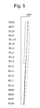
- FIG. 5 depicts a plot of memory hole diameter in the stack of FIG. 4 .
- the vertical axis is aligned with the stack of FIG. 4 and depicts a width (wMH), e.g., diameter, of the pillars formed by materials in the memory holes 618 and 619 .
- wMH width
- the memory holes which are etched through the stack have a very high aspect ratio. For example, a depth-to-diameter ratio of about 25-30 is common.
- the memory holes may have a circular cross-section. Due to the etching process, the memory hole and resulting pillar width can vary along the length of the hole. Typically, the diameter becomes progressively smaller from the top to the bottom of the memory hole (solid line in FIG. 5 ).
- the memory holes are tapered, narrowing at the bottom of the stack. In some cases, a slight narrowing occurs at the top of the hole near the select gate so that the diameter becomes slight wider before becoming progressively smaller from the top to the bottom of the memory hole (long dashed line in FIG. 5 ).
- the memory hole width is a maximum at the level of WL 9 in the stack, in this example. The memory hole width is slightly smaller at the level of WL 10 , and progressively smaller at the levels of WL 8 to WL 0 .
- the programming and erase speed of the memory cells can vary based on their position along the memory hole. With a relatively smaller diameter portion of a memory hole, the electric field across the tunnel oxide is relatively stronger, so that the programming and erase speed is higher.
- the stack is fabricated in two tiers.
- the stack can be fabricated in two or more tiers.
- the bottom tier is formed first with a respective memory hole.
- the top tier is then formed with a respective memory hole which is aligned with the memory hole in the bottom tier.
- Each memory hole is tapered such that a double tapered memory hole is formed in which the width increases, then decreases and increases again, moving from the bottom of the stack to the top.
- FIG. 6 depicts a close-up view of the region 622 of the stack of FIG. 4 .
- Memory cells are formed at the different levels of the stack at the intersection of a word line layer and a memory hole.
- memory cells 680 and 681 are formed in WLL 9 and WLL 10 , respectively.
- the memory cells are formed from films which are deposited along the sidewall (SW) of the memory hole 630 and/or within each word line layer, e.g., using atomic layer deposition.
- each column (e.g., the pillar which is formed by the materials within a memory hole) can include a blocking oxide layer 660 , charge-trapping layer 663 such as Si 3 N 4 or other nitride, a tunneling oxide layer 664 , a channel layer 665 (e.g., comprising polysilicon), and a dielectric core 666 .
- the blocking oxide may comprises a continuous oxide layer such as silicon dioxide along the sidewall, in one approach.
- the charge-trapping layer, tunneling oxide layer and channel may also comprise continuous layers along the sidewall, in one approach.
- a word line layer can include a metal barrier 670 a (e.g., TiN, TaN, a nitride based metal barrier layer or a non-nitride metal barrier layer such as Ti or CoW) and a control gate metal 662 (e.g., W, Co, Ti, Ru or Ta) as a control gate.
- a metal barrier 670 a e.g., TiN, TaN, a nitride based metal barrier layer or a non-nitride metal barrier layer such as Ti or CoW
- control gate metal 662 e.g., W, Co, Ti, Ru or Ta
- control gates 691 and 690 are provided in WLL 9 and WLL 10 , respectively.
- a word line layer can also include a high-k block oxide layer 670 such as aluminum oxide (Al 2 O 3 ). Additional pillars are similarly formed in the different memory holes.
- a pillar can form a columnar active area (AA) of a NAND string.
- the device can be considered to be a metal-aluminum-nitride-oxide-silicon (MANOS) memory device, where the metal is the control gate metal 662 , the aluminum is the aluminum oxide of the high-k block oxide layer 670 , the nitride is the charge-trapping layer 663 such as Si 3 N 4 or other nitride, the oxide is the tunnel oxide layer stack comprising oxide-nitride-oxide such as SiO 2 /SiO x N y /SiO 2 and the silicon is the channel layer 665 (e.g., comprising polysilicon).
- MANOS metal-aluminum-nitride-oxide-silicon
- the blocking oxide layer 660 includes portions which are adjacent to, and span a height of, the control gate layers and the dielectric layers. The height is along the vertical or z-axis.
- the charge-trapping layer 663 includes portions which are adjacent to, and span a height of, the control gate layers and the dielectric layers.
- an electric field is created by the program voltage which is applied to the control gate of a selected word line and by the pass voltage which is applied to the control gates of unselected word lines.
- the electric field includes fringing electric field paths 650 f 1 and 650 f 2 and a non-fringing electric field path 650 nf .
- Corresponding electric field portions are also depicted for WLL 9 .
- the electric field can occur when Vpgm or Vpass is applied to a control gate.
- Electrons, e.g., electron 651 are represented by circles with a horizontal line. Electrons are drawn into a portion of the charge-trapping layer which is adjacent to the control gate layer by the non-fringing electric field path 650 nf to program the memory cell 681 .
- the parasitic cells 680 or 681 When the memory cells 680 or 681 are sensed, such as during a read operation or program-verify operation, the parasitic cells will result in a resistance which distorts the sensing and can cause program disturb.
- the usual read pass voltage which is applied to the unselected word lines may not be high enough to provide the parasitic cells in a conductive state.
- the severity of the problem of parasitic cells depends on the strength of the fringing electric field. As discussed further below, e.g., in FIG. 10C , the fringing field can be affected by an inadvertent rounding off of the control gates.
- each of the memory holes can be filled with a plurality of annular layers comprising a blocking oxide layer, a charge-trapping layer, a tunneling layer and a channel layer.
- a core region of each of the memory holes is filled with a body material, and the plurality of annular layers are between the core region and the word line in each of the memory holes.
- the NAND string can be considered to have a floating body channel because the length of the channel is not formed on a substrate. Further, the NAND string is provided by a plurality of word line layers above one another in a stack, and separated from one another by dielectric layers.
- FIG. 7A depicts example Vth distributions of memory cells, where two data states are used.
- the final Vth distribution can be achieved by using one or more programming passes. Each pass may use incremental step pulse programming, for instance.
- program-verify iterations are performed for a selected word line.
- a program-verify iteration comprises a program portion in which a program voltage is applied to the word line followed by a verify portion in which one or more verify tests are performed.
- Each programmed state has a verify voltage which is used in the verify test for the state.
- a Vth distribution 700 represents an erased state (Eslc) and a Vth distribution 701 represents a programmed data state (Pslc), in an example of single-level cell (SLC) programming.
- the erased state may represent a one bit while the programmed state represents a zero bit, for example.
- a verify voltage for the programmed state is VvSLC and a read voltage for distinguishing between the two states is VrSLC.
- a read voltage for distinguishing between adjacent states e.g., a lower state and a higher state, should be located midway between the expected upper tail of the Vth distribution of the lower state and the expected lower tail of the Vth distribution of the higher state.
- FIG. 7B depicts example Vth distributions of memory cells, where four data states are used.
- the data states are represented by Vth distributions 710 , 711 , 712 and 713 for the Er, A, B and C states, respectively, and an example encoding of bits for each state is 11, 10, 00 and 01, respectively, in the format of upper page (UP) bit/lower page (LP) bit.
- the verify voltages are VvA, VvB and VvC
- the read voltages are VrA, VrB and VrC.
- a LP read may use VrA and VrC and an UP read may use VrB.
- FIG. 7 C 1 depicts example Vth distributions of memory cells, where eight data states are used.
- the verify voltages of the A, B, C, D, E, F and G states are VvA, VvB, VvC, VvD, VvE, VvF and VvG, respectively.
- a first set of read voltages for the A, B, C, D, E, F and G states includes VrA, VrB, VrC, VrD, VrE, VrF and VrG, respectively.
- an example encoding of bits for each state is 111, 110, 100, 000, 010, 011, 001 and 101, respectively.
- the ideal data states are represented by Vth distributions 720 , 721 , 722 , 723 , 724 , 725 , 726 and 727 for the Er, A, B, C, D, E, F and G states, respectively.
- the Vth distributions are widened and upshifted.
- the data states are represented by Vth distributions 720 a , 721 a , 722 a , 723 a , 724 a , 725 a , 726 a and 727 a for the Er, A, B, C, D, E, F and G states, respectively.
- the lower states experience a relatively larger upshift and widening in Vth, since more neighboring word line interference occurs.
- Vth distributions of cells on WLn were measured before (solid lines) and after (dashed lines) programming of cells on WLn+1.
- the cells on WLn+1 are programmed to randomly selected data states.
- the Vth width becomes significantly wider for the WLn cells after the WLn+1 cells are programmed.
- FIG. 7 C 2 depicts example upshifts in the Vth distribution of WLn memory cells according to the programmed state of WLn+1 memory cells.
- the WLn memory cells are in the A state.
- the Vth distribution becomes progressively higher as the data state of the cells on WLn+1 becomes progressively higher.
- the WLn+1 cells are programmed after the WLn cells.
- Vth distributions 750 , 751 , 752 , 753 , 754 , 755 , 756 and 757 correspond to the WLn+1 cells being in the Er, A, B, C, D, E, F or G states, respectively. This shows that the Vth upshift of the cells on WLn due to parasitic cells is a function of the data state of the WLn+1 cells.
- FIG. 7D depicts example Vth distributions of memory cells, where sixteen data states are used. Programming using four bits per cell (16 levels) can involve lower, lower-middle, upper-middle and upper pages.
- the data states are represented by Vth distributions 730 , 731 , 732 , 733 , 734 , 735 , 736 , 737 , 738 , 739 , 740 , 741 , 742 , 743 , 744 and 745 for the S0, S1, S2, S3, S4, S5, S6, S7, S8, S9, S10, S11, S12, S13, S14 and S15 states, respectively, and an example encoding of bits for each state is 1111, 1110, 1100, 1101, 1001, 1000, 1010, 1011, 0011, 0010, 0000, 0100, 0110, 0111, 0101 and 0001, respectively, in the format of upper page (UP) bit/upper middle (UMP) page bit, lower middle (LMP)
- the verify voltages are VvS 1 , VvS 2 , VvS 3 , VvS 4 , VvS 5 , VvS 6 , VvS 7 , VvS 8 , VvS 9 , VvS 10 , VvS 11 , VvS 12 , VvS 13 , VvS 4 and VvS 15 .
- the read voltages are VrS 1 , VrS 2 , VrS 3 , VrS 4 , VrS 5 , VrS 6 , VrS 7 , VrS 8 , VrS 9 , VrS 10 , VrS 11 , VrS 12 , VrS 13 , VrS 4 and VrS 15 .
- a LP read may use VrS 1 , VrS 3 , VrS 5 , VrS 7 , VrS 9 and VrS 13 .
- a LMP read may use VrS 2 , VrS 6 , VrS 10 , VrS 12 and VrS 14 .
- An UMP read may use VrS 4 , VrS 11 and VrS 15 .
- An UP read may use VrS 8 .
- FIG. 8 depicts an example process for fabricating a memory device with reduced neighboring word line interference.
- Step 800 includes forming a stack comprising alternating dielectric layers and control gate layers on a substrate.
- the control gate layers initially comprise a sacrificial material such as Si 3 N 4 . See, e.g., FIG. 9A .
- Step 801 includes etching memory holes in the stack. See, e.g., FIG. 9B .
- step 801 a is used to provide an etchant in the memory holes to recess the control gate layers. See, e.g., FIG. 13 .
- This step may include providing an etchant in the memory hole to recess the sacrificial material before providing the amorphous silicon layer along the sidewall.
- the etchant can be a wet or dry etchant which is more selective of the sacrificial material of the control gate layer than of the dielectric layers.
- a wet etch uses a liquid-phase etchant such as diluted hydrofluoric acid.
- a dry etch uses a plasma-phase etchant.
- the source gas for the plasma may comprise trifluoromethane.
- Example tools for a dry etch include SiconiTM process, chemical dry etching (CDE) and the FrontierTM system of Applied Materials, Inc.
- SiconiTM refers to a class of remote plasma assisted dry etch processes which involve the simultaneous exposure of a substrate to hydrogen- and fluorine-containing plasma effluents.
- Step 802 includes depositing amorphous silicon along the sidewalls of the memory holes, adjacent to the dielectric layers and control gate layers. See, e.g., FIG. 11A .
- the amorphous silicon layer may be a relatively thin layer, e.g., 3 nm, which is deposited conformally, e.g., conforming to the sidewall of the memory hole.
- the deposition comprises atomic layer deposition (ALD).
- one option at step 803 involves depositing an Si 3 N 4 layer along the amorphous silicon layer. See, e.g., FIG. 11B .
- the Si 3 N 4 layer is deposited, e.g., as a thin or flat nitride layer, it is oxidized to convert it to, e.g., an SiO 2 layer which serves as a blocking oxide layer.
- the Si 3 N 4 layer may be deposited using ALD or chemical-vapor deposition (CVD), for instance.
- the Si 3 N 4 is partially and not fully oxidized so that a composite of SiO x N y is formed, where N is in a relatively low concentration.
- the Si 3 N 4 layer may have a thickness of 3 nm or less to ensure it is fully oxidized.
- wet or dry oxidation can be used.
- Example of wet oxidation include in-situ steam generation (IS SG) and water vapor generation. Steam such as pyrogenic steam can be produced by burning hydrogen and oxygen in an oxidation furnace.
- Examples of dry oxidation include plasma isotropic oxidation, rapid plasma oxidation and Slot Plane Antenna (SPA) plasma generating technology.
- the oxidation can include a heating step at, e.g., 350 C or higher.
- Another option for oxidation for the Si 3 N 4 or the amorphous silicon is radical oxidation, which is a combination of wet and dry oxidation.
- Si 3 N 4 can be transformed to SiO 2 by the following formula in air or oxygen: Si 3 N 4 +3O 2 ⁇ 3SiO 2 +2N 2 .
- nitrogen (N 2 ) is a byproduct.
- Si 3 N 4 in the presence of high-pressure H 2 O, Si 3 N 4 can be transformed to SiO 2 by the following formula: Si 3 N 4 +6H 2 O ⁇ 3SiO 2 +4NH 3 .
- ammonia (NH 3 ) comprising nitrogen and hydrogen, is a byproduct.
- wet oxidation of the Si 3 N 4 layer can result in better quality and uniformity in the oxide but dry oxidation is also possible.
- the wet oxidation can involve a water molecule such as steam which provides high energy oxide radicals that interact with the Si 3 N 4 and break the Si—N bonds. The nitrogen is carried away while the oxygen bonds with the Si, creating SiO 2 .
- Step 803 can involve depositing a material comprising silicon in the memory hole, adjacent to the amorphous silicon layer, oxidizing the material comprising silicon in the memory hole to provide a material comprising oxidized silicon, wherein the material comprising oxidized silicon and the oxidized silicon layer formed in step 808 together form a blocking oxide layer.
- the material comprising silicon comprises Si 3 N 4
- the material comprising oxidized silicon comprises SiO 2
- the oxidized silicon layer comprises SiO 2 .
- step 804 Another option at step 804 is to deposit the SiO 2 directly as a blocking oxide layer, e.g., using ALD. This approach does not involve a conversion from Si 3 N 4 to SiO 2 . Generally, a high quality SiO 2 can be obtained via oxidation using step 803 while step 804 may be easier.
- Step 804 can involve depositing a material comprising oxidized silicon in the memory hole, adjacent to the amorphous silicon layer, wherein the material comprising oxidized silicon and the oxidized silicon layer together form a blocking oxide layer. Further, the material comprising oxidized silicon may comprise SiO 2 and the oxidized silicon layer may comprise SiO 2 .
- Step 805 includes depositing, in turn, a charge-trapping layer, a tunnel oxide and a channel layer along the sidewalls of the memory holes. See, e.g., FIGS. 9C and 11C .
- a dielectric core such as SiO 2 is also provided to fill a remainder of the memory holes.
- Step 806 includes etching a slit in the stack. See, e.g., FIG. 9D .
- Step 807 includes providing an etchant in the slit to remove the sacrificial material of the control gate layers, thus exposing portions of the amorphous silicon layer. See, e.g., FIG. 11C .
- the sacrificial material may comprise Si 3 N 4 and the dielectric layers may comprise oxide.
- the etchant can be a wet or dry etchant which is more selective of the sacrificial material of the control gate layer than of the dielectric layers.
- Step 808 includes oxidizing the amorphous silicon via the slits and voids. See, e.g., FIGS. 9D and 11D .
- the oxidizing of the amorphous silicon layer provides an oxidized silicon layer, e.g., SiO 2 , and the oxidizing comprises supplying oxygen via the slit and voids.
- a wet or dry oxidation may be used, as discussed. Wet oxidation of the amorphous silicon layer can result in better quality and uniformity in the oxide compared to dry oxidation. Further, the oxidation may be complete, resulting in SiO 2 .
- the degree of oxidation of the amorphous silicon depends on the thickness of the layer. A thicker film, e.g., more than 3 nm thick, will have a lower degree of oxidation. A thinner film, e.g., 3 nm or less, will generally be completely oxidized.
- the oxidizing agent can migrate to reach the portions of the amorphous silicon layer which are at the heights of the dielectric layers.
- the formula for converting amorphous silicon to SiO 2 is: Si+O 2 ⁇ SiO 2 . In this case, there is no gaseous byproduct.
- the formula for converting amorphous silicon to SiO 2 is: Si+2H 2 O ⁇ SiO 2 +2H 2 . In this case, hydrogen (H 2 ) is a byproduct.
- Step 809 includes depositing a control gate metal in the voids and closing the slit. See, e.g., FIGS. 9F, 9G and 11E .
- the SiO 2 layer formed from amorphous silicon can differ from the SiO 2 layer formed from Si 3 N 4 or directly deposited in the memory hole.
- the two SiO 2 layers can be distinguished by atomic percentage of hydrogen using an elemental analysis method. Hydrogen can be present in the two SiO 2 layers as a byproduct.
- the SiO 2 layer formed from amorphous silicon in step 808 will have a lower percentage of atomic hydrogen than the SiO 2 formed from oxidizing Si 3 N 4 in step 803 .
- the amorphous silicon may be converted to SiO 2 at a relatively high temperature such as >800 C, such that atomic hydrogen is driven away from the converted SiO 2 layer.
- the atomic percentage of hydrogen is H1%.
- the atomic hydrogen may originate from precursors such as SiH 2 Cl 2 (dichlorosilane).
- SiO 2 may be converted from Si 3 N 4 at a relatively low temperature such as ⁇ 800 C, such that a certain percentage of hydrogen (H2%) remains in the film and is not driven out.
- An example precursor is SiH 2 Cl 2 .
- SiCl 4 is used as a precursor for Si 3 N 4 deposition, Cl remain in the film.
- the SiO 2 layer formed from amorphous silicon in step 808 may also have a lower percentage of atomic hydrogen than the SiO 2 which is deposited by ALD or CVD in step 804 .
- ALD may be performed at a relatively low temperature such as ⁇ 500 C, so that the hydrogen content (H3%) is relatively high in films deposited using ALD.
- Films deposited using low-pressure CVD (LPCVD) may have a maximum deposition temperature of 780 C, for example.
- SiH 2 Cl 2 may be used as a precursor. Since the temperature is less than 800 C, the percentage of hydrogen (H4%) is higher than in the SiO 2 obtained from converted amorphous silicon.
- step 810 includes converting the channel polysilicon to single crystal silicon through heating, e.g., at 900 C.
- Single crystal silicon has a lower density of interface traps and no grain boundaries. This can improve Vth distribution widths, electron mobility, cell current, subthreshold slope, short-term data retention and temperature-based Vth shifts.
- step 810 could occur earlier in the process.
- step 807 could occur later in the process.
- Step 805 can include providing a charge-trapping layer, a tunneling layer, and a channel layer in the memory holes, after the providing the amorphous silicon layer along the sidewall in step 802 and before the oxidizing the amorphous silicon layer in step 808 . Further, providing the channel layer in step 805 can comprise depositing polysilicon adjacent to the tunneling layer and heating the polysilicon to form single crystal silicon consistent with step 810 .
- FIG. 9A depicts an example cross-sectional view of a stack of a memory device during a fabrication process consistent with step 800 of FIG. 8 , where the stack includes alternating dielectric and control gate layers.
- the dielectric layers may comprise oxide and the control gate layers may comprise Si 3 N 4 , for example, at this stage.
- the stack includes a substrate 611 and an insulating film 612 on the substrate.
- FIG. 9B depicts an example cross-sectional view of the stack of FIG. 9A after memory holes are formed, consistent with step 801 of FIG. 8 .
- a region 950 of the stack is discussed in FIG. 10A .
- the memory holes may be formed by etching.
- FIG. 9C depicts an example cross-sectional view of the stack of FIG. 9B after films 655 are deposited in the memory holes, consistent with steps 802 - 805 of FIG. 8 .
- the materials can include a blocking oxide layer, a charge-trapping layer, a tunneling layer, a channel layer and a dielectric core.
- FIG. 9D depicts an example cross-sectional view of the stack of FIG. 9C after slits 671 and 672 are formed in the stack, consistent with step 806 of FIG. 8 .
- the slits may be formed by etching and may extend along the z-axis and the x-axis along the stack.
- a region 951 of the stack is discussed in FIGS. 10D, 11E, 11F and 12B .
- Sacrificial material 955 of the control gate layers is depicted.
- Material 956 of the dielectric layers is also depicted.
- FIG. 9E depicts an example cross-sectional view of the stack of FIG. 9D after the sacrificial material 955 of the control gate layers is removed by providing an etchant in the slit, consistent with step 807 of FIG. 8 .
- Voids 955 a of the control gate layers are depicted.
- FIG. 9F depicts an example cross-sectional view of the stack of FIG. 9E after depositing a metal in the control gate layers via the slit, consistent with step 809 of FIG. 8 .
- the metal includes portions such as the portion 957 b which fills the voids of the control gate layers, and a portion 957 a which lines the slit.
- FIG. 9G depicts an example cross-sectional view of the stack of FIG. 9F after cleaning and filling in the slit, consistent with step 809 of FIG. 8 .
- the metal which lines the slit is cleaned away to avoid short circuiting the control gate layers.
- an insulating liner 958 such as SiO 2 is deposited in the slit and the bottom of the liner is etched through.
- An adhesion layer such as titanium nitride (TiN) may be deposited before the metal 959 .
- TiN titanium nitride
- the metal forms a continuous conductive path from a bottom of the stack to the top of the stack and can therefore act as a local interconnect. Interconnects 671 a and 672 a are formed.
- FIG. 10A depicts the region 950 of the stack of FIG. 9B after the formation of a memory hole, consistent with step 801 of FIG. 8 .
- the portion includes the dielectric layers DL 13 , DL 14 and DL 15 (including dielectric material 1006 ) and the control gates 691 and 690 in the word line layers WLL 9 and WLL 10 , respectively.
- a sidewall SW of the memory hole is also depicted.
- FIG. 10B depicts the region of the stack of FIG. 10A after depositing a layer of Si 3 N 4 1020 along a sidewall of the memory hole, in a comparative example.
- FIG. 10C depicts the region of the stack of FIG. 10B after an oxidizing step which converts the layer of Si 3 N 4 to a layer of SiO 2 1021 .
- the oxidizing step involves providing oxygen, depicted by circles 1023 , which migrates in the memory hole and interact with the Si 3 N 4 layer to form the SiO 2 layer.
- the oxidizing step can inadvertently oxidize portions of the Si 3 N 4 of the control gate layers. For example, corner portions 690 a and 690 b of the control gate 690 are oxidized. This phenomenon is also referred to as “gate bite.” As a result, the length of the channel of the memory cell is reduced from h 1 to h 2 .
- control gate 1022 in which the oxidized portion 1022 a extends a height h 1 of the control gate.
- Portions of the Si 3 N 4 of the control gate layers can also be inadvertently oxidized when an SiO 2 layer is deposited directly to provide the blocking oxide layer, rather than depositing Si 3 N 4 and then oxidizing it.
- FIG. 10D depicts the region of the stack of FIG. 10C after filling in a remainder of the memory hole with a charge-trapping layer 663 , a tunneling oxide layer 664 , a channel layer 665 and a dielectric core 666 .
- FIG. 11A depicts the region of the stack of FIG. 10A , after depositing a layer of amorphous silicon 1120 along a sidewall of the memory hole followed by a layer of Si 3 N 4 1121 , consistent with steps 802 and 803 of FIG. 8 .
- FIG. 11B depicts the region of the stack of FIG. 11A , after oxidizing the Si 3 N 4 to form a layer comprising SiO 2 1121 a , consistent with step 803 of FIG. 8 .
- the oxidizing step involves providing oxygen, depicted by circles, which migrates in the memory hole and interact with the Si 3 N 4 layer to form the SiO 2 layer.
- the amorphous silicon layer 1120 advantageously shields the Si 3 N 4 of the control gate layers from being oxidized.
- FIG. 11C depicts the region of the stack of FIG. 11B consistent with steps 805 - 807 of FIG. 8 , where portions of the amorphous silicon layer are exposed by removing a sacrificial material in the control gate layers.
- the memory hole is filled by the charge-trapping layer 663 , tunneling oxide layer 664 , channel layer 665 and the dielectric core 666 .
- the sacrificial material of the control gate layers is removed such that voids, e.g., void 1210 , are formed in the control gate layers.
- portions, e.g., portion 690 c of the amorphous silicon layer 1120 are exposed in the void.
- FIG. 11D depicts the region of the stack of FIG. 11C consistent with step 808 of FIG. 8 , where the amorphous silicon layer is oxidized.
- the oxidizing step involves providing oxygen, depicted by circles, which migrates in the voids via the slit and interacts with the amorphous silicon layer to form an SiO 2 layer 1120 a .
- the two layers together serve as a blocking oxide layer 1125 for the memory cells.
- the two layers have a similar thickness or width in the y-direction.
- the two layers each have a thickness of about 3 nm for a total block oxide thickness of 6 nm.
- a thickness of the oxidized amorphous silicon layer 1120 a may be within +/ ⁇ 30% of a thickness of the SiO 2 layer 1121 a , which is a material comprising oxidized silicon.
- FIG. 11E depicts the region of the stack of FIG. 11D consistent with step 809 of FIG. 8 , where the control gate metal is deposited.
- An example metal portion 690 d is part of the control gate layer 690 , for instance.
- the corners of the metal portion are advantageously not rounded off so that the performance of the memory device is improved.
- the oxidized amorphous silicon layer provides a high quality block oxide layer. The resulting memory device has an improved operation, program and erase efficiency and reliability.
- FIG. 11F depicts the region of the stack of FIG. 11D consistent with step 810 of FIG. 8 , where the channel polysilicon layer is converted to a single crystal silicon layer 665 through heating.
- FIG. 12A depicts an alternative to FIG. 11E , where an amorphous silicon layer 1120 b is provided adjacent to the charge-trapping layer 663 .
- the amorphous silicon layer alone is used to provide the blocking oxide layer.
- the amorphous silicon layer can be thicker than in the examples of FIG. 11E or 11F , for instance.
- FIG. 12B depicts the region of the stack of FIG. 12A , where the amorphous silicon layer is converted to an SiO 2 layer 1120 c .
- the process for obtaining the example structure of FIGS. 12A and 12B follows the example of FIG. 11A to 11F except the Si 3 N 4 layer 1121 is not provided in FIG. 11A .
- FIG. 13 depicts an alternative to FIG. 11E, 11F or 12B , where the control gate layers are recessed.
- the example control gate 690 d has a recess 690 e which is formed by providing an etchant in the memory hole.
- the example control gate 691 a similarly has a recess.
- the subsequent layers are conformally deposited.
- the recess in the control gate layer increases the distance between the control gate and the channel region between the word line layers, so that the fringing electric field between the control gate and the channel region between the word line layers is weakened.
- the distance between the control gate and the channel region adjacent to the control gate, at the same height in the stack, is not affected because a portion 665 a of the channel is shifted according to the recess of the control gate layer.
- the layers include a first SiO 2 layer 1120 d formed from amorphous silicon, a second SiO 2 layer 1121 d (formed by oxidizing Si 3 N 4 or deposited as SiO 2 using ALD), a charge-trapping film ( 663 ), a tunneling film ( 664 ) and a silicon channel film ( 665 ).
- a dielectric core 666 is also depicted.
- a method comprises: forming a stack of alternating dielectric layers and control gate layers, the control gate layers comprising a sacrificial material; forming a memory hole which extends through the stack, the memory hole comprising a sidewall; depositing an amorphous silicon layer along the sidewall, adjacent to the control gate layers; forming a slit in the stack; providing an etchant in the slit to remove the sacrificial material, creating voids in the control gates layers and exposing portions of the amorphous silicon layer; oxidizing the amorphous silicon layer to provide an oxidized silicon layer, the oxidizing comprises supplying oxygen via the slit and voids; and providing a metal in the voids, after the oxidized silicon layer is formed.
- an apparatus consistent with FIGS. 11E, 11F and 13 comprises: a stack of alternating dielectric layers and control gate layers, the control gate layers comprising a metal; and concentric films which extend through the stack, wherein the concentric films comprise a first oxidized film ( 1120 a , 1120 d ) adjacent to the control gate layers and the dielectric layers, a second oxidized film ( 1121 a , 1121 d ) adjacent to the first oxidized film, a charge-trapping film ( 663 ), a tunneling film ( 664 ) and a silicon channel film ( 665 , 665 a ).
- a method comprises: depositing an amorphous silicon layer along a sidewall of a memory hole in a stack, the stack comprising alternating oxide and nitride layers; removing the nitride layers via another opening in the stack, creating voids and exposing portions of the amorphous silicon layer; providing oxygen via the voids to oxidize the amorphous silicon layer, providing an oxidized silicon layer; and providing a metal in the voids, after the oxidized silicon layer is formed.
Abstract
Techniques for fabricating a memory device which has reduced neighboring word line interference, and a corresponding memory device. The memory device comprises a stack of alternating conductive and dielectric layers, where the conductive layers form word lines or control gates of memory cells. In one aspect, rounding off of the control gate layers due to inadvertent oxidation during fabrication is avoided. An amorphous silicon layer is deposited along the sidewall of the memory holes, adjacent to the control gate layers. Si3N4 is deposited along the amorphous silicon layer and oxidized in the memory hole to form SiO2. The amorphous silicon layer acts as an oxidation barrier for the sacrificial material of the control gate layers. The amorphous silicon layer is subsequently oxidized to also form SiO2. The two SiO2 layers together form a blocking oxide layer.
Description
The present technology relates to the operation of memory devices.
Semiconductor memory devices have become more popular for use in various electronic devices. For example, non-volatile semiconductor memory is used in cellular telephones, digital cameras, personal digital assistants, mobile computing devices, non-mobile computing devices and other devices.
A charge-storing material such as a floating gate or a charge-trapping material can be used in such memory devices to store a charge which represents a data state. A charge-trapping material can be arranged vertically in a three-dimensional (3D) stacked memory structure, or horizontally in a two-dimensional (2D) memory structure. One example of a 3D memory structure is the Bit Cost Scalable (BiCS) architecture which comprises a stack of alternating conductive and dielectric layers.
A memory device includes memory cells which may be arranged in strings, for instance, where select gate transistors are provided at the ends of the string to selectively connect a channel of the string to a source line or bit line. However, various challenges are presented in operating such memory devices.
FIG. 7C1 depicts example Vth distributions of memory cells, where eight data states are used.
FIG. 7C2 depicts example upshifts in the Vth distribution of WLn memory cells according to the programmed state of WLn+1 memory cells.
Techniques are provided for fabricating a memory device which has reduced neighboring word line interference. A corresponding memory device is also provided.
In some memory devices, memory cells are joined to one another such as in NAND strings in a block or sub-block. Each NAND string comprises a number of memory cells connected in series between one or more drain-side SG transistors (SGD transistors), on a drain-side of the NAND string which is connected to a bit line, and one or more source-side SG transistors (SGS transistors), on a source-side of the NAND string which is connected to a source line. Further, the memory cells can be arranged with a common control line (e.g., word line) which acts a control gate. A set of word lines extends from the source side of a block to the drain side of a block. Memory cells can be connected in other types of strings and in other ways as well.
The memory cells can include data memory cells, which are eligible to store user data, and dummy or non-data memory cells which are ineligible to store user data. A dummy word line is connected to a dummy memory cell. One or more dummy memory cells may be provided at the drain and/or source ends of a string of memory cells to provide a gradual transition in channel gradient.
During a programming operation, the memory cells are programmed according to a word line programming order. For example, the programming may start at the word line at the source side of the block and proceed to the word line at the drain side of the block. In one approach, each word line is completely programmed before programming a next word line. For example, a first word line, WL0, is programmed using one or more programming passes until the programming is completed. Next, a second word line, WL1, is programmed using one or more programming passes until the programming is completed, and so forth. A programming pass may include a set of increasing program voltages which are applied to the word line in respective program loops or program-verify iterations, such as depicted in FIG. 9 . Verify operations may be performed after each program voltage to determine whether the memory cells have completed programming. When programming is completed for a memory cell, it can be locked out from further programming while programming continues for other memory cells in subsequent program loops.
The memory cells may also be programmed according to a sub-block programming order, where memory cells in one sub-block, or portion of a block, are programmed before programming memory cells in another sub-block.
Each memory cell may be associated with a data state according to write data in a program command. Based on its data state, a memory cell will either remain in the erased state or be programmed to a programmed data state. For example, in a one bit per cell memory device, there are two data states including the erased state (Eslc) and the programmed state (Pslc) (see FIG. 7A ). In a two-bit per cell memory device, there are four data states including the erased state and three higher data states referred to as the A, B and C data states (see FIG. 7B ). In a three-bit per cell memory device, there are eight data states including the erased state and seven higher data states referred to as the A, B, C, D, E, F and G data states (see FIG. 7C1). In a four-bit per cell memory device, there are sixteen data states including the erased state and fifteen higher data states. The data states may be referred to as the S0, S1, S2, S3, S4, S5, S6, S7, S8, S9, S10, S11, S12, S13, S14 and S15 data states (see FIG. 7D ) where S0 is the erased state.
After the memory cells are programmed, the data can be read back in a read operation. A read operation can involve applying a series of read voltages to a word line while sensing circuitry determines whether cells connected to the word line are in a conductive or non-conductive state. If a cell is in a non-conductive state, the Vth of the memory cell exceeds the read voltage. The read voltages are set at levels which are expected to be between the threshold voltage levels of adjacent data states.
In one approach, the memory device comprises a stack of alternating conductive and dielectric layers, where the conductive layers form word lines or control gates of memory cells. The memory cells may be in strings which extend vertically in the stack. Further, the memory cells may be formed by an annular layers of blocking oxide, charge-trapping material, tunnel oxide and channel polysilicon which extend in the stack. The layers may be arranged concentrically. When a program voltage is applied to a one of the word lines, and a pass voltage is applied to unselected word lines, an electric field is created which draws electrons from the channel layer into a portion of the charge-trapping material which is adjacent to the word line. When the amount of charge corresponds to a desired data state, the programming is completed.
However, the electric field includes a fringing or lateral component which can draw electrons from the channel layer into a portion of the charge-trapping material which is between word lines. Electrons can also move laterally within the charge-trapping layer from a portion which is adjacent to the word lines to a portion of the charge-trapping material which is between word lines. These electrons form a parasitic cell which does not store data. As different word lines are used for programming in the device, additional parasitic cells can be formed. The parasitic cells interfere with the ability to accurately program the cells and result in widened Vth distributions.
In particular, for a cell of a given word line WLn, the programming of the cell of the next word line WLn+ 1 will increase the Vth of the cell of WLn. Moreover, the increase is proportional to the amount by which the data state (Vth) of the cell of WLn+1 exceeds the data state (Vth) of the cell of WLn (in the same NAND string or other set of connected cells). The most interference or upshift in Vth will be experienced by a low state cell on WLn when there is a high state cell on WLn+ 1. Moreover, this problem will become worse as memory devices are scaled down in size and the space between cells decreases.
Techniques provided herein address the above and other issues. In one aspect, the memory device is provided with a reduced fringing electric field by avoiding a rounding off of the control gate layers which can occur during fabrication. In particular, the formation of the blocking oxide layer in the memory hole can result in inadvertent oxidation of portions of the sacrificial material of the control gate layers. By reducing or avoiding this inadvertent oxidation, the rounding off of the corners is avoided. Other benefits including reducing short-channel effects of the memory cells is formed. One approach involves depositing an amorphous silicon layer along the sidewall of the memory holes, adjacent to the control gate layers and dielectric layers. Subsequently, a material such as Si3N4 is deposited along the amorphous silicon layer and oxidized in the memory hole to form SiO2. The amorphous silicon layer acts as an oxidation barrier for the sacrificial material of the control gate layers, which may also comprise Si3N4.
The amorphous silicon layer is oxidized in a back-side process, by removing the sacrificial material of the control gate layers to form voids and introducing an oxidizing agent in the voids. The amorphous silicon may also be converted to SiO2, so that the two adjacent SiO2 layers form a blocking oxide layer. In one option, SiO2 is deposited on the amorphous silicon layer rather than being oxidized in the memory hole. In another option, the control gate layers are recessed. This increases the distance between the control gate and the channel region between the word line layers so that the fringing electric field is weakened. In another option, the channel polysilicon is converted to single crystal silicon.
Various other features and benefits are described below.
The memory structure can be 2D or 3D. The memory structure may comprise one or more array of memory cells including a 3D array. The memory structure may comprise a monolithic 3D memory structure in which multiple memory levels are formed above (and not in) a single substrate, such as a wafer, with no intervening substrates. The memory structure may comprise any type of non-volatile memory that is monolithically formed in one or more physical levels of arrays of memory cells having an active area disposed above a silicon substrate. The memory structure may be in a non-volatile memory device having circuitry associated with the operation of the memory cells, whether the associated circuitry is above or within the substrate.
The control circuitry 110 cooperates with the read/write circuits 128 to perform memory operations on the memory structure 126, and includes a state machine 112, an on-chip address decoder 114, and a power control module 116. The state machine 112 provides chip-level control of memory operations. A storage region 113 may be provided, e.g., for program and read parameters as described further below.
The on-chip address decoder 114 provides an address interface between that used by the host or a memory controller to the hardware address used by the decoders 124 and 132. The power control module 116 controls the power and voltages supplied to the word lines, select gate lines and bit lines during memory operations. It can include drivers for word lines, SGS and SGD transistors and source lines. The sense blocks can include bit line drivers, in one approach. An SGS transistor is a select gate transistor at a source end of a NAND string, and an SGD transistor is a select gate transistor at a drain end of a NAND string.
In some implementations, some of the components can be combined. In various designs, one or more of the components (alone or in combination), other than memory structure 126, can be thought of as at least one control circuit which is configured to perform the techniques described herein. For example, a control circuit may include any one of, or a combination of, control circuitry 110, state machine 112, decoders 114 and 132, power control module 116, sense blocks SBb, SB2, . . . , SBp, read/write circuits 128, controller 122, and so forth.
The off-chip controller 122 may comprise a processor 122 c, storage devices (memory) such as ROM 122 a and RAM 122 b and an error-correction code (ECC) engine 245. The ECC engine can correct a number of read errors.
The storage device comprises code such as a set of instructions, and the processor is operable to execute the set of instructions to provide the functionality described herein. Alternatively or additionally, the processor can access code from a storage device 126 a of the memory structure, such as a reserved area of memory cells in one or more word lines.
For example, code can be used by the controller to access the memory structure such as for programming, read and erase operations. The code can include boot code and control code (e.g., a set of instructions). The boot code is software that initializes the controller during a booting or startup process and enables the controller to access the memory structure. The code can be used by the controller to control one or more memory structures. Upon being powered up, the processor 122 c fetches the boot code from the ROM 122 a or storage device 126 a for execution, and the boot code initializes the system components and loads the control code into the RAM 122 b. Once the control code is loaded into the RAM, it is executed by the processor. The control code includes drivers to perform basic tasks such as controlling and allocating memory, prioritizing the processing of instructions, and controlling input and output ports.
Generally, the control code can include instructions to perform the functions described herein.
In one embodiment, the host is a computing device (e.g., laptop, desktop, smartphone, tablet, digital camera) that includes one or more processors, one or more processor readable storage devices (RAM, ROM, flash memory, hard disk drive, solid state memory) that store processor readable code (e.g., software) for programming the one or more processors to perform the methods described herein. The host may also include additional system memory, one or more input/output interfaces and/or one or more input/output devices in communication with the one or more processors.
Other types of non-volatile memory in addition to NAND flash memory can also be used.
Semiconductor memory devices include volatile memory devices, such as dynamic random access memory (“DRAM”) or static random access memory (“SRAM”) devices, non-volatile memory devices, such as resistive random access memory (“ReRAM”), electrically erasable programmable read only memory (“EEPROM”), flash memory (which can also be considered a subset of EEPROM), ferroelectric random access memory (“FRAM”), and magnetoresistive random access memory (“MRAM”), and other semiconductor elements capable of storing information. Each type of memory device may have different configurations. For example, flash memory devices may be configured in a NAND or a NOR configuration.
The memory devices can be formed from passive and/or active elements, in any combinations. By way of non-limiting example, passive semiconductor memory elements include ReRAM device elements, which in some embodiments include a resistivity switching storage element, such as an anti-fuse or phase change material, and optionally a steering element, such as a diode or transistor. Further by way of non-limiting example, active semiconductor memory elements include EEPROM and flash memory device elements, which in some embodiments include elements containing a charge storage region, such as a floating gate, conductive nanoparticles, or a charge storage dielectric material.
Multiple memory elements may be configured so that they are connected in series or so that each element is individually accessible. By way of non-limiting example, flash memory devices in a NAND configuration (NAND memory) typically contain memory elements connected in series. A NAND string is an example of a set of series-connected transistors comprising memory cells and SG transistors.
A NAND memory array may be configured so that the array is composed of multiple strings of memory in which a string is composed of multiple memory elements sharing a single bit line and accessed as a group. Alternatively, memory elements may be configured so that each element is individually accessible, e.g., a NOR memory array. NAND and NOR memory configurations are examples, and memory elements may be otherwise configured.
The semiconductor memory elements located within and/or over a substrate may be arranged in two or three dimensions, such as a 2D memory structure or a 3D memory structure.
In a 2D memory structure, the semiconductor memory elements are arranged in a single plane or a single memory device level. Typically, in a 2D memory structure, memory elements are arranged in a plane (e.g., in an x-y direction plane) which extends substantially parallel to a major surface of a substrate that supports the memory elements. The substrate may be a wafer over or in which the layer of the memory elements are formed or it may be a carrier substrate which is attached to the memory elements after they are formed. As a non-limiting example, the substrate may include a semiconductor such as silicon.
The memory elements may be arranged in the single memory device level in an ordered array, such as in a plurality of rows and/or columns. However, the memory elements may be arrayed in non-regular or non-orthogonal configurations. The memory elements may each have two or more electrodes or contact lines, such as bit lines and word lines.
A 3D memory array is arranged so that memory elements occupy multiple planes or multiple memory device levels, thereby forming a structure in three dimensions (i.e., in the x, y and z directions, where the z direction is substantially perpendicular and the x and y directions are substantially parallel to the major surface of the substrate).
As a non-limiting example, a 3D memory structure may be vertically arranged as a stack of multiple 2D memory device levels. As another non-limiting example, a 3D memory array may be arranged as multiple vertical columns (e.g., columns extending substantially perpendicular to the major surface of the substrate, i.e., in the y direction) with each column having multiple memory elements. The columns may be arranged in a 2D configuration, e.g., in an x-y plane, resulting in a 3D arrangement of memory elements with elements on multiple vertically stacked memory planes. Other configurations of memory elements in three dimensions can also constitute a 3D memory array.
By way of non-limiting example, in a 3D NAND memory array, the memory elements may be coupled together to form a NAND string within a single horizontal (e.g., x-y) memory device level. Alternatively, the memory elements may be coupled together to form a vertical NAND string that traverses across multiple horizontal memory device levels. Other 3D configurations can be envisioned wherein some NAND strings contain memory elements in a single memory level while other strings contain memory elements which span through multiple memory levels. 3D memory arrays may also be designed in a NOR configuration and in a ReRAM configuration.
Typically, in a monolithic 3D memory array, one or more memory device levels are formed above a single substrate. Optionally, the monolithic 3D memory array may also have one or more memory layers at least partially within the single substrate. As a non-limiting example, the substrate may include a semiconductor such as silicon. In a monolithic 3D array, the layers constituting each memory device level of the array are typically formed on the layers of the underlying memory device levels of the array. However, layers of adjacent memory device levels of a monolithic 3D memory array may be shared or have intervening layers between memory device levels.
2D arrays may be formed separately and then packaged together to form a non-monolithic memory device having multiple layers of memory. For example, non-monolithic stacked memories can be constructed by forming memory levels on separate substrates and then stacking the memory levels atop each other. The substrates may be thinned or removed from the memory device levels before stacking, but as the memory device levels are initially formed over separate substrates, the resulting memory arrays are not monolithic 3D memory arrays. Further, multiple 2D memory arrays or 3D memory arrays (monolithic or non-monolithic) may be formed on separate chips and then packaged together to form a stacked-chip memory device.
Associated circuitry is typically required for operation of the memory elements and for communication with the memory elements. As non-limiting examples, memory devices may have circuitry used for controlling and driving memory elements to accomplish functions such as programming and reading. This associated circuitry may be on the same substrate as the memory elements and/or on a separate substrate. For example, a controller for memory read-write operations may be located on a separate controller chip and/or on the same substrate as the memory elements.
One of skill in the art will recognize that this technology is not limited to the 2D and 3D exemplary structures described but covers all relevant memory structures within the spirit and scope of the technology as described herein and as understood by one of skill in the art.
In one possible approach, the length of the plane, in the x-direction, represents a direction in which signal paths to word lines extend in the one or more upper metal layers (a word line or SGD line direction), and the width of the plane, in the y-direction, represents a direction in which signal paths to bit lines extend in the one or more upper metal layers (a bit line direction). The z-direction represents a height of the memory device.
The stack includes a substrate 611, an insulating film 612 on the substrate, and a portion of a source line SL. NS1 has a source-end 613 at a bottom 614 of the stack and a drain-end 615 at a top 616 of the stack. Metal-filled slits 617 and 620 may be provided periodically across the stack as interconnects which extend through the stack, such as to connect the source line to a line above the stack. The slits may be used during the formation of the word lines and subsequently filled with metal. The metal in the slits is provided within an insulating liner 658 such as SiO2 which acts as a sidewall insulator. A portion of a bit line BL0 is also depicted. A conductive via 621 connects the drain-end 615 to BL0.
Due to the non-uniformity in the diameter of the memory hole and pillar, the programming and erase speed of the memory cells can vary based on their position along the memory hole. With a relatively smaller diameter portion of a memory hole, the electric field across the tunnel oxide is relatively stronger, so that the programming and erase speed is higher.
In another possible implementation, represented by the short dashed line, the stack is fabricated in two tiers. The stack can be fabricated in two or more tiers. The bottom tier is formed first with a respective memory hole. The top tier is then formed with a respective memory hole which is aligned with the memory hole in the bottom tier. Each memory hole is tapered such that a double tapered memory hole is formed in which the width increases, then decreases and increases again, moving from the bottom of the stack to the top.
A word line layer can include a metal barrier 670 a (e.g., TiN, TaN, a nitride based metal barrier layer or a non-nitride metal barrier layer such as Ti or CoW) and a control gate metal 662 (e.g., W, Co, Ti, Ru or Ta) as a control gate. For example, control gates 691 and 690 are provided in WLL9 and WLL10, respectively. A word line layer can also include a high-k block oxide layer 670 such as aluminum oxide (Al2O3). Additional pillars are similarly formed in the different memory holes. A pillar can form a columnar active area (AA) of a NAND string.
The device can be considered to be a metal-aluminum-nitride-oxide-silicon (MANOS) memory device, where the metal is the control gate metal 662, the aluminum is the aluminum oxide of the high-k block oxide layer 670, the nitride is the charge-trapping layer 663 such as Si3N4 or other nitride, the oxide is the tunnel oxide layer stack comprising oxide-nitride-oxide such as SiO2/SiOxNy/SiO2 and the silicon is the channel layer 665 (e.g., comprising polysilicon).
When a memory cell is programmed, electrons are stored in a portion of the charge-trapping layer which is associated with the memory cell. These electrons are drawn into the charge-trapping layer from the channel, and through the tunneling layer. The Vth of a memory cell is increased in proportion to (e.g., with an increase in) the amount of stored charge. During an erase operation, the electrons return to the channel.
The blocking oxide layer 660 includes portions which are adjacent to, and span a height of, the control gate layers and the dielectric layers. The height is along the vertical or z-axis. Similarly, the charge-trapping layer 663 includes portions which are adjacent to, and span a height of, the control gate layers and the dielectric layers.
During programming, an electric field is created by the program voltage which is applied to the control gate of a selected word line and by the pass voltage which is applied to the control gates of unselected word lines. For the control gate 690, the electric field includes fringing electric field paths 650 f 1 and 650 f 2 and a non-fringing electric field path 650 nf. Corresponding electric field portions are also depicted for WLL9. The electric field can occur when Vpgm or Vpass is applied to a control gate. Electrons, e.g., electron 651, are represented by circles with a horizontal line. Electrons are drawn into a portion of the charge-trapping layer which is adjacent to the control gate layer by the non-fringing electric field path 650 nf to program the memory cell 681.
However, a smaller but still detectable number of electrons are also drawn into the portions of the charge-trapping layer which are adjacent to the dielectric layers by the fringing electric field path 650 f 1 and 650 f 2, resulting in corresponding parasitic cells, e.g., parasitic cell PC. It is also possible for electrons which are in portions of the charge-trapping layer adjacent to the word lines to move laterally in the charge-trapping layer to portions of the charge-trapping layer adjacent to the dielectric layers, also contributing to the parasitic cells. This movement is represented by arrows 6501 f 1 and 6501 f 2. When the memory cells 680 or 681 are sensed, such as during a read operation or program-verify operation, the parasitic cells will result in a resistance which distorts the sensing and can cause program disturb. In particular, the usual read pass voltage which is applied to the unselected word lines may not be high enough to provide the parasitic cells in a conductive state.
The severity of the problem of parasitic cells depends on the strength of the fringing electric field. As discussed further below, e.g., in FIG. 10C , the fringing field can be affected by an inadvertent rounding off of the control gates.
As shown, each of the memory holes can be filled with a plurality of annular layers comprising a blocking oxide layer, a charge-trapping layer, a tunneling layer and a channel layer. A core region of each of the memory holes is filled with a body material, and the plurality of annular layers are between the core region and the word line in each of the memory holes.
The NAND string can be considered to have a floating body channel because the length of the channel is not formed on a substrate. Further, the NAND string is provided by a plurality of word line layers above one another in a stack, and separated from one another by dielectric layers.
A Vth distribution 700 represents an erased state (Eslc) and a Vth distribution 701 represents a programmed data state (Pslc), in an example of single-level cell (SLC) programming. The erased state may represent a one bit while the programmed state represents a zero bit, for example. A verify voltage for the programmed state is VvSLC and a read voltage for distinguishing between the two states is VrSLC. Generally, a read voltage for distinguishing between adjacent states, e.g., a lower state and a higher state, should be located midway between the expected upper tail of the Vth distribution of the lower state and the expected lower tail of the Vth distribution of the higher state.
FIG. 7C1 depicts example Vth distributions of memory cells, where eight data states are used. The verify voltages of the A, B, C, D, E, F and G states are VvA, VvB, VvC, VvD, VvE, VvF and VvG, respectively. A first set of read voltages for the A, B, C, D, E, F and G states includes VrA, VrB, VrC, VrD, VrE, VrF and VrG, respectively. For the A, B, C, D, E, F and G states, an example encoding of bits for each state is 111, 110, 100, 000, 010, 011, 001 and 101, respectively. The ideal data states are represented by Vth distributions 720, 721, 722, 723, 724, 725, 726 and 727 for the Er, A, B, C, D, E, F and G states, respectively. When the parasitic cells are present, the Vth distributions are widened and upshifted. In this case, the data states are represented by Vth distributions 720 a, 721 a, 722 a, 723 a, 724 a, 725 a, 726 a and 727 a for the Er, A, B, C, D, E, F and G states, respectively. As mentioned, the lower states experience a relatively larger upshift and widening in Vth, since more neighboring word line interference occurs.
In this experiment, the Vth distributions of cells on WLn were measured before (solid lines) and after (dashed lines) programming of cells on WLn+ 1. The cells on WLn+1 are programmed to randomly selected data states. The Vth width becomes significantly wider for the WLn cells after the WLn+1 cells are programmed.
FIG. 7C2 depicts example upshifts in the Vth distribution of WLn memory cells according to the programmed state of WLn+1 memory cells. In this example, the WLn memory cells are in the A state. The Vth distribution becomes progressively higher as the data state of the cells on WLn+ 1 becomes progressively higher. Recall that the WLn+1 cells are programmed after the WLn cells. Vth distributions 750, 751, 752, 753, 754, 755, 756 and 757 correspond to the WLn+1 cells being in the Er, A, B, C, D, E, F or G states, respectively. This shows that the Vth upshift of the cells on WLn due to parasitic cells is a function of the data state of the WLn+1 cells.
A LP read may use VrS1, VrS3, VrS5, VrS7, VrS9 and VrS13. A LMP read may use VrS2, VrS6, VrS10, VrS12 and VrS14. An UMP read may use VrS4, VrS11 and VrS15. An UP read may use VrS8.
Generally, a wet etch uses a liquid-phase etchant such as diluted hydrofluoric acid. A dry etch uses a plasma-phase etchant. For example, the source gas for the plasma may comprise trifluoromethane. Example tools for a dry etch include Siconi™ process, chemical dry etching (CDE) and the Frontier™ system of Applied Materials, Inc. Siconi™ refers to a class of remote plasma assisted dry etch processes which involve the simultaneous exposure of a substrate to hydrogen- and fluorine-containing plasma effluents.
Step 802 includes depositing amorphous silicon along the sidewalls of the memory holes, adjacent to the dielectric layers and control gate layers. See, e.g., FIG. 11A . The amorphous silicon layer may be a relatively thin layer, e.g., 3 nm, which is deposited conformally, e.g., conforming to the sidewall of the memory hole. In one approach, the deposition comprises atomic layer deposition (ALD).
Subsequently, one option at step 803 involves depositing an Si3N4 layer along the amorphous silicon layer. See, e.g., FIG. 11B . Once the Si3N4 layer is deposited, e.g., as a thin or flat nitride layer, it is oxidized to convert it to, e.g., an SiO2 layer which serves as a blocking oxide layer. The Si3N4 layer may be deposited using ALD or chemical-vapor deposition (CVD), for instance. In some cases, the Si3N4 is partially and not fully oxidized so that a composite of SiOxNy is formed, where N is in a relatively low concentration. The Si3N4 layer may have a thickness of 3 nm or less to ensure it is fully oxidized.
In the oxidation processes described herein, wet or dry oxidation can be used. Example of wet oxidation include in-situ steam generation (IS SG) and water vapor generation. Steam such as pyrogenic steam can be produced by burning hydrogen and oxygen in an oxidation furnace. Examples of dry oxidation include plasma isotropic oxidation, rapid plasma oxidation and Slot Plane Antenna (SPA) plasma generating technology. The oxidation can include a heating step at, e.g., 350 C or higher. Another option for oxidation for the Si3N4 or the amorphous silicon is radical oxidation, which is a combination of wet and dry oxidation.
Si3N4 can be transformed to SiO2 by the following formula in air or oxygen: Si3N4+3O2→3SiO2+2N2. In this case, nitrogen (N2) is a byproduct. Or, in the presence of high-pressure H2O, Si3N4 can be transformed to SiO2 by the following formula: Si3N4+6H2O→3SiO2+4NH3. In this case, ammonia (NH3), comprising nitrogen and hydrogen, is a byproduct.
Wet oxidation of the Si3N4 layer can result in better quality and uniformity in the oxide but dry oxidation is also possible. The wet oxidation can involve a water molecule such as steam which provides high energy oxide radicals that interact with the Si3N4 and break the Si—N bonds. The nitrogen is carried away while the oxygen bonds with the Si, creating SiO2.
Step 803 can involve depositing a material comprising silicon in the memory hole, adjacent to the amorphous silicon layer, oxidizing the material comprising silicon in the memory hole to provide a material comprising oxidized silicon, wherein the material comprising oxidized silicon and the oxidized silicon layer formed in step 808 together form a blocking oxide layer. In one approach, the material comprising silicon comprises Si3N4, the material comprising oxidized silicon comprises SiO2, and the oxidized silicon layer comprises SiO2.
Another option at step 804 is to deposit the SiO2 directly as a blocking oxide layer, e.g., using ALD. This approach does not involve a conversion from Si3N4 to SiO2. Generally, a high quality SiO2 can be obtained via oxidation using step 803 while step 804 may be easier. Step 804 can involve depositing a material comprising oxidized silicon in the memory hole, adjacent to the amorphous silicon layer, wherein the material comprising oxidized silicon and the oxidized silicon layer together form a blocking oxide layer. Further, the material comprising oxidized silicon may comprise SiO2 and the oxidized silicon layer may comprise SiO2.
Step 805 includes depositing, in turn, a charge-trapping layer, a tunnel oxide and a channel layer along the sidewalls of the memory holes. See, e.g., FIGS. 9C and 11C . A dielectric core such as SiO2 is also provided to fill a remainder of the memory holes.
Step 806 includes etching a slit in the stack. See, e.g., FIG. 9D . Step 807 includes providing an etchant in the slit to remove the sacrificial material of the control gate layers, thus exposing portions of the amorphous silicon layer. See, e.g., FIG. 11C . The sacrificial material may comprise Si3N4 and the dielectric layers may comprise oxide. The etchant can be a wet or dry etchant which is more selective of the sacrificial material of the control gate layer than of the dielectric layers. Step 808 includes oxidizing the amorphous silicon via the slits and voids. See, e.g., FIGS. 9D and 11D . The oxidizing of the amorphous silicon layer provides an oxidized silicon layer, e.g., SiO2, and the oxidizing comprises supplying oxygen via the slit and voids. A wet or dry oxidation may be used, as discussed. Wet oxidation of the amorphous silicon layer can result in better quality and uniformity in the oxide compared to dry oxidation. Further, the oxidation may be complete, resulting in SiO2. The degree of oxidation of the amorphous silicon depends on the thickness of the layer. A thicker film, e.g., more than 3 nm thick, will have a lower degree of oxidation. A thinner film, e.g., 3 nm or less, will generally be completely oxidized.
Although only the portions of the amorphous silicon layer which are at the heights of the control gate layers are exposed, the oxidizing agent can migrate to reach the portions of the amorphous silicon layer which are at the heights of the dielectric layers.
In a dry oxidation process, the formula for converting amorphous silicon to SiO2 is: Si+O2→SiO2. In this case, there is no gaseous byproduct. In a wet oxidation process, the formula for converting amorphous silicon to SiO2 is: Si+2H2O→SiO2+2H2. In this case, hydrogen (H2) is a byproduct.
Step 809 includes depositing a control gate metal in the voids and closing the slit. See, e.g., FIGS. 9F, 9G and 11E .
The SiO2 layer formed from amorphous silicon can differ from the SiO2 layer formed from Si3N4 or directly deposited in the memory hole. For example, the two SiO2 layers can be distinguished by atomic percentage of hydrogen using an elemental analysis method. Hydrogen can be present in the two SiO2 layers as a byproduct.
In one approach, the SiO2 layer formed from amorphous silicon in step 808 will have a lower percentage of atomic hydrogen than the SiO2 formed from oxidizing Si3N4 in step 803. The amorphous silicon may be converted to SiO2 at a relatively high temperature such as >800 C, such that atomic hydrogen is driven away from the converted SiO2 layer. The atomic percentage of hydrogen is H1%. The atomic hydrogen may originate from precursors such as SiH2Cl2 (dichlorosilane). On the other hand, SiO2 may be converted from Si3N4 at a relatively low temperature such as <800 C, such that a certain percentage of hydrogen (H2%) remains in the film and is not driven out. An example precursor is SiH2Cl2. Moreover, if SiCl4 is used as a precursor for Si3N4 deposition, Cl remain in the film.
The SiO2 layer formed from amorphous silicon in step 808 may also have a lower percentage of atomic hydrogen than the SiO2 which is deposited by ALD or CVD in step 804. ALD may be performed at a relatively low temperature such as ≦500 C, so that the hydrogen content (H3%) is relatively high in films deposited using ALD. Films deposited using low-pressure CVD (LPCVD) may have a maximum deposition temperature of 780 C, for example. SiH2Cl2 may be used as a precursor. Since the temperature is less than 800 C, the percentage of hydrogen (H4%) is higher than in the SiO2 obtained from converted amorphous silicon.
Thus, H2%>H1%, H3%>H1%, H4%>H1% and H4%>H3%, in example implementations.
Optionally, step 810 includes converting the channel polysilicon to single crystal silicon through heating, e.g., at 900 C. Single crystal silicon has a lower density of interface traps and no grain boundaries. This can improve Vth distribution widths, electron mobility, cell current, subthreshold slope, short-term data retention and temperature-based Vth shifts.
Note that the steps depicted in FIG. 8 can be performed in different orders in different implementations. For example, step 810 could occur earlier in the process. Also, step 807 could occur later in the process.
Step 805 can include providing a charge-trapping layer, a tunneling layer, and a channel layer in the memory holes, after the providing the amorphous silicon layer along the sidewall in step 802 and before the oxidizing the amorphous silicon layer in step 808. Further, providing the channel layer in step 805 can comprise depositing polysilicon adjacent to the tunneling layer and heating the polysilicon to form single crystal silicon consistent with step 810.
Portions of the Si3N4 of the control gate layers can also be inadvertently oxidized when an SiO2 layer is deposited directly to provide the blocking oxide layer, rather than depositing Si3N4 and then oxidizing it.
The layers include a first SiO2 layer 1120 d formed from amorphous silicon, a second SiO2 layer 1121 d (formed by oxidizing Si3N4 or deposited as SiO2 using ALD), a charge-trapping film (663), a tunneling film (664) and a silicon channel film (665). A dielectric core 666 is also depicted.
Accordingly, it can be seen that, in one embodiment, a method comprises: forming a stack of alternating dielectric layers and control gate layers, the control gate layers comprising a sacrificial material; forming a memory hole which extends through the stack, the memory hole comprising a sidewall; depositing an amorphous silicon layer along the sidewall, adjacent to the control gate layers; forming a slit in the stack; providing an etchant in the slit to remove the sacrificial material, creating voids in the control gates layers and exposing portions of the amorphous silicon layer; oxidizing the amorphous silicon layer to provide an oxidized silicon layer, the oxidizing comprises supplying oxygen via the slit and voids; and providing a metal in the voids, after the oxidized silicon layer is formed.
In another embodiment, an apparatus consistent with FIGS. 11E, 11F and 13 , for example, comprises: a stack of alternating dielectric layers and control gate layers, the control gate layers comprising a metal; and concentric films which extend through the stack, wherein the concentric films comprise a first oxidized film (1120 a, 1120 d) adjacent to the control gate layers and the dielectric layers, a second oxidized film (1121 a, 1121 d) adjacent to the first oxidized film, a charge-trapping film (663), a tunneling film (664) and a silicon channel film (665, 665 a).
In another embodiment, a method comprises: depositing an amorphous silicon layer along a sidewall of a memory hole in a stack, the stack comprising alternating oxide and nitride layers; removing the nitride layers via another opening in the stack, creating voids and exposing portions of the amorphous silicon layer; providing oxygen via the voids to oxidize the amorphous silicon layer, providing an oxidized silicon layer; and providing a metal in the voids, after the oxidized silicon layer is formed.
The foregoing detailed description of the invention has been presented for purposes of illustration and description. It is not intended to be exhaustive or to limit the invention to the precise form disclosed. Many modifications and variations are possible in light of the above teachings. The described embodiments were chosen in order to best explain the principles of the invention and its practical application, to thereby enable others skilled in the art to best utilize the invention in various embodiments and with various modifications as are suited to the particular use contemplated. It is intended that the scope of the invention be defined by the claims appended hereto.
Claims (14)
1. A method, comprising:
forming a stack of alternating dielectric layers and sacrificial material layers;
forming a memory hole which extends through the stack, the memory hole comprising a sidewall;
depositing an amorphous silicon layer along the sidewall, adjacent to the dielectric layers and the sacrificial material layers, from a bottom of the memory hole to a top of the memory hole;
depositing a material comprising silicon in the memory hole, adjacent to the amorphous silicon layer, from the bottom of the memory hole to the top of the memory hole;
oxidizing the material comprising silicon in the memory hole to provide a material comprising oxidized silicon;
forming a slit in the stack;
providing an etchant in the slit to remove the sacrificial material layers, creating voids which expose portions of the amorphous silicon layer at heights of the sacrificial material layers;
oxidizing the exposed portions of the amorphous silicon layer at the heights of the sacrificial material layers and portions of the amorphous silicon layer which are at heights of the dielectric layers to convert the amorphous silicon layer to an oxidized silicon layer extending from the bottom of the memory hole to the top of the memory hole, wherein the oxidizing comprises supplying oxygen via the slit and voids, and the oxidized silicon layer and the material comprising oxidized silicon together form a blocking oxide layer which extends from the bottom of the memory hole to the top of the memory hole; and
providing a metal in the voids, after the oxidized silicon layer is formed.
2. The method of claim 1 , wherein:
the material comprising silicon comprises Si3N4;
the material comprising oxidized silicon comprises SiO2; and
the oxidized silicon layer comprises SiO2.
3. The method of claim 1 , wherein:
the amorphous silicon layer comprises a film with a thickness of 3 nm or less and is completely oxidized by the oxidizing step.
4. The method of claim 1 , wherein:
the supplying oxygen via the slit and voids comprises performing a wet oxidation process.
5. The method of claim 1 , wherein:
the sacrificial material layers comprise Si3N4 and the dielectric layers comprise oxide.
6. The method of claim 1 , further comprising:
providing an etchant in the memory hole to recess the sacrificial material layers before the providing the amorphous silicon layer along the sidewall.
7. The method of claim 1 , further comprising:
providing a charge-trapping layer, a tunneling layer, and a channel layer in the memory holes, after the providing the amorphous silicon layer along the sidewall and before the oxidizing the amorphous silicon layer.
8. The method of claim 7 , wherein:
the providing the channel layer comprises depositing polysilicon adjacent to the tunneling layer and heating the polysilicon to form single crystal silicon.
9. The method of claim 1 , wherein:
the amorphous silicon layer is deposited along the sidewall, adjacent to the dielectric layers and the sacrificial material layers, with no other layer between the amorphous layer and the dielectric layers and the sacrificial material layers.
10. The method of claim 1 , wherein:
the oxygen is supplied by a wet oxidizing agent in the voids which migrates to reach the portions of the amorphous silicon layer which are at the heights of the dielectric layers.
11. The method of claim 1 , wherein:
the amorphous silicon layer shields the sacrificial material layers from being oxidized during the oxidizing of the material comprising silicon.
12. A method, comprising:
depositing an amorphous silicon layer along a sidewall of a memory hole in a stack, the stack comprising alternating oxide and nitride layers;
depositing a Si3N4 layer in the memory hole, adjacent to the amorphous silicon layer;
oxidizing the Si3N4 layer to form a first SiO2 layer;
after the oxidizing the Si3N4 layer, removing the nitride layers via another opening in the stack, creating voids and exposing portions of the amorphous silicon layer;
after the removing the nitride layers, providing oxygen via the voids to oxidize the amorphous silicon layer, thereby providing a second SiO2 layer extending from a bottom of the stack to a top of the stack, wherein the first SiO2 layer and the second SiO2 layer together form a blocking oxide layer extending from a bottom of the stack to a top of the stack; and
providing a metal in the voids, after the second SiO2 layer is formed.
13. The method of claim 12 , wherein:
an atomic percentage of hydrogen is lower in the second SiO2 layer than in the first SiO2 layer.
14. The method of claim 12 , wherein:
the amorphous silicon layer shields the nitride layers from being oxidized during the oxidizing of the Si3N4 layer.
Priority Applications (2)
| Application Number | Priority Date | Filing Date | Title |
|---|---|---|---|
| US15/190,574 US9859298B1 (en) | 2016-06-23 | 2016-06-23 | Amorphous silicon layer in memory device which reduces neighboring word line interference |
| PCT/US2017/018759 WO2017222605A1 (en) | 2016-06-23 | 2017-02-21 | Amorphous silicon layer in memory device which reduces neighboring word line interference |
Applications Claiming Priority (1)
| Application Number | Priority Date | Filing Date | Title |
|---|---|---|---|
| US15/190,574 US9859298B1 (en) | 2016-06-23 | 2016-06-23 | Amorphous silicon layer in memory device which reduces neighboring word line interference |
Publications (2)
| Publication Number | Publication Date |
|---|---|
| US20170373086A1 US20170373086A1 (en) | 2017-12-28 |
| US9859298B1 true US9859298B1 (en) | 2018-01-02 |
Family
ID=58266197
Family Applications (1)
| Application Number | Title | Priority Date | Filing Date |
|---|---|---|---|
| US15/190,574 Active US9859298B1 (en) | 2016-06-23 | 2016-06-23 | Amorphous silicon layer in memory device which reduces neighboring word line interference |
Country Status (2)
| Country | Link |
|---|---|
| US (1) | US9859298B1 (en) |
| WO (1) | WO2017222605A1 (en) |
Cited By (2)
| Publication number | Priority date | Publication date | Assignee | Title |
|---|---|---|---|---|
| US10748627B2 (en) | 2018-12-21 | 2020-08-18 | Sandisk Technologies Llc | Reducing neighbor word line interference in a two-tier memory device by modifying word line programming order |
| US11217602B2 (en) | 2019-06-10 | 2022-01-04 | SK Hynix Inc. | Memory device and method for fabricating the memory device |
Families Citing this family (28)
| Publication number | Priority date | Publication date | Assignee | Title |
|---|---|---|---|---|
| US9136128B2 (en) | 2011-08-31 | 2015-09-15 | Micron Technology, Inc. | Methods and apparatuses including memory cells with air gaps and other low dielectric constant materials |
| KR102629466B1 (en) * | 2016-09-21 | 2024-01-26 | 에스케이하이닉스 주식회사 | Manufacturing method of semiconductor device |
| US10446572B2 (en) | 2017-08-11 | 2019-10-15 | Micron Technology, Inc. | Void formation for charge trap structures |
| US10164009B1 (en) | 2017-08-11 | 2018-12-25 | Micron Technology, Inc. | Memory device including voids between control gates |
| US10680006B2 (en) | 2017-08-11 | 2020-06-09 | Micron Technology, Inc. | Charge trap structure with barrier to blocking region |
| US10453855B2 (en) | 2017-08-11 | 2019-10-22 | Micron Technology, Inc. | Void formation in charge trap structures |
| US10217795B1 (en) * | 2017-08-23 | 2019-02-26 | Sandisk Technologies Llc | Memory cell for non-volatile memory system |
| US10283562B2 (en) | 2017-08-23 | 2019-05-07 | Sandisk Technologies Llc | Process for fabricating three dimensional non-volatile memory system |
| US10249682B2 (en) | 2017-08-23 | 2019-04-02 | Sandisk Technologies Llc | Non-volatile memory system with serially connected non-volatile reversible resistance-switching memory cells |
| US10290642B2 (en) * | 2017-09-30 | 2019-05-14 | Intel Corporation | Flash memory devices incorporating a polydielectric layer |
| JP7074583B2 (en) * | 2018-06-26 | 2022-05-24 | キオクシア株式会社 | Semiconductor storage device |
| WO2020019149A1 (en) * | 2018-07-24 | 2020-01-30 | Yangtze Memory Technologies Co., Ltd. | Three-dimensional memory device with corrosion-resistant composite spacer |
| US10720444B2 (en) | 2018-08-20 | 2020-07-21 | Sandisk Technologies Llc | Three-dimensional flat memory device including a dual dipole blocking dielectric layer and methods of making the same |
| JP2020035799A (en) * | 2018-08-27 | 2020-03-05 | キオクシア株式会社 | Semiconductor storage device |
| KR20200141841A (en) * | 2019-06-11 | 2020-12-21 | 에스케이하이닉스 주식회사 | Semiconductor device and method of manufacturing the same |
| JP2021034522A (en) * | 2019-08-22 | 2021-03-01 | キオクシア株式会社 | Semiconductor storage device |
| JPWO2021094844A1 (en) * | 2019-11-11 | 2021-05-20 | ||
| US11271006B2 (en) * | 2019-12-05 | 2022-03-08 | Micron Technology, Inc. | Methods of forming charge-blocking material, and integrated assemblies having charge-blocking material |
| KR20220123288A (en) * | 2020-01-03 | 2022-09-06 | 시놉시스, 인크. | Electro-thermal Method for Fabricating Monocrystalline vertically oriented silicon channels for three-dimensional (3D) NAND memories |
| KR20220002573A (en) | 2020-02-17 | 2022-01-06 | 양쯔 메모리 테크놀로지스 씨오., 엘티디. | Three-dimensional memory devices and methods of manufacturing the same |
| US20210343736A1 (en) * | 2020-04-29 | 2021-11-04 | Micron Technology, Inc. | Electronic structures comprising multiple, adjoining high-k dielectric materials and related electronic devices, systems, and methods |
| US11171157B1 (en) * | 2020-05-05 | 2021-11-09 | Taiwan Semiconductor Manufacturing Company, Ltd. | Method for forming a MFMIS memory device |
| KR20220009296A (en) * | 2020-07-15 | 2022-01-24 | 에스케이하이닉스 주식회사 | Semiconductor device and manufacturing method of semiconductor device |
| KR20220009295A (en) | 2020-07-15 | 2022-01-24 | 에스케이하이닉스 주식회사 | Semiconductor device and manufacturing method of semiconductor device |
| KR20220011005A (en) * | 2020-07-20 | 2022-01-27 | 삼성전자주식회사 | Vertical nonvolatile Memory Device including memory cell string |
| US11545500B2 (en) | 2020-08-12 | 2023-01-03 | Taiwan Semiconductor Manufacturing Co., Ltd. | Three-dimensional memory device and method |
| WO2022056653A1 (en) * | 2020-09-15 | 2022-03-24 | Yangtze Memory Technologies Co., Ltd. | Channel structures having protruding portions in three-dimensional memory device and method for forming the same |
| CN112951827A (en) * | 2021-03-17 | 2021-06-11 | 长鑫存储技术有限公司 | DRAM and forming method thereof |
Citations (19)
| Publication number | Priority date | Publication date | Assignee | Title |
|---|---|---|---|---|
| US6037273A (en) | 1997-07-11 | 2000-03-14 | Applied Materials, Inc. | Method and apparatus for insitu vapor generation |
| US6114258A (en) | 1998-10-19 | 2000-09-05 | Applied Materials, Inc. | Method of oxidizing a substrate in the presence of nitride and oxynitride films |
| US6211098B1 (en) | 1999-02-18 | 2001-04-03 | Taiwan Semiconductor Manufacturing Company | Wet oxidation method for forming silicon oxide dielectric layer |
| US20020146914A1 (en) | 2001-04-06 | 2002-10-10 | Kuo-Tai Huang | In-situ steam generation process for nitrided oxide |
| US20090242962A1 (en) | 2008-03-31 | 2009-10-01 | Krishnaswamy Ramkumar | Plasma oxidation of a memory layer to form a blocking layer in non-volatile charge trap memory devices |
| US20090321813A1 (en) | 2008-06-30 | 2009-12-31 | Kabushiki Kaisha Toshiba | Nonvolatile semiconductor memory device and method for manufacturing same |
| US20110215333A1 (en) | 2010-03-03 | 2011-09-08 | Tomonori Aoyama | Semiconductor device and method for manufacturing semiconductor device |
| US20120001247A1 (en) * | 2010-06-30 | 2012-01-05 | Sandisk Corporation | Ultrahigh density vertical nand memory device and method of making thereof |
| US20130264631A1 (en) | 2012-04-10 | 2013-10-10 | SanDisk Technologies, Inc. | Vertical nand device with low capacitance and silicided word lines |
| US20140035026A1 (en) | 2012-07-31 | 2014-02-06 | Byong-hyun JANG | Semiconductor memory devices and methods of fabricating the same |
| US8829595B2 (en) * | 2011-12-22 | 2014-09-09 | SK Hynix Inc. | 3-Dimensional non-volatile memory device, memory system including the same, and method of manufacturing the device |
| US20140291751A1 (en) * | 2013-03-26 | 2014-10-02 | SK Hynix Inc. | Semiconductor device |
| US20150155297A1 (en) | 2013-11-29 | 2015-06-04 | Dae-hong Eom | Methods of fabricating semiconductor devices having double-layered blocking insulating layers |
| US9123580B2 (en) * | 2012-02-09 | 2015-09-01 | SK Hynix Inc. | Semiconductor device and method of manufacturing the same |
| US9287290B1 (en) | 2015-02-11 | 2016-03-15 | Sandisk Technologies Inc. | 3D memory having crystalline silicon NAND string channel |
| US20160093390A1 (en) | 2014-09-29 | 2016-03-31 | Sandisk Technologies Inc. | Read With Look-Back Combined With Programming With Asymmetric Boosting In Memory |
| US9305849B1 (en) * | 2014-11-12 | 2016-04-05 | Sandisk Technologies Inc. | Method of making a three dimensional NAND device |
| US20160133638A1 (en) * | 2014-11-07 | 2016-05-12 | Micron Technology, Inc. | Memory cell pillar including source junction plug |
| US9524984B1 (en) * | 2015-08-24 | 2016-12-20 | SK Hynix Inc. | 3D semiconductor device with enhanced performance |
-
2016
- 2016-06-23 US US15/190,574 patent/US9859298B1/en active Active
-
2017
- 2017-02-21 WO PCT/US2017/018759 patent/WO2017222605A1/en active Application Filing
Patent Citations (20)
| Publication number | Priority date | Publication date | Assignee | Title |
|---|---|---|---|---|
| US6037273A (en) | 1997-07-11 | 2000-03-14 | Applied Materials, Inc. | Method and apparatus for insitu vapor generation |
| US6114258A (en) | 1998-10-19 | 2000-09-05 | Applied Materials, Inc. | Method of oxidizing a substrate in the presence of nitride and oxynitride films |
| US6211098B1 (en) | 1999-02-18 | 2001-04-03 | Taiwan Semiconductor Manufacturing Company | Wet oxidation method for forming silicon oxide dielectric layer |
| US20020146914A1 (en) | 2001-04-06 | 2002-10-10 | Kuo-Tai Huang | In-situ steam generation process for nitrided oxide |
| US20090242962A1 (en) | 2008-03-31 | 2009-10-01 | Krishnaswamy Ramkumar | Plasma oxidation of a memory layer to form a blocking layer in non-volatile charge trap memory devices |
| US20090321813A1 (en) | 2008-06-30 | 2009-12-31 | Kabushiki Kaisha Toshiba | Nonvolatile semiconductor memory device and method for manufacturing same |
| US20110215333A1 (en) | 2010-03-03 | 2011-09-08 | Tomonori Aoyama | Semiconductor device and method for manufacturing semiconductor device |
| US20120001247A1 (en) * | 2010-06-30 | 2012-01-05 | Sandisk Corporation | Ultrahigh density vertical nand memory device and method of making thereof |
| US8283228B2 (en) | 2010-06-30 | 2012-10-09 | Sandisk Technologies Inc. | Method of making ultrahigh density vertical NAND memory device |
| US8829595B2 (en) * | 2011-12-22 | 2014-09-09 | SK Hynix Inc. | 3-Dimensional non-volatile memory device, memory system including the same, and method of manufacturing the device |
| US9123580B2 (en) * | 2012-02-09 | 2015-09-01 | SK Hynix Inc. | Semiconductor device and method of manufacturing the same |
| US20130264631A1 (en) | 2012-04-10 | 2013-10-10 | SanDisk Technologies, Inc. | Vertical nand device with low capacitance and silicided word lines |
| US20140035026A1 (en) | 2012-07-31 | 2014-02-06 | Byong-hyun JANG | Semiconductor memory devices and methods of fabricating the same |
| US20140291751A1 (en) * | 2013-03-26 | 2014-10-02 | SK Hynix Inc. | Semiconductor device |
| US20150155297A1 (en) | 2013-11-29 | 2015-06-04 | Dae-hong Eom | Methods of fabricating semiconductor devices having double-layered blocking insulating layers |
| US20160093390A1 (en) | 2014-09-29 | 2016-03-31 | Sandisk Technologies Inc. | Read With Look-Back Combined With Programming With Asymmetric Boosting In Memory |
| US20160133638A1 (en) * | 2014-11-07 | 2016-05-12 | Micron Technology, Inc. | Memory cell pillar including source junction plug |
| US9305849B1 (en) * | 2014-11-12 | 2016-04-05 | Sandisk Technologies Inc. | Method of making a three dimensional NAND device |
| US9287290B1 (en) | 2015-02-11 | 2016-03-15 | Sandisk Technologies Inc. | 3D memory having crystalline silicon NAND string channel |
| US9524984B1 (en) * | 2015-08-24 | 2016-12-20 | SK Hynix Inc. | 3D semiconductor device with enhanced performance |
Non-Patent Citations (5)
| Title |
|---|
| Goda, A., et al., "A novel surface-oxidized barrier-SiN cell technology to improve endurance and read-disturb characteristics for gigabit NAND flash memories," International Electron Devices Meeting, Technical Digest, Dec. 10-13, 2000, Abstract from IEEE Xplore Digital Library, 2 pages. |
| International Search Report & The Written Opinion of the International Searching Authority dated May 30, 2017, International Application No. PCT/US2017/018759. |
| Lee, Won-Jun, et al., "A Comparative Study on the Si Precursors for the Atomic Layer Deposition of Silicon Nitride Thin Films," Journal of the Korean Physical Society, vol. 45, No. 5, Nov. 2004, pp. 1352-1355. |
| Liu, Xinye, et al., "ALD of Hafnium Oxide Thin Films from Tetrakis (ethylmethylamino) hafnium and Ozone," Journal of the Electrochemical Society, vol. 152, No. 3, Jan. 1, 2005, p. G213-G219. |
| Tamaoki, N., et al., "Low Temperature Solution for Silicon Nitride LPCVD Using CI-Free Inorganic Trsilylamine," [www.electrochem.org/dl/ma/203/pdfs/2160.pdf], Feb. 2003, 1 page. |
Cited By (3)
| Publication number | Priority date | Publication date | Assignee | Title |
|---|---|---|---|---|
| US10748627B2 (en) | 2018-12-21 | 2020-08-18 | Sandisk Technologies Llc | Reducing neighbor word line interference in a two-tier memory device by modifying word line programming order |
| US11217602B2 (en) | 2019-06-10 | 2022-01-04 | SK Hynix Inc. | Memory device and method for fabricating the memory device |
| US11729979B2 (en) | 2019-06-10 | 2023-08-15 | SK Hynix Inc. | Memory device and method for fabricating the memory device |
Also Published As
| Publication number | Publication date |
|---|---|
| US20170373086A1 (en) | 2017-12-28 |
| WO2017222605A1 (en) | 2017-12-28 |
Similar Documents
| Publication | Publication Date | Title |
|---|---|---|
| US9859298B1 (en) | Amorphous silicon layer in memory device which reduces neighboring word line interference | |
| US9831118B1 (en) | Reducing neighboring word line in interference using low-k oxide | |
| US9460805B1 (en) | Word line dependent channel pre-charge for memory | |
| US10014063B2 (en) | Smart skip verify mode for programming a memory device | |
| US9812462B1 (en) | Memory hole size variation in a 3D stacked memory | |
| US9959932B1 (en) | Grouping memory cells into sub-blocks for program speed uniformity | |
| US9548124B1 (en) | Word line dependent programming in a memory device | |
| US10971240B1 (en) | Wordline smart tracking verify | |
| US11769560B2 (en) | String based erase inhibit | |
| US11211132B2 (en) | Detection of a last programming loop for system performance gain | |
| US11211392B1 (en) | Hole pre-charge scheme using gate induced drain leakage generation | |
| US20210391012A1 (en) | Neighbor aware multi-bias programming in scaled bics | |
| US11244734B2 (en) | Modified verify scheme for programming a memory apparatus | |
| US11894080B2 (en) | Time-tagging read levels of multiple wordlines for open block data retention | |
| US20230197172A1 (en) | Edge word line concurrent programming with verify for memory apparatus with on-pitch semi-circle drain side select gate technology | |
| US11562797B2 (en) | Non-linear temperature compensation for wider range operation temperature products | |
| US11222694B1 (en) | Reference current generator control scheme for sense amplifier in NAND design | |
| US11322213B2 (en) | Enhanced multistate verify techniques in a memory device | |
| US20210383870A1 (en) | Programming of memory cells using a memory string dependent program voltage | |
| US11972801B2 (en) | Program voltage dependent program source levels | |
| US20230253047A1 (en) | Program voltage dependent program source levels | |
| US20230410923A1 (en) | Hybrid precharge select scheme to save program icc | |
| US20230290403A1 (en) | Low power mode with read sequence adjustment | |
| US20240105269A1 (en) | Bit line modulation to compensate for cell source variation | |
| US11972809B2 (en) | Selective inhibit bitline voltage to cells with worse program disturb |
Legal Events
| Date | Code | Title | Description |
|---|---|---|---|
| AS | Assignment |
Owner name: SANDISK TECHNOLOGIES LLC, TEXAS Free format text: ASSIGNMENT OF ASSIGNORS INTEREST;ASSIGNORS:PANG, LIANG;PACHAMUTHU, JAYAVEL;DONG, YINGDA;REEL/FRAME:038997/0913 Effective date: 20160621 |
|
| STCF | Information on status: patent grant |
Free format text: PATENTED CASE |
|
| MAFP | Maintenance fee payment |
Free format text: PAYMENT OF MAINTENANCE FEE, 4TH YEAR, LARGE ENTITY (ORIGINAL EVENT CODE: M1551); ENTITY STATUS OF PATENT OWNER: LARGE ENTITY Year of fee payment: 4 |