US11244734B2 - Modified verify scheme for programming a memory apparatus - Google Patents
Modified verify scheme for programming a memory apparatus Download PDFInfo
- Publication number
- US11244734B2 US11244734B2 US16/728,716 US201916728716A US11244734B2 US 11244734 B2 US11244734 B2 US 11244734B2 US 201916728716 A US201916728716 A US 201916728716A US 11244734 B2 US11244734 B2 US 11244734B2
- Authority
- US
- United States
- Prior art keywords
- memory cells
- programming
- program states
- word lines
- memory
- Prior art date
- Legal status (The legal status is an assumption and is not a legal conclusion. Google has not performed a legal analysis and makes no representation as to the accuracy of the status listed.)
- Active
Links
Images


Classifications
-
- G—PHYSICS
- G11—INFORMATION STORAGE
- G11C—STATIC STORES
- G11C16/00—Erasable programmable read-only memories
- G11C16/02—Erasable programmable read-only memories electrically programmable
- G11C16/06—Auxiliary circuits, e.g. for writing into memory
- G11C16/34—Determination of programming status, e.g. threshold voltage, overprogramming or underprogramming, retention
- G11C16/3436—Arrangements for verifying correct programming or erasure
- G11C16/3454—Arrangements for verifying correct programming or for detecting overprogrammed cells
- G11C16/3459—Circuits or methods to verify correct programming of nonvolatile memory cells
-
- G—PHYSICS
- G11—INFORMATION STORAGE
- G11C—STATIC STORES
- G11C7/00—Arrangements for writing information into, or reading information out from, a digital store
- G11C7/10—Input/output [I/O] data interface arrangements, e.g. I/O data control circuits, I/O data buffers
-
- G—PHYSICS
- G11—INFORMATION STORAGE
- G11C—STATIC STORES
- G11C11/00—Digital stores characterised by the use of particular electric or magnetic storage elements; Storage elements therefor
- G11C11/56—Digital stores characterised by the use of particular electric or magnetic storage elements; Storage elements therefor using storage elements with more than two stable states represented by steps, e.g. of voltage, current, phase, frequency
- G11C11/5621—Digital stores characterised by the use of particular electric or magnetic storage elements; Storage elements therefor using storage elements with more than two stable states represented by steps, e.g. of voltage, current, phase, frequency using charge storage in a floating gate
- G11C11/5628—Programming or writing circuits; Data input circuits
-
- G—PHYSICS
- G11—INFORMATION STORAGE
- G11C—STATIC STORES
- G11C16/00—Erasable programmable read-only memories
- G11C16/02—Erasable programmable read-only memories electrically programmable
- G11C16/04—Erasable programmable read-only memories electrically programmable using variable threshold transistors, e.g. FAMOS
- G11C16/0483—Erasable programmable read-only memories electrically programmable using variable threshold transistors, e.g. FAMOS comprising cells having several storage transistors connected in series
-
- G—PHYSICS
- G11—INFORMATION STORAGE
- G11C—STATIC STORES
- G11C16/00—Erasable programmable read-only memories
- G11C16/02—Erasable programmable read-only memories electrically programmable
- G11C16/06—Auxiliary circuits, e.g. for writing into memory
- G11C16/08—Address circuits; Decoders; Word-line control circuits
-
- G—PHYSICS
- G11—INFORMATION STORAGE
- G11C—STATIC STORES
- G11C16/00—Erasable programmable read-only memories
- G11C16/02—Erasable programmable read-only memories electrically programmable
- G11C16/06—Auxiliary circuits, e.g. for writing into memory
- G11C16/10—Programming or data input circuits
-
- G—PHYSICS
- G11—INFORMATION STORAGE
- G11C—STATIC STORES
- G11C29/00—Checking stores for correct operation ; Subsequent repair; Testing stores during standby or offline operation
- G11C29/04—Detection or location of defective memory elements, e.g. cell constructio details, timing of test signals
- G11C29/08—Functional testing, e.g. testing during refresh, power-on self testing [POST] or distributed testing
- G11C29/12—Built-in arrangements for testing, e.g. built-in self testing [BIST] or interconnection details
- G11C29/38—Response verification devices
- G11C29/42—Response verification devices using error correcting codes [ECC] or parity check
-
- G—PHYSICS
- G11—INFORMATION STORAGE
- G11C—STATIC STORES
- G11C7/00—Arrangements for writing information into, or reading information out from, a digital store
- G11C7/10—Input/output [I/O] data interface arrangements, e.g. I/O data control circuits, I/O data buffers
- G11C7/1078—Data input circuits, e.g. write amplifiers, data input buffers, data input registers, data input level conversion circuits
- G11C7/1087—Data input latches
-
- G—PHYSICS
- G11—INFORMATION STORAGE
- G11C—STATIC STORES
- G11C7/00—Arrangements for writing information into, or reading information out from, a digital store
- G11C7/12—Bit line control circuits, e.g. drivers, boosters, pull-up circuits, pull-down circuits, precharging circuits, equalising circuits, for bit lines
-
- G—PHYSICS
- G11—INFORMATION STORAGE
- G11C—STATIC STORES
- G11C8/00—Arrangements for selecting an address in a digital store
- G11C8/08—Word line control circuits, e.g. drivers, boosters, pull-up circuits, pull-down circuits, precharging circuits, for word lines
-
- G—PHYSICS
- G11—INFORMATION STORAGE
- G11C—STATIC STORES
- G11C16/00—Erasable programmable read-only memories
- G11C16/02—Erasable programmable read-only memories electrically programmable
- G11C16/06—Auxiliary circuits, e.g. for writing into memory
- G11C16/26—Sensing or reading circuits; Data output circuits
-
- G—PHYSICS
- G11—INFORMATION STORAGE
- G11C—STATIC STORES
- G11C2211/00—Indexing scheme relating to digital stores characterized by the use of particular electric or magnetic storage elements; Storage elements therefor
- G11C2211/56—Indexing scheme relating to G11C11/56 and sub-groups for features not covered by these groups
- G11C2211/562—Multilevel memory programming aspects
- G11C2211/5621—Multilevel programming verification
-
- G—PHYSICS
- G11—INFORMATION STORAGE
- G11C—STATIC STORES
- G11C2213/00—Indexing scheme relating to G11C13/00 for features not covered by this group
- G11C2213/70—Resistive array aspects
- G11C2213/71—Three dimensional array
-
- H01L27/11519—
-
- H01L27/11556—
-
- H01L27/11565—
-
- H01L27/11582—
-
- H—ELECTRICITY
- H10—SEMICONDUCTOR DEVICES; ELECTRIC SOLID-STATE DEVICES NOT OTHERWISE PROVIDED FOR
- H10B—ELECTRONIC MEMORY DEVICES
- H10B41/00—Electrically erasable-and-programmable ROM [EEPROM] devices comprising floating gates
- H10B41/10—Electrically erasable-and-programmable ROM [EEPROM] devices comprising floating gates characterised by the top-view layout
-
- H—ELECTRICITY
- H10—SEMICONDUCTOR DEVICES; ELECTRIC SOLID-STATE DEVICES NOT OTHERWISE PROVIDED FOR
- H10B—ELECTRONIC MEMORY DEVICES
- H10B41/00—Electrically erasable-and-programmable ROM [EEPROM] devices comprising floating gates
- H10B41/20—Electrically erasable-and-programmable ROM [EEPROM] devices comprising floating gates characterised by three-dimensional [3D] arrangements, e.g. with cells on different height levels
- H10B41/23—Electrically erasable-and-programmable ROM [EEPROM] devices comprising floating gates characterised by three-dimensional [3D] arrangements, e.g. with cells on different height levels with source and drain on different levels, e.g. with sloping channels
- H10B41/27—Electrically erasable-and-programmable ROM [EEPROM] devices comprising floating gates characterised by three-dimensional [3D] arrangements, e.g. with cells on different height levels with source and drain on different levels, e.g. with sloping channels the channels comprising vertical portions, e.g. U-shaped channels
-
- H—ELECTRICITY
- H10—SEMICONDUCTOR DEVICES; ELECTRIC SOLID-STATE DEVICES NOT OTHERWISE PROVIDED FOR
- H10B—ELECTRONIC MEMORY DEVICES
- H10B41/00—Electrically erasable-and-programmable ROM [EEPROM] devices comprising floating gates
- H10B41/30—Electrically erasable-and-programmable ROM [EEPROM] devices comprising floating gates characterised by the memory core region
- H10B41/35—Electrically erasable-and-programmable ROM [EEPROM] devices comprising floating gates characterised by the memory core region with a cell select transistor, e.g. NAND
-
- H—ELECTRICITY
- H10—SEMICONDUCTOR DEVICES; ELECTRIC SOLID-STATE DEVICES NOT OTHERWISE PROVIDED FOR
- H10B—ELECTRONIC MEMORY DEVICES
- H10B43/00—EEPROM devices comprising charge-trapping gate insulators
- H10B43/10—EEPROM devices comprising charge-trapping gate insulators characterised by the top-view layout
-
- H—ELECTRICITY
- H10—SEMICONDUCTOR DEVICES; ELECTRIC SOLID-STATE DEVICES NOT OTHERWISE PROVIDED FOR
- H10B—ELECTRONIC MEMORY DEVICES
- H10B43/00—EEPROM devices comprising charge-trapping gate insulators
- H10B43/20—EEPROM devices comprising charge-trapping gate insulators characterised by three-dimensional [3D] arrangements, e.g. with cells on different height levels
- H10B43/23—EEPROM devices comprising charge-trapping gate insulators characterised by three-dimensional [3D] arrangements, e.g. with cells on different height levels with source and drain on different levels, e.g. with sloping channels
- H10B43/27—EEPROM devices comprising charge-trapping gate insulators characterised by three-dimensional [3D] arrangements, e.g. with cells on different height levels with source and drain on different levels, e.g. with sloping channels the channels comprising vertical portions, e.g. U-shaped channels
-
- H—ELECTRICITY
- H10—SEMICONDUCTOR DEVICES; ELECTRIC SOLID-STATE DEVICES NOT OTHERWISE PROVIDED FOR
- H10B—ELECTRONIC MEMORY DEVICES
- H10B43/00—EEPROM devices comprising charge-trapping gate insulators
- H10B43/30—EEPROM devices comprising charge-trapping gate insulators characterised by the memory core region
- H10B43/35—EEPROM devices comprising charge-trapping gate insulators characterised by the memory core region with cell select transistors, e.g. NAND
Definitions
- This application relates to non-volatile memory apparatuses and the operation of non-volatile memory apparatuses.
- Non-volatile semiconductor memory apparatuses have become more popular for use in various electronic devices.
- non-volatile semiconductor memory is used in cellular telephones, digital cameras, personal digital assistants, mobile computing devices, non-mobile computing devices and other devices.
- a charge-storing material such as a floating gate or a charge-trapping material can be used in such memory apparatuses to store a charge which represents a data state.
- a charge-trapping material can be arranged vertically in a three-dimensional (3D) stacked memory structure, or horizontally in a two-dimensional (2D) memory structure.
- 3D memory structure is the Bit Cost Scalable (BiCS) architecture which comprises a stack of alternating conductive and dielectric layers.
- a memory apparatus includes memory cells which may be arranged in strings, for instance, where select gate transistors are provided at the ends of the string to selectively connect a channel of the string to a source line or bit line.
- select gate transistors are provided at the ends of the string to selectively connect a channel of the string to a source line or bit line.
- An object of the present disclosure is to provide a memory apparatus and a method of forming the memory apparatus that address and overcome the above-noted shortcomings.
- the apparatus also includes a control circuit coupled to the plurality of memory cells.
- the control circuit is configured to perform a first programming stage including iteratively programming each of the plurality of memory cells to one of a plurality of first program states and verifying that one or more of the plurality of memory cells has a threshold voltage above one of a plurality of first verify voltages corresponding to the plurality of first program states.
- the control circuit ends the first programming stage before all of the plurality of memory cells are verified thereby leaving a fraction of the plurality of memory cells below the one of a plurality of first verify voltages.
- the control circuit is also configured to perform a second programming stage including iteratively programming each of the plurality of memory cells to one of a plurality of second program states and verifying that at least a predetermined number of the plurality of memory cells each has the threshold voltage above one of a plurality of second verify voltages corresponding to the plurality of second program states.
- a controller in communication with a plurality of memory cells is provided.
- the controller is configured to instruct the memory apparatus to perform a first programming stage.
- the first programming stage includes iteratively programming each of the plurality of memory cells to one of a plurality of first program states and verifying that one or more of the plurality of memory cells has a threshold voltage above one of a plurality of first verify voltages corresponding to the plurality of first program states and end the first programming stage before all of the plurality of memory cells are verified thereby leaving a fraction of the plurality of memory cells below the one of a plurality of first verify voltages.
- the controller also instructs the memory apparatus perform a second programming stage.
- the second programming stage includes iteratively programming each of the plurality of memory cells to one of a plurality of second program states and verifying that at least a predetermined number of the plurality of memory cells each has the threshold voltage above one of a plurality of second verify voltages corresponding to the plurality of second program states.
- a method of operating a memory apparatus including a plurality of memory cells includes the step of performing a first programming stage including iteratively programming each of the plurality of memory cells to one of a plurality of first program states and verifying that one or more of the plurality of memory cells has a threshold voltage above one of a plurality of first verify voltages corresponding to the plurality of first program states and ending the first programming stage before all of the plurality of memory cells are verified thereby leaving a fraction of the plurality of memory cells below the one of a plurality of first verify voltages.
- the method continues with the step of performing a second programming stage including iteratively programming each of the plurality of memory cells to one of a plurality of second program states and verifying that at least a predetermined number of the plurality of memory cells each has the threshold voltage above one of a plurality of second verify voltages corresponding to the plurality of second program states.
- FIG. 1A is a block diagram of an example memory device according to aspects of the disclosure.
- FIG. 1B is a block diagram of an example control circuit which comprises a programming circuit, a counting circuit, and a determination circuit according to aspects of the disclosure;
- FIG. 2 depicts blocks of memory cells in an example two-dimensional configuration of the memory array of FIG. 1 according to aspects of the disclosure
- FIG. 3A depicts a cross-sectional view of example floating gate memory cells in NAND strings according to aspects of the disclosure
- FIG. 3B depicts a cross-sectional view of the structure of FIG. 3A along line 329 according to aspects of the disclosure
- FIG. 4A depicts a cross-sectional view of example charge-trapping memory cells in NAND strings according to aspects of the disclosure
- FIG. 4B depicts a cross-sectional view of the structure of FIG. 4A along line 429 according to aspects of the disclosure
- FIG. 5A depicts an example block diagram of a sense block of the memory device of FIG. 1 according to aspects of the disclosure
- FIG. 5B depicts another example block diagram of the sense block SB1 of FIG. 1 according to aspects of the disclosure
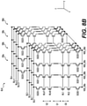
- FIG. 6A is a perspective view of a set of blocks in an example three-dimensional configuration of the memory array of FIG. 1 ;
- FIG. 6B depicts an example cross-sectional view of a portion of one of the blocks of FIG. 6A according to aspects of the disclosure
- FIG. 6C depicts a plot of memory hole diameter in the stack of FIG. 6B according to aspects of the disclosure
- FIG. 6D depicts a close-up view of the region 622 of the stack of FIG. 6B according to aspects of the disclosure
- FIG. 7A depicts a top view of an example word line layer WLL0 of the stack of FIG. 6B according to aspects of the disclosure
- FIG. 7B depicts a top view of an example top dielectric layer DL19 of the stack of FIG. 6B according to aspects of the disclosure
- FIG. 8A depicts example NAND strings in the sub-blocks SBa-SBd of FIG. 7A according to aspects of the disclosure
- FIG. 8B depicts another example view of NAND strings in sub-blocks according to aspects of the disclosure.
- FIG. 9 depicts a waveform of an example programming operation according to aspects of the disclosure n;
- FIGS. 10A and 10B depicts Vth distributions of memory cells after a first programming stage and a second stage of an example two-stage programming operation with four data states according to aspects of the disclosure
- FIG. 11 shows a default first programming stage, a proposed first programming stage leaving a fraction of cells below a first stage verify level, and a default threshold voltage distribution after the default first programming stage and a second programming stage, a proposed threshold distribution after the proposed first programming stage and the second programming stage according to aspects of the disclosure;
- FIG. 12 shows the first programming stage being stopped after the number of cells passing the first stage verify level is higher than the bit ignore number according to aspects of the disclosure
- FIG. 13 shows two experiments conducted to determine the impact of reduction of program verify loops by the apparatus according to aspects of the disclosure
- FIGS. 14A and 14B show threshold voltage distributions for a default condition (no program verify reduction) and reduced program verify condition for both experiments of FIG. 13 according to aspects of the disclosure;
- FIGS. 15A and 15B show that the final threshold voltage distribution width after second programming stage is degraded more for upper states as compared to lower states in the experiments of FIG. 13 when a lower tail is left behind according to aspects of the disclosure.
- FIGS. 16 and 17A-17C show steps of a method of operating the memory apparatus according to aspects of the disclosure.
- the present disclosure relates to non-volatile memory apparatuses of the type well-suited for use in many applications.
- the non-volatile memory apparatus and associated methods of forming of this disclosure will be described in conjunction with one or more example embodiments.
- the specific example embodiments disclosed are merely provided to describe the inventive concepts, features, advantages and objectives with sufficient clarity to permit those skilled in this art to understand and practice the disclosure.
- the example embodiments are provided so that this disclosure will be thorough, and will fully convey the scope to those who are skilled in the art. Numerous specific details are set forth such as examples of specific components, devices, and methods, to provide a thorough understanding of embodiments of the present disclosure.
- a programming operation for a set of memory cells typically involves applying a series of program voltages to the memory cells after the memory cells are provided in an erased state.
- Each program voltage is provided in a program loop, also referred to as a program-verify iteration.
- the program voltage may be applied to a word line which is connected to control gates of the memory cells.
- incremental step pulse programming is performed, where the program voltage is increased by a step size in each program loop. Verify operations may be performed after each program voltage to determine whether the memory cells have completed programming. When programming is completed for a memory cell, it can be locked out from further programming while programming continues for other memory cells in subsequent program loops.
- Each memory cell may be associated with a data state according to write data in a program command. Based on its data state, a memory cell will either remain in the erased state or be programmed to a data state (a programmed data state) different from the erased state.
- a memory cell will either remain in the erased state or be programmed to a data state (a programmed data state) different from the erased state.
- A, B and C data states see FIG. 10B
- In a four-bit per cell memory device there are sixteen data states including the erased state and fifteen higher data states referred to as the Er, 1, 2, 3, 4, 5, 6, 7, 8, 9, A, B, C, D, E and F data states.
- the write data is stored in latches associated with the memory cells.
- the latches of a memory cell can be read to determine the data state to which the cell is to be programmed.
- Each programmed data state is associated with a verify voltage such that a memory cell with a given data state is considered to have completed programming when a sensing operation determines its threshold voltage (Vth) is above the associated verify voltage.
- Vth threshold voltage
- a sensing operation can determine whether a memory cell has a Vth above the associated verify voltage by applying the associated verify voltage to the control gate and sensing a current through the memory cell. If the current is relatively high, this indicates the memory cell is in a conductive state, such that the Vth is less than the control gate voltage. If the current is relatively low, this indicates the memory cell is in a non-conductive state, such that the Vth is above the control gate voltage.
- the verify voltage which is used to determine that a memory cell has completed programming may be referred to as a final or lockout verify voltage.
- an additional verify voltage may be used to determine that a memory cell is close to completion of the programming.
- This additional verify voltage may be referred to as an offset verify voltage, and can be lower than the final verify voltage.
- the programming speed of the memory cell can be reduced such as by elevating a voltage of a respective bit line during one or more subsequent program voltages.
- a memory cell which is to be programmed to the A data state can be subject to verify tests at VvAf, an offset verify voltage of the A data state, and VvA, a final verify voltage of the A data state.
- a verify test involves applying a verification signal to the control gates of the selected memory cells via a selected word line, pre-charging sense circuits which are connected to the selected memory cells via respective bit lines and observing an amount of discharge in the sense circuits for a specified discharge period. Moreover, this is repeated for each verify voltage of the verification signal. Also, the time consumed will increase as the number of data states increases.
- two stage programming schemes may be used to tighten the threshold voltage distributions, compared to full sequence or one stage programming schemes.
- such two stage programming schemes can improve both neighbor word line interference (NWI) and short term data retention (STDR), resulting in tighter threshold voltage distributions.
- NWI neighbor word line interference
- STDR short term data retention
- two stage programming schemes can result in degraded performance compared to one stage programming schemes.
- FIG. 1A is a block diagram of an example memory device.
- the memory device or apparatus 100 may include one or more memory die 108 .
- the memory die 108 includes a memory structure 126 of memory cells, such as an array of memory cells, control circuitry 110 , and read/write circuits 128 .
- the memory structure 126 is addressable by word lines via a row decoder 124 and by bit lines via a column decoder 132 .
- the read/write circuits 128 include multiple sense blocks SB1, SB2, . . . , SBp (sensing circuitry) and allow a page of memory cells to be read or programmed in parallel.
- a controller 122 is included in the same memory device 100 (e.g., a removable storage card) as the one or more memory die 108 . Commands and data are transferred between the host 140 and controller 122 via a data bus 120 , and between the controller and the one or more memory die 108 via lines 118 .
- the memory structure can be 2D or 3D.
- the memory structure may comprise one or more array of memory cells including a 3D array.
- the memory structure may comprise a monolithic three dimensional memory structure in which multiple memory levels are formed above (and not in) a single substrate, such as a wafer, with no intervening substrates.
- the memory structure may comprise any type of non-volatile memory that is monolithically formed in one or more physical levels of arrays of memory cells having an active area disposed above a silicon substrate.
- the memory structure may be in a non-volatile memory device having circuitry associated with the operation of the memory cells, whether the associated circuitry is above or within the substrate.
- the control circuitry 110 cooperates with the read/write circuits 128 to perform memory operations on the memory structure 126 , and includes a state machine 112 , an on-chip address decoder 114 , and a power control module 116 .
- the state machine 112 provides chip-level control of memory operations.
- a storage region 113 may be provided, e.g., for verify parameters as described herein. These can be parameters related to a verify scheme.
- the on-chip address decoder 114 provides an address interface between that used by the host or a memory controller to the hardware address used by the decoders 124 and 132 .
- the power control module 116 controls the power and voltages supplied to the word lines and bit lines during memory operations. It can include drivers for word lines, SGS and SGD transistors and source lines.
- the sense blocks can include bit line drivers, in one approach.
- An SGS transistor is a select gate transistor at a source end of a NAND string
- an SGD transistor is a select gate transistor at a drain end of a NAND string.
- a control circuit may include any one of, or a combination of, control circuitry 110 , state machine 112 , decoders 114 / 132 , power control module 116 , sense blocks SBb, SB2, . . . , SBp, read/write circuits 128 , controller 122 , and so forth.
- the control circuits can include a programming circuit configured to perform a programming operation for one set of memory cells, wherein: the one set of memory cells comprises memory cells assigned to represent one data state among a plurality of data states and memory cells assigned to represent another data state among the plurality of data states; the programming operation comprising a plurality of program-verify iterations; and in each program-verify iteration, the programming circuit performs programming for the one word line after which the programming circuit applies a verification signal to the one word line.
- the control circuits can also include a counting circuit configured to obtain a count of memory cells which pass a verify test for the one data state.
- the control circuits can also include a determination circuit configured to determine, based on an amount by which the count exceeds a threshold, a particular program-verify iteration among the plurality of program-verify iterations in which to perform a verify test for the another data state for the memory cells assigned to represent the another data state.
- FIG. 1B is a block diagram of an example control circuit 150 which comprises a programming circuit 151 , a counting circuit 152 and a determination circuit 153 .
- the programming circuit may include software, firmware and/or hardware which implements, e.g., steps 1200 - 1240 of FIGS. 17 and 18A-18C .
- the counting circuit may include software, firmware and/or hardware which implements, e.g., step 1202 of FIG. 18B .
- the determination circuit may include software, firmware and/or hardware which implements, e.g., steps 1206 , 1218 , and 1236 of FIGS. 18A-18C .
- the off-chip controller 122 may comprise a processor 122 c , storage devices (memory) such as ROM 122 a and RAM 122 b and an error-correction code (ECC) engine 245 .
- the ECC engine can correct a number of read errors which are caused when the upper tail of a Vth distribution becomes too high. However, uncorrectable errors may exists in some cases. The techniques provided herein reduce the likelihood of uncorrectable errors.
- the storage device comprises code such as a set of instructions, and the processor is operable to execute the set of instructions to provide the functionality described herein.
- the processor can access code from a storage device 126 a of the memory structure, such as a reserved area of memory cells in one or more word lines.
- code can be used by the controller to access the memory structure such as for programming, read and erase operations.
- the code can include boot code and control code (e.g., set of instructions).
- the boot code is software that initializes the controller during a booting or startup process and enables the controller to access the memory structure.
- the code can be used by the controller to control one or more memory structures.
- the processor 122 c fetches the boot code from the ROM 122 a or storage device 126 a for execution, and the boot code initializes the system components and loads the control code into the RAM 122 b . Once the control code is loaded into the RAM, it is executed by the processor.
- the control code includes drivers to perform basic tasks such as controlling and allocating memory, prioritizing the processing of instructions, and controlling input and output ports.
- control code can include instructions to perform the functions described herein including the steps of the flowcharts discussed further below and provide the voltage waveforms including those discussed further below.
- the host is a computing device (e.g., laptop, desktop, smartphone, tablet, digital camera) that includes one or more processors, one or more processor readable storage devices (RAM, ROM, flash memory, hard disk drive, solid state memory) that store processor readable code (e.g., software) for programming the one or more processors to perform the methods described herein.
- the host may also include additional system memory, one or more input/output interfaces and/or one or more input/output devices in communication with the one or more processors.
- non-volatile memory in addition to NAND flash memory can also be used.
- Semiconductor memory devices include volatile memory devices, such as dynamic random access memory (“DRAM”) or static random access memory (“SRAM”) devices, non-volatile memory devices, such as resistive random access memory (“ReRAM”), electrically erasable programmable read only memory (“EEPROM”), flash memory (which can also be considered a subset of EEPROM), ferroelectric random access memory (“FRAM”), and magnetoresistive random access memory (“MRAM”), and other semiconductor elements capable of storing information.
- volatile memory devices such as dynamic random access memory (“DRAM”) or static random access memory (“SRAM”) devices
- non-volatile memory devices such as resistive random access memory (“ReRAM”), electrically erasable programmable read only memory (“EEPROM”), flash memory (which can also be considered a subset of EEPROM), ferroelectric random access memory (“FRAM”), and magnetoresistive random access memory (“MRAM”), and other semiconductor elements capable of storing information.
- ReRAM resistive random access memory
- EEPROM electrically erasable
- the memory devices can be formed from passive and/or active elements, in any combinations.
- passive semiconductor memory elements include ReRAM device elements, which in some embodiments include a resistivity switching storage element, such as an anti-fuse or phase change material, and optionally a steering element, such as a diode or transistor.
- active semiconductor memory elements include EEPROM and flash memory device elements, which in some embodiments include elements containing a charge storage region, such as a floating gate, conductive nanoparticles, or a charge storage dielectric material.
- NAND memory typically contain memory elements connected in series.
- a NAND string is an example of a set of series-connected transistors comprising memory cells and SG transistors.
- a NAND memory array may be configured so that the array is composed of multiple strings of memory in which a string is composed of multiple memory elements sharing a single bit line and accessed as a group.
- memory elements may be configured so that each element is individually accessible, e.g., a NOR memory array.
- NAND and NOR memory configurations are examples, and memory elements may be otherwise configured.
- the semiconductor memory elements located within and/or over a substrate may be arranged in two or three dimensions, such as a two dimensional memory structure or a three dimensional memory structure.
- the semiconductor memory elements are arranged in a single plane or a single memory device level.
- memory elements are arranged in a plane (e.g., in an x-y direction plane) which extends substantially parallel to a major surface of a substrate that supports the memory elements.
- the substrate may be a wafer over or in which the layer of the memory elements are formed or it may be a carrier substrate which is attached to the memory elements after they are formed.
- the substrate may include a semiconductor such as silicon.
- the memory elements may be arranged in the single memory device level in an ordered array, such as in a plurality of rows and/or columns. However, the memory elements may be arrayed in non-regular or non-orthogonal configurations.
- the memory elements may each have two or more electrodes or contact lines, such as bit lines and word lines.
- a three dimensional memory array is arranged so that memory elements occupy multiple planes or multiple memory device levels, thereby forming a structure in three dimensions (i.e., in the x, y and z directions, where the z direction is substantially perpendicular and the x and y directions are substantially parallel to the major surface of the substrate).
- a three dimensional memory structure may be vertically arranged as a stack of multiple two dimensional memory device levels.
- a three dimensional memory array may be arranged as multiple vertical columns (e.g., columns extending substantially perpendicular to the major surface of the substrate, i.e., in the y direction) with each column having multiple memory elements.
- the columns may be arranged in a two dimensional configuration, e.g., in an x-y plane, resulting in a three dimensional arrangement of memory elements with elements on multiple vertically stacked memory planes.
- Other configurations of memory elements in three dimensions can also constitute a three dimensional memory array.
- the memory elements may be coupled together to form a NAND string within a single horizontal (e.g., x-y) memory device level.
- the memory elements may be coupled together to form a vertical NAND string that traverses across multiple horizontal memory device levels.
- Other three dimensional configurations can be envisioned wherein some NAND strings contain memory elements in a single memory level while other strings contain memory elements which span through multiple memory levels.
- Three dimensional memory arrays may also be designed in a NOR configuration and in a ReRAM configuration.
- a monolithic three dimensional memory array typically, one or more memory device levels are formed above a single substrate.
- the monolithic three dimensional memory array may also have one or more memory layers at least partially within the single substrate.
- the substrate may include a semiconductor such as silicon.
- the layers constituting each memory device level of the array are typically formed on the layers of the underlying memory device levels of the array.
- layers of adjacent memory device levels of a monolithic three dimensional memory array may be shared or have intervening layers between memory device levels.
- non-monolithic stacked memories can be constructed by forming memory levels on separate substrates and then stacking the memory levels atop each other. The substrates may be thinned or removed from the memory device levels before stacking, but as the memory device levels are initially formed over separate substrates, the resulting memory arrays are not monolithic three dimensional memory arrays. Further, multiple two dimensional memory arrays or three dimensional memory arrays (monolithic or non-monolithic) may be formed on separate chips and then packaged together to form a stacked-chip memory device.
- Associated circuitry is typically required for operation of the memory elements and for communication with the memory elements.
- memory devices may have circuitry used for controlling and driving memory elements to accomplish functions such as programming and reading.
- This associated circuitry may be on the same substrate as the memory elements and/or on a separate substrate.
- a controller for memory read-write operations may be located on a separate controller chip and/or on the same substrate as the memory elements.
- FIG. 2 depicts blocks of memory cells in an example two-dimensional configuration of the memory array 126 of FIG. 1 .
- the memory array can include many blocks.
- Each example block 200 , 210 includes a number of NAND strings and respective bit lines, e.g., BL0, BL1, . . . which are shared among the blocks.
- Each NAND string is connected at one end to a drain select gate (SGD), and the control gates of the drain select gates are connected via a common SGD line.
- the NAND strings are connected at their other end to a source select gate which, in turn, is connected to a common source line 220 .
- Sixteen word lines, for example, WL0-WL15 extend between the source select gates and the drain select gates.
- dummy word lines which contain no user data, can also be used in the memory array adjacent to the select gate transistors. Such dummy word lines can shield the edge data word line from certain edge effects.
- non-volatile memory which may be provided in the memory array is a floating gate memory. See FIGS. 3A and 3B .
- Other types of non-volatile memory can also be used.
- a charge-trapping memory cell uses a non-conductive dielectric material in place of a conductive floating gate to store charge in a non-volatile manner. See FIGS. 4A and 4B .
- a triple layer dielectric formed of silicon oxide, silicon nitride and silicon oxide (“ONO”) is sandwiched between a conductive control gate and a surface of a semi-conductive substrate above the memory cell channel. The cell is programmed by injecting electrons from the cell channel into the nitride, where they are trapped and stored in a limited region.
- This stored charge then changes the threshold voltage of a portion of the channel of the cell in a manner that is detectable.
- the cell is erased by injecting hot holes into the nitride.
- a similar cell can be provided in a split-gate configuration where a doped polysilicon gate extends over a portion of the memory cell channel to form a separate select transistor.
- NROM cells are used. Two bits, for example, are stored in each NROM cell, where an ONO dielectric layer extends across the channel between source and drain diffusions. The charge for one data bit is localized in the dielectric layer adjacent to the drain, and the charge for the other data bit localized in the dielectric layer adjacent to the source. Multi-state data storage is obtained by separately reading binary states of the spatially separated charge storage regions within the dielectric. Other types of non-volatile memory are also known.
- FIG. 3A depicts a cross-sectional view of example floating gate memory cells in NAND strings.
- a bit line or NAND string direction goes into the page, and a word line direction goes from left to right.
- word line 324 extends across NAND strings which include respective channel regions 306 , 316 and 326 .
- the memory cell 300 includes a control gate 302 , a floating gate 304 , a tunnel oxide layer 305 and the channel region 306 .
- the memory cell 310 includes a control gate 312 , a floating gate 314 , a tunnel oxide layer 315 and the channel region 316 .
- the memory cell 320 includes a control gate 322 , a floating gate 321 , a tunnel oxide layer 325 and the channel region 326 .
- Each memory cell is in a different respective NAND string.
- An inter-poly dielectric (IPD) layer 328 is also depicted.
- the control gates are portions of the word line.
- control gate wraps around the floating gate, increasing the surface contact area between the control gate and floating gate. This results in higher IPD capacitance, leading to a higher coupling ratio which makes programming and erase easier.
- the spacing between neighboring cells becomes smaller so there is almost no space for the control gate and the IPD between two adjacent floating gates.
- the flat or planar memory cell has been developed in which the control gate is flat or planar; that is, it does not wrap around the floating gate, and its only contact with the charge storage layer is from above it. In this case, there is no advantage in having a tall floating gate. Instead, the floating gate is made much thinner. Further, the floating gate can be used to store charge, or a thin charge trap layer can be used to trap charge. This approach can avoid the issue of ballistic electron transport, where an electron can travel through the floating gate after tunneling through the tunnel oxide during programming.
- FIG. 3B depicts a cross-sectional view of the structure of FIG. 3A along line 329 .
- the NAND string 330 includes an SGS transistor 331 , example memory cells 300 , 333 , . . . , 334 and 335 , and an SGD transistor 336 .
- the memory cell 300 includes the control gate 302 , the IPD layer 328 , the floating gate 304 and the tunnel oxide layer 305 , consistent with FIG. 3A . Passageways in the IPD layer in the SGS and SGD transistors allow the control gate layers and floating gate layers to communicate.
- the control gate and floating gate layers may be polysilicon and the tunnel oxide layer may be silicon oxide, for instance.
- the IPD layer can be a stack of nitrides (N) and oxides (O) such as in a N—O—N—O—N configuration.
- the NAND string may be formed on a substrate which comprises a p-type substrate region 355 , an n-type well 356 and a p-type well 357 .
- N-type source/drain diffusion regions sd1, sd2, sd3, sd4, sd5, sd6 and sd7 are formed in the p-type well.
- a channel voltage, Vch may be applied directly to the channel region of the substrate.
- FIG. 4A depicts a cross-sectional view of example charge-trapping memory cells in NAND strings.
- the view is in a word line direction of memory cells comprising a flat control gate and charge-trapping regions as a 2D example of memory cells in the memory cell array 126 of FIG. 1 .
- Charge-trapping memory can be used in NOR and NAND flash memory device. This technology uses an insulator such as an SiN film to store electrons, in contrast to a floating-gate MOSFET technology which uses a conductor such as doped polycrystalline silicon to store electrons.
- a word line (WL) 424 extends across NAND strings which include respective channel regions 406 , 416 and 426 .
- Portions of the word line provide control gates 402 , 412 and 422 .
- IPD layer 428 Below the word line is an IPD layer 428 , charge-trapping layers 404 , 414 and 421 , polysilicon layers 405 , 415 and 425 and tunneling layer layers 409 , 407 and 408 .
- Each charge-trapping layer extends continuously in a respective NAND string.
- a memory cell 400 includes the control gate 402 , the charge-trapping layer 404 , the polysilicon layer 405 and a portion of the channel region 406 .
- a memory cell 410 includes the control gate 412 , the charge-trapping layer 414 , a polysilicon layer 415 and a portion of the channel region 416 .
- a memory cell 420 includes the control gate 422 , the charge-trapping layer 421 , the polysilicon layer 425 and a portion of the channel region 426 .
- a flat control gate is used here instead of a control gate that wraps around a floating gate.
- One advantage is that the charge-trapping layer can be made thinner than a floating gate. Additionally, the memory cells can be placed closer together.
- FIG. 4B depicts a cross-sectional view of the structure of FIG. 4A along line 429 .
- the view shows a NAND string 430 having a flat control gate and a charge-trapping layer.
- the NAND string 430 includes an SGS transistor 431 , example memory cells 400 , 433 , . . . , 434 and 435 , and an SGD transistor 435 .
- the NAND string may be formed on a substrate which comprises a p-type substrate region 455 , an n-type well 456 and a p-type well 457 .
- N-type source/drain diffusion regions sd1, sd2, sd3, sd4, sd5, sd6 and sd7 are formed in the p-type well 457 .
- a channel voltage, Vch may be applied directly to the channel region of the substrate.
- the memory cell 400 includes the control gate 402 and the IPD layer 428 above the charge-trapping layer 404 , the polysilicon layer 405 , the tunneling layer 409 and the channel region 406 .
- the control gate layer may be polysilicon and the tunneling layer may be silicon oxide, for instance.
- the IPD layer can be a stack of high-k dielectrics such as AlOx or HfOx which help increase the coupling ratio between the control gate layer and the charge-trapping or charge storing layer.
- the charge-trapping layer can be a mix of silicon nitride and oxide, for instance.
- the SGD and SGS transistors have the same configuration as the memory cells but with a longer channel length to ensure that current is cutoff in an inhibited NAND string.
- the layers 404 , 405 and 409 extend continuously in the NAND string.
- portions of the layers 404 , 405 and 409 which are between the control gates 402 , 412 and 422 can be removed, exposing a top surface of the channel 406 .
- FIG. 5A depicts an example block diagram of the sense block SB1 of FIG. 1 .
- a sense block comprises multiple sense circuits. Each sense circuit is associated with data latches.
- the example sense circuits 550 a , 551 a , 552 a and 553 a are associated with the data latches 550 b , 551 b , 552 b and 553 b , respectively.
- different subsets of bit lines can be sensed using different respective sense blocks. This allows the processing load which is associated with the sense circuits to be divided up and handled by a respective processor in each sense block.
- a sense circuit controller 560 in SB1 can communicate with the set of sense circuits and latches.
- the sense circuit controller may include a pre-charge circuit 561 which provides a voltage to each sense circuit for setting a pre-charge voltage.
- the voltage is provided to each sense circuit independently, e.g., via the data base 503 and a local bus such as LBUS1 or LBUS2 in FIG. 5B .
- a common voltage is provided to each sense circuit concurrently, e.g., via the line 505 in FIG. 5B .
- the sense circuit controller may also include a memory 562 and a processor 563 .
- the memory 562 may store code which is executable by the processor to perform the functions described herein.
- These functions can include reading latches which are associated with the sense circuits, setting bit values in the latches and providing voltages for setting pre-charge levels in sense nodes of the sense circuits. Further example details of the sense circuit controller and the sense circuits 550 a and 551 a are provided below.
- FIG. 5B depicts another example block diagram of the sense block SB1 of FIG. 1 .
- the sense circuit controller 560 communicates with multiple sense circuits including example sense circuits 550 a and 551 a , also shown in FIG. 5A .
- the sense circuit 550 a includes latches 550 b , including a trip latch 526 , an offset verify latch 527 and data state latches 528 .
- the sense circuit further includes a voltage clamp 521 such as a transistor which sets a pre-charge voltage at a sense node 522 .
- a sense node to bit line (BL) switch 523 selectively allows the sense node to communicate with a bit line 525 , e.g., the sense node is electrically connected to the bit line so that the sense node voltage can decay.
- the bit line 525 is connected to one or more memory cells such as a memory cell MC1.
- a voltage clamp 524 can set a voltage on the bit line, such as during a sensing operation or during a program voltage.
- a local bus, LBUS1 allows the sense circuit controller to communicate with components in the sense circuit, such as the latches 550 b and the voltage clamp in some cases.
- the sense circuit controller To communicate with the sense circuit 550 a , the sense circuit controller provides a voltage via a line 502 to a transistor 504 to connect LBUS1 with a data bus DBUS, 503 .
- the communicating can include sending data to the sense circuit and/or receive data from the sense circuit.
- the sense circuit controller can communicate with different sense circuits in a time-multiplexed manner, for instance.
- a line 505 may be connected to the voltage clamp in each sense circuit, in one approach.
- the sense circuit 551 a includes latches 551 b , including a trip latch 546 , an offset verify latch 547 and data state latches 548 .
- a voltage clamp 541 may be used to set a pre-charge voltage at a sense node 542 .
- a sense node to bit line (BL) switch 543 selectively allows the sense node to communicate with a bit line 545 , and a voltage clamp 544 can set a voltage on the bit line.
- the bit line 545 is connected to one or more memory cells such as a memory cell MC2.
- a local bus, LBUS2 allows the sense circuit controller to communicate with components in the sense circuit, such as the latches 551 b and the voltage clamp in some cases.
- the sense circuit controller provides a voltage via a line 501 to a transistor 506 to connect LBUS2 with DBUS.
- the sense circuit 550 a may be a first sense circuit which comprises a first trip latch 526 and the sense circuit 551 a may be a second sense circuit which comprises a second trip latch 546 .
- the sense circuit 550 a is an example of a first sense circuit comprising a first sense node 522 , where the first sense circuit is associated with a first memory cell MC1 and a first bit line 525 .
- the sense circuit 551 a is an example of a second sense circuit comprising a second sense node 542 , where the second sense circuit is associated with a second memory cell MC2 and a second bit line 545 .
- FIG. 6A is a perspective view of a set of blocks 600 in an example three-dimensional configuration of the memory array 126 of FIG. 1 .
- the circuitry can include voltage drivers 605 which can be connected to control gate layers of the blocks. In one approach, control gate layers at a common height in the blocks are commonly driven.
- the substrate 601 can also carry circuitry under the blocks, along with one or more lower metal layers which are patterned in conductive paths to carry signals of the circuitry.
- the blocks are formed in an intermediate region 602 of the memory device.
- each block comprises a stacked area of memory cells, where alternating levels of the stack represent word lines.
- each block has opposing tiered sides from which vertical contacts extend upward to an upper metal layer to form connections to conductive paths. While four blocks are depicted as an example, two or more blocks can be used, extending in the x- and/or y-directions.
- the length of the plane, in the x-direction represents a direction in which signal paths to word lines extend in the one or more upper metal layers (a word line or SGD line direction)
- the width of the plane, in the y-direction represents a direction in which signal paths to bit lines extend in the one or more upper metal layers (a bit line direction).
- the z-direction represents a height of the memory device.
- FIG. 6B depicts an example cross-sectional view of a portion of one of the blocks of FIG. 6A .
- the block comprises a stack 610 of alternating conductive and dielectric layers.
- the conductive layers comprise two SGD layers, two SGS layers and four dummy word line layers DWLD0, DWLD1, DWLS0 and DWLS1, in addition to data word line layers (word lines) WLL0-WLL10.
- the dielectric layers are labelled as DL0-DL19.
- regions of the stack which comprise NAND strings NS1 and NS2 are depicted. Each NAND string encompasses a memory hole 618 or 619 which is filled with materials which form memory cells adjacent to the word lines.
- a region 622 of the stack is shown in greater detail in FIG. 6D .
- the stack includes a substrate 611 , an insulating film 612 on the substrate, and a portion of a source line SL.
- NS1 has a source-end 613 at a bottom 614 of the stack and a drain-end 615 at a top 616 of the stack.
- Metal-filled slits 617 and 620 may be provided periodically across the stack as interconnects which extend through the stack, such as to connect the source line to a line above the stack. The slits may be used during the formation of the word lines and subsequently filled with metal.
- a portion of a bit line BL0 is also depicted.
- a conductive via 621 connects the drain-end 615 to BL0.
- FIG. 6C depicts a plot of memory hole diameter in the stack of FIG. 6B .
- the vertical axis is aligned with the stack of FIG. 6B and depicts a width (wMH), e.g., diameter, of the memory holes 618 and 619 .
- the word line layers WLL0-WLL10 of FIG. 6A are repeated as an example and are at respective heights z0-z10 in the stack.
- the memory holes which are etched through the stack have a very high aspect ratio. For example, a depth-to-diameter ratio of about 25-30 is common.
- the memory holes may have a circular cross-section. Due to the etching process, the memory hole width can vary along the length of the hole.
- the diameter becomes progressively smaller from the top to the bottom of the memory hole. That is, the memory holes are tapered, narrowing at the bottom of the stack. In some cases, a slight narrowing occurs at the top of the hole near the select gate so that the diameter becomes slight wider before becoming progressively smaller from the top to the bottom of the memory hole.
- the programming speed including the program slope and erase speed of the memory cells can vary based on their position along the memory hole, e.g., based on their height in the stack. With a smaller diameter memory hole, the electric field across the tunnel oxide is relatively stronger, so that the programming and erase speed is relatively higher.
- One approach is to define groups of adjacent word lines for which the memory hole diameter is similar, e.g., within a defined range of diameter, and to apply a verify scheme for each word line in a group. Different groups can have different verify schemes. For example, groups G0, G1 and G2 include WLL0-WLL2, WLL3-WLL6 and WLL7-WLL10, respectively.
- FIG. 6D depicts a close-up view of the region 622 of the stack of FIG. 6B .
- Memory cells are formed at the different levels of the stack at the intersection of a word line layer and a memory hole.
- SGD transistors 680 and 681 are provided above dummy memory cells 682 and 683 and a data memory cell MC.
- a number of layers can be deposited along the sidewall (SW) of the memory hole 630 and/or within each word line layer, e.g., using atomic layer deposition.
- each column (e.g., the pillar which is formed by the materials within a memory hole) can include a charge-trapping layer or film 663 such as SiN or other nitride, a tunneling layer 664 , a polysilicon body or channel 665 , and a dielectric core 666 .
- a word line layer can include a blocking oxide/block high-k material 660 , a metal barrier 661 , and a conductive metal 662 such as Tungsten as a control gate.
- control gates 690 , 691 , 692 , 693 and 694 are provided. In this example, all of the layers except the metal are provided in the memory hole. In other approaches, some of the layers can be in the control gate layer. Additional pillars are similarly formed in the different memory holes.
- a pillar can form a columnar active area (AA) of a NAND string.
- Each of the memory holes can be filled with a plurality of annular layers comprising a blocking oxide layer, a charge trapping layer, a tunneling layer and a channel layer.
- a core region of each of the memory holes is filled with a body material, and the plurality of annular layers are between the core region and the word line in each of the memory holes.
- the NAND string can be considered to have a floating body channel because the length of the channel is not formed on a substrate. Further, the NAND string is provided by a plurality of word line layers above one another in a stack, and separated from one another by dielectric layers.
- FIG. 7A depicts a top view of an example word line layer WLL0 of the stack of FIG. 6B .
- a 3D memory device can comprise a stack of alternating conductive and dielectric layers.
- the conductive layers provide the control gates of the SG transistors and memory cells.
- the layers used for the SG transistors are SG layers and the layers used for the memory cells are word line layers.
- memory holes are formed in the stack and filled with a charge-trapping material and a channel material.
- Source lines are connected to the NAND strings below the stack and bit lines are connected to the NAND strings above the stack.
- a block BLK in a 3D memory device can be divided into sub-blocks, where each sub-block comprises a set of NAND string which have a common SGD control line. For example, see the SGD lines/control gates SGD0, SGD1, SGD2 and SGD3 in the sub-blocks SBa, SBb, SBc and SBd, respectively.
- a word line layer in a block can be divided into regions. Each region is in a respective sub-block are can extend between slits which are formed periodically in the stack to process the word line layers during the fabrication process of the memory device. This processing can include replacing a sacrificial material of the word line layers with metal.
- the distance between slits should be relatively small to account for a limit in the distance that an etchant can travel laterally to remove the sacrificial material, and that the metal can travel to fill a void which is created by the removal of the sacrificial material.
- the distance between slits may allow for a few rows of memory holes between adjacent slits.
- the layout of the memory holes and slits should also account for a limit in the number of bit lines which can extend across the region while each bit line is connected to a different memory cell. After processing the word line layers, the slits can optionally be filed with metal to provide an interconnect through the stack.
- a row here is a group of memory holes which are aligned in the x-direction. Moreover, the rows of memory holes are in a staggered pattern to increase the density of the memory holes.
- the word line layer or word line is divided into regions WLL0a, WLL0b, WLL0c and WLL0d which are each connected by a connector 713 .
- the last region of a word line layer in a block can be connected to a first region of a word line layer in a next block, in one approach.
- the connector is connected to a voltage driver for the word line layer.
- the region WLL0a has example memory holes 710 and 711 along a line 712 .
- the region WLL0b has example memory holes 714 and 715 .
- the region WLL0c has example memory holes 716 and 717 .
- the region WLL0d has example memory holes 718 and 719 .
- the memory holes are also shown in FIG. 7B .
- Each memory hole can be part of a respective NAND string.
- the memory holes 710 , 714 , 716 and 718 can be part of NAND strings NS0_SBa, NS0_SBb, NS0_SBc and NS0_SBd, respectively.
- Each circle represents the cross-section of a memory hole at a word line layer or SG layer.
- Example circles shown with dashed lines represent memory cells which are provided by the materials in the memory hole and by the adjacent word line layer.
- memory cells 720 and 721 are in WLL0a
- memory cells 724 and 725 are in WLL0b
- memory cells 726 and 727 are in WLL0c
- memory cells 728 and 729 are in WLL0d. These memory cells are at a common height in the stack.
- Metal-filled slits 701 , 702 , 703 and 704 may be located between and adjacent to the edges of the regions WLL0a-WLL0d.
- the metal-filled slits provide a conductive path from the bottom of the stack to the top of the stack.
- a source line at the bottom of the stack may be connected to a conductive line above the stack, where the conductive line is connected to a voltage driver in a peripheral region of the memory device. See also FIG. 8A for further details of the sub-blocks SBa-SBd of FIG. 7A .
- FIG. 7B depicts a top view of an example top dielectric layer DL19 of the stack of FIG. 6B .
- the dielectric layer is divided into regions DL19 a, DL19 b, DL19 c and DL19 d.
- Each region can be connected to a respective voltage driver. This allows a set of memory cells in one region of a word line layer to be programmed concurrently, with each memory cell being in a respective NAND string which is connected to a respective bit line.
- a voltage can be set on each bit line to allow or inhibit programming during each program voltage.
- the region DL19a has the example memory holes 710 and 711 along a line 712 a which is coincident with a bit line BL0.
- a number of bit lines extend above the memory holes and are connected to the memory holes as indicated by the “X” symbols.
- BL0 is connected to a set of memory holes which includes the memory holes 711 , 715 , 717 and 719 .
- Another example bit line BL1 is connected to a set of memory holes which includes the memory holes 710 , 714 , 716 and 718 .
- the metal-filled slits 701 , 702 , 703 and 704 from FIG. 7A are also depicted, as they extend vertically through the stack.
- the bit lines can be numbered in a sequence BL0-BL23 across the DL19 layer in the ⁇ x direction.
- bit lines are connected to cells in different rows.
- BL0, BL4, BL8, BL12, BL16 and BL20 are connected to cells in a first row of cells at the right hand edge of each region.
- BL2, BL6, BL10, BL14, BL18 and BL22 are connected to cells in an adjacent row of cells, adjacent to the first row at the right hand edge.
- BL3, BL7, BL11, BL15, BL19 and BL23 are connected to cells in a first row of cells at the left hand edge of each region.
- BL1, BL5, BL9, BL13, BL17 and BL21 are connected to cells in an adjacent row of cells, adjacent to the first row at the left hand edge.
- FIG. 8A depicts example NAND strings in the sub-blocks SBa-SBd of FIG. 7A .
- the sub-blocks are consistent with the structure of FIG. 6B .
- the conductive layers in the stack are depicted for reference at the left hand side.
- Each sub-block includes multiple NAND strings, where one example NAND string is depicted.
- SBa comprises an example NAND string NS0_SBa
- SBb comprises an example NAND string NS0_SBb
- SBc comprises an example NAND string NS0_SBc
- SBd comprises an example NAND string NS0_SBd.
- NS0_SBa include SGS transistors 800 and 801 , dummy memory cells 802 and 803 , data memory cells 804 , 805 , 806 , 807 , 808 , 809 , 810 , 811 , 812 , 813 and 814 , dummy memory cells 815 and 816 , and SGD transistors 817 and 818 .
- NS0_SBb include SGS transistors 820 and 821 , dummy memory cells 822 and 823 , data memory cells 824 , 825 , 826 , 827 , 828 , 829 , 830 , 831 , 832 , 833 and 834 , dummy memory cells 835 and 836 , and SGD transistors 837 and 838 .
- NS0_SBc include SGS transistors 840 and 841 , dummy memory cells 842 and 843 , data memory cells 844 , 845 , 846 , 847 , 848 , 849 , 850 , 851 , 852 , 853 and 854 , dummy memory cells 855 and 856 , and SGD transistors 857 and 858 .
- NS0_SBd include SGS transistors 860 and 861 , dummy memory cells 862 and 863 , data memory cells 864 , 865 , 866 , 867 , 868 , 869 , 870 , 871 , 872 , 873 and 874 , dummy memory cells 875 and 876 , and SGD transistors 877 and 878 .
- a set of memory cells in each sub-block are at a common height.
- one set of memory cells (including the memory cell 804 ) is among a plurality of memory cells formed along tapered memory holes in a stack of alternating conductive and dielectric layers.
- the one set of memory cells is at a particular height z0 in the stack.
- Another set of memory cells (including the memory cell 824 ) connected to the one word line (WLL0) are also at the particular height.
- the another set of memory cells e.g., including the memory cell 812
- another word line e.g., WLL8 are at another height (z8) in the stack.
- FIG. 8B depicts another example view of NAND strings in sub-blocks.
- the NAND strings includes NS0_SBa, NS0_SBb, NS0_SBc and NS0_SBd, which have 48 word lines, WL0-WL47, in this example.
- Each sub-block comprises a set of NAND strings which extend in the x direction and which have a common SGD line, e.g., SGD0, SGD1, SGD2 or SGD3.
- SGD0, SGD1, SGD2 or SGD3 common SGD line
- the NAND strings NS0_SBa, NS0_SBb, NS0_SBc and NS0_SBd are in sub-blocks SBa, SBb, SBc and SBd, respectively. Further, example, groups of word lines G0, G1 and G2 are depicted.
- FIG. 9 depicts a waveform of an example programming operation.
- the horizontal axis depicts a program loop number and the vertical axis depicts control gate or word line voltage.
- a programming operation can involve applying a pulse train to a selected word line, where the pulse train includes multiple program loops or program-verify (PV) iterations.
- the program portion of the program-verify iteration comprises a program voltage
- the verify portion of the program-verify iteration comprises one or more verify voltages.
- ISPP Incremental Step Pulse Programming
- a pulse train typically includes program voltages which increase stepwise in amplitude in each program-verify iteration using a fixed of varying step size.
- a new pulse train can be applied in each programming stage of a multi-stage programming operation, starting at an initial Vpgm level and ending at a final Vpgm level which does not exceed a maximum allowed level.
- the initial Vpgm levels can be the same or different in different programming stages.
- the final Vpgm levels can also be the same or different in different programming stages.
- the step size can be the same or different in the different programming stages. In some cases, a smaller step size is used in a final programming stage to reduce Vth distribution widths.
- the pulse train 900 includes a series of program voltages 901 , 902 , 903 , 904 , 905 , 906 , 907 , 908 , 909 , 910 , 911 , 912 , 913 , 914 and 915 that are applied to a word line selected for programming, and an associated set of non-volatile memory cells.
- One, two or three verify voltages are provided after each program voltage as an example, based on the target data states which are being verified. 0 V may be applied to the selected word line between the program and verify voltages.
- an A-state verify voltage of VvA (e.g., waveform or programming signal 916 ) may be applied after each of the first, second and third program voltages 901 , 902 and 903 , respectively.
- A- and B-state verify voltages of VvA and VvB (e.g., programming signal 917 ) may be applied after each of the fourth, fifth and sixth program voltages 904 , 905 and 906 , respectively.
- A-, B- and C-state verify voltages of VvA, VvB and VvC (e.g., programming signal 918 ) may be applied after each of the seventh and eighth program voltages 907 and 908 , respectively.
- VvB and VvC may be applied after each of the ninth, tenth and eleventh program voltages 909 , 910 and 911 , respectively.
- a C-state verify voltage of VvC e.g., programming signal 1020
- FIGS. 10A and 10B show threshold voltage (Vth) distributions of memory cells in an example two-stage programming operation. Specifically, the memory cells are initially in the erased state (bits 11) as represented by the Vth distribution 1100 shown in FIG. 10A .
- FIG. 10B depicts Vth distributions of memory cells after a first programming stage and a second programming stage of the example two-stage programming operation with four data states. While two programming stages and four data states are shown, it should be appreciated that any number of programming stages may be utilized (e.g., three or four programming stages) and any number of data states are contemplated.
- the first programming stage causes the Vth of the A, B and C state cells to reach the Vth distributions 1002 a , 1004 a and 1006 a , using first verify voltages of VvAf, VvBf and VvCf, respectively.
- This first programming stage can be a rough programming which uses a relatively large step size, for instance, so that the Vth distributions 1002 a , 1004 a and 1006 a are relatively wide.
- the second programming stage may use a smaller step size and causes the Vth distributions 1002 a , 1004 a and 1006 a to transition to the final Vth distributions 1002 , 1004 and 1006 (e.g., narrower than Vth distributions 1002 a , 1004 a and 1006 a ), using second verify voltages of VvA, VvB, and VvC, respectively.
- This two-stage programming operation can achieve relatively narrow Vth distributions.
- a small number of A, B and C state cells (e.g., smaller than a predetermined number of the plurality of memory cells) may have a Vth which is below VvA, VvB or VvC, respectively, due to a bit ignore criteria.
- the apparatus e.g., memory device 100
- the control circuit e.g., control circuit 150
- the control circuit configured to perform a first programming stage including iteratively programming each of the plurality of memory cells (e.g., data memory cells 804 , 805 , 806 , 807 , 808 , 809 , 810 , 811 , 812 , 813 , 814 of FIG. 8A ) to one of a plurality of first program states (e.g., Vth distributions 1002 a , 10048 , and 1006 a of FIG. 10B ).
- Vth distributions 1002 a , 10048 , and 1006 a of FIG. 10B
- the first programming stage also includes verifying that one or more of the plurality of memory cells has a threshold voltage above one of a plurality of first verify voltages (e.g., verify voltages VvAf, VvBf, VvCf of FIG. 10B ) corresponding to the plurality of first program states.
- a plurality of first verify voltages e.g., verify voltages VvAf, VvBf, VvCf of FIG. 10B
- all cells continue to receive program pulses until their threshold voltages are above a desired first stage verify level 1100 (as shown by 1102 on the left in FIG. 11 ).
- the control circuit instead of ending the first programming stage after all of the plurality of memory cells are verified to be above the one of a plurality of first verify voltages (e.g., the first stage verify level 1100 ), the control circuit ends the first programming stage before all of the plurality of memory cells are verified (as shown by 1104 on the right in FIG. 11 ).
- a fraction 1106 of the plurality of memory cells are left below the one of the plurality of first verify voltages during the first programming stage.
- the fraction 1106 of the plurality of memory cells below the one of the plurality of first verify voltages can, for example, be greater than one half of a total number of the plurality of memory cells. Nevertheless, it should be appreciated that the fraction 1106 can be any amount.
- the control circuit then is configured to perform a second programming stage including iteratively programming each of the plurality of memory cells to one of a plurality of second program states (e.g., Vth distributions 1002 , 1004 , and 1006 of FIG. 10B ) and verifying that at least a predetermined number of the plurality of memory cells each has the threshold voltage above one of a plurality of second verify voltages (e.g., verify voltages VvA, VvB, VvC of FIG. 10B ) corresponding to the plurality of second program states. Consequently, the fraction 1106 or leftover cells from the first programming stage are programmed during the second programming stage (i.e., has the threshold voltage above one of the plurality of second verify voltages).
- a plurality of second program states e.g., Vth distributions 1002 , 1004 , and 1006 of FIG. 10B
- verify voltages VvA, VvB, VvC of FIG. 10B verify voltages VvA, VvB, Vv
- a default threshold voltage distribution 1108 i.e., after the first programming stage 1102 and the second programming stage
- a proposed threshold distribution 1110 i.e., after the first programming stage 1104 and the second programming stage
- a first stage verify level 1112 one of the plurality of second verify voltages
- control circuit is further configured to count a quantity of the one or more of the plurality memory cells having the threshold voltage above the one of the plurality of first verify voltages, such as first stage verify level 1100 (e.g., using the counting circuit 152 ).
- the control circuit continues programming and verifying and counting until the quantity is larger than a bit ignore number or threshold quantity P s .
- the first programming stage is stopped after the number of cells passing the verify level is higher than the bit ignore number, P s (region indicated by 1116 ), leaving a tail or fraction of non-programmed cells (region indicated by 1106 ).
- Another way to leave a tail or fraction 1106 of un-programmed bits would be to count lower-tail bits (i.e., those below the one of the plurality of first verify voltages). Yet, such an approach has some disadvantages. For example, if lower-tail bits (fraction 1106 ) are counted, the Bit Scan Pass Fail (BSPF) criterion would need to be significantly raised in order to appreciably reduce the number of verify pulses and hence improve performance. Higher BSPF requires larger circuit area (so counter circuits have enough bits) or longer scan timing, which results in increased cost and worse performance. Counting the upper tail or region 1116 more directly indicates when cells are first programmed to the required Vt.
- BSPF Bit Scan Pass Fail
- the plurality of memory cells of the apparatus are coupled to a plurality of word lines (e.g., word lines WLL0, Wll1, WLL2, WLL3, WLL4, WLL5, WLL6, WLL7, WLL8, WLL9, WLL10 of FIG. 8A ).
- the control circuit e.g., control circuit 150
- the control circuit is further configured to iteratively select one of the plurality of word lines and set a first programming voltage (e.g., starting with program voltage 901 of FIG. 9 ) for the first programming stage.
- the control circuit then applies the first programming voltage to the one of the plurality of word lines that is selected.
- the control circuit is configured to select a first verification signal (e.g., starting with verify voltage 916 of FIG.
- control circuit sets a first lockout status for each of the plurality of memory cells determined to have the threshold voltage above the one of the plurality of first verify voltages for the one of the plurality of first program states.
- control circuit is configured to increase the programming voltage (e.g., to another program voltage other than program voltage 901 of FIG. 9 ) and return to apply the first programming voltage to the one of the plurality of word lines that is selected.
- the control circuit determines whether there is another of the plurality of word lines to be programmed.
- the control circuit is configured to return to select one of the plurality of word lines and set the first programming voltage for the first programming stage in response to determining there is another of the plurality of word lines to be programmed.
- the control circuit ends the first programming stage before all of the plurality of memory cells are determined to have the threshold voltage above the one of the plurality of first verify voltages corresponding to the one the plurality of first program states for each of the plurality of memory cells.
- the control circuit is further configured to iteratively select one of the plurality of word lines and set a second programming voltage for the second programming stage.
- the control circuit is next configured to apply the second programming voltage to the one of the plurality of word lines that is selected.
- the control circuit selects a second verification signal for one of the plurality of second program states and apply the second verification signal to the one of the plurality of word lines that is selected while determining whether the threshold voltage for each of the plurality of memory cells connected to the one of the plurality of word lines is above the one of the plurality of second verify voltages for the one of the plurality of second program states.
- the control circuit is also configured to set a second lockout status for each of the plurality of memory cells determined to have the threshold voltage above the one of the plurality of second verify voltages for the one of the plurality of second program states.
- the control circuit increases the second programming voltage and returns to apply the second programming voltage to the one of the plurality of word lines that is selected.
- the control circuit is configured to determine whether there is another of the plurality of word lines to be programmed.
- the control circuit is configured to return to select one of the plurality of word lines and set the second programming voltage for the second programming stage in response to determining there is another of the plurality of word lines to be programmed.
- the control circuit ends the second programming stage once the predetermined number of the plurality of memory are determined to have the threshold voltage above the one of the plurality of second verify voltages corresponding to the one the plurality of second program states for each of the plurality of memory cells. While the predetermined number can, for example, be all of the plurality of memory cells, it should be understood that the predetermined number may instead be less than the total number of the plurality of memory cells.
- the measurement procedure includes the following steps: 1) first stage program only S2 with limited NLP and other states at erase, 2) first stage program S3 with limited NLP and other states at erase/inhibited, 3) first stage program S4 with limited NLP and other states at erase/inhibited, 4) first stage program S5-S15 without limited NLP and other states at erase/inhibited, and 5) second stage program 31-S15 with default options.
- states S2, S3 and S4 have been limited.
- states S2, S3, S4 need N, N+1, N+2 program loops, respectively to complete programming.
- the threshold voltage distributions for a default condition (no pvfy reduction) and reduced pvfy condition for both experiments are shown in FIGS. 14A and 14B .
- lower tails for S2-S4 can be seen for reduced pvfy mode.
- FIGS. 15A and 15B it is also observed in the experiments that the final Vt width after the second programming stage is degraded more for S4 ( FIG. 15B ) compared to S2 ( FIG. 15A ), when a lower tail is left behind for the two states. This indicates that a larger lower tail (e.g., fraction 1106 of FIG. 11 ) can be left behind for lower states compared to upper states.
- lower states could for example include Vth distribution 1002 and upper states could for example include Vth distributions 1004 and 1006 ; however, the example shown in FIG. 10B has four states rather than the experiments discussed herein.
- control circuit is further configured to determine the threshold quantity P s (region indicated as 1116 in FIG. 12 ) for each of the plurality of memory cells based on which of the plurality of second program states corresponds with each of the plurality of memory cells.
- the bit ignore BSPF, P s can be dependent on the state for any particular memory cell.
- the threshold voltage of each the plurality of memory cells is within a common range of threshold voltages (see for example FIG. 10B ). Therefore, the plurality of second program states includes one or more lower program states (e.g., Vth distribution 1002 of FIG. 10B ) having the threshold voltage that is closer to zero volts (i.e., closer to the erase state) and one or more upper program states (e.g., Vth distributions 1004 and 1006 of FIG. 10B ) having the threshold voltage that is further from zero volts than the one or more lower program states.
- Vth distribution 1002 of FIG. 10B the threshold voltage that is closer to zero volts (i.e., closer to the erase state)
- upper program states e.g., Vth distributions 1004 and 1006 of FIG. 10B
- the threshold quantity or bit ignore BSPF P s used for the one or more lower program states can be less than the threshold quantity used for the one or more upper program states (i.e., P S2 ⁇ P S3 ⁇ P S4 . . . ).
- a method of operating the memory apparatus including the plurality of memory cells is also provided.
- the method includes the step of 1200 performing a first programming stage including iteratively programming each of the plurality of memory cells to one of a plurality of first program states (e.g., Vth distributions 1002 a , 1004 a , and 1006 a of FIG.
- the fraction 1106 of the plurality of memory cells below the one of a plurality of first verify voltages can be greater than one half of a total number of the plurality of memory cells.
- the method can include the step of 1202 counting a quantity of the one or more of the plurality memory cells having the threshold voltage above the one of the plurality of first verify voltages such as first stage verify level 1100 of FIG. 11 (e.g., using the counting circuit 152 ).
- the method can also include the step of 1204 continuing programming and verifying and counting until the quantity is larger than a threshold quantity.
- the method can further include the step of 1206 determining the threshold quantity for each of the plurality of memory cells based on which of the plurality of second program states corresponds with each of the plurality of memory cells.
- the threshold voltage of each the plurality of memory cells can be within a common range of threshold voltages and the plurality of second program states includes one or more lower program states (e.g., Vth distribution 1002 of FIG. 10B ) having the threshold voltage being closer to zero volts and one or more upper program states (e.g., Vth distributions 1004 and 1006 of FIG. 10B ) having the threshold voltage being further from zero volts than the one or more lower program states. Therefore, the threshold quantity P s used for the one or more lower program states is less than the threshold quantity used for the one or more upper program states.
- the step of 1200 performing the first programming stage including iteratively programming each of the plurality of memory cells to one of the plurality of first program states and verifying that one or more of the plurality of memory cells has the threshold voltage, above one of the plurality of first verify voltages corresponding to the plurality of first program states and ending the first programming stage before all of the plurality of memory cells are verified thereby leaving the fraction of the plurality of memory cells below the one of the plurality of first verify voltages
- the method can continue by 1212 selecting a first verification signal for one of the plurality of first program states and applying the first verification signal to the one of the plurality of word lines that is selected while determining whether the threshold voltage for each of the plurality of memory cells connected to the one of the plurality of word lines is above the one of the plurality of first verify voltages for the one of the plurality of first program states.
- the next step of the method is 1214 setting a first lockout status for each of the plurality of memory cells determined to have the threshold voltage above the one of the plurality of first verify voltages for the one of the plurality of first program states.
- the method can then include the step of 1216 increasing the programming voltage and returning to applying the first programming voltage to the one of the plurality of word lines that is selected.
- the method proceeds with the step of 1220 returning to 1208 selecting one of the plurality of word lines and setting the first programming voltage for the first programming stage in response to determining there is another of the plurality of word lines to be programmed.
- the method then includes the step of 1222 ending the first programming stage before all of the plurality of memory cells are determined to have the threshold voltage above the one of the plurality of first verify voltages corresponding to the one the plurality of first program states for each of the plurality of memory cells.
- the method continues with the step of 1224 performing a second programming stage including iteratively programming each of the plurality of memory cells to one of a plurality of second program states (e.g., Vth distributions 1002 , 1004 , and 1006 of FIG. 10B ) and verifying that at least a predetermined number of the plurality of memory cells each has the threshold voltage above one of a plurality of second verify voltages (e.g., verify voltages VvA, VvB, VvC of FIG. 10B ) corresponding to the plurality of second program states.
- a plurality of second program states e.g., Vth distributions 1002 , 1004 , and 1006 of FIG. 10B
- verify voltages VvA, VvB, VvC of FIG. 10B verify voltages VvA, VvB, VvC of FIG. 10B
- the step of 1224 performing the second programming stage including iteratively programming each of the plurality of memory cells to one of the plurality of second program states and verifying that the at least a predetermined number of the plurality of memory cells each has the threshold voltage above one of the plurality of second verify voltages corresponding to the plurality of second program states can further include the step of 1226 selecting one of the plurality of word lines and set a second programming voltage for the second programming stage. The method can then include the step of 1228 applying the second programming voltage to the one of the plurality of word lines that is selected.
- step 1230 selecting a second verification signal for one of the plurality of second program states and applying the second verification signal to the one of the plurality of word lines that is selected while determining whether the threshold voltage for each of the plurality of memory cells connected to the one of the plurality of word lines is above the one of the plurality of second verify voltages for the one of the plurality of second program states.
- the method can then proceed with the step of 1232 setting a second lockout status for each of the plurality of memory cells determined to have the threshold voltage above the one of the plurality of second verify voltages for the one of the plurality of second program states.
- the method then includes the step of 1234 increasing the second programming voltage and returning to applying the second programming voltage to the one of the plurality of word lines that is selected.
- the next step of the method is 1236 determining whether there is another of the plurality of word lines to be programmed.
- the method continues with the step of 1238 returning to 1226 selecting one of the plurality of word lines and setting the second programming voltage for the second programming stage in response to determining there is another of the plurality of word lines to be programmed.
- the method can include the step of 1240 ending the second programming stage once the predetermined number of the plurality of memory are determined to have the threshold voltage above the one of the plurality of second verify voltages corresponding to the one the plurality of second program states for each of the plurality of memory cells.
- first, second, third, etc. may be used herein to describe various elements, components, regions, layers and/or sections, these elements, components, regions, layers and/or sections should not be limited by these terms. These terms may be only used to distinguish one element, component, region, layer or section from another region, layer or section. Terms such as “first,” “second,” and other numerical terms when used herein do not imply a sequence or order unless clearly indicated by the context. Thus, a first element, component, region, layer or section discussed below could be termed a second element, component, region, layer or section without departing from the teachings of the example embodiments.
- Spatially relative terms such as “inner,” “outer,” “beneath,” “below,” “lower,” “above,” “upper,” “top”, “bottom”, and the like, may be used herein for ease of description to describe one element's or feature's relationship to another element(s) or feature(s) as illustrated in the figures.
- Spatially relative terms may be intended to encompass different orientations of the device in use or operation in addition to the orientation depicted in the figures. For example, if the device in the figures is turned over, elements described as “below” or “beneath” other elements or features would then be oriented “above” the other elements or features.
- the example term “below” can encompass both an orientation of above and below.
- the device may be otherwise oriented (rotated 90 degrees or at other orientations) and the spatially relative descriptions used herein interpreted accordingly.
Landscapes
- Engineering & Computer Science (AREA)
- Microelectronics & Electronic Packaging (AREA)
- Computer Hardware Design (AREA)
- Read Only Memory (AREA)
Abstract
Description
Claims (20)
Priority Applications (3)
| Application Number | Priority Date | Filing Date | Title |
|---|---|---|---|
| US16/728,716 US11244734B2 (en) | 2019-12-27 | 2019-12-27 | Modified verify scheme for programming a memory apparatus |
| CN202080007121.2A CN113424258B (en) | 2019-12-27 | 2020-03-26 | Improved verification scheme for programming memory devices |
| PCT/US2020/024879 WO2021133426A1 (en) | 2019-12-27 | 2020-03-26 | Modified verify scheme for programming a memory apparatus |
Applications Claiming Priority (1)
| Application Number | Priority Date | Filing Date | Title |
|---|---|---|---|
| US16/728,716 US11244734B2 (en) | 2019-12-27 | 2019-12-27 | Modified verify scheme for programming a memory apparatus |
Publications (2)
| Publication Number | Publication Date |
|---|---|
| US20210202022A1 US20210202022A1 (en) | 2021-07-01 |
| US11244734B2 true US11244734B2 (en) | 2022-02-08 |
Family
ID=76545679
Family Applications (1)
| Application Number | Title | Priority Date | Filing Date |
|---|---|---|---|
| US16/728,716 Active US11244734B2 (en) | 2019-12-27 | 2019-12-27 | Modified verify scheme for programming a memory apparatus |
Country Status (3)
| Country | Link |
|---|---|
| US (1) | US11244734B2 (en) |
| CN (1) | CN113424258B (en) |
| WO (1) | WO2021133426A1 (en) |
Families Citing this family (2)
| Publication number | Priority date | Publication date | Assignee | Title |
|---|---|---|---|---|
| JP7476061B2 (en) * | 2020-09-15 | 2024-04-30 | キオクシア株式会社 | Semiconductor memory device |
| US12142325B2 (en) * | 2022-05-11 | 2024-11-12 | Sandisk Technologies Llc | Pre-read cycle timing shrink by SGD bias control and page and wordline control |
Citations (14)
| Publication number | Priority date | Publication date | Assignee | Title |
|---|---|---|---|---|
| US6671207B1 (en) | 2001-02-08 | 2003-12-30 | Advanced Micro Devices, Inc. | Piggyback programming with staircase verify for multi-level cell flash memory designs |
| US20050185470A1 (en) | 2004-02-19 | 2005-08-25 | Nec Electronics Corporation | Nonvolatile semiconductor memory device and method of programming in nonvolatile semiconductor memory device |
| US20070115726A1 (en) | 2002-10-29 | 2007-05-24 | Guy Cohen | Method, system and circuit for programing a non-volatile memory array |
| US20100246260A1 (en) * | 2009-03-25 | 2010-09-30 | Samsung Electronics Co., Ltd. | Nonvolatile memory device, system, and programming method |
| CN102385930A (en) | 2011-09-05 | 2012-03-21 | 南京大学 | Accurate multi-valued memory cell programming method |
| US8223556B2 (en) | 2009-11-25 | 2012-07-17 | Sandisk Technologies Inc. | Programming non-volatile memory with a reduced number of verify operations |
| US20150146484A1 (en) * | 2013-11-25 | 2015-05-28 | Samsung Electronics Co., Ltd. | Memory system including multi-level memory cells and programming method using different program start voltages |
| US9123424B2 (en) | 2013-12-17 | 2015-09-01 | Sandisk Technologies Inc. | Optimizing pass voltage and initial program voltage based on performance of non-volatile memory |
| US9336866B2 (en) | 2013-07-01 | 2016-05-10 | Samsung Electronics Co., Ltd. | Storage device and a write method thereof |
| US9858991B2 (en) | 2008-11-20 | 2018-01-02 | Micron Technology, Inc. | Two-part programming methods |
| US10014063B2 (en) | 2015-10-30 | 2018-07-03 | Sandisk Technologies Llc | Smart skip verify mode for programming a memory device |
| US10102903B1 (en) | 2017-03-31 | 2018-10-16 | Intel Corporation | Write process for a non volatile memory device |
| US20190147964A1 (en) * | 2017-11-13 | 2019-05-16 | Samsung Electronics Co., Ltd. | Memory device including massbit counter and method of operating the same |
| US20190156904A1 (en) | 2017-09-11 | 2019-05-23 | SK Hynix Inc. | Semiconductor memory device and method of operating the same |
Family Cites Families (2)
| Publication number | Priority date | Publication date | Assignee | Title |
|---|---|---|---|---|
| US9548129B2 (en) * | 2015-03-02 | 2017-01-17 | Sandisk Technologies Llc | Word line look ahead read for word line to word line short detection |
| US9548124B1 (en) * | 2015-10-14 | 2017-01-17 | Sandisk Technologies Llc | Word line dependent programming in a memory device |
-
2019
- 2019-12-27 US US16/728,716 patent/US11244734B2/en active Active
-
2020
- 2020-03-26 WO PCT/US2020/024879 patent/WO2021133426A1/en not_active Ceased
- 2020-03-26 CN CN202080007121.2A patent/CN113424258B/en active Active
Patent Citations (14)
| Publication number | Priority date | Publication date | Assignee | Title |
|---|---|---|---|---|
| US6671207B1 (en) | 2001-02-08 | 2003-12-30 | Advanced Micro Devices, Inc. | Piggyback programming with staircase verify for multi-level cell flash memory designs |
| US20070115726A1 (en) | 2002-10-29 | 2007-05-24 | Guy Cohen | Method, system and circuit for programing a non-volatile memory array |
| US20050185470A1 (en) | 2004-02-19 | 2005-08-25 | Nec Electronics Corporation | Nonvolatile semiconductor memory device and method of programming in nonvolatile semiconductor memory device |
| US9858991B2 (en) | 2008-11-20 | 2018-01-02 | Micron Technology, Inc. | Two-part programming methods |
| US20100246260A1 (en) * | 2009-03-25 | 2010-09-30 | Samsung Electronics Co., Ltd. | Nonvolatile memory device, system, and programming method |
| US8223556B2 (en) | 2009-11-25 | 2012-07-17 | Sandisk Technologies Inc. | Programming non-volatile memory with a reduced number of verify operations |
| CN102385930A (en) | 2011-09-05 | 2012-03-21 | 南京大学 | Accurate multi-valued memory cell programming method |
| US9336866B2 (en) | 2013-07-01 | 2016-05-10 | Samsung Electronics Co., Ltd. | Storage device and a write method thereof |
| US20150146484A1 (en) * | 2013-11-25 | 2015-05-28 | Samsung Electronics Co., Ltd. | Memory system including multi-level memory cells and programming method using different program start voltages |
| US9123424B2 (en) | 2013-12-17 | 2015-09-01 | Sandisk Technologies Inc. | Optimizing pass voltage and initial program voltage based on performance of non-volatile memory |
| US10014063B2 (en) | 2015-10-30 | 2018-07-03 | Sandisk Technologies Llc | Smart skip verify mode for programming a memory device |
| US10102903B1 (en) | 2017-03-31 | 2018-10-16 | Intel Corporation | Write process for a non volatile memory device |
| US20190156904A1 (en) | 2017-09-11 | 2019-05-23 | SK Hynix Inc. | Semiconductor memory device and method of operating the same |
| US20190147964A1 (en) * | 2017-11-13 | 2019-05-16 | Samsung Electronics Co., Ltd. | Memory device including massbit counter and method of operating the same |
Non-Patent Citations (1)
| Title |
|---|
| International Search Report and Written Opinion, PCT/US2020/024879, dated Sep. 17, 2020. |
Also Published As
| Publication number | Publication date |
|---|---|
| US20210202022A1 (en) | 2021-07-01 |
| CN113424258B (en) | 2024-03-08 |
| CN113424258A (en) | 2021-09-21 |
| WO2021133426A1 (en) | 2021-07-01 |
Similar Documents
| Publication | Publication Date | Title |
|---|---|---|
| US10014063B2 (en) | Smart skip verify mode for programming a memory device | |
| US9460805B1 (en) | Word line dependent channel pre-charge for memory | |
| US11211392B1 (en) | Hole pre-charge scheme using gate induced drain leakage generation | |
| US11769560B2 (en) | String based erase inhibit | |
| US12190969B2 (en) | Plane level dedicated starting program voltage to reduce program time for multi-plane concurrent program operation | |
| US12198769B2 (en) | Smart early detection of wordline-memory hole defects with wordline-dependent dual sensing during erase verify | |
| WO2023212117A1 (en) | Time-tagging read levels of multiple wordlines for open block data retention | |
| US11244734B2 (en) | Modified verify scheme for programming a memory apparatus | |
| US11398280B1 (en) | Lockout mode for reverse order read operation | |
| US11562797B2 (en) | Non-linear temperature compensation for wider range operation temperature products | |
| US11222694B1 (en) | Reference current generator control scheme for sense amplifier in NAND design | |
| US12046289B2 (en) | Sub-block status dependent device operation | |
| US12456528B2 (en) | Dual-way sensing scheme for better neighboring word-line interference | |
| US11972801B2 (en) | Program voltage dependent program source levels | |
| US12046297B2 (en) | Method to optimize first read versus second read margin by switching boost timing | |
| US12142325B2 (en) | Pre-read cycle timing shrink by SGD bias control and page and wordline control | |
| US11972809B2 (en) | Selective inhibit bitline voltage to cells with worse program disturb | |
| US12505889B2 (en) | Methods to improve current consumption and read time in successive reads | |
| US12451201B2 (en) | Hybrid precharge select scheme to save program ICC | |
| US12573456B2 (en) | Word line zone based unselect word line bias to enable single-side gate-induced drain leakage erase | |
| US12542185B2 (en) | Read power savings by temporarily disabling bitline voltage | |
| US12586646B2 (en) | Precharge scheme during programming of a memory device | |
| US12580030B2 (en) | Dynamic bit line voltage during program verify to provide more threshold voltage budget | |
| US12249378B2 (en) | CELSRC voltage separation between SLC and XLC for SLC program average ICC reduction | |
| US20250166711A1 (en) | Achieving different high voltages on individual bitlines of a memory device |
Legal Events
| Date | Code | Title | Description |
|---|---|---|---|
| FEPP | Fee payment procedure |
Free format text: ENTITY STATUS SET TO UNDISCOUNTED (ORIGINAL EVENT CODE: BIG.); ENTITY STATUS OF PATENT OWNER: LARGE ENTITY |
|
| AS | Assignment |
Owner name: SANDISK TECHNOLOGIES LLC, TEXAS Free format text: ASSIGNMENT OF ASSIGNORS INTEREST;ASSIGNORS:BARASKAR, ASHISH;CHIN, HENRY;LU, CHING-HUANG;SIGNING DATES FROM 20191231 TO 20200108;REEL/FRAME:052504/0193 |
|
| STPP | Information on status: patent application and granting procedure in general |
Free format text: NON FINAL ACTION MAILED |
|
| STPP | Information on status: patent application and granting procedure in general |
Free format text: RESPONSE TO NON-FINAL OFFICE ACTION ENTERED AND FORWARDED TO EXAMINER |
|
| STPP | Information on status: patent application and granting procedure in general |
Free format text: NOTICE OF ALLOWANCE MAILED -- APPLICATION RECEIVED IN OFFICE OF PUBLICATIONS |
|
| STPP | Information on status: patent application and granting procedure in general |
Free format text: PUBLICATIONS -- ISSUE FEE PAYMENT VERIFIED |
|
| STCF | Information on status: patent grant |
Free format text: PATENTED CASE |
|
| AS | Assignment |
Owner name: SANDISK TECHNOLOGIES, INC., CALIFORNIA Free format text: ASSIGNMENT OF ASSIGNORS INTEREST;ASSIGNOR:SANDISK TECHNOLOGIES LLC;REEL/FRAME:069796/0423 Effective date: 20241227 |
|
| AS | Assignment |
Owner name: SANDISK TECHNOLOGIES, INC., CALIFORNIA Free format text: PARTIAL RELEASE OF SECURITY INTERESTS;ASSIGNOR:JPMORGAN CHASE BANK, N.A., AS AGENT;REEL/FRAME:071382/0001 Effective date: 20250424 Owner name: JPMORGAN CHASE BANK, N.A., AS COLLATERAL AGENT, ILLINOIS Free format text: SECURITY AGREEMENT;ASSIGNOR:SANDISK TECHNOLOGIES, INC.;REEL/FRAME:071050/0001 Effective date: 20250424 |
|
| MAFP | Maintenance fee payment |
Free format text: PAYMENT OF MAINTENANCE FEE, 4TH YEAR, LARGE ENTITY (ORIGINAL EVENT CODE: M1551); ENTITY STATUS OF PATENT OWNER: LARGE ENTITY Year of fee payment: 4 |