US9850124B2 - Semiconductor device package for reducing parasitic light and method of manufacturing the same - Google Patents
Semiconductor device package for reducing parasitic light and method of manufacturing the same Download PDFInfo
- Publication number
- US9850124B2 US9850124B2 US14/923,602 US201514923602A US9850124B2 US 9850124 B2 US9850124 B2 US 9850124B2 US 201514923602 A US201514923602 A US 201514923602A US 9850124 B2 US9850124 B2 US 9850124B2
- Authority
- US
- United States
- Prior art keywords
- base substrate
- inner sidewall
- top surface
- semiconductor device
- device package
- Prior art date
- Legal status (The legal status is an assumption and is not a legal conclusion. Google has not performed a legal analysis and makes no representation as to the accuracy of the status listed.)
- Active, expires
Links
- 239000004065 semiconductor Substances 0.000 title claims abstract description 46
- 230000003071 parasitic effect Effects 0.000 title description 19
- 238000004519 manufacturing process Methods 0.000 title description 13
- 239000000758 substrate Substances 0.000 claims abstract description 85
- 230000000149 penetrating effect Effects 0.000 claims abstract description 18
- 230000004888 barrier function Effects 0.000 claims abstract description 17
- 239000000853 adhesive Substances 0.000 claims description 20
- 230000001070 adhesive effect Effects 0.000 claims description 20
- 229910052751 metal Inorganic materials 0.000 claims description 12
- 239000002184 metal Substances 0.000 claims description 12
- 239000000463 material Substances 0.000 claims description 9
- 239000011231 conductive filler Substances 0.000 claims description 4
- 239000006229 carbon black Substances 0.000 claims description 3
- 239000002245 particle Substances 0.000 claims description 3
- 239000004033 plastic Substances 0.000 claims description 3
- 229920003023 plastic Polymers 0.000 claims description 3
- 239000002923 metal particle Substances 0.000 claims description 2
- PXHVJJICTQNCMI-UHFFFAOYSA-N Nickel Chemical compound [Ni] PXHVJJICTQNCMI-UHFFFAOYSA-N 0.000 description 10
- 238000000034 method Methods 0.000 description 10
- RYGMFSIKBFXOCR-UHFFFAOYSA-N Copper Chemical compound [Cu] RYGMFSIKBFXOCR-UHFFFAOYSA-N 0.000 description 7
- 230000035945 sensitivity Effects 0.000 description 7
- 239000010949 copper Substances 0.000 description 6
- 239000010931 gold Substances 0.000 description 5
- 229910052759 nickel Inorganic materials 0.000 description 5
- 230000003287 optical effect Effects 0.000 description 5
- XEEYBQQBJWHFJM-UHFFFAOYSA-N Iron Chemical compound [Fe] XEEYBQQBJWHFJM-UHFFFAOYSA-N 0.000 description 4
- 229910052802 copper Inorganic materials 0.000 description 4
- 229920005989 resin Polymers 0.000 description 4
- 239000011347 resin Substances 0.000 description 4
- 229910052709 silver Inorganic materials 0.000 description 4
- 239000010935 stainless steel Substances 0.000 description 4
- 229910001220 stainless steel Inorganic materials 0.000 description 4
- BQCADISMDOOEFD-UHFFFAOYSA-N Silver Chemical compound [Ag] BQCADISMDOOEFD-UHFFFAOYSA-N 0.000 description 3
- 239000002131 composite material Substances 0.000 description 3
- 239000011889 copper foil Substances 0.000 description 3
- 229910052737 gold Inorganic materials 0.000 description 3
- 239000004332 silver Substances 0.000 description 3
- 239000004954 Polyphthalamide Substances 0.000 description 2
- 229910052782 aluminium Inorganic materials 0.000 description 2
- XAGFODPZIPBFFR-UHFFFAOYSA-N aluminium Chemical compound [Al] XAGFODPZIPBFFR-UHFFFAOYSA-N 0.000 description 2
- 239000011230 binding agent Substances 0.000 description 2
- 230000008859 change Effects 0.000 description 2
- 239000003822 epoxy resin Substances 0.000 description 2
- PCHJSUWPFVWCPO-UHFFFAOYSA-N gold Chemical compound [Au] PCHJSUWPFVWCPO-UHFFFAOYSA-N 0.000 description 2
- 229910052742 iron Inorganic materials 0.000 description 2
- 238000012986 modification Methods 0.000 description 2
- 230000004048 modification Effects 0.000 description 2
- 238000004806 packaging method and process Methods 0.000 description 2
- 229920000647 polyepoxide Polymers 0.000 description 2
- 229920006375 polyphtalamide Polymers 0.000 description 2
- 229910000881 Cu alloy Inorganic materials 0.000 description 1
- 239000004593 Epoxy Substances 0.000 description 1
- 229910000640 Fe alloy Inorganic materials 0.000 description 1
- 229920000106 Liquid crystal polymer Polymers 0.000 description 1
- 239000004977 Liquid-crystal polymers (LCPs) Substances 0.000 description 1
- 229910000990 Ni alloy Inorganic materials 0.000 description 1
- 239000004642 Polyimide Substances 0.000 description 1
- HCHKCACWOHOZIP-UHFFFAOYSA-N Zinc Chemical compound [Zn] HCHKCACWOHOZIP-UHFFFAOYSA-N 0.000 description 1
- 230000005540 biological transmission Effects 0.000 description 1
- 239000011248 coating agent Substances 0.000 description 1
- 238000000576 coating method Methods 0.000 description 1
- 150000001875 compounds Chemical class 0.000 description 1
- 239000012792 core layer Substances 0.000 description 1
- 230000003247 decreasing effect Effects 0.000 description 1
- -1 for example Substances 0.000 description 1
- 239000003365 glass fiber Substances 0.000 description 1
- 238000001746 injection moulding Methods 0.000 description 1
- 239000010410 layer Substances 0.000 description 1
- 239000002905 metal composite material Substances 0.000 description 1
- 229910001092 metal group alloy Inorganic materials 0.000 description 1
- 239000000203 mixture Substances 0.000 description 1
- 238000000465 moulding Methods 0.000 description 1
- 230000035515 penetration Effects 0.000 description 1
- 229920000058 polyacrylate Polymers 0.000 description 1
- 229920001721 polyimide Polymers 0.000 description 1
- 239000004814 polyurethane Substances 0.000 description 1
- 229920002635 polyurethane Polymers 0.000 description 1
- 230000008569 process Effects 0.000 description 1
- 229910052710 silicon Inorganic materials 0.000 description 1
- 239000010703 silicon Substances 0.000 description 1
- 229920002050 silicone resin Polymers 0.000 description 1
- 229910052725 zinc Inorganic materials 0.000 description 1
- 239000011701 zinc Substances 0.000 description 1
Images


Classifications
-
- B—PERFORMING OPERATIONS; TRANSPORTING
- B81—MICROSTRUCTURAL TECHNOLOGY
- B81B—MICROSTRUCTURAL DEVICES OR SYSTEMS, e.g. MICROMECHANICAL DEVICES
- B81B7/00—Microstructural systems; Auxiliary parts of microstructural devices or systems
- B81B7/0032—Packages or encapsulation
- B81B7/0067—Packages or encapsulation for controlling the passage of optical signals through the package
-
- B—PERFORMING OPERATIONS; TRANSPORTING
- B81—MICROSTRUCTURAL TECHNOLOGY
- B81C—PROCESSES OR APPARATUS SPECIALLY ADAPTED FOR THE MANUFACTURE OR TREATMENT OF MICROSTRUCTURAL DEVICES OR SYSTEMS
- B81C1/00—Manufacture or treatment of devices or systems in or on a substrate
- B81C1/00015—Manufacture or treatment of devices or systems in or on a substrate for manufacturing microsystems
- B81C1/00261—Processes for packaging MEMS devices
- B81C1/00317—Packaging optical devices
-
- H—ELECTRICITY
- H01—ELECTRIC ELEMENTS
- H01L—SEMICONDUCTOR DEVICES NOT COVERED BY CLASS H10
- H01L31/00—Semiconductor devices sensitive to infrared radiation, light, electromagnetic radiation of shorter wavelength or corpuscular radiation and specially adapted either for the conversion of the energy of such radiation into electrical energy or for the control of electrical energy by such radiation; Processes or apparatus specially adapted for the manufacture or treatment thereof or of parts thereof; Details thereof
- H01L31/02—Details
- H01L31/0203—Containers; Encapsulations, e.g. encapsulation of photodiodes
-
- B—PERFORMING OPERATIONS; TRANSPORTING
- B81—MICROSTRUCTURAL TECHNOLOGY
- B81B—MICROSTRUCTURAL DEVICES OR SYSTEMS, e.g. MICROMECHANICAL DEVICES
- B81B2201/00—Specific applications of microelectromechanical systems
- B81B2201/02—Sensors
- B81B2201/0292—Sensors not provided for in B81B2201/0207 - B81B2201/0285
-
- B—PERFORMING OPERATIONS; TRANSPORTING
- B81—MICROSTRUCTURAL TECHNOLOGY
- B81C—PROCESSES OR APPARATUS SPECIALLY ADAPTED FOR THE MANUFACTURE OR TREATMENT OF MICROSTRUCTURAL DEVICES OR SYSTEMS
- B81C2203/00—Forming microstructural systems
- B81C2203/01—Packaging MEMS
- B81C2203/0109—Bonding an individual cap on the substrate
-
- H—ELECTRICITY
- H01—ELECTRIC ELEMENTS
- H01L—SEMICONDUCTOR DEVICES NOT COVERED BY CLASS H10
- H01L2224/00—Indexing scheme for arrangements for connecting or disconnecting semiconductor or solid-state bodies and methods related thereto as covered by H01L24/00
- H01L2224/01—Means for bonding being attached to, or being formed on, the surface to be connected, e.g. chip-to-package, die-attach, "first-level" interconnects; Manufacturing methods related thereto
- H01L2224/42—Wire connectors; Manufacturing methods related thereto
- H01L2224/47—Structure, shape, material or disposition of the wire connectors after the connecting process
- H01L2224/48—Structure, shape, material or disposition of the wire connectors after the connecting process of an individual wire connector
- H01L2224/4805—Shape
- H01L2224/4809—Loop shape
- H01L2224/48091—Arched
-
- H—ELECTRICITY
- H01—ELECTRIC ELEMENTS
- H01L—SEMICONDUCTOR DEVICES NOT COVERED BY CLASS H10
- H01L2224/00—Indexing scheme for arrangements for connecting or disconnecting semiconductor or solid-state bodies and methods related thereto as covered by H01L24/00
- H01L2224/01—Means for bonding being attached to, or being formed on, the surface to be connected, e.g. chip-to-package, die-attach, "first-level" interconnects; Manufacturing methods related thereto
- H01L2224/42—Wire connectors; Manufacturing methods related thereto
- H01L2224/47—Structure, shape, material or disposition of the wire connectors after the connecting process
- H01L2224/48—Structure, shape, material or disposition of the wire connectors after the connecting process of an individual wire connector
- H01L2224/481—Disposition
- H01L2224/48135—Connecting between different semiconductor or solid-state bodies, i.e. chip-to-chip
- H01L2224/48137—Connecting between different semiconductor or solid-state bodies, i.e. chip-to-chip the bodies being arranged next to each other, e.g. on a common substrate
-
- H—ELECTRICITY
- H01—ELECTRIC ELEMENTS
- H01L—SEMICONDUCTOR DEVICES NOT COVERED BY CLASS H10
- H01L2224/00—Indexing scheme for arrangements for connecting or disconnecting semiconductor or solid-state bodies and methods related thereto as covered by H01L24/00
- H01L2224/01—Means for bonding being attached to, or being formed on, the surface to be connected, e.g. chip-to-package, die-attach, "first-level" interconnects; Manufacturing methods related thereto
- H01L2224/42—Wire connectors; Manufacturing methods related thereto
- H01L2224/47—Structure, shape, material or disposition of the wire connectors after the connecting process
- H01L2224/48—Structure, shape, material or disposition of the wire connectors after the connecting process of an individual wire connector
- H01L2224/481—Disposition
- H01L2224/48151—Connecting between a semiconductor or solid-state body and an item not being a semiconductor or solid-state body, e.g. chip-to-substrate, chip-to-passive
- H01L2224/48221—Connecting between a semiconductor or solid-state body and an item not being a semiconductor or solid-state body, e.g. chip-to-substrate, chip-to-passive the body and the item being stacked
- H01L2224/48225—Connecting between a semiconductor or solid-state body and an item not being a semiconductor or solid-state body, e.g. chip-to-substrate, chip-to-passive the body and the item being stacked the item being non-metallic, e.g. insulating substrate with or without metallisation
- H01L2224/48227—Connecting between a semiconductor or solid-state body and an item not being a semiconductor or solid-state body, e.g. chip-to-substrate, chip-to-passive the body and the item being stacked the item being non-metallic, e.g. insulating substrate with or without metallisation connecting the wire to a bond pad of the item
-
- H—ELECTRICITY
- H01—ELECTRIC ELEMENTS
- H01L—SEMICONDUCTOR DEVICES NOT COVERED BY CLASS H10
- H01L2924/00—Indexing scheme for arrangements or methods for connecting or disconnecting semiconductor or solid-state bodies as covered by H01L24/00
- H01L2924/15—Details of package parts other than the semiconductor or other solid state devices to be connected
- H01L2924/161—Cap
- H01L2924/1615—Shape
- H01L2924/16151—Cap comprising an aperture, e.g. for pressure control, encapsulation
-
- H—ELECTRICITY
- H01—ELECTRIC ELEMENTS
- H01L—SEMICONDUCTOR DEVICES NOT COVERED BY CLASS H10
- H01L2924/00—Indexing scheme for arrangements or methods for connecting or disconnecting semiconductor or solid-state bodies as covered by H01L24/00
- H01L2924/15—Details of package parts other than the semiconductor or other solid state devices to be connected
- H01L2924/161—Cap
- H01L2924/1615—Shape
- H01L2924/16195—Flat cap [not enclosing an internal cavity]
Definitions
- the present disclosure relates to a semiconductor device package and a method of making the same, and more particularly, to a semiconductor device package having a micro-electro-mechanical systems (MEMS) device and a manufacturing method thereof.
- MEMS micro-electro-mechanical systems
- An optical sensor package including a MEMS device is described by way of example.
- the optical sensor package should include an aperture to allow transmission of light to be detected, while reducing undesired parasitic light.
- Parasitic light refers to any of the incident light that may cause disturbance to the optical sensor.
- a MEMS die that allows the passage of light within a specific wavelength range through an aperture may be positioned on or within the optical sensor package adjacent to the aperture, such as on an outer surface of a lid of the MEMS device or on an inner surface of the lid.
- the MEMS die When the MEMS die is placed on the inner surface of the lid, such as by pick-and-place, a relatively large distance between the aperture and a sidewall of the lid is needed, to avoid collision during the placement.
- a special apparatus can be used for placement, but the special apparatus increases manufacturing time and cost.
- undesired parasitic light may enter the package through an adhesive used to adhere the MEMS die to the lid. To enhance the sensitivity of the sensor, it is desired to reduce parasitic light detected by the sensor.
- a semiconductor device package includes a carrier, a sensor element disposed on or within the carrier, a cover and a filter.
- the cover includes a base substrate and a periphery barrier.
- the base substrate includes an inner sidewall.
- the inner sidewall of the base substrate defines a penetrating hole extending from a top surface of the base substrate to a bottom surface of the base substrate; at least a portion of the inner sidewall of the base substrate is tilted.
- the periphery barrier is coupled to the bottom surface of the base substrate and is disposed on a top surface of the carrier.
- the filter is disposed on the top surface of the base substrate and covers the penetrating hole.
- a method of manufacturing a semiconductor device package includes: providing a carrier having a sensor element disposed thereon; and attaching a cover to the carrier, the cover including a base substrate defining a penetrating hole, the cover further including a periphery barrier.
- the cover is positioned on the carrier such that the periphery barrier of the cover contacts a top surface of the carrier.
- the method further includes attaching a filter to a top surface of the base substrate of the cover such that the filter covers the penetrating hole.
- FIG. 1 illustrates a cross-sectional view of a semiconductor device package in accordance with an embodiment of the present disclosure.
- FIG. 2A illustrates reflection of undesired parasitic light.
- FIG. 2B illustrates reduced reflection of undesired parasitic light in accordance with an embodiment of the present disclosure.
- FIG. 3 illustrates a cross-sectional view of a semiconductor device package in accordance with an embodiment of the present disclosure.
- FIG. 4 illustrates a cross-sectional view of a semiconductor device package in accordance with an embodiment of the present disclosure.
- FIG. 5A , FIG. 5B and FIG. 5C illustrate a method of manufacturing a semiconductor device package in accordance with the embodiment shown in FIG. 3 .
- FIG. 6A , FIG. 6B and FIG. 6C illustrate a method of manufacturing a semiconductor device package in accordance with the embodiment shown in FIG. 4 .
- the present disclosure describes techniques suitable for the manufacture of smaller sensor device packages without the need of a special apparatus or special apparatuses.
- the resulting sensor device packages can reduce parasitic light detected by the sensor, and thus enhance the sensitivity of the sensor.
- FIG. 1 illustrates a cross-sectional view of a semiconductor device package 100 in accordance with an embodiment of the present disclosure.
- the semiconductor device package 100 includes a carrier 10 , a sensor element 11 , a cover 12 and a filter 13 .
- the carrier 10 is a pre-molded leadframe including a die pad and leads.
- the leadframe is, or includes, copper or a copper alloy.
- the leadframe includes one of, or a combination of, iron, an iron alloy, nickel, a nickel alloy, or another metal or metal alloy.
- the leadframe is coated with a silver or a copper layer.
- the carrier 10 is a substrate.
- the substrate is, for example, a printed circuit board (PCB), such as a paper-based copper foil laminate, a composite copper foil laminate, or a polymer-impregnated glass-fiber-based copper foil laminate.
- PCB printed circuit board
- the substrate can include a core layer which is made of a bismaleimide-triazine (BT) resin or a glass-reinforced epoxy composite (e.g., an FR-4 composite).
- BT bismaleimide-triazine
- FR-4 composite glass-reinforced epoxy composite
- the carrier 10 is a semiconductor die.
- the semiconductor die may be, for example, an application-specific integrated circuit (ASIC) die.
- ASIC application-specific integrated circuit
- the sensor element 11 (e.g., an infrared sensor) is disposed on a top surface 10 a of the carrier 10 to sense or detect light passing through the filter 13 .
- the sensor element 11 is disposed within the carrier 10 .
- the sensor element 11 is electrically connected (e.g., by wire bonding or flip chip bonding) to another device, such as to a processor 14 as shown in FIG. 1 , or such as to an electrode (not shown) of the carrier 10 or other electronic device.
- the cover 12 is positioned on the top surface 10 a of the carrier 10 .
- the cover 12 includes a base substrate 121 and a periphery barrier 122 .
- the periphery barrier 122 is coupled to a bottom surface 121 b of the base substrate 121 , and contacts the top surface 10 a of the carrier 10 .
- the periphery barrier 122 may be integral with the base substrate 121 of the cover 12 , or may be included as a separate component from the cover 12 .
- the cover 12 and the carrier 10 together define a space to accommodate the sensor element 11 and protect the sensor element 11 .
- the base substrate 121 of the cover 12 has an inner sidewall 121 s .
- the inner sidewall 121 s of the base substrate 121 defines a penetrating hole 123 extending from a top surface 121 a of the base substrate 121 to the bottom surface 121 b of the base substrate 121 .
- the cover 12 is, or includes, plastic.
- the cover 12 may include a liquid crystal polymer, an epoxy resin, a polyphthalamide (PPA) resin, or a combination thereof.
- the inner sidewall 121 s , the top surface 121 a and/or the bottom surface 121 b of the base substrate 121 of the cover 12 may be coated with a reflective material for light reflection, and to prevent external light from entering the semiconductor device package 100 through the cover 12 .
- the reflective material is a metal coating; in other embodiments, the reflective material is another material.
- the cover 12 is, or includes, a metal for light reflection, and to prevent external light from entering the semiconductor device package 100 through the cover 12 .
- the metal used for the cover 12 , or for the metal reflective material coated on the cover 12 can be stainless steel, aluminum (Al), gold (Au), silver (Ag), copper (Cu), nickel (Ni), or other metal, or can be a metal composite having a layered structure, such as stainless steel/Ni/Au, Ni/Ag, Ni/Au, stainless steel/Cu/stainless steel, and the like.
- the filter 13 is disposed on the top surface 121 a of the base substrate 121 and covers the penetrating hole 123 .
- the filter 13 can be selected to allow light within a specific wavelength range to pass.
- the sensor 11 is an infrared sensor, and the filter 13 allows infrared rays (e.g., near-infrared, middle-infrared or far-infrared rays) to pass, and may block light having other wavelengths.
- the filter 13 allows infrared rays having a wavelength of about 5 ⁇ m or above to pass.
- the filter 13 can be made of suitable materials, for example, silicon.
- the filter 13 can be applied to the top surface 121 a of the base substrate 121 , for example, by a pick-and-place machine, and therefore the filter 13 (and the periphery barrier 122 ) would not be damaged during placement, as could be the case if the filter 13 were applied on the bottom surface 121 b of the base substrate 121 . Accordingly, a distance between the aperture and the inner sidewall can be decreased, without the need to accommodate a placement technique.
- An adhesive (not shown) can be used to adhere the filter 13 to the cover 12 .
- the inner sidewall 121 s of the base substrate 121 is angled, as shown in FIG. 1 .
- the benefits of this approach are discussed with respect to FIGS. 2A and 2B .
- the sensor element 11 is divided into several sensing areas for receiving light from a corresponding area of an external object, to identify the position or shape of the external object.
- it is desirable that most of the received light is normal incident light (i.e., substantially perpendicular to a receiving area of the sensor element 11 ), because non-normal incident light may cause misjudgment of the sensor element 11 .
- An example of non-normal incident light is when the light comes from the left side of the external object and is received by a sensing area located at the right side of the sensor element 11 .
- FIG. 2A illustrates how the undesired parasitic light could affect the sensitivity of the sensor element 11 if an inner sidewall 121 s 1 were to be positioned perpendicularly to the top surface 121 a of the base substrate 121 .
- the undesired parasitic light enters from the right side of the package 100 and is received by the sensor element 11 , after being reflected by the inner sidewall 121 s 1 , thereby reducing the sensitivity of the sensor element 11 .
- the inner sidewall 121 s is tilted at an angle (shown as ⁇ in FIG. 1 ).
- the angle is less than about 90 degrees.
- FIG. 2B shows, for the semiconductor device package 100 of FIG. 1 , the reflection of undesired parasitic light by the inner sidewall 121 s tilted at an angle (shown as ⁇ in FIG. 2B ).
- the tilted inner sidewall 121 s changes the path of the reflected light so the reflected light is directed away from the sensor element 11 .
- the sensor element 11 in FIG. 2B receives less undesired parasitic light than the sensor element 11 in FIG. 2A , and thus has an improved sensitivity.
- the titled angle ( ⁇ ) may be adjusted or optimized in view of one or more of the following factors: a distance between the inner sidewall 121 s and a nearest lateral surface 11 s of the sensor element 11 , a distance between the bottom surface 121 b of the base substrate 121 and a top surface 11 a of the sensor element 11 , and a size of the penetrating hole 123 .
- the inner sidewall 121 s of the base substrate 121 is tilted at an angle ( ⁇ ) of between about 10° to less than about 90°, such as about 15° to about 80°, about 20° to about 70°, about 25° to about 65°, about 30° to about 60°, about 35° to about 55°, or about 40° to about 50°, relative to the top surface 121 a of the base substrate 121 .
- ⁇ angle of between about 10° to less than about 90°, such as about 15° to about 80°, about 20° to about 70°, about 25° to about 65°, about 30° to about 60°, about 35° to about 55°, or about 40° to about 50°, relative to the top surface 121 a of the base substrate 121 .
- the inner sidewall 121 s of the base substrate 121 is tilted at an angle of about 45°, such as about 42° to about 48°, relative to the top surface of the base substrate 121 .
- the whole of the inner sidewall 121 s of the base substrate 121 is tilted. In other embodiments, a portion of the inner sidewall 121 s is tilted at an angle, and a portion is not tilted.
- FIG. 3 illustrates a cross-sectional view of a semiconductor device package 300 in accordance with an embodiment of the present disclosure.
- the semiconductor device package 300 is similar to the semiconductor device package 100 illustrated and described with respect to FIG. 1 , except that a portion of an inner sidewall 121 s ′ is substantially perpendicular to the top surface 121 a of the base substrate 121 , and a portion of the inner sidewall 121 s ′ is tilted.
- the inner sidewall 121 s ′ of the base substrate 121 has a perpendicular portion s 1 and a tilted portion s 2 .
- the tilted portion s 2 is tilted at an angle ( ⁇ ) of between about 10° to less than about 90°, such as about 15° to about 80°, about 20° to about 70°, about 25° to about 65°, about 30° to about 60°, about 35° to about 55°, or about 40° to about 50°, relative to the top surface 121 a of the base substrate 121 .
- the tilted portion s 2 of the inner sidewall 121 s ′ is tilted at an angle of about 45°, such as about 42° to about 48°, relative to the top surface of the base substrate 121 .
- the tilted portion s 2 can change a path of the undesired parasitic light and reduce the amount of the undesired parasitic light received by the sensor element 11 .
- a perpendicular portion s 1 and a tilted portion s 2 avoids a sharp edge between the inner sidewall 121 s and the top surface 121 a , as can occur in an embodiment in which the whole of the inner sidewall 121 s of the base substrate 121 is tilted (e.g., as shown in FIG. 1 ).
- Such a sharp edge may be more susceptible to breakage during handling or manufacture.
- ones of the edges may be rounded.
- edges may be rounded: the edge between the inner sidewall 121 s or 121 s ′ and the top surface 121 a ; an edge between the perpendicular portion s 1 and the tilted portion s 2 ; or an edge between the tilted portion s 2 and the bottom surface 121 b.
- FIG. 4 illustrates a cross-sectional view of a semiconductor device package 400 in accordance with an embodiment of the present disclosure.
- the semiconductor device package 400 is similar to the semiconductor device package 100 described with respect to FIG. 1 , with the cover 12 including an inner sidewall 121 s ′ having a perpendicular portion s 1 and a tilted portion s 2 as described with respect to FIG. 3 , except that the cover 12 further includes a portion surrounding the filter 13 .
- the cover 12 includes a base substrate 121 , a periphery barrier 122 and a portion 124 protruding from the top surface 121 a of the base substrate 121 .
- the protruding portion 124 may be integral with the base substrate 121 of the cover 12 , or may be included as a separate component from the cover 12 .
- the periphery barrier 122 may be integral with the base substrate 121 of the cover 12 , or may be included as a separate component from the cover 12 .
- the cover 12 may include one, two, or three components (e.g., one integral component 121 / 122 / 124 ; one integral component 121 / 122 and one separate component 124 ; one integral component 121 / 124 and one separate component 122 ; or three separate components 121 , 122 , 124 ).
- the base substrate 121 of the cover 12 defines a penetrating hole 123 extending from a top surface 121 a of the base substrate 121 to a bottom surface 121 b of the base substrate 121 .
- the penetration hole 123 is defined by the inner sidewall 121 s ′ of the base substrate 121 .
- the protruding portion 124 of the cover 12 has an inner sidewall 124 s defining a space to accommodate the filter 13 ; therefore, it is easier to align the filter.
- the inner sidewall 124 s of the protruding portion 124 is substantially perpendicular to the top surface 121 a of the base substrate 121 . In other embodiments, the inner sidewall 124 s of the protruding portion 124 is tilted. For example, the inner sidewall 124 s may be tilted at an angle ( ⁇ ) of between about 10° to less than about 90°, such as about 15° to about 80°, about 20° to about 70°, about 25° to about 65°, about 30° to about 60°, about 35° to about 55°, or about 40° to about 50°, relative to the top surface 121 a of the base substrate 121 .
- ⁇ angle
- the inner sidewall 124 s of the protruding portion 124 is tilted at an angle of about 45°, such as about 42° to about 48°, relative to the top surface 121 a of the base substrate 121 .
- the titled inner sidewall 124 s can reduce collision between the filter 13 and the protruding portion 124 during the placement of the filter 13 .
- the adhesive 15 may be any suitable adhesive.
- the adhesive is a conductive adhesive.
- the adhesive comprises a binder resin and conductive fillers.
- the binder resin may be an epoxy resin, a polyimide, a polyacrylate, a polyurethane or a silicone resin
- the conductive fillers may be carbon black, metal (e.g., gold, silver, copper, aluminum, zinc, iron or nickel), metal-coated particles, a conductive compound, or combinations thereof.
- the adhesive includes conductive fillers selected from carbon black, metal particles, metal-coated particles and a combination thereof. The adhesive may be selected to minimize undesired parasitic light from entering the package 400 .
- the cover 12 may be plastic or metal, and the cover 12 may be coated with a reflective material. Refer to the description of FIG. 1 for details. As also described with respect to FIGS. 1 and 3 , the base substrate 121 of the cover 12 may respectively have a tilted inner sidewall 121 s , or an inner sidewall 121 s ′ including a tilted portion s 2 . Refer to the respective descriptions of FIGS. 1 and 3 for details.
- the tilted inner sidewall 121 s or tilted portion s 2 of the inner sidewall 121 s ′ can change the path of undesired parasitic light and reduce the amount of undesired parasitic light received by the sensor element 11
- the filter 13 is attached to the top surface 121 a of the base substrate 121 by the adhesive 15 filled in a portion of the space defined by the inner sidewall 124 s of the protruding portion 124 , and the filter 13 covers the penetrating hole 123 .
- the protruding portion 124 and the adhesive 15 filled in the space defined by the inner sidewall 124 s of the protruding portion 124 can not only fix the position of the filter 13 , but also protect the filter 13 from damage.
- the filter 13 can be selected to allow light within a specific wavelength range to pass.
- the sensor 11 is an infrared sensor, and the filter 13 allows infrared rays (e.g., near-infrared, middle-infrared or far-infrared rays) to pass and may block the light having other wavelength.
- infrared rays e.g., near-infrared, middle-infrared or far-infrared rays
- the semiconductor device packages (e.g., as shown in FIGS. 1, 3 and 4 ) of the present disclosure can be applied to various MEMS devices, such as MEMS devices used for an infrared camera, a thermopile, a gesture sensor, or a proximity sensor.
- MEMS devices such as MEMS devices used for an infrared camera, a thermopile, a gesture sensor, or a proximity sensor.
- the techniques described in the present disclosure enhance the sensitivity of the sensor due to the design of the inner sidewall (e.g., 121 s or 121 s ′) defining the penetrating hole 123 .
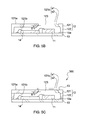
- FIGS. 5A-5C illustrate a method of manufacturing a semiconductor device package 300 in accordance with the embodiment shown in FIG. 3 .
- a carrier 10 having a sensor element 11 disposed thereon or therein is provided.
- a cover 12 is attached to the carrier.
- the cover 12 includes a base substrate 121 defining a penetrating hole 123 , and further includes a periphery barrier 122 .
- the cover 12 is positioned such that the periphery barrier 122 contacts a top surface 10 a of the carrier.
- a filter 13 is attached to a top surface 121 a of the base substrate 121 , for example, by an adhesive, and covers the penetrating hole 123 .
- the semiconductor device package 100 in accordance with the embodiment shown in FIG. 1 can be manufactured in a similar manner as described in FIGS. 5A-5C for the semiconductor device package 300 .
- FIGS. 6A-6C illustrate a method of manufacturing a semiconductor device package 400 in accordance with the embodiment shown in FIG. 4 .
- a carrier 10 having a sensor element 11 disposed thereon or therein is provided in FIG. 6A .
- a cover 12 is attached to the carrier 10 .
- the cover 12 includes a base substrate 121 defining a penetrating hole 123 , a periphery barrier 122 , and a portion 124 protruding from a top surface 121 a of the base substrate 121 .
- the cover 12 is positioned such that the periphery barrier 122 contacts a top surface 10 a of the carrier 10 .
- FIG. 1 a carrier 10 having a sensor element 11 disposed thereon or therein is provided in FIG. 6B .
- the cover 12 includes a base substrate 121 defining a penetrating hole 123 , a periphery barrier 122 , and a portion 124 protruding from a top surface 121
- an adhesive 15 is applied to a space defined by an inner sidewall 124 s of the protruding portion 124 of the cover 12 , and a filter 13 is placed on the top surface 121 a of the base substrate 121 to cover the penetrating hole 123 , the filter 13 being adhered to the top surface 121 a of the base substrate 121 by the adhesive 15 .
- the inner sidewall 124 s of the protruding portion 124 is set back from the inner sidewall 121 s ′, leaving a shelf area on the top surface 121 a of the base substrate 121 on which to apply the adhesive 15 .
- positioning of the adhesive may be better controlled.
- the semiconductor device packages according to the present disclosure can be prepared using existing equipment, and the manufacture is cost-effective.
- the cover 12 can be preformed, such as by molding (e.g., injection molding); and the filter 13 can be applied to the top surface 121 a of the base substrate 121 of the cover 12 , for example, by a pick-and-place machine already present in a semiconductor package plant, and damage to the filter 13 would be avoided during such placement.
- the terms “substantially” and “about” are used to denote small variations.
- the terms can refer to a range of variation of less than or equal to ⁇ 10% of that numerical value, such as less than or equal to ⁇ 5%, less than or equal to ⁇ 4%, less than or equal to ⁇ 3%, less than or equal to ⁇ 2%, less than or equal to ⁇ 1%, less than or equal to ⁇ 0.5%, less than or equal to ⁇ 0.1%, or less than or equal to ⁇ 0.05%.
- substantially and “about” can refer to instances in which the event or circumstance occurs precisely, as well as instances in which the event or circumstance occurs to a close approximation.
- substantially perpendicular can refer to a range of variation of less than or equal to ⁇ 10% of 90°, such as less than or equal to ⁇ 5%, less than or equal to ⁇ 4%, less than or equal to ⁇ 3%, less than or equal to ⁇ 2%, less than or equal to ⁇ 1%, less than or equal to ⁇ 0.5%, less than or equal to ⁇ 0.1%, or less than or equal to ⁇ 0.05%.
Abstract
A semiconductor device package includes a carrier, a sensor element disposed on or within the carrier, a cover and a filter. The cover includes a base substrate and a periphery barrier. The base substrate includes an inner sidewall. The inner sidewall of the base substrate defines a penetrating hole extending from a top surface of the base substrate to a bottom surface of the base substrate; at least a portion of the inner sidewall of the base substrate is tilted. The periphery barrier is coupled to the bottom surface of the base substrate and contacts a top surface of the carrier. The filter is disposed on the top surface of the base substrate and covers the penetrating hole.
Description
1. Technical Field
The present disclosure relates to a semiconductor device package and a method of making the same, and more particularly, to a semiconductor device package having a micro-electro-mechanical systems (MEMS) device and a manufacturing method thereof.
2. Description of the Related Art
Packaging requirements for MEMS devices (such as MEMS dies) can be much more complex than traditional IC packaging requirements. An optical sensor package including a MEMS device is described by way of example. The optical sensor package should include an aperture to allow transmission of light to be detected, while reducing undesired parasitic light. Parasitic light refers to any of the incident light that may cause disturbance to the optical sensor. A MEMS die that allows the passage of light within a specific wavelength range through an aperture may be positioned on or within the optical sensor package adjacent to the aperture, such as on an outer surface of a lid of the MEMS device or on an inner surface of the lid.
When the MEMS die is placed on the inner surface of the lid, such as by pick-and-place, a relatively large distance between the aperture and a sidewall of the lid is needed, to avoid collision during the placement. Alternatively, a special apparatus can be used for placement, but the special apparatus increases manufacturing time and cost.
Additionally, undesired parasitic light may enter the package through an adhesive used to adhere the MEMS die to the lid. To enhance the sensitivity of the sensor, it is desired to reduce parasitic light detected by the sensor.
In an embodiment, a semiconductor device package includes a carrier, a sensor element disposed on or within the carrier, a cover and a filter. The cover includes a base substrate and a periphery barrier. The base substrate includes an inner sidewall. The inner sidewall of the base substrate defines a penetrating hole extending from a top surface of the base substrate to a bottom surface of the base substrate; at least a portion of the inner sidewall of the base substrate is tilted. The periphery barrier is coupled to the bottom surface of the base substrate and is disposed on a top surface of the carrier. The filter is disposed on the top surface of the base substrate and covers the penetrating hole.
In an embodiment, a method of manufacturing a semiconductor device package includes: providing a carrier having a sensor element disposed thereon; and attaching a cover to the carrier, the cover including a base substrate defining a penetrating hole, the cover further including a periphery barrier. The cover is positioned on the carrier such that the periphery barrier of the cover contacts a top surface of the carrier. The method further includes attaching a filter to a top surface of the base substrate of the cover such that the filter covers the penetrating hole.
Common reference numerals are used throughout the drawings and the detailed description to indicate the same or similar components. The present disclosure will be more apparent from the following detailed description taken in conjunction with the accompanying drawings.
The present disclosure describes techniques suitable for the manufacture of smaller sensor device packages without the need of a special apparatus or special apparatuses. For embodiments of an optical sensor, the resulting sensor device packages can reduce parasitic light detected by the sensor, and thus enhance the sensitivity of the sensor.
In one or more embodiments, the carrier 10 is a pre-molded leadframe including a die pad and leads. In one or more embodiments, the leadframe is, or includes, copper or a copper alloy. In other embodiments, the leadframe includes one of, or a combination of, iron, an iron alloy, nickel, a nickel alloy, or another metal or metal alloy. In one or more embodiments, the leadframe is coated with a silver or a copper layer.
In one or more embodiments, the carrier 10 is a substrate. The substrate is, for example, a printed circuit board (PCB), such as a paper-based copper foil laminate, a composite copper foil laminate, or a polymer-impregnated glass-fiber-based copper foil laminate. The substrate can include a core layer which is made of a bismaleimide-triazine (BT) resin or a glass-reinforced epoxy composite (e.g., an FR-4 composite).
In one or more embodiments, the carrier 10 is a semiconductor die. The semiconductor die may be, for example, an application-specific integrated circuit (ASIC) die.
In the embodiment illustrated in FIG. 1 , the sensor element 11 (e.g., an infrared sensor) is disposed on a top surface 10 a of the carrier 10 to sense or detect light passing through the filter 13. In other embodiments, the sensor element 11 is disposed within the carrier 10. The sensor element 11 is electrically connected (e.g., by wire bonding or flip chip bonding) to another device, such as to a processor 14 as shown in FIG. 1 , or such as to an electrode (not shown) of the carrier 10 or other electronic device.
The cover 12 is positioned on the top surface 10 a of the carrier 10. The cover 12 includes a base substrate 121 and a periphery barrier 122. The periphery barrier 122 is coupled to a bottom surface 121 b of the base substrate 121, and contacts the top surface 10 a of the carrier 10. The periphery barrier 122 may be integral with the base substrate 121 of the cover 12, or may be included as a separate component from the cover 12. The cover 12 and the carrier 10 together define a space to accommodate the sensor element 11 and protect the sensor element 11.
The base substrate 121 of the cover 12 has an inner sidewall 121 s. The inner sidewall 121 s of the base substrate 121 defines a penetrating hole 123 extending from a top surface 121 a of the base substrate 121 to the bottom surface 121 b of the base substrate 121.
In one or more embodiments, the cover 12 is, or includes, plastic. For example, the cover 12 may include a liquid crystal polymer, an epoxy resin, a polyphthalamide (PPA) resin, or a combination thereof. In such embodiments, the inner sidewall 121 s, the top surface 121 a and/or the bottom surface 121 b of the base substrate 121 of the cover 12 may be coated with a reflective material for light reflection, and to prevent external light from entering the semiconductor device package 100 through the cover 12. In one or more embodiments, the reflective material is a metal coating; in other embodiments, the reflective material is another material.
In other embodiments, the cover 12 is, or includes, a metal for light reflection, and to prevent external light from entering the semiconductor device package 100 through the cover 12.
The metal used for the cover 12, or for the metal reflective material coated on the cover 12, can be stainless steel, aluminum (Al), gold (Au), silver (Ag), copper (Cu), nickel (Ni), or other metal, or can be a metal composite having a layered structure, such as stainless steel/Ni/Au, Ni/Ag, Ni/Au, stainless steel/Cu/stainless steel, and the like.
The filter 13 is disposed on the top surface 121 a of the base substrate 121 and covers the penetrating hole 123. In one or more embodiments, depending on the intended application for the semiconductor device package 100, the filter 13 can be selected to allow light within a specific wavelength range to pass. In some embodiments, the sensor 11 is an infrared sensor, and the filter 13 allows infrared rays (e.g., near-infrared, middle-infrared or far-infrared rays) to pass, and may block light having other wavelengths. In one or more embodiments, the filter 13 allows infrared rays having a wavelength of about 5 μm or above to pass.
The filter 13 can be made of suitable materials, for example, silicon.
The filter 13 can be applied to the top surface 121 a of the base substrate 121, for example, by a pick-and-place machine, and therefore the filter 13 (and the periphery barrier 122) would not be damaged during placement, as could be the case if the filter 13 were applied on the bottom surface 121 b of the base substrate 121. Accordingly, a distance between the aperture and the inner sidewall can be decreased, without the need to accommodate a placement technique.
An adhesive (not shown) can be used to adhere the filter 13 to the cover 12.
To reduce or minimize undesired parasitic light from entering the package 100, such as from the edge of the filter 13 through the adhesive or by way of undesirable non-normal incident light (as described below), the inner sidewall 121 s of the base substrate 121 is angled, as shown in FIG. 1 . The benefits of this approach are discussed with respect to FIGS. 2A and 2B .
In some embodiments, the sensor element 11 is divided into several sensing areas for receiving light from a corresponding area of an external object, to identify the position or shape of the external object. In such embodiments, it is desirable that most of the received light is normal incident light (i.e., substantially perpendicular to a receiving area of the sensor element 11), because non-normal incident light may cause misjudgment of the sensor element 11. An example of non-normal incident light is when the light comes from the left side of the external object and is received by a sensing area located at the right side of the sensor element 11.
According to the present disclosure, to reduce the undesired parasitic light, as shown in FIG. 1 , the inner sidewall 121 s is tilted at an angle (shown as θ in FIG. 1 ). The angle is less than about 90 degrees.
The titled angle (θ) may be adjusted or optimized in view of one or more of the following factors: a distance between the inner sidewall 121 s and a nearest lateral surface 11 s of the sensor element 11, a distance between the bottom surface 121 b of the base substrate 121 and a top surface 11 a of the sensor element 11, and a size of the penetrating hole 123. In one or more embodiments, the inner sidewall 121 s of the base substrate 121 is tilted at an angle (θ) of between about 10° to less than about 90°, such as about 15° to about 80°, about 20° to about 70°, about 25° to about 65°, about 30° to about 60°, about 35° to about 55°, or about 40° to about 50°, relative to the top surface 121 a of the base substrate 121. In one or more embodiments (e.g., as shown in FIG. 1 ), the inner sidewall 121 s of the base substrate 121 is tilted at an angle of about 45°, such as about 42° to about 48°, relative to the top surface of the base substrate 121.
In one or more embodiments (e.g., as shown in FIG. 1 ), the whole of the inner sidewall 121 s of the base substrate 121 is tilted. In other embodiments, a portion of the inner sidewall 121 s is tilted at an angle, and a portion is not tilted.
The tilted portion s2 is tilted at an angle (θ) of between about 10° to less than about 90°, such as about 15° to about 80°, about 20° to about 70°, about 25° to about 65°, about 30° to about 60°, about 35° to about 55°, or about 40° to about 50°, relative to the top surface 121 a of the base substrate 121. In one or more embodiments (e.g., as shown in FIG. 3 ), the tilted portion s2 of the inner sidewall 121 s′ is tilted at an angle of about 45°, such as about 42° to about 48°, relative to the top surface of the base substrate 121. The tilted portion s2 can change a path of the undesired parasitic light and reduce the amount of the undesired parasitic light received by the sensor element 11.
The combination of a perpendicular portion s1 and a tilted portion s2 (as shown in FIG. 3 ) avoids a sharp edge between the inner sidewall 121 s and the top surface 121 a, as can occur in an embodiment in which the whole of the inner sidewall 121 s of the base substrate 121 is tilted (e.g., as shown in FIG. 1 ). Such a sharp edge may be more susceptible to breakage during handling or manufacture. To further reduce a potential for breakage at edges of the base substrate 121, ones of the edges may be rounded. For example, one or more of the following edges may be rounded: the edge between the inner sidewall 121 s or 121 s′ and the top surface 121 a; an edge between the perpendicular portion s1 and the tilted portion s2; or an edge between the tilted portion s2 and the bottom surface 121 b.
The cover 12 includes a base substrate 121, a periphery barrier 122 and a portion 124 protruding from the top surface 121 a of the base substrate 121. The protruding portion 124 may be integral with the base substrate 121 of the cover 12, or may be included as a separate component from the cover 12. Additionally, as described above with respect to FIG. 1 , the periphery barrier 122 may be integral with the base substrate 121 of the cover 12, or may be included as a separate component from the cover 12. Accordingly, the cover 12 may include one, two, or three components (e.g., one integral component 121/122/124; one integral component 121/122 and one separate component 124; one integral component 121/124 and one separate component 122; or three separate components 121, 122, 124).
As described with respect to FIG. 1 , the base substrate 121 of the cover 12 defines a penetrating hole 123 extending from a top surface 121 a of the base substrate 121 to a bottom surface 121 b of the base substrate 121. Specifically, in the embodiment shown in FIG. 4 , the penetration hole 123 is defined by the inner sidewall 121 s′ of the base substrate 121.
The protruding portion 124 of the cover 12 has an inner sidewall 124 s defining a space to accommodate the filter 13; therefore, it is easier to align the filter.
In one or more embodiments, the inner sidewall 124 s of the protruding portion 124 is substantially perpendicular to the top surface 121 a of the base substrate 121. In other embodiments, the inner sidewall 124 s of the protruding portion 124 is tilted. For example, the inner sidewall 124 s may be tilted at an angle (α) of between about 10° to less than about 90°, such as about 15° to about 80°, about 20° to about 70°, about 25° to about 65°, about 30° to about 60°, about 35° to about 55°, or about 40° to about 50°, relative to the top surface 121 a of the base substrate 121. In one or more embodiments, the inner sidewall 124 s of the protruding portion 124 is tilted at an angle of about 45°, such as about 42° to about 48°, relative to the top surface 121 a of the base substrate 121. The titled inner sidewall 124 s can reduce collision between the filter 13 and the protruding portion 124 during the placement of the filter 13.
A portion of the space defined by the inner sidewall 124 s of the protruding portion 124 is filled with an adhesive 15 that adheres the filter 13 to the top surface 121 a of the base substrate 121 and affixes the filter 13 in the space. The adhesive 15 may be any suitable adhesive. In an embodiment, the adhesive is a conductive adhesive. In an embodiment, the adhesive comprises a binder resin and conductive fillers. For example, the binder resin may be an epoxy resin, a polyimide, a polyacrylate, a polyurethane or a silicone resin, and the conductive fillers may be carbon black, metal (e.g., gold, silver, copper, aluminum, zinc, iron or nickel), metal-coated particles, a conductive compound, or combinations thereof. In one embodiment, the adhesive includes conductive fillers selected from carbon black, metal particles, metal-coated particles and a combination thereof. The adhesive may be selected to minimize undesired parasitic light from entering the package 400.
As described with respect to FIG. 1 , the cover 12 may be plastic or metal, and the cover 12 may be coated with a reflective material. Refer to the description of FIG. 1 for details. As also described with respect to FIGS. 1 and 3 , the base substrate 121 of the cover 12 may respectively have a tilted inner sidewall 121 s, or an inner sidewall 121 s′ including a tilted portion s2. Refer to the respective descriptions of FIGS. 1 and 3 for details. The tilted inner sidewall 121 s or tilted portion s2 of the inner sidewall 121 s′ can change the path of undesired parasitic light and reduce the amount of undesired parasitic light received by the sensor element 11 As noted, the filter 13 is attached to the top surface 121 a of the base substrate 121 by the adhesive 15 filled in a portion of the space defined by the inner sidewall 124 s of the protruding portion 124, and the filter 13 covers the penetrating hole 123. As compared to the embodiments shown in FIG. 1 and FIG. 3 , the protruding portion 124 and the adhesive 15 filled in the space defined by the inner sidewall 124 s of the protruding portion 124 can not only fix the position of the filter 13, but also protect the filter 13 from damage.
As described with respect to FIG. 1 , in one or more embodiments, depending on the intended application for the semiconductor device package 400, the filter 13 can be selected to allow light within a specific wavelength range to pass. In one or more embodiments, the sensor 11 is an infrared sensor, and the filter 13 allows infrared rays (e.g., near-infrared, middle-infrared or far-infrared rays) to pass and may block the light having other wavelength.
The semiconductor device packages (e.g., as shown in FIGS. 1, 3 and 4 ) of the present disclosure can be applied to various MEMS devices, such as MEMS devices used for an infrared camera, a thermopile, a gesture sensor, or a proximity sensor. The techniques described in the present disclosure enhance the sensitivity of the sensor due to the design of the inner sidewall (e.g., 121 s or 121 s′) defining the penetrating hole 123.
The semiconductor device package 100 in accordance with the embodiment shown in FIG. 1 can be manufactured in a similar manner as described in FIGS. 5A-5C for the semiconductor device package 300.
The semiconductor device packages according to the present disclosure can be prepared using existing equipment, and the manufacture is cost-effective. For example, the cover 12 can be preformed, such as by molding (e.g., injection molding); and the filter 13 can be applied to the top surface 121 a of the base substrate 121 of the cover 12, for example, by a pick-and-place machine already present in a semiconductor package plant, and damage to the filter 13 would be avoided during such placement.
The techniques described in the present disclosure result in improved sensor sensitivity.
As used herein, the terms “substantially” and “about” are used to denote small variations. For example, when used in conjunction with a numerical value, the terms can refer to a range of variation of less than or equal to ±10% of that numerical value, such as less than or equal to ±5%, less than or equal to ±4%, less than or equal to ±3%, less than or equal to ±2%, less than or equal to ±1%, less than or equal to ±0.5%, less than or equal to ±0.1%, or less than or equal to ±0.05%. When used in conjunction with an event or circumstance, the terms “substantially” and “about” can refer to instances in which the event or circumstance occurs precisely, as well as instances in which the event or circumstance occurs to a close approximation. For example, “substantially perpendicular” can refer to a range of variation of less than or equal to ±10% of 90°, such as less than or equal to ±5%, less than or equal to ±4%, less than or equal to ±3%, less than or equal to ±2%, less than or equal to ±1%, less than or equal to ±0.5%, less than or equal to ±0.1%, or less than or equal to ±0.05%.
Additionally, amounts, ratios, and other numerical values are sometimes presented herein in a range format. It can be understood that such range formats are used for convenience and brevity, and should be understood flexibly to include not only numerical values explicitly specified as limits of a range, but also all individual numerical values or sub-ranges encompassed within that range as if each numerical value and sub-range is explicitly specified.
While the present disclosure has been described and illustrated with reference to specific embodiments thereof, these descriptions and illustrations do not limit the present disclosure. It can be clearly understood by those skilled in the art that various changes may be made, and equivalent elements may be substituted within the embodiments without departing from the true spirit and scope of the present disclosure as defined by the appended claims. The illustrations may not necessarily be drawn to scale. There may be distinctions between the artistic renditions in the present disclosure and the actual apparatus, due to variables in manufacturing processes and such. There may be other embodiments of the present disclosure which are not specifically illustrated. The specification and drawings are to be regarded as illustrative rather than restrictive. Modifications may be made to adapt a particular situation, material, composition of matter, method, or process to the objective, spirit and scope of the present disclosure. All such modifications are intended to be within the scope of the claims appended hereto. While the methods disclosed herein have been described with reference to particular operations performed in a particular order, it can be understood that these operations may be combined, sub-divided, or re-ordered to form an equivalent method without departing from the teachings of the present disclosure. Therefore, unless specifically indicated herein, the order and grouping of the operations are not limitations of the present disclosure.
Claims (13)
1. A semiconductor device package, comprising:
a carrier having a top surface;
a sensor element disposed on or within the carrier; and
a cover comprising:
a base substrate having a top surface, a bottom surface and an inner sidewall, the inner sidewall defining a penetrating hole extending from the top surface of the base substrate to the bottom surface of the base substrate; and
a periphery barrier coupled to the bottom surface of the base substrate and disposed on the top surface of the carrier; and
a filter disposed on the top surface of the base substrate and covering the penetrating hole;
(i) wherein the inner sidewall of the base substrate is divided into an upper portion and a lower portion, the upper portion is substantially perpendicular to the top surface of the base substrate, and the lower portion is tilted; or
(ii) wherein the entire inner sidewall of the base substrate is tilted; and
wherein the lower portion of the inner sidewall or the entire inner sidewall is tilted at an angle of between about 10° to less than about 90°, relative to the top surface of the base substrate.
2. The semiconductor device package according to claim 1 , wherein the lower portion of the inner sidewall or the entire inner sidewall is tilted at an angle of between about 30° to about 60°, relative to the top surface of the base substrate.
3. The semiconductor device package according to claim 1 , wherein the lower portion of the inner sidewall or the entire inner sidewall is tilted at an angle of between about 40° to about 50°, relative to the top surface of the base substrate.
4. The semiconductor device package according to claim 1 , wherein the cover further comprises a portion protruding from the top surface of the base substrate, and the protruding portion of the cover comprises an inner sidewall defining a space to accommodate the filter.
5. The semiconductor device package according to claim 4 , further comprising an adhesive is filled in the space defined by the inner sidewall of the protruding portion of the cover.
6. The semiconductor device package according to claim 5 , wherein the adhesive comprises conductive fillers selected from carbon black, metal particles, metal-coated particles, or a combination thereof.
7. The semiconductor device package according to claim 4 , wherein the inner sidewall of the protruding portion is tilted.
8. The semiconductor device package according to claim 7 , wherein the inner sidewall of the protruding portion is tilted at an angle of between about 10° to less than about 90°, relative to the top surface of the base substrate.
9. The semiconductor device package according to claim 7 , wherein the inner sidewall of the protruding portion is tilted at an angle of between about 30° to about 60°, relative to the top surface of the base substrate.
10. The semiconductor device package according to claim 7 , wherein the inner sidewall of the protruding portion is tilted at an angle of between about 40° to about 50°, relative to the top surface of the base substrate.
11. The semiconductor device package according to claim 1 , wherein the inner sidewall of the base substrate of the cover and at least one of the bottom surface and the top surface of the base substrate of the cover are light reflection surfaces.
12. The semiconductor device package according to claim 11 , wherein the cover is a plastic cover and the light reflection surfaces are coated with a reflective material.
13. The semiconductor device package according to claim 11 , wherein the cover is a metal cover.
Priority Applications (6)
| Application Number | Priority Date | Filing Date | Title |
|---|---|---|---|
| US14/923,602 US9850124B2 (en) | 2015-10-27 | 2015-10-27 | Semiconductor device package for reducing parasitic light and method of manufacturing the same |
| CN201610969440.7A CN106986298B (en) | 2015-10-27 | 2016-10-27 | Semiconductor device packages and its manufacturing method |
| TW105134860A TWI649859B (en) | 2015-10-27 | 2016-10-27 | Semiconductor device package and method of manufacturing same |
| CN201910446154.6A CN110228786B (en) | 2015-10-27 | 2016-10-27 | Semiconductor device package and method of manufacturing the same |
| US15/815,432 US10526200B2 (en) | 2015-10-27 | 2017-11-16 | Semiconductor device package including cover including tilted inner sidewall |
| US16/735,006 US20200140262A1 (en) | 2015-10-27 | 2020-01-06 | Semiconductor device package and method of manufacturing the same |
Applications Claiming Priority (1)
| Application Number | Priority Date | Filing Date | Title |
|---|---|---|---|
| US14/923,602 US9850124B2 (en) | 2015-10-27 | 2015-10-27 | Semiconductor device package for reducing parasitic light and method of manufacturing the same |
Related Child Applications (1)
| Application Number | Title | Priority Date | Filing Date |
|---|---|---|---|
| US15/815,432 Continuation US10526200B2 (en) | 2015-10-27 | 2017-11-16 | Semiconductor device package including cover including tilted inner sidewall |
Publications (2)
| Publication Number | Publication Date |
|---|---|
| US20170113922A1 US20170113922A1 (en) | 2017-04-27 |
| US9850124B2 true US9850124B2 (en) | 2017-12-26 |
Family
ID=58561865
Family Applications (3)
| Application Number | Title | Priority Date | Filing Date |
|---|---|---|---|
| US14/923,602 Active 2035-10-31 US9850124B2 (en) | 2015-10-27 | 2015-10-27 | Semiconductor device package for reducing parasitic light and method of manufacturing the same |
| US15/815,432 Active US10526200B2 (en) | 2015-10-27 | 2017-11-16 | Semiconductor device package including cover including tilted inner sidewall |
| US16/735,006 Abandoned US20200140262A1 (en) | 2015-10-27 | 2020-01-06 | Semiconductor device package and method of manufacturing the same |
Family Applications After (2)
| Application Number | Title | Priority Date | Filing Date |
|---|---|---|---|
| US15/815,432 Active US10526200B2 (en) | 2015-10-27 | 2017-11-16 | Semiconductor device package including cover including tilted inner sidewall |
| US16/735,006 Abandoned US20200140262A1 (en) | 2015-10-27 | 2020-01-06 | Semiconductor device package and method of manufacturing the same |
Country Status (3)
| Country | Link |
|---|---|
| US (3) | US9850124B2 (en) |
| CN (2) | CN110228786B (en) |
| TW (1) | TWI649859B (en) |
Families Citing this family (10)
| Publication number | Priority date | Publication date | Assignee | Title |
|---|---|---|---|---|
| JP6398810B2 (en) * | 2015-03-12 | 2018-10-03 | オムロン株式会社 | Internal temperature measuring device and temperature difference measuring module |
| JP6398806B2 (en) * | 2015-03-12 | 2018-10-03 | オムロン株式会社 | Sensor package |
| JP6398808B2 (en) * | 2015-03-12 | 2018-10-03 | オムロン株式会社 | Internal temperature measuring device and sensor package |
| TWI699005B (en) * | 2016-11-02 | 2020-07-11 | 原相科技股份有限公司 | Optical component packaging structure |
| FR3075466B1 (en) * | 2017-12-15 | 2020-05-29 | Stmicroelectronics (Grenoble 2) Sas | ELECTRONIC CIRCUIT BOX COVER |
| FR3075465B1 (en) | 2017-12-15 | 2020-03-27 | Stmicroelectronics (Grenoble 2) Sas | ELECTRONIC CIRCUIT BOX COVER |
| DE102018207201A1 (en) | 2018-05-09 | 2019-11-14 | Robert Bosch Gmbh | Manufacturing method for a micromechanical device with inclined optical windows and corresponding micromechanical device |
| US11430906B2 (en) * | 2018-07-26 | 2022-08-30 | Advanced Semiconductor Engineering, Inc. | Optical device including lid having first and second cavity with inclined sidewalls |
| CN111198424A (en) * | 2018-11-16 | 2020-05-26 | 三营超精密光电(晋城)有限公司 | Gasket and lens using same |
| US11515220B2 (en) * | 2019-12-04 | 2022-11-29 | Advanced Semiconductor Engineering, Inc. | Semiconductor package structures and methods of manufacturing the same |
Citations (3)
| Publication number | Priority date | Publication date | Assignee | Title |
|---|---|---|---|---|
| US7285834B2 (en) * | 2001-08-24 | 2007-10-23 | Schott Ag | Process for producing microelectromechanical components and a housed microelectromechanical component |
| US20130181310A1 (en) * | 2012-01-12 | 2013-07-18 | Samsung Electronics Co., Ltd. | Semiconductor apparatus and image sensor package using the same |
| US20140246738A1 (en) | 2013-03-04 | 2014-09-04 | Unisem (M) Berhad | Top Port MEMS Cavity Package and Method of Manufacture Thereof |
Family Cites Families (16)
| Publication number | Priority date | Publication date | Assignee | Title |
|---|---|---|---|---|
| US5458716A (en) * | 1994-05-25 | 1995-10-17 | Texas Instruments Incorporated | Methods for manufacturing a thermally enhanced molded cavity package having a parallel lid |
| US6953891B2 (en) * | 2003-09-16 | 2005-10-11 | Micron Technology, Inc. | Moisture-resistant electronic device package and methods of assembly |
| JP4365743B2 (en) * | 2004-07-27 | 2009-11-18 | 富士通マイクロエレクトロニクス株式会社 | Imaging device |
| CN1278923C (en) * | 2004-09-17 | 2006-10-11 | 中国科学院上海微系统与信息技术研究所 | Once formed atomic force microscope probe and cantilever beam by mask and no-mask technology |
| TW200723551A (en) * | 2005-12-02 | 2007-06-16 | Altus Technology Inc | Image sensor chip package |
| US7608921B2 (en) * | 2006-12-07 | 2009-10-27 | Stats Chippac, Inc. | Multi-layer semiconductor package |
| US20080197435A1 (en) * | 2007-02-21 | 2008-08-21 | Advanced Chip Engineering Technology Inc. | Wafer level image sensor package with die receiving cavity and method of making the same |
| KR100966338B1 (en) * | 2008-07-28 | 2010-06-28 | 삼성전기주식회사 | camera module for Wafer level package |
| US7813043B2 (en) * | 2008-08-15 | 2010-10-12 | Ether Precision, Inc. | Lens assembly and method of manufacture |
| TWM362434U (en) * | 2009-02-27 | 2009-08-01 | Asia Optical Co Inc | Image sensing module |
| KR20110092188A (en) | 2010-02-08 | 2011-08-17 | 이종호 | Fingerprint passbook |
| KR20140028700A (en) * | 2012-08-30 | 2014-03-10 | 삼성전자주식회사 | Semiconductor pakage |
| US20140176570A1 (en) * | 2012-12-21 | 2014-06-26 | Pixtronix, Inc. | Interferometric light absorbing structure for display apparatus |
| CN203259470U (en) * | 2013-05-16 | 2013-10-30 | 江苏物联网研究发展中心 | Monolithic integrated miniature infrared gas sensor |
| JP2015099262A (en) | 2013-11-19 | 2015-05-28 | ソニー株式会社 | Solid state image sensor, camera module and an electronic apparatus |
| US9343443B2 (en) * | 2014-02-05 | 2016-05-17 | Cooledge Lighting, Inc. | Light-emitting dies incorporating wavelength-conversion materials and related methods |
-
2015
- 2015-10-27 US US14/923,602 patent/US9850124B2/en active Active
-
2016
- 2016-10-27 CN CN201910446154.6A patent/CN110228786B/en active Active
- 2016-10-27 TW TW105134860A patent/TWI649859B/en active
- 2016-10-27 CN CN201610969440.7A patent/CN106986298B/en active Active
-
2017
- 2017-11-16 US US15/815,432 patent/US10526200B2/en active Active
-
2020
- 2020-01-06 US US16/735,006 patent/US20200140262A1/en not_active Abandoned
Patent Citations (3)
| Publication number | Priority date | Publication date | Assignee | Title |
|---|---|---|---|---|
| US7285834B2 (en) * | 2001-08-24 | 2007-10-23 | Schott Ag | Process for producing microelectromechanical components and a housed microelectromechanical component |
| US20130181310A1 (en) * | 2012-01-12 | 2013-07-18 | Samsung Electronics Co., Ltd. | Semiconductor apparatus and image sensor package using the same |
| US20140246738A1 (en) | 2013-03-04 | 2014-09-04 | Unisem (M) Berhad | Top Port MEMS Cavity Package and Method of Manufacture Thereof |
Also Published As
| Publication number | Publication date |
|---|---|
| CN110228786B (en) | 2023-09-19 |
| CN106986298B (en) | 2019-06-21 |
| CN106986298A (en) | 2017-07-28 |
| US20170113922A1 (en) | 2017-04-27 |
| US20180072563A1 (en) | 2018-03-15 |
| CN110228786A (en) | 2019-09-13 |
| US20200140262A1 (en) | 2020-05-07 |
| TWI649859B (en) | 2019-02-01 |
| US10526200B2 (en) | 2020-01-07 |
| TW201715710A (en) | 2017-05-01 |
Similar Documents
| Publication | Publication Date | Title |
|---|---|---|
| US10526200B2 (en) | Semiconductor device package including cover including tilted inner sidewall | |
| US11682598B2 (en) | Sensor package and manufacturing method thereof | |
| US9653407B2 (en) | Semiconductor device packages | |
| KR101942141B1 (en) | Package of finger print sensor | |
| US9190367B1 (en) | Semiconductor package structure and semiconductor process | |
| US20180336393A1 (en) | Fingerprint sensing unit | |
| US20140340302A1 (en) | Integrated gesture sensor module | |
| US8251601B2 (en) | Camera module and method for fabricating the same | |
| US9859232B1 (en) | Semiconductor package device and method of manufacturing the same | |
| US9437576B1 (en) | Semiconductor device package and method of manufacturing the same | |
| US20230335533A1 (en) | Semiconductor device package and method for manufacturing the same | |
| US20190081028A1 (en) | Optical module, module, and methods for manufacturing optical module and module | |
| US20180350753A1 (en) | Semiconductor package device and method of manufacturing the same | |
| US10689249B2 (en) | Semiconductor device package including a wall and a grounding ring exposed from the wall | |
| US20220005779A1 (en) | Semiconductor device and manufacturing method thereof | |
| US10115673B1 (en) | Embedded substrate package structure | |
| US10373883B2 (en) | Semiconductor package device and method of manufacturing the same | |
| US20080122059A1 (en) | Stacked chip package structure and fabricating method thereof | |
| US20200335452A1 (en) | Semiconductor device package and method of manufacturing the same | |
| US11276797B2 (en) | Optical device and method of manufacturing the same | |
| US20240038677A1 (en) | Semiconductor device package and method of manufacturing the same | |
| KR20150090705A (en) | Sensor Package and the Method of Manufacturing the same |
Legal Events
| Date | Code | Title | Description |
|---|---|---|---|
| AS | Assignment |
Owner name: ADVANCED SEMICONDUCTOR ENGINEERING, INC., TAIWAN Free format text: ASSIGNMENT OF ASSIGNORS INTEREST;ASSIGNORS:HUANG, CHING-HAN;CHAN, HSUN-WEI;TSAI, YU-HSUAN;REEL/FRAME:037247/0301 Effective date: 20151021 |
|
| STCF | Information on status: patent grant |
Free format text: PATENTED CASE |
|
| MAFP | Maintenance fee payment |
Free format text: PAYMENT OF MAINTENANCE FEE, 4TH YEAR, LARGE ENTITY (ORIGINAL EVENT CODE: M1551); ENTITY STATUS OF PATENT OWNER: LARGE ENTITY Year of fee payment: 4 |