US9842927B1 - Integrated circuit structure without gate contact and method of forming same - Google Patents
Integrated circuit structure without gate contact and method of forming same Download PDFInfo
- Publication number
- US9842927B1 US9842927B1 US15/248,367 US201615248367A US9842927B1 US 9842927 B1 US9842927 B1 US 9842927B1 US 201615248367 A US201615248367 A US 201615248367A US 9842927 B1 US9842927 B1 US 9842927B1
- Authority
- US
- United States
- Prior art keywords
- gate
- forming
- source
- dielectric layer
- layer
- Prior art date
- Legal status (The legal status is an assumption and is not a legal conclusion. Google has not performed a legal analysis and makes no representation as to the accuracy of the status listed.)
- Active
Links
- 238000000034 method Methods 0.000 title claims description 54
- 125000006850 spacer group Chemical group 0.000 claims abstract description 79
- 239000004065 semiconductor Substances 0.000 claims description 20
- 229910021332 silicide Inorganic materials 0.000 claims description 20
- FVBUAEGBCNSCDD-UHFFFAOYSA-N silicide(4-) Chemical group [Si-4] FVBUAEGBCNSCDD-UHFFFAOYSA-N 0.000 claims description 20
- 238000002955 isolation Methods 0.000 claims description 3
- 239000010410 layer Substances 0.000 description 218
- 239000000463 material Substances 0.000 description 113
- 239000004020 conductor Substances 0.000 description 44
- 239000003870 refractory metal Substances 0.000 description 28
- 238000000151 deposition Methods 0.000 description 27
- 238000005530 etching Methods 0.000 description 25
- 229910052751 metal Inorganic materials 0.000 description 25
- 239000002184 metal Substances 0.000 description 25
- 230000008021 deposition Effects 0.000 description 17
- IJGRMHOSHXDMSA-UHFFFAOYSA-N Atomic nitrogen Chemical compound N#N IJGRMHOSHXDMSA-UHFFFAOYSA-N 0.000 description 15
- 230000015572 biosynthetic process Effects 0.000 description 15
- VYPSYNLAJGMNEJ-UHFFFAOYSA-N Silicium dioxide Chemical compound O=[Si]=O VYPSYNLAJGMNEJ-UHFFFAOYSA-N 0.000 description 13
- 239000002019 doping agent Substances 0.000 description 10
- 230000008569 process Effects 0.000 description 10
- 239000000758 substrate Substances 0.000 description 9
- 229910052581 Si3N4 Inorganic materials 0.000 description 8
- XUIMIQQOPSSXEZ-UHFFFAOYSA-N Silicon Chemical compound [Si] XUIMIQQOPSSXEZ-UHFFFAOYSA-N 0.000 description 8
- 229910052757 nitrogen Inorganic materials 0.000 description 8
- 229910052710 silicon Inorganic materials 0.000 description 8
- 239000010703 silicon Substances 0.000 description 8
- -1 e.g. Substances 0.000 description 6
- 125000004429 atom Chemical group 0.000 description 5
- 230000004888 barrier function Effects 0.000 description 5
- 238000005229 chemical vapour deposition Methods 0.000 description 5
- 239000000377 silicon dioxide Substances 0.000 description 5
- 235000012239 silicon dioxide Nutrition 0.000 description 5
- HQVNEWCFYHHQES-UHFFFAOYSA-N silicon nitride Chemical compound N12[Si]34N5[Si]62N3[Si]51N64 HQVNEWCFYHHQES-UHFFFAOYSA-N 0.000 description 5
- OKTJSMMVPCPJKN-UHFFFAOYSA-N Carbon Chemical compound [C] OKTJSMMVPCPJKN-UHFFFAOYSA-N 0.000 description 4
- NRTOMJZYCJJWKI-UHFFFAOYSA-N Titanium nitride Chemical compound [Ti]#N NRTOMJZYCJJWKI-UHFFFAOYSA-N 0.000 description 4
- 229910052799 carbon Inorganic materials 0.000 description 4
- 239000012212 insulator Substances 0.000 description 4
- 239000000126 substance Substances 0.000 description 4
- ZOXJGFHDIHLPTG-UHFFFAOYSA-N Boron Chemical compound [B] ZOXJGFHDIHLPTG-UHFFFAOYSA-N 0.000 description 3
- RTAQQCXQSZGOHL-UHFFFAOYSA-N Titanium Chemical compound [Ti] RTAQQCXQSZGOHL-UHFFFAOYSA-N 0.000 description 3
- 238000000231 atomic layer deposition Methods 0.000 description 3
- 229910052796 boron Inorganic materials 0.000 description 3
- 238000006243 chemical reaction Methods 0.000 description 3
- 230000001419 dependent effect Effects 0.000 description 3
- 229910052735 hafnium Inorganic materials 0.000 description 3
- 239000007769 metal material Substances 0.000 description 3
- 150000002739 metals Chemical class 0.000 description 3
- 230000003647 oxidation Effects 0.000 description 3
- 238000007254 oxidation reaction Methods 0.000 description 3
- 238000004544 sputter deposition Methods 0.000 description 3
- 238000000992 sputter etching Methods 0.000 description 3
- 229910052715 tantalum Inorganic materials 0.000 description 3
- GUVRBAGPIYLISA-UHFFFAOYSA-N tantalum atom Chemical compound [Ta] GUVRBAGPIYLISA-UHFFFAOYSA-N 0.000 description 3
- 229910052719 titanium Inorganic materials 0.000 description 3
- 239000010936 titanium Substances 0.000 description 3
- 229910052721 tungsten Inorganic materials 0.000 description 3
- 239000010937 tungsten Substances 0.000 description 3
- JBRZTFJDHDCESZ-UHFFFAOYSA-N AsGa Chemical compound [As]#[Ga] JBRZTFJDHDCESZ-UHFFFAOYSA-N 0.000 description 2
- RTZKZFJDLAIYFH-UHFFFAOYSA-N Diethyl ether Chemical compound CCOCC RTZKZFJDLAIYFH-UHFFFAOYSA-N 0.000 description 2
- GYHNNYVSQQEPJS-UHFFFAOYSA-N Gallium Chemical compound [Ga] GYHNNYVSQQEPJS-UHFFFAOYSA-N 0.000 description 2
- PXHVJJICTQNCMI-UHFFFAOYSA-N Nickel Chemical compound [Ni] PXHVJJICTQNCMI-UHFFFAOYSA-N 0.000 description 2
- BPQQTUXANYXVAA-UHFFFAOYSA-N Orthosilicate Chemical compound [O-][Si]([O-])([O-])[O-] BPQQTUXANYXVAA-UHFFFAOYSA-N 0.000 description 2
- 229910000577 Silicon-germanium Inorganic materials 0.000 description 2
- LEVVHYCKPQWKOP-UHFFFAOYSA-N [Si].[Ge] Chemical compound [Si].[Ge] LEVVHYCKPQWKOP-UHFFFAOYSA-N 0.000 description 2
- 229910052787 antimony Inorganic materials 0.000 description 2
- WATWJIUSRGPENY-UHFFFAOYSA-N antimony atom Chemical compound [Sb] WATWJIUSRGPENY-UHFFFAOYSA-N 0.000 description 2
- 229910052785 arsenic Inorganic materials 0.000 description 2
- RQNWIZPPADIBDY-UHFFFAOYSA-N arsenic atom Chemical compound [As] RQNWIZPPADIBDY-UHFFFAOYSA-N 0.000 description 2
- 239000005380 borophosphosilicate glass Substances 0.000 description 2
- 239000007795 chemical reaction product Substances 0.000 description 2
- 229910052802 copper Inorganic materials 0.000 description 2
- 239000010949 copper Substances 0.000 description 2
- 239000013078 crystal Substances 0.000 description 2
- 238000005137 deposition process Methods 0.000 description 2
- 239000003989 dielectric material Substances 0.000 description 2
- 238000005516 engineering process Methods 0.000 description 2
- 229910052733 gallium Inorganic materials 0.000 description 2
- 239000011521 glass Substances 0.000 description 2
- VBJZVLUMGGDVMO-UHFFFAOYSA-N hafnium atom Chemical compound [Hf] VBJZVLUMGGDVMO-UHFFFAOYSA-N 0.000 description 2
- BHEPBYXIRTUNPN-UHFFFAOYSA-N hydridophosphorus(.) (triplet) Chemical compound [PH] BHEPBYXIRTUNPN-UHFFFAOYSA-N 0.000 description 2
- 229910052738 indium Inorganic materials 0.000 description 2
- APFVFJFRJDLVQX-UHFFFAOYSA-N indium atom Chemical compound [In] APFVFJFRJDLVQX-UHFFFAOYSA-N 0.000 description 2
- 150000002500 ions Chemical class 0.000 description 2
- MRELNEQAGSRDBK-UHFFFAOYSA-N lanthanum(3+);oxygen(2-) Chemical compound [O-2].[O-2].[O-2].[La+3].[La+3] MRELNEQAGSRDBK-UHFFFAOYSA-N 0.000 description 2
- 238000004518 low pressure chemical vapour deposition Methods 0.000 description 2
- 238000004519 manufacturing process Methods 0.000 description 2
- 150000004767 nitrides Chemical class 0.000 description 2
- 238000005240 physical vapour deposition Methods 0.000 description 2
- 238000000623 plasma-assisted chemical vapour deposition Methods 0.000 description 2
- 229920000412 polyarylene Polymers 0.000 description 2
- 239000000047 product Substances 0.000 description 2
- 238000001289 rapid thermal chemical vapour deposition Methods 0.000 description 2
- 239000011669 selenium Substances 0.000 description 2
- 229910052814 silicon oxide Inorganic materials 0.000 description 2
- 239000002356 single layer Substances 0.000 description 2
- MZLGASXMSKOWSE-UHFFFAOYSA-N tantalum nitride Chemical compound [Ta]#N MZLGASXMSKOWSE-UHFFFAOYSA-N 0.000 description 2
- WFKWXMTUELFFGS-UHFFFAOYSA-N tungsten Chemical compound [W] WFKWXMTUELFFGS-UHFFFAOYSA-N 0.000 description 2
- 238000000038 ultrahigh vacuum chemical vapour deposition Methods 0.000 description 2
- 238000001039 wet etching Methods 0.000 description 2
- RYGMFSIKBFXOCR-UHFFFAOYSA-N Copper Chemical compound [Cu] RYGMFSIKBFXOCR-UHFFFAOYSA-N 0.000 description 1
- 229910052692 Dysprosium Inorganic materials 0.000 description 1
- 239000004593 Epoxy Substances 0.000 description 1
- 229910052688 Gadolinium Inorganic materials 0.000 description 1
- ZOKXTWBITQBERF-UHFFFAOYSA-N Molybdenum Chemical compound [Mo] ZOKXTWBITQBERF-UHFFFAOYSA-N 0.000 description 1
- 239000004642 Polyimide Substances 0.000 description 1
- BUGBHKTXTAQXES-UHFFFAOYSA-N Selenium Chemical compound [Se] BUGBHKTXTAQXES-UHFFFAOYSA-N 0.000 description 1
- NINIDFKCEFEMDL-UHFFFAOYSA-N Sulfur Chemical compound [S] NINIDFKCEFEMDL-UHFFFAOYSA-N 0.000 description 1
- 239000005864 Sulphur Substances 0.000 description 1
- ATJFFYVFTNAWJD-UHFFFAOYSA-N Tin Chemical compound [Sn] ATJFFYVFTNAWJD-UHFFFAOYSA-N 0.000 description 1
- GWEVSGVZZGPLCZ-UHFFFAOYSA-N Titan oxide Chemical compound O=[Ti]=O GWEVSGVZZGPLCZ-UHFFFAOYSA-N 0.000 description 1
- 229910052769 Ytterbium Inorganic materials 0.000 description 1
- HMDDXIMCDZRSNE-UHFFFAOYSA-N [C].[Si] Chemical compound [C].[Si] HMDDXIMCDZRSNE-UHFFFAOYSA-N 0.000 description 1
- CEPICIBPGDWCRU-UHFFFAOYSA-N [Si].[Hf] Chemical compound [Si].[Hf] CEPICIBPGDWCRU-UHFFFAOYSA-N 0.000 description 1
- UGACIEPFGXRWCH-UHFFFAOYSA-N [Si].[Ti] Chemical compound [Si].[Ti] UGACIEPFGXRWCH-UHFFFAOYSA-N 0.000 description 1
- 239000002253 acid Substances 0.000 description 1
- VYBYZVVRYQDCGQ-UHFFFAOYSA-N alumane;hafnium Chemical compound [AlH3].[Hf] VYBYZVVRYQDCGQ-UHFFFAOYSA-N 0.000 description 1
- 229910052782 aluminium Inorganic materials 0.000 description 1
- XAGFODPZIPBFFR-UHFFFAOYSA-N aluminium Chemical compound [Al] XAGFODPZIPBFFR-UHFFFAOYSA-N 0.000 description 1
- 229910003481 amorphous carbon Inorganic materials 0.000 description 1
- 229910021417 amorphous silicon Inorganic materials 0.000 description 1
- 238000000137 annealing Methods 0.000 description 1
- QVGXLLKOCUKJST-UHFFFAOYSA-N atomic oxygen Chemical compound [O] QVGXLLKOCUKJST-UHFFFAOYSA-N 0.000 description 1
- IVHJCRXBQPGLOV-UHFFFAOYSA-N azanylidynetungsten Chemical compound [W]#N IVHJCRXBQPGLOV-UHFFFAOYSA-N 0.000 description 1
- 239000000919 ceramic Substances 0.000 description 1
- 238000003486 chemical etching Methods 0.000 description 1
- 229910017052 cobalt Inorganic materials 0.000 description 1
- 239000010941 cobalt Substances 0.000 description 1
- GUTLYIVDDKVIGB-UHFFFAOYSA-N cobalt atom Chemical compound [Co] GUTLYIVDDKVIGB-UHFFFAOYSA-N 0.000 description 1
- 238000010276 construction Methods 0.000 description 1
- 238000001312 dry etching Methods 0.000 description 1
- KBQHZAAAGSGFKK-UHFFFAOYSA-N dysprosium atom Chemical compound [Dy] KBQHZAAAGSGFKK-UHFFFAOYSA-N 0.000 description 1
- 238000000313 electron-beam-induced deposition Methods 0.000 description 1
- 125000003700 epoxy group Chemical group 0.000 description 1
- 150000002170 ethers Chemical class 0.000 description 1
- 238000001704 evaporation Methods 0.000 description 1
- 230000008020 evaporation Effects 0.000 description 1
- 230000005669 field effect Effects 0.000 description 1
- 239000003574 free electron Substances 0.000 description 1
- UIWYJDYFSGRHKR-UHFFFAOYSA-N gadolinium atom Chemical compound [Gd] UIWYJDYFSGRHKR-UHFFFAOYSA-N 0.000 description 1
- 239000007789 gas Substances 0.000 description 1
- 229910000449 hafnium oxide Inorganic materials 0.000 description 1
- WIHZLLGSGQNAGK-UHFFFAOYSA-N hafnium(4+);oxygen(2-) Chemical compound [O-2].[O-2].[Hf+4] WIHZLLGSGQNAGK-UHFFFAOYSA-N 0.000 description 1
- 229910052739 hydrogen Inorganic materials 0.000 description 1
- 239000001257 hydrogen Substances 0.000 description 1
- 125000004435 hydrogen atom Chemical class [H]* 0.000 description 1
- 239000007943 implant Substances 0.000 description 1
- 230000006872 improvement Effects 0.000 description 1
- 239000011810 insulating material Substances 0.000 description 1
- 239000013067 intermediate product Substances 0.000 description 1
- 238000007737 ion beam deposition Methods 0.000 description 1
- 229910052746 lanthanum Inorganic materials 0.000 description 1
- FZLIPJUXYLNCLC-UHFFFAOYSA-N lanthanum atom Chemical compound [La] FZLIPJUXYLNCLC-UHFFFAOYSA-N 0.000 description 1
- 239000007788 liquid Substances 0.000 description 1
- 230000000873 masking effect Effects 0.000 description 1
- 238000002844 melting Methods 0.000 description 1
- 239000000203 mixture Substances 0.000 description 1
- 238000012986 modification Methods 0.000 description 1
- 230000004048 modification Effects 0.000 description 1
- 238000001451 molecular beam epitaxy Methods 0.000 description 1
- 229910052750 molybdenum Inorganic materials 0.000 description 1
- 239000011733 molybdenum Substances 0.000 description 1
- 230000007935 neutral effect Effects 0.000 description 1
- 229910052759 nickel Inorganic materials 0.000 description 1
- QJGQUHMNIGDVPM-UHFFFAOYSA-N nitrogen group Chemical group [N] QJGQUHMNIGDVPM-UHFFFAOYSA-N 0.000 description 1
- 229910052756 noble gas Inorganic materials 0.000 description 1
- 150000002835 noble gases Chemical class 0.000 description 1
- TWNQGVIAIRXVLR-UHFFFAOYSA-N oxo(oxoalumanyloxy)alumane Chemical compound O=[Al]O[Al]=O TWNQGVIAIRXVLR-UHFFFAOYSA-N 0.000 description 1
- SIWVEOZUMHYXCS-UHFFFAOYSA-N oxo(oxoyttriooxy)yttrium Chemical compound O=[Y]O[Y]=O SIWVEOZUMHYXCS-UHFFFAOYSA-N 0.000 description 1
- 229910052760 oxygen Inorganic materials 0.000 description 1
- 239000001301 oxygen Substances 0.000 description 1
- RVTZCBVAJQQJTK-UHFFFAOYSA-N oxygen(2-);zirconium(4+) Chemical compound [O-2].[O-2].[Zr+4] RVTZCBVAJQQJTK-UHFFFAOYSA-N 0.000 description 1
- 239000002245 particle Substances 0.000 description 1
- 229920002120 photoresistant polymer Polymers 0.000 description 1
- 238000005268 plasma chemical vapour deposition Methods 0.000 description 1
- 238000001020 plasma etching Methods 0.000 description 1
- 239000004033 plastic Substances 0.000 description 1
- 238000007747 plating Methods 0.000 description 1
- 238000005498 polishing Methods 0.000 description 1
- 229910021420 polycrystalline silicon Inorganic materials 0.000 description 1
- 229920000647 polyepoxide Polymers 0.000 description 1
- 229920001721 polyimide Polymers 0.000 description 1
- 239000002861 polymer material Substances 0.000 description 1
- 229920005591 polysilicon Polymers 0.000 description 1
- 239000000376 reactant Substances 0.000 description 1
- 230000009467 reduction Effects 0.000 description 1
- 229920005989 resin Polymers 0.000 description 1
- 239000011347 resin Substances 0.000 description 1
- 229910052711 selenium Inorganic materials 0.000 description 1
- 150000003376 silicon Chemical class 0.000 description 1
- HWEYZGSCHQNNEH-UHFFFAOYSA-N silicon tantalum Chemical compound [Si].[Ta] HWEYZGSCHQNNEH-UHFFFAOYSA-N 0.000 description 1
- 239000002904 solvent Substances 0.000 description 1
- 230000003068 static effect Effects 0.000 description 1
- 229920001187 thermosetting polymer Polymers 0.000 description 1
- OGIDPMRJRNCKJF-UHFFFAOYSA-N titanium oxide Inorganic materials [Ti]=O OGIDPMRJRNCKJF-UHFFFAOYSA-N 0.000 description 1
- NAWDYIZEMPQZHO-UHFFFAOYSA-N ytterbium Chemical compound [Yb] NAWDYIZEMPQZHO-UHFFFAOYSA-N 0.000 description 1
- 229910001928 zirconium oxide Inorganic materials 0.000 description 1
- GFQYVLUOOAAOGM-UHFFFAOYSA-N zirconium(iv) silicate Chemical compound [Zr+4].[O-][Si]([O-])([O-])[O-] GFQYVLUOOAAOGM-UHFFFAOYSA-N 0.000 description 1
Images


Classifications
-
- H—ELECTRICITY
- H01—ELECTRIC ELEMENTS
- H01L—SEMICONDUCTOR DEVICES NOT COVERED BY CLASS H10
- H01L29/00—Semiconductor devices adapted for rectifying, amplifying, oscillating or switching, or capacitors or resistors with at least one potential-jump barrier or surface barrier, e.g. PN junction depletion layer or carrier concentration layer; Details of semiconductor bodies or of electrodes thereof ; Multistep manufacturing processes therefor
- H01L29/66—Types of semiconductor device ; Multistep manufacturing processes therefor
- H01L29/68—Types of semiconductor device ; Multistep manufacturing processes therefor controllable by only the electric current supplied, or only the electric potential applied, to an electrode which does not carry the current to be rectified, amplified or switched
- H01L29/76—Unipolar devices, e.g. field effect transistors
- H01L29/772—Field effect transistors
- H01L29/78—Field effect transistors with field effect produced by an insulated gate
- H01L29/783—Field effect transistors with field effect produced by an insulated gate comprising a gate to body connection, i.e. bulk dynamic threshold voltage MOSFET
-
- H—ELECTRICITY
- H01—ELECTRIC ELEMENTS
- H01L—SEMICONDUCTOR DEVICES NOT COVERED BY CLASS H10
- H01L29/00—Semiconductor devices adapted for rectifying, amplifying, oscillating or switching, or capacitors or resistors with at least one potential-jump barrier or surface barrier, e.g. PN junction depletion layer or carrier concentration layer; Details of semiconductor bodies or of electrodes thereof ; Multistep manufacturing processes therefor
- H01L29/40—Electrodes ; Multistep manufacturing processes therefor
- H01L29/41—Electrodes ; Multistep manufacturing processes therefor characterised by their shape, relative sizes or dispositions
- H01L29/417—Electrodes ; Multistep manufacturing processes therefor characterised by their shape, relative sizes or dispositions carrying the current to be rectified, amplified or switched
- H01L29/41725—Source or drain electrodes for field effect devices
- H01L29/41775—Source or drain electrodes for field effect devices characterised by the proximity or the relative position of the source or drain electrode and the gate electrode, e.g. the source or drain electrode separated from the gate electrode by side-walls or spreading around or above the gate electrode
-
- H—ELECTRICITY
- H01—ELECTRIC ELEMENTS
- H01L—SEMICONDUCTOR DEVICES NOT COVERED BY CLASS H10
- H01L29/00—Semiconductor devices adapted for rectifying, amplifying, oscillating or switching, or capacitors or resistors with at least one potential-jump barrier or surface barrier, e.g. PN junction depletion layer or carrier concentration layer; Details of semiconductor bodies or of electrodes thereof ; Multistep manufacturing processes therefor
- H01L29/40—Electrodes ; Multistep manufacturing processes therefor
- H01L29/41—Electrodes ; Multistep manufacturing processes therefor characterised by their shape, relative sizes or dispositions
- H01L29/417—Electrodes ; Multistep manufacturing processes therefor characterised by their shape, relative sizes or dispositions carrying the current to be rectified, amplified or switched
- H01L29/41725—Source or drain electrodes for field effect devices
- H01L29/41791—Source or drain electrodes for field effect devices for transistors with a horizontal current flow in a vertical sidewall, e.g. FinFET, MuGFET
-
- H—ELECTRICITY
- H01—ELECTRIC ELEMENTS
- H01L—SEMICONDUCTOR DEVICES NOT COVERED BY CLASS H10
- H01L29/00—Semiconductor devices adapted for rectifying, amplifying, oscillating or switching, or capacitors or resistors with at least one potential-jump barrier or surface barrier, e.g. PN junction depletion layer or carrier concentration layer; Details of semiconductor bodies or of electrodes thereof ; Multistep manufacturing processes therefor
- H01L29/40—Electrodes ; Multistep manufacturing processes therefor
- H01L29/43—Electrodes ; Multistep manufacturing processes therefor characterised by the materials of which they are formed
- H01L29/49—Metal-insulator-semiconductor electrodes, e.g. gates of MOSFET
- H01L29/4966—Metal-insulator-semiconductor electrodes, e.g. gates of MOSFET the conductor material next to the insulator being a composite material, e.g. organic material, TiN, MoSi2
- H01L29/4975—Metal-insulator-semiconductor electrodes, e.g. gates of MOSFET the conductor material next to the insulator being a composite material, e.g. organic material, TiN, MoSi2 being a silicide layer, e.g. TiSi2
-
- H—ELECTRICITY
- H01—ELECTRIC ELEMENTS
- H01L—SEMICONDUCTOR DEVICES NOT COVERED BY CLASS H10
- H01L29/00—Semiconductor devices adapted for rectifying, amplifying, oscillating or switching, or capacitors or resistors with at least one potential-jump barrier or surface barrier, e.g. PN junction depletion layer or carrier concentration layer; Details of semiconductor bodies or of electrodes thereof ; Multistep manufacturing processes therefor
- H01L29/66—Types of semiconductor device ; Multistep manufacturing processes therefor
- H01L29/66007—Multistep manufacturing processes
- H01L29/66075—Multistep manufacturing processes of devices having semiconductor bodies comprising group 14 or group 13/15 materials
- H01L29/66227—Multistep manufacturing processes of devices having semiconductor bodies comprising group 14 or group 13/15 materials the devices being controllable only by the electric current supplied or the electric potential applied, to an electrode which does not carry the current to be rectified, amplified or switched, e.g. three-terminal devices
- H01L29/66409—Unipolar field-effect transistors
- H01L29/66477—Unipolar field-effect transistors with an insulated gate, i.e. MISFET
- H01L29/66545—Unipolar field-effect transistors with an insulated gate, i.e. MISFET using a dummy, i.e. replacement gate in a process wherein at least a part of the final gate is self aligned to the dummy gate
-
- H—ELECTRICITY
- H01—ELECTRIC ELEMENTS
- H01L—SEMICONDUCTOR DEVICES NOT COVERED BY CLASS H10
- H01L29/00—Semiconductor devices adapted for rectifying, amplifying, oscillating or switching, or capacitors or resistors with at least one potential-jump barrier or surface barrier, e.g. PN junction depletion layer or carrier concentration layer; Details of semiconductor bodies or of electrodes thereof ; Multistep manufacturing processes therefor
- H01L29/66—Types of semiconductor device ; Multistep manufacturing processes therefor
- H01L29/66007—Multistep manufacturing processes
- H01L29/66075—Multistep manufacturing processes of devices having semiconductor bodies comprising group 14 or group 13/15 materials
- H01L29/66227—Multistep manufacturing processes of devices having semiconductor bodies comprising group 14 or group 13/15 materials the devices being controllable only by the electric current supplied or the electric potential applied, to an electrode which does not carry the current to be rectified, amplified or switched, e.g. three-terminal devices
- H01L29/66409—Unipolar field-effect transistors
- H01L29/66477—Unipolar field-effect transistors with an insulated gate, i.e. MISFET
- H01L29/66787—Unipolar field-effect transistors with an insulated gate, i.e. MISFET with a gate at the side of the channel
- H01L29/66795—Unipolar field-effect transistors with an insulated gate, i.e. MISFET with a gate at the side of the channel with a horizontal current flow in a vertical sidewall of a semiconductor body, e.g. FinFET, MuGFET
-
- H—ELECTRICITY
- H10—SEMICONDUCTOR DEVICES; ELECTRIC SOLID-STATE DEVICES NOT OTHERWISE PROVIDED FOR
- H10B—ELECTRONIC MEMORY DEVICES
- H10B10/00—Static random access memory [SRAM] devices
- H10B10/12—Static random access memory [SRAM] devices comprising a MOSFET load element
Definitions
- the present disclosure relates to integrated circuit structures, and more particularly, to an integrated circuit structure without a gate contact and method of forming the same.
- a FET generally includes source, drain, and gate terminals. The gate terminal is placed between the source and drain terminals and controls the current therebetween.
- Transistors may be formed over a substrate and may be electrically isolated with an insulating dielectric layer, e.g., inter-level dielectric layer. Contacts may be formed to each of the source, drain, and gate terminals through the dielectric layer in order to provide electrical connection between the transistors and other circuit elements that may be formed subsequent to the transistor in other metal levels.
- a first aspect of the disclosure provides for a method of forming an integrated circuit structure.
- the method may include: removing a dummy gate stack from between a pair of gate spacers within a dielectric layer thereby forming a first opening within the dielectric layer, the first opening exposing a portion of a fin and a portion of a shallow trench isolation (STI) region that is adjacent to the fin; forming a gate structure within the first opening; forming a second opening within the dielectric layer to expose a source/drain region within the fin, the second opening being adjacent to the gate structure; and forming a source/drain contact within the second opening to the source/drain region.
- STI shallow trench isolation
- a second aspect of the disclosure provides for an integrated circuit structure.
- the integrated circuit structure may include: a gate structure between a pair of gate spacers within a dielectric layer and substantially surrounding a fin, wherein the gate structure is disposed adjacent to a channel region within the fin; and a source/drain contact extending within the dielectric layer to a source/drain region within a fin, the source/drain contact being separated from the gate structure by at least one gate spacer in the pair of gate spacers, wherein the channel region and the source/drain region provide electrical connection between the gate structure and the source/drain contact.
- a third aspect of the disclosure provides for an integrated circuit structure.
- the integrated circuit structure may include: a source/drain contact to a source/drain region, the source/drain contact being adjacent to a gate structure and being directly connected to a gate conductor of the gate structure through a sidewall of the gate structure.
- FIGS. 1-6 show a preliminary integrated circuit (IC) structure undergoing aspects of a method according to one embodiment of the disclosure.
- FIGS. 7-8 show the preliminary IC structure of FIG. 6 undergoing aspects of a method in which a silicide region is formed.
- FIGS. 9-10 show the preliminary IC structure of FIG. 6 undergoing aspects of a method in which an opening is expanded such that the opening is self-aligned with a pair of gate spacers.
- FIG. 11 shows the IC structure of FIG. 8 wherein a gate cap layer is formed.
- FIG. 12 shows the IC structure of FIG. 10 wherein a gate cap layer is formed.
- FIG. 13 shows the IC structure of FIG. 11 wherein an opening is formed within a dielectric layer to expose the source/drain region.
- FIG. 14 shows the IC structure of FIG. 12 wherein an opening is formed within a dielectric layer to expose the source/drain region.
- FIG. 15 shows the IC structure of FIG. 13 wherein a source/drain contact is formed within the dielectric layer to the source/drain region.
- FIG. 16 shows the IC structure of FIG. 14 wherein a source/drain contact is formed within the dielectric layer to the source/drain region.
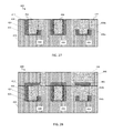
- FIGS. 17-20 show the preliminary IC structure of FIG. 5 undergoing aspects of a method according to another embodiment of the disclosure.
- FIGS. 21-24 show the preliminary IC structure of FIG. 4 undergoing aspects of a method according to another embodiment of the disclosure.
- FIGS. 25-28 show an IC structure undergoing aspects of a method according to another embodiment of the disclosure where FIG. 28 shows a resulting IC structure.
- the present disclosure relates to an integrated circuit (IC) structure, and more particularly, to an integrated circuit structure without a gate contact and method of forming the same.
- IC integrated circuit
- FIG. 1 shows a preliminary IC structure 100 .
- IC structure 100 may be a Static Random Access Memory (SRAM) fin-shaped field effect transistor (FinFET).
- SRAM Static Random Access Memory
- FinFET fin-shaped field effect transistor
- IC structure 100 may include fins 102 substantially isolated from one another by a shallow trench isolation (STI) region 104 . Fins 102 may be patterned and etched from a substrate (not shown) as known in the art. Further, a trench (not shown) may be patterned and etched into the substrate between adjacent fins.
- An insulator e.g., silicon dioxide, may be formed, e.g., deposited, to form STI region 104 .
- STI region 104 separates or isolates adjacent semiconductor devices that are on the same plane from one another. STI region 104 prevents electrical current leakage from the adjacent semiconductor devices, e.g., fins 102 . After deposition of the insulator, the insulator may be annealed to form STI region 104 as is known in the art.
- substantially refers to largely, for the most part, entirely specified or any slight deviation which provides the same technical benefits of the invention.
- approximately is intended to include values, for example, within 10% of the stated values.
- the term “depositing” may include any now known or later developed technique appropriate for deposition, including but not limited to, for example: chemical vapor deposition (CVD), low-pressure CVD (LPCVD), plasma-enhanced CVD (PECVD), semi-atmosphere CVD (SACVD) high density plasma CVD (HDPCVD), rapid thermal CVD (RTCVD), ultra-high vacuum CVD (UHVCVD), limited reaction processing CVD (LRPCVD), metalorganic CVD (MOCVD), sputtering deposition, ion beam deposition, electron beam deposition, laser assisted deposition, thermal oxidation, thermal nitridation, spin-on methods, physical vapor deposition (PVD), atomic layer deposition (ALD), chemical oxidation, molecular beam epitaxy (MBE), plating, and evaporation.
- CVD chemical vapor deposition
- LPCVD low-pressure CVD
- PECVD plasma-enhanced CVD
- SACVD high
- “Etching” generally refers to the removal of material from a substrate or structures formed on the substrate by wet or dry chemical means. In some instances, it may be desirable to selectively remove material from certain areas of the substrate. In such an instance, a mask may be used to prevent the removal of material from certain areas of the substrate.
- etching There are generally two categories of etching, (i) wet etch and (ii) dry etch. Wet etching may be used to selectively dissolve a given material and leave another material relatively intact. Wet etching is typically performed with a solvent, such as an acid. Dry etching may be performed using a plasma which may produce energetic free radicals, or species neutrally charged, that react or impinge at the surface of the wafer.
- Neutral particles may attack the wafer from all angles, and thus, this process is isotropic.
- Ion milling, or sputter etching bombards the wafer with energetic ions of noble gases from a single direction, and thus, this process is highly anisotropic.
- a reactive-ion etch (RIE) operates under conditions intermediate between sputter etching and plasma etching and may be used to produce deep, narrow features, such as trenches.
- IC structure 100 may also include dummy gate stacks 108 a , 108 b over fins 102 and/or STI region 104 .
- Dummy gate stacks 108 a , 108 b may substantially surround portions of fins 102 .
- dummy gate stacks 108 a may be formed over and around fins 102
- dummy gate stacks 108 b may be formed such that dummy gate stacks 108 b straddle both portions of fins 102 and portions of STI region 104 .
- Dummy gate stacks 108 a , 108 b may include a gate dielectric layer 112 , a dummy gate material 114 over gate dielectric layer 112 , and a cap layer 116 over dummy gate material 114 .
- Dummy gate stacks 108 a , 108 b may be disposed between a pair of gate spacers 120 .
- Gate spacers 120 may be disposed over the substrate such that gate spacers 120 are disposed over and around fins 102 and STI region 104 on opposing sides of gate stacks 108 a , 108 b.
- Dummy gate stacks 108 a , 108 b and gate spacers 120 may be formed by conventional lithographic techniques.
- gate spacers 120 may be formed by depositing gate spacer material over fins 102 and STI region 104 .
- Gate spacers 120 may be patterned and etched to their desired orientation.
- Dummy gate stacks 108 a , 108 b may each be formed between a pair of gate spacers 120 by depositing gate dielectric layer 112 such that gate dielectric layer 112 substantially lines gate spacers 120 and a region between gate spacers 120 .
- Dummy gate material 114 may be deposited over gate dielectric layer 112 .
- gate dielectric layer 112 and dummy gate material 114 may be planarized to a top surface of gate spacers 120 such that any portions of gate dielectric layer 112 and dummy gate material 114 that are not between a pair of gate spacers 120 is removed. Subsequently, dummy gate material 114 may be recessed and cap layer 116 may be formed over the recessed dummy gate material 114 . Cap layer 116 may be planarized to a top surface of gate spacers 120 . Although not mentioned for brevity, it is to be understood than any of these processes can be formed with a mask in place. Gate dielectric layer 112 may include conventional gate dielectric materials, such as for example, silicon dioxide.
- Dummy gate material 114 may include conventional dummy gate materials known in the art, such as for example, polysilicon or amorphous silicon.
- Cap layer 116 may include conventional gate cap layers, such as for example, titanium nitride.
- dummy gate stacks 108 a , 108 b enable IC structure 100 to undergo additional processing before active gate stacks are formed in order to prevent damage to active gate stacks.
- Gate spacers 120 may include conventional gate spacer material, such as for example, silicon nitride.
- Planarization refers to various processes that make a surface more planar (that is, more flat and/or smooth).
- Chemical-mechanical-polishing is one currently conventional planarization process which planarizes surfaces with a combination of chemical reactions and mechanical forces.
- planarization techniques may include: (i) oxidation; (ii) chemical etching; (iii) taper control by ion implant damage; (iv) deposition of films of low-melting point glass; (v) resputtering of deposited films to smooth them out; (vi) photosensitive polyimide (PSPI) films; (vii) new resins; (viii) low-viscosity liquid epoxies; (ix) spin-on glass (SOG) materials; and/or (x) sacrificial etch-back.
- PSPI photosensitive polyimide
- a “mask” is a material or stack of materials which may be formed over an underlying material which is to be processed.
- the mask may be patterned to have openings such that the underlying material is exposed. Subsequently, the underlying material may be processed where the underlying material is exposed by the openings in the mask. Once the underlying material is processed, the mask may be removed.
- Conventional masking materials include photoresist, silicon oxide, amorphous carbon, spin-on materials and silicon nitride.
- source/drain regions 124 may be formed from exposed portions of fins 102 , e.g., between adjacent dummy gate stacks 108 a , 108 b .
- Source/drain regions 124 may be formed by depositing and/or epitaxial growth of semiconducting material on or around fins 102 .
- source/drain regions 124 may be formed by growth of an epitaxial material from fins 102 such that the epitaxial material surrounds fins 102 as known in the art.
- the epitaxial material may be chosen dependent on whether a p-type field-effect-transistor (PFET) or an n-type field-effect-transistor (NFET) is desired.
- PFET p-type field-effect-transistor
- NFET n-type field-effect-transistor
- silicon may be epitaxially grown and subsequently doped with an n-type dopant, e.g., carbon, such that epitaxial material includes carbon-doped silicon.
- silicon germanium may be epitaxially grown and subsequently doped with a p-type dopant, e.g., boron, such that epitaxial material includes boron-doped silicon germanium.
- source/drain regions 124 may be formed by implanting n-type or p-type dopants directly into fins 102 and annealing as known in the art.
- epitaxial growth and/or deposition and “epitaxially formed and/or grown” mean the growth of a semiconductor material on a deposition surface of a semiconductor material, in which the semiconductor material being grown may have the same crystalline characteristics as the semiconductor material of the deposition surface.
- the chemical reactants provided by the source gases are controlled and the system parameters are set so that the depositing atoms arrive at the deposition surface of the semiconductor substrate with sufficient energy to move around on the surface and orient themselves to the crystal arrangement of the atoms of the deposition surface. Therefore, an epitaxial semiconductor material may have the same crystalline characteristics as the deposition surface on which it may be formed.
- an epitaxial semiconductor material deposited on a ⁇ 100 ⁇ crystal surface may take on a ⁇ 100 ⁇ orientation.
- epitaxial growth and/or deposition processes may be selective to forming on semiconductor surfaces, and may not deposit material on dielectric surfaces, such as silicon dioxide or silicon nitride surfaces.
- IC structure 100 may also include a dielectric layer 126 over fins 102 (including any epitaxial material surrounding fin) and substantially surrounding dummy gate stacks 108 a , 108 b and gate spacers 120 .
- Dielectric layer 126 may include, for example, silicon nitride, silicon oxide, fluorinated SiO 2 (FSG), hydrogenated silicon oxycarbide (SiCOH), porous SiCOH, boro-phospho-silicate glass (BPSG), silsesquioxanes, carbon doped oxides (i.e., organosilicates) that include atoms of silicon, carbon, oxygen, and/or hydrogen, thermosetting polyarylene ethers, SiLK (a polyarylene ether available from Dow Chemical Corporation), a spin-on silicon-carbon containing polymer material available from JSR Corporation, other low dielectric constant ( ⁇ 3.9) material, or layers thereof.
- Dielectric layer 126 may be formed by deposition of the dielectric layer material and planarization of the dielectric material to
- dummy gate stacks 108 a , 108 b may be removed, e.g., via etching, to create openings 128 a , 128 b between gate spacers 120 . That is, cap layer 116 , dummy gate material 114 , and gate dielectric layer 112 may be removed to expose portions of fins 102 and/or STI region 104 thereunder. As shown, openings 128 a may be formed over and around fins 102 , while openings 128 b may straddle portions of fins 102 and portions of STI region 104 .
- a mask (not shown) may be formed over IC structure 100 and patterned and etched to expose top surfaces of dummy gate stacks 108 a , 108 b , or more particularly, cap layer 116 . Subsequently, dummy gate stacks 108 a , 108 b may be removed followed by removal of the mask.
- a layer having a high dielectric constant (high-k layer) 132 may be conformally deposited over IC structure 100 such that high-k layer 132 substantially lines openings 128 a , 128 b and the field between openings 128 a , 128 b .
- a capping layer 134 may be conformally deposited over high-k layer 132 .
- another dummy gate material 136 may be conformally deposited over capping layer 134 to substantially fill openings 128 a , 128 b .
- an anneal e.g., a rapid thermal anneal (RTA) at 1000° C.
- High-k layer 132 may include any conventional high-k materials, such as for example, an insulating material whose dielectric constant (k) is greater than that of silicon dioxide, e.g., greater than 4.0.
- High-k layers 132 may include, for example, at least one of: hafnium oxide, hafnium silicate, nitride hafnium silicate, zirconium oxide, zirconium silicate, titanium oxide, lanthanum oxide, yttrium oxide, aluminum oxide, or combinations thereof.
- Capping layer 134 may include any conventional capping layer materials, such as for example, titanium nitride.
- dummy gate material 136 may include any of the dummy gate materials discussed herein.
- dummy gate material 136 may be removed from openings 128 a , 128 b , e.g., via etching, from IC structure 100 to expose capping layer 134 thereunder as shown in FIG. 4 .
- a mask 142 may be formed over IC structure 100 , or more particularly, over exposed capping layer 134 as shown in FIG. 5 .
- Mask 142 may be patterned and etched such that capping layer 134 within openings 128 a remains covered by mask 142 , while capping layer 134 within openings 128 b is not covered by mask 142 , or is otherwise exposed.
- portions of capping layer 134 within the field adjacent to and between openings 128 b may also be exposed or uncovered by mask 142 .
- exposed portions of capping layer 134 and high-k layer 132 thereunder may be removed, e.g., via etching.
- the removal of capping layer 134 and high-k layer 132 exposes portions of fins 102 and STI region 104 within openings 128 b , and gate spacers 120 and dielectric layer 126 within the field adjacent to and between openings 128 b .
- dopants 146 may be implanted into exposed portions of fins 102 within openings 128 b.
- Dopants 146 may include p-type or n-type dopants.
- N-type dopants may include, but are not limited to: phosphorous (P), arsenic (As), antimony (Sb).
- N-type is an element introduced to a semiconductor to generate a free electron (by “donating” an electron to the semiconductor). The n-type element must have one more valance electron than the semiconductor.
- Common donors in silicon (Si) include phosphorous (P), arsenic (As), antimony (Sb) and common donors in gallium arsenic (GaAs) include sulphur (S), selenium (Se), tin (Sn), silicon (Si), and carbon (C).
- P-type dopants may include, but are not limited to: boron (B), indium (In) and gallium (Ga).
- P-type is an element introduced to a semiconductor to generate a free hole (by “accepting” an electron from the semiconductor atom and “releasing” a hole at the same time).
- the p-type element must have one valence electron less than the host semiconductor.
- Boron (B) is the most common acceptor in silicon technology.
- alternatives include indium and gallium.
- channel 148 provides electrical connection from source/drain region 124 to an active gate structure.
- silicide regions 152 may be formed within exposed portions of fins 102 that are within openings 128 b .
- Silicide regions 152 may be formed by depositing a refractory metal (not shown) over IC structure 100 . That is, the refractory metal may be formed such that it lines openings 128 b including over a portion of fins 102 exposed within openings 128 b . Further, the refractory metal may be formed over capping layer 134 within openings 128 a , and over capping layer 134 , gate spacers 120 , and dielectric layer 126 within the field between openings 128 a , 128 b .
- the refractory metal may include, for example, tungsten, titanium, molybdenum, nickel, tantalum, cobalt, etc., and combinations thereof.
- the refractory metal may be nitrogen-enriched by sputter deposition or atomic layer deposition of nitrogen.
- the sputter deposition process results in the bombardment of nitrogen into the refractory metal.
- an RTA process may be performed to create silicide regions 152 .
- the RTA process results in the reaction of the nitrogen-enriched refractory metal with the underlying silicon of fins 102 within openings 128 b to create silicide regions 152 . In such a process, atoms of the nitrogen-enriched refractory metal diffuses into portions of fins 102 .
- silicide region 152 is a nitrogen-enriched metal silicide layer. As shown in FIG. 7 , no silicide is formed in openings 128 a or within the field between openings 128 a , 128 b because no silicon (e.g., from fins 102 ) is exposed to react with the nitrogen-enriched refractory metal during the anneal process. After silicide regions 152 are formed, any remaining unreacted nitrogen-enriched refractory metal may be removed, e.g., via etching.
- capping layer 134 may be removed, e.g., via etching, to expose high-k layer 132 thereunder.
- active gate structures 156 a , 156 b may be formed within openings 128 a , 128 b .
- Gate structures 156 a , 156 b may be formed by deposition of conventional active gate stack materials such as, work function metal layers, optional barrier layers, and gate conductor layers, denoted together herein as “gate stack materials” 158 and shown as a single layer in FIG. 8 for brevity.
- work function metal layers may act as a doping source, and a different work function setting metal can then be employed depending on whether a n-type field-effect-transistor (NFET) or a p-type field-effect-transistor (PFET) device is desired.
- NFET n-type field-effect-transistor
- PFET p-type field-effect-transistor
- the same gate conductor can be used in each of the devices, yet a different (if so desired) work function setting metal can be used in one or more devices to obtain a different doping polarity.
- suitable work function setting metals for use in PFET devices include, but are not limited to aluminum, dysprosium, gadolinium, and ytterbium.
- Suitable work function setting metals for use in NFET devices include, but are not limited to lanthanum, titanium, and tantalum.
- Optional barrier layers may include, for example, titanium nitride, tantalum nitride, hafnium nitride, hafnium silicon nitride, titanium silicon nitride, tantalum silicon nitride, tungsten nitrogen carbide, and hafnium aluminum nitride.
- Gate conductor layers may include, for example, at least one of: titanium, titanium nitride, tungsten, tungsten nitride, copper, copper nitride, tantalum, or tantalum nitride.
- Gate stack materials 158 may be conformally deposited in any order dependent on the intended application for gate structures 156 a , 156 b . Gate stack materials 158 may be formed over high-k layer 132 within openings 128 a to substantially fill openings 128 a and over the field between openings 128 a , 128 b . Within openings 128 b , gate stack materials 158 may be formed over silicide regions 152 within fins 102 and over exposed STI regions 104 to substantially fill openings 128 b . Subsequently, gate stack materials 158 may be planarized to a top surface of dielectric layer 126 and/or gate spacers 120 .
- gate structures 156 a , 156 b are disposed between gate spacers 120 within dielectric layer 126 .
- FIG. 8 shows the resulting IC structure after planarization of gate stack materials 158 to form gate structures 156 a , 156 b.
- FIG. 9 another embodiment of the disclosure is shown.
- exposed portions represented by dotted box 162
- exposed portions represented by dotted box 162
- gate spacers 120 and STI 104 act as a natural stop for the etching of the exposed portions of fin 102 . Therefore, the etching expands openings 128 b such that openings 128 b are self-aligned with gate spacers 120 .
- capping layer 134 may be removed, e.g., via etching, from openings 128 a .
- gate stack materials 158 may be formed within openings 128 a , 128 b to create active gate structures 156 a , 156 b as described with respect to FIG. 8 .
- FIGS. 9-10 differs than that of the embodiment according to FIGS. 7-8 in that the embodiment of FIGS. 9-10 does not include silicide regions 152 ( FIGS. 7-8 ) from the exposed portions of fins 102 within openings 128 b . Rather, the exposed portions 162 ( FIG. 9 ) of fins 102 are etched such that openings 128 b are expanded.
- FIG. 10 shows the resulting IC structure 166 after planarization of gate stack materials 158 according to this embodiment.
- FIG. 11 shows IC structure 160 according to the embodiments of FIGS. 7-8 and FIG. 12 shows IC structure 166 according to the embodiments of FIGS. 9-10 .
- gate stack materials 158 may be recessed, e.g., via etching, to create openings (not shown) defined by the remaining portions of gate stack materials 158 and high-k layer 132 lining gate spacers 120 .
- the openings may be filled, e.g., via deposition, with gate cap layer materials.
- Gate cap layers 172 may include, for example, at least one of: an oxide, e.g., silicon dioxide, or a nitride, e.g., silicon nitride.
- dielectric layer 174 may include any of the dielectric layer materials discussed herein with respect to dielectric layer 126 such that dielectric layer 174 may be composed of the same material as dielectric layer 126 .
- Dielectric layer 174 may be formed over gate structures 156 a , 156 b , gate spacers 120 , and dielectric layer 126 .
- a mask (not shown) may be deposited over dielectric layer 174 , patterned and etched to expose portions of dielectric layer 174 that are over source/drain regions 124 . The exposed portions of dielectric layer 174 may then be etched to form openings 176 . Etching may continue through dielectric layer 126 to source/drain regions 124 within fins 102 such that openings 176 expose source/drain regions 124 .
- FIG. 15 shows IC structure 160 ( FIG. 13 ) according to the embodiments of FIGS. 7-8 and FIG. 16 ( FIG. 14 ) shows IC structure 166 according to the embodiments of FIGS. 9-10 .
- source/drain contacts 178 may be formed within openings 176 ( FIGS. 13-14 ). Source/drain contacts 178 may be formed such that source/drain contacts 178 directly contact source/drain regions 124 within fins 102 . Source/drain contacts 178 provide electrical connection from source/drain regions 124 to other devices which may be formed in metal levels above dielectric layer 174 .
- Source/drain contacts 178 may be formed by forming a refractory metal (not shown) within openings 176 and over the field between openings 176 . Further, a conductor (not shown) may be formed over the refractory metal layer. An anneal may be performed such that a silicide (not shown) is formed at an interface of the refractory metal and source/drain regions 124 . A planarization technique may be employed before or after the anneal such that any remaining portions of refractory metal layer and the conductor are removed such that source/drain contacts 178 are planar with a top surface of dielectric layer 174 .
- the refractory metal may include any refractory metals discussed herein and the conductor may include any of the conductive metal materials discussed herein.
- IC structure 180 may include gate structures 156 a over and around fins 102 between gate spacers 120 .
- Gate structures 156 a may include high-k layer 132 over fins 102 and substantially lining a vertical length of gate spacers 120 .
- gate structures 156 a may include gate stack materials 158 over high-k layer 132 .
- Gate structures 156 b may be disposed over and around a portion of fins 102 and over STI region 104 between gate spacers 120 .
- a portion of gate structures 156 b may be disposed over silicide regions 152 within fins 102 .
- Gate structures 156 b may include gate stack materials 158 over silicide regions 152 and STI region 104 .
- Gate cap layers 172 may be disposed over gate stack materials 158 between gate spacers 120 .
- Fins 102 may include source/drain regions 124 between adjacent gate structures 156 a , 156 b . Overlying source/drain regions 124 may be source/drain contacts 178 . Source/drain contacts 178 may extend from source/drain regions 124 to a top surface of dielectric layer 174 . Dielectric layer 174 may be disposed over gate structures 156 a , 156 b , gate spacers 120 , and dielectric layer 126 .
- IC structure 186 may include gate structures 156 a over and around fins 102 between gate spacers 120 .
- Gate structures 156 a may include high-k layer 132 over fins 102 and substantially lining a vertical length of gate spacers 120 .
- gate structures 156 a may include gate stack materials 158 over high-k layer 132 .
- Gate structures 156 b may be disposed over and around a portion of fins 102 and over STI region 104 between gate spacers 120 .
- Gate structures 156 b may include gate stack materials 158 over silicide regions 152 and STI region 104 .
- Gate cap layers 172 may be disposed over gate stack materials 158 between gate spacers 120 .
- Fins 102 may include source/drain regions 124 between adjacent gate structures 156 a , 156 b . Overlying source/drain regions 124 may be source/drain contacts 178 . Source/drain contacts 178 may extend from source/drain regions 124 to a top surface of dielectric layer 174 . Dielectric layer 174 may be disposed over gate structures 156 a , 156 b , gate spacers 120 , and dielectric layer 126 . As previously discussed herein, IC structure 186 according to this embodiment does not include silicide regions 152 .
- channel 148 together with source/drain region 124 provides electrical connection from gate structures 156 b to source/drain contacts 178 . Since gate structures 156 b are connected to source/drain contacts 178 in this way, a separate gate contact is not needed as used in conventional IC structures. Source/drain contacts 178 and gate structures 156 b are cross-coupled by electrical shorting through the end of fins 102 at STI region 104 . The ends of fins 102 at STI region 104 are silicided or etched, and self-aligned to gate spacers 120 , to provide a reduction in stray capacitance.
- the method may continue with back-end-of-the-line (BEOL) construction (not shown).
- BEOL back-end-of-the-line
- additional dielectric layers may be formed over dielectric layer 174 and source/drain contacts 178 and additional devices (not shown) may be formed therein.
- the additional devices may be connected to IC structures 180 , 186 by source/drain contacts 178 .
- the methods and structures according to this embodiment include a source/drain contact directly connected to a gate conductor of a gate structure through sidewalls of the gate structure.
- a gate contact is not necessary, as the source/drain contact provides electrical connection from both the source/drain region and the gate conductor of the gate structure to metal levels, and devices therein, that are above the gate structure.
- the method according to this embodiment may start as described with respect to FIGS. 1-5 .
- mask 142 may be recessed within openings 128 b as shown in FIG. 17 .
- portions of gate spacers 120 , high-k layer 132 and capping layer 134 that are not covered by mask 142 may be removed such that gate spacers 120 , high-k layer 132 , and capping layer 134 are recessed to a top surface of mask 142 within openings 128 b thereby expanding a width of openings 128 b .
- mask 142 FIG. 17
- FIG. 18 may be removed as shown in FIG. 18 .
- capping layer 134 may be removed from openings 128 a , 128 b to expose high-k layer 132 thereunder.
- active gate structures 256 a , 256 b may be formed within openings 128 a , 128 b .
- Gate structures 256 b may be formed over portions of the recessed gate spacers 120 within openings 128 b .
- Gate structures 256 a , 256 b may be formed by deposition of conventional active gate stack materials such as, work function metal layers, optional barrier layers, and gate conductor layers, denoted together herein as “gate stack materials” 258 and shown as a single layer in FIG. 18 for brevity.
- Work function metal layers, optional barrier layers, and gate conductor layers may include any of the work function metal layer, barrier layer, and gate conductor layer materials discussed herein.
- Gate stack materials 258 may be conformally deposited in any order dependent on the intended application for gate structures 256 a , 256 b . Gate stack materials 258 may be formed over high-k layer 132 within openings 128 a , 128 b to substantially fill openings 128 a , 128 b and over the field between openings 128 a , 128 b . Subsequently, gate stack materials 258 may be planarized to a top surface of dielectric layer 126 and/or gate spacers 120 . As shown, gate structures 256 a , 256 b are disposed between gate spacers 120 within dielectric layer 126 . FIG. 18 shows the resulting IC structure after planarization of gate stack materials 258 to form gate structures 256 a , 256 b.
- Gate cap layers 272 may be formed by recessing gate stack materials 258 , e.g., via etching, to create openings (not shown) defined by the remaining portions of gate stack materials 258 and high-k layer 132 lining gate spacers 120 .
- the openings may be filled, e.g., via deposition, with gate cap layer materials.
- the gate cap layer materials may be planarized to a top surface of dielectric layer 126 and/or gate spacers 120 .
- Gate cap layers 272 may include any of the gate cap layer materials discussed herein.
- a dielectric layer 274 may be formed over portions of gate structures 256 a , 256 b , gate spacers 120 , and dielectric layer 126 .
- Dielectric layer 274 may include any of the dielectric layer materials discussed herein such that dielectric layer 274 may be composed of the same material as dielectric layer 126 .
- a mask (not shown) may be deposited over dielectric layer 274 , patterned and etched to expose portions of dielectric layer 274 that are over source/drain regions 124 . The exposed portions of dielectric layer 274 may then be etched to form openings 276 .
- Etching may continue through dielectric layer 126 to source/drain regions 124 within fins 102 such that openings 276 expose source/drain regions 124 . Further, etching of openings 276 may expose a portion of gate structure 256 b over recessed gate spacers 120 .
- Source/drain contacts 278 may be formed within openings 276 .
- Source/drain contacts 278 may be formed such that source/drain contacts 278 directly contact source/drain regions 124 within fins 102 .
- Source/drain contacts 278 provide electrical connection from source/drain regions 124 to other devices which may be formed in metal levels above dielectric layer 274 .
- Source/drain contacts 278 may be formed by forming a refractory metal (not shown) within openings 276 and over the field between openings 276 . Further, a conductor (not shown) may be formed over the refractory metal layer.
- An anneal may be performed such that a silicide (not shown) is formed at an interface of the refractory metal and source/drain regions 124 .
- a planarization technique may be employed such that any remaining portions of refractory metal layer and the conductor are removed such that source/drain contacts 278 are planar with a top surface of dielectric layer 274 .
- the refractory metal may include any refractory metals discussed herein and the conductor may include any of the conductive materials discussed herein.
- source/drain contacts 278 are directly connected to gate stack material 258 , or more specifically, to the gate conductor (not individually shown) and/or work function metals (not individually shown) within gate stack material 258 , beneath gate cap layers 272 . That is, source/drain contacts 278 may be directly connected to the gate conductor through at least one sidewall of gate structures 256 b . As such, source/drain contacts 278 not only provide electrical connection of source/drain region 124 to devices in metal levels above dielectric layer 274 , but also provide electrical connection of gate structures 256 b to the same. Therefore, IC structure 290 does not include a separate gate contact.
- FIGS. 21-24 show another embodiment of the disclosure.
- IC structure 100 high-k layer 132 may be formed as described with respect to FIG. 4 .
- gate stack materials 358 may be formed over high-k layer 132 within openings 128 a , 128 b to form gate stacks 356 a , 356 b .
- Gate stack materials 358 may include any of the gate stack materials discussed herein. Further, gate stack materials 358 may be recessed, e.g., via etching, to create openings (not shown) defined by the remaining portions of gate stack materials 358 and high-k layer 132 lining gate spacers 120 .
- the openings may be filled, e.g., via depositing, with gate cap layer materials. Subsequently, the gate cap layer materials may be planarized to a top surface of dielectric layer 126 and/or gate spacers 120 to create gate cap layers 372 over gate stack materials 358 . Gate cap layers 372 may include any of the gate cap layer materials discussed herein.
- dielectric layer 374 may be formed over IC structure 100 .
- Dielectric layer 374 may include any of the dielectric layer materials discussed herein such that dielectric layer 374 may be composed of the same material as dielectric layer 126 .
- Dielectric layer 374 may be formed over gate structures 356 a , 356 b , gate spacers 120 , and dielectric layer 126 .
- a mask (not shown) may be deposited over dielectric layer 374 , patterned and etched to expose portions of dielectric layer 374 that are over source/drain regions 124 . The exposed portions of dielectric layer 374 may then be etched to form openings 376 .
- Etching may continue through dielectric layer 126 to source/drain regions 124 within fins 102 such that openings 376 expose source/drain regions 124 .
- the mask may be formed such that etching down to the source/drain region 124 exposes gate spacers 120 adjacent to gate stacks 356 b , but does not expose gate spacers 120 adjacent to gate stacks 356 a.
- portions of gate spacers 120 adjacent to gate stacks 356 b that are exposed by openings 376 may be removed such that openings 376 are expanded.
- the portions of gate spacers 120 may be removed by etching, such as an isotropic etching. The etching may also remove high-k layer 132 that was lining the removed portions of gate spacers 120 such that gate stack materials 358 , or more specifically, gate conductor 358 is exposed.
- Source/drain contacts 378 may be formed within openings 376 .
- Source/drain contacts 378 may be formed such that source/drain contacts 378 directly contact source/drain regions 124 within fins 102 .
- Source/drain contacts 378 provide electrical connection from source/drain regions 124 to other devices which may be formed in metal levels above dielectric layer 374 .
- Source/drain contacts 378 may be formed by forming a refractory metal (not shown) within openings 376 and over the field between openings 376 . Further, a conductor (not shown) may be formed over the refractory metal layer.
- An anneal may be performed such that a silicide (not shown) is formed at an interface of the refractory metal and source/drain regions 124 .
- a planarization technique may be employed such that any remaining portions of refractory metal layer and the conductor are removed such that source/drain contacts 378 are planar with a top surface of dielectric layer 374 .
- the refractory metal may include any refractory metals discussed herein and the conductor may include any of the conductive materials discussed herein.
- source/drain contacts 378 are directly connected to gate stack material 358 , or more specifically to the gate conductor (not shown) within gate stack material 358 , beneath gate cap layers 372 . That is, source/drain contacts 378 may be directly connected to the gate conductor through at least one sidewall of gate structures 356 b . As such, source/drain contacts 378 not only provide electrical connection of source/drain region 124 to devices in metal levels above dielectric layer 374 , but also provide electrical connection of gate structures 356 b to the same. Therefore, IC structure 390 does not include a separate gate contact.
- FIGS. 25-28 show another embodiment of the disclosure.
- IC structure 400 may include dummy gate structures 410 within a logic region of an IC.
- Dummy gate stacks 410 may be formed between a pair of gate spacers 412 within a dielectric layer 416 via conventional photolithographic techniques.
- Dummy gate stacks 410 may include a high-k layer 422 , a work function metal layer 424 , and a dummy gate material 426 .
- Dielectric layer 416 , high-k layer 422 , work function metal layer 424 , and dummy gate material 426 may include any of the materials discussed herein relative to dielectric layers, high-k layers, work function metal layers, and dummy gate materials, respectively.
- a mask 430 may be formed, e.g., via depositing, over IC structure 430 .
- Mask 430 may include any of the mask materials discussed herein.
- Mask 430 may be patterned and etched to expose portions of dummy gate stacks 410 , gate spacers 412 , and dielectric layer 416 where etching of IC structure 400 is desired. That is, mask 430 may be patterned and etched to where it is desirable to remove portions of dielectric layer 416 , gate spacers 412 , high-k layer 422 , and work function metal layer 424 in order to expose portions of dummy gate material 426 .
- the portions of dielectric layer 416 , gate spacers 412 , high-k layer 422 , and work function metal layer 424 that are exposed by mask 430 may be removed, via, etching, to create openings 432 .
- portions of dummy gate materials 426 within dummy gate stacks 410 may be exposed.
- mask 430 may be removed, e.g., via etching.
- dummy gate material 426 may be removed, via etching, as shown in FIG. 26 . The removal of dummy gate material 426 results in openings 432 expanding into the regions where dummy gate material 426 was removed from.
- Openings 432 , 434 may be filled with a conductor 436 , e.g., via depositing and planarization.
- Conductor 436 may include any conductive metal material discussed herein.
- Conductor 436 results in formation of a gate conductor 436 a for active gate structures 438 (outlined in dotted lined box), or replacement metal gate structures. Further, formation of conductor 436 results in conductor 436 b adjacent to gate structures 438 .
- gate cap layers 442 may be formed over gate structures 438 and gate spacers 412 .
- Gate cap layers 442 may be formed by conventional lithographic techniques. Gate cap layers 442 may include any of the gate cap layer materials discussed herein.
- another dielectric layer 446 may be formed, e.g., via deposition, over gate cap layer 442 and dielectric layer 416 . Dielectric layer 446 may include any of the dielectric layer materials discussed herein such that dielectric layer 446 may be of the same composition as dielectric layer 416 .
- another mask (not shown) may be deposited over dielectric layer 446 .
- the mask may be patterned and etched to expose portions of dielectric layer 446 which are desired to be removed to expose portions of conductor 436 within dielectric layer 416 that are not covered by gate cap layer 442 .
- the exposed portions of dielectric layer 446 may be removed to create openings (not shown) which expose the portions of conductor 436 within dielectric layer 416 that are not covered by gate cap layer 442 .
- the openings may be filled with another conductor 448 , e.g., via depositing and planarization.
- Conductor 448 may include any of the conductive metal materials discussed herein. In some embodiments, conductor 448 may include the same material as conductor 436 .
- Conductor 448 provides electrical connection from gate structures 438 within an STI region to other devices (not shown) which may be formed in metal levels (not shown) above dielectric layer 446 .
- conductor 448 may be directly connected to gate conductor 436 a of gate structures 438 through at least one sidewall of gate structures 438 .
- conductor 448 may be directly connected to gate conductor 436 a of gate structures 438 through opposing sidewalls of gate structures 438 .
- conductor 448 may be electrically connected to gate conductor 436 a beneath gate cap layers 442 . It is to be understood that this embodiment, in the STI region for example, may be formed before, after, or simultaneously as the previous embodiments described herein.
- the methods as described above are used in the fabrication of integrated circuit chips.
- the resulting integrated circuit chips can be distributed by the fabricator in raw wafer form (that is, as a single wafer that has multiple unpackaged chips), as a bare die, or in a packaged form.
- the chip is mounted in a single chip package (such as a plastic carrier, with leads that are affixed to a motherboard or other higher level carrier) or in a multichip package (such as a ceramic carrier that has either or both surface interconnections or buried interconnections).
- the chip is then integrated with other chips, discrete circuit elements, and/or other signal processing devices as part of either (a) an intermediate product, such as a motherboard, or (b) an end product.
- the end product can be any product that includes integrated circuit chips, ranging from toys and other low-end applications to advanced computer products having a display, a keyboard or other input device, and a central processor.
Abstract
Description
Claims (13)
Priority Applications (2)
| Application Number | Priority Date | Filing Date | Title |
|---|---|---|---|
| US15/248,367 US9842927B1 (en) | 2016-08-26 | 2016-08-26 | Integrated circuit structure without gate contact and method of forming same |
| US15/797,634 US10121893B2 (en) | 2016-08-26 | 2017-10-30 | Integrated circuit structure without gate contact and method of forming same |
Applications Claiming Priority (1)
| Application Number | Priority Date | Filing Date | Title |
|---|---|---|---|
| US15/248,367 US9842927B1 (en) | 2016-08-26 | 2016-08-26 | Integrated circuit structure without gate contact and method of forming same |
Related Child Applications (1)
| Application Number | Title | Priority Date | Filing Date |
|---|---|---|---|
| US15/797,634 Division US10121893B2 (en) | 2016-08-26 | 2017-10-30 | Integrated circuit structure without gate contact and method of forming same |
Publications (1)
| Publication Number | Publication Date |
|---|---|
| US9842927B1 true US9842927B1 (en) | 2017-12-12 |
Family
ID=60516554
Family Applications (2)
| Application Number | Title | Priority Date | Filing Date |
|---|---|---|---|
| US15/248,367 Active US9842927B1 (en) | 2016-08-26 | 2016-08-26 | Integrated circuit structure without gate contact and method of forming same |
| US15/797,634 Active US10121893B2 (en) | 2016-08-26 | 2017-10-30 | Integrated circuit structure without gate contact and method of forming same |
Family Applications After (1)
| Application Number | Title | Priority Date | Filing Date |
|---|---|---|---|
| US15/797,634 Active US10121893B2 (en) | 2016-08-26 | 2017-10-30 | Integrated circuit structure without gate contact and method of forming same |
Country Status (1)
| Country | Link |
|---|---|
| US (2) | US9842927B1 (en) |
Cited By (2)
| Publication number | Priority date | Publication date | Assignee | Title |
|---|---|---|---|---|
| US20190385946A1 (en) * | 2018-06-15 | 2019-12-19 | International Business Machines Corporation | Transistor with recessed cross couple for gate contact over active region integration |
| US20200279773A1 (en) * | 2019-03-01 | 2020-09-03 | Micromaterials Llc | Self-aligned contact and contact over active gate structures |
Citations (6)
| Publication number | Priority date | Publication date | Assignee | Title |
|---|---|---|---|---|
| US20080272398A1 (en) | 2006-04-11 | 2008-11-06 | International Business Machines Corporation | Conductive spacers for semiconductor devices and methods of forming |
| US20130328111A1 (en) * | 2012-06-08 | 2013-12-12 | International Business Machine Corporations | Recessing and capping of gate structures with varying metal compositions |
| US20160020118A1 (en) * | 2014-07-21 | 2016-01-21 | Moon-Kyu Park | Semiconductor device and method for fabricating the same |
| US9324796B2 (en) * | 2013-09-24 | 2016-04-26 | Globalfoundries Inc. | Gate-all-around nanowire MOSFET and method of formation |
| US20160181366A1 (en) * | 2012-03-21 | 2016-06-23 | Samsung Electronics Co., Ltd. | Field effect transistors including fin structures with different doped regions and semiconductor devices including the same |
| US20160315087A1 (en) * | 2014-03-19 | 2016-10-27 | Wei-Hsiung Tseng | Semiconductor device and method for fabricating the same |
Family Cites Families (5)
| Publication number | Priority date | Publication date | Assignee | Title |
|---|---|---|---|---|
| US9263550B2 (en) * | 2014-04-17 | 2016-02-16 | International Business Machines Corporation | Gate to diffusion local interconnect scheme using selective replacement gate flow |
| US20160071791A1 (en) * | 2014-09-09 | 2016-03-10 | Globalfoundries Inc. | Multimetal interlayer interconnects |
| US9887289B2 (en) * | 2015-12-14 | 2018-02-06 | International Business Machines Corporation | Method and structure of improving contact resistance for passive and long channel devices |
| US9947657B2 (en) * | 2016-01-29 | 2018-04-17 | Taiwan Semiconductor Manufacturing Co., Ltd. | Semiconductor device and a method for fabricating the same |
| US9893062B2 (en) * | 2016-04-28 | 2018-02-13 | Taiwan Semiconductor Manufacturing Co., Ltd. | Semiconductor device and a method for fabricating the same |
-
2016
- 2016-08-26 US US15/248,367 patent/US9842927B1/en active Active
-
2017
- 2017-10-30 US US15/797,634 patent/US10121893B2/en active Active
Patent Citations (6)
| Publication number | Priority date | Publication date | Assignee | Title |
|---|---|---|---|---|
| US20080272398A1 (en) | 2006-04-11 | 2008-11-06 | International Business Machines Corporation | Conductive spacers for semiconductor devices and methods of forming |
| US20160181366A1 (en) * | 2012-03-21 | 2016-06-23 | Samsung Electronics Co., Ltd. | Field effect transistors including fin structures with different doped regions and semiconductor devices including the same |
| US20130328111A1 (en) * | 2012-06-08 | 2013-12-12 | International Business Machine Corporations | Recessing and capping of gate structures with varying metal compositions |
| US9324796B2 (en) * | 2013-09-24 | 2016-04-26 | Globalfoundries Inc. | Gate-all-around nanowire MOSFET and method of formation |
| US20160315087A1 (en) * | 2014-03-19 | 2016-10-27 | Wei-Hsiung Tseng | Semiconductor device and method for fabricating the same |
| US20160020118A1 (en) * | 2014-07-21 | 2016-01-21 | Moon-Kyu Park | Semiconductor device and method for fabricating the same |
Non-Patent Citations (1)
| Title |
|---|
| M. Rashed, et al., "Innovations in Special Constructs for Standard Cell Llibraries in Sub 28nm Technologies", IEDM, p. 248, 2013. |
Cited By (5)
| Publication number | Priority date | Publication date | Assignee | Title |
|---|---|---|---|---|
| US20190385946A1 (en) * | 2018-06-15 | 2019-12-19 | International Business Machines Corporation | Transistor with recessed cross couple for gate contact over active region integration |
| US10770388B2 (en) * | 2018-06-15 | 2020-09-08 | International Business Machines Corporation | Transistor with recessed cross couple for gate contact over active region integration |
| US20200279773A1 (en) * | 2019-03-01 | 2020-09-03 | Micromaterials Llc | Self-aligned contact and contact over active gate structures |
| US11437273B2 (en) * | 2019-03-01 | 2022-09-06 | Micromaterials Llc | Self-aligned contact and contact over active gate structures |
| US20220367270A1 (en) * | 2019-03-01 | 2022-11-17 | Micromaterials Llc | Self-aligned contact and contact over active gate structures |
Also Published As
| Publication number | Publication date |
|---|---|
| US10121893B2 (en) | 2018-11-06 |
| US20180061976A1 (en) | 2018-03-01 |
Similar Documents
| Publication | Publication Date | Title |
|---|---|---|
| US10256235B2 (en) | Vertical transistors and methods of forming same | |
| US10049985B2 (en) | Contact line having insulating spacer therein and method of forming same | |
| US9917103B1 (en) | Diffusion break forming after source/drain forming and related IC structure | |
| US10629532B2 (en) | Integrated circuit structure having gate contact and method of forming same | |
| US10157794B1 (en) | Integrated circuit structure with stepped epitaxial region | |
| US11610965B2 (en) | Gate cut isolation including air gap, integrated circuit including same and related method | |
| US10090169B1 (en) | Methods of forming integrated circuit structures including opening filled with insulator in metal gate | |
| US11482456B2 (en) | Forming two portion spacer after metal gate and contact formation, and related IC structure | |
| US20200119000A1 (en) | Finfet having upper spacers adjacent gate and source/drain contacts | |
| US20200402861A1 (en) | Middle of line structures | |
| US10090204B1 (en) | Vertical FINFET structure and methods of forming same | |
| US11004751B2 (en) | Vertical transistor having reduced edge fin variation | |
| US10121893B2 (en) | Integrated circuit structure without gate contact and method of forming same | |
| US9991167B2 (en) | Method and IC structure for increasing pitch between gates | |
| US11456364B2 (en) | Structure and method to provide conductive field plate over gate structure | |
| US11217584B2 (en) | Limiting lateral epitaxy growth at N-P boundary using inner spacer, and related structure | |
| US10797046B1 (en) | Resistor structure for integrated circuit, and related methods | |
| US11757012B2 (en) | Source and drain contact cut last process to enable wrap-around-contact | |
| US10714376B2 (en) | Method of forming semiconductor material in trenches having different widths, and related structures | |
| US9583397B1 (en) | Source/drain terminal contact and method of forming same | |
| US20190131424A1 (en) | Methods for forming ic structure having recessed gate spacers and related ic structures | |
| US11094834B2 (en) | Junction field effect transistor (JFET) structure and methods to form same | |
| US20220189821A1 (en) | Heat spreading isolation structure for semiconductor devices | |
| US10707206B2 (en) | Gate cut isolation formed as layer against sidewall of dummy gate mandrel | |
| US20220190108A1 (en) | Transistor with air gap under source/drain region in bulk semiconductor substrate |
Legal Events
| Date | Code | Title | Description |
|---|---|---|---|
| AS | Assignment |
Owner name: GLOBALFOUNDRIES INC., CAYMAN ISLANDS Free format text: ASSIGNMENT OF ASSIGNORS INTEREST;ASSIGNORS:ZANG, HUI;ELLER, MANFRED J;CHI, MIN-HWA;AND OTHERS;SIGNING DATES FROM 20160823 TO 20160825;REEL/FRAME:039556/0704 |
|
| STCF | Information on status: patent grant |
Free format text: PATENTED CASE |
|
| AS | Assignment |
Owner name: WILMINGTON TRUST, NATIONAL ASSOCIATION, DELAWARE Free format text: SECURITY AGREEMENT;ASSIGNOR:GLOBALFOUNDRIES INC.;REEL/FRAME:049490/0001 Effective date: 20181127 |
|
| AS | Assignment |
Owner name: GLOBALFOUNDRIES U.S. INC., CALIFORNIA Free format text: ASSIGNMENT OF ASSIGNORS INTEREST;ASSIGNOR:GLOBALFOUNDRIES INC.;REEL/FRAME:054633/0001 Effective date: 20201022 |
|
| AS | Assignment |
Owner name: GLOBALFOUNDRIES INC., CAYMAN ISLANDS Free format text: RELEASE BY SECURED PARTY;ASSIGNOR:WILMINGTON TRUST, NATIONAL ASSOCIATION;REEL/FRAME:054636/0001 Effective date: 20201117 |
|
| AS | Assignment |
Owner name: GLOBALFOUNDRIES U.S. INC., NEW YORK Free format text: RELEASE BY SECURED PARTY;ASSIGNOR:WILMINGTON TRUST, NATIONAL ASSOCIATION;REEL/FRAME:056987/0001 Effective date: 20201117 |
|
| MAFP | Maintenance fee payment |
Free format text: PAYMENT OF MAINTENANCE FEE, 4TH YEAR, LARGE ENTITY (ORIGINAL EVENT CODE: M1551); ENTITY STATUS OF PATENT OWNER: LARGE ENTITY Year of fee payment: 4 |
|
| AS | Assignment |
Owner name: DAEDALUS ACQUISITIONS LLC, NEW YORK Free format text: ASSIGNMENT OF ASSIGNORS INTEREST;ASSIGNOR:GLOBALFOUNDRIES, U.S. INC.;REEL/FRAME:058631/0381 Effective date: 20210528 |