US10629532B2 - Integrated circuit structure having gate contact and method of forming same - Google Patents
Integrated circuit structure having gate contact and method of forming same Download PDFInfo
- Publication number
- US10629532B2 US10629532B2 US16/122,259 US201816122259A US10629532B2 US 10629532 B2 US10629532 B2 US 10629532B2 US 201816122259 A US201816122259 A US 201816122259A US 10629532 B2 US10629532 B2 US 10629532B2
- Authority
- US
- United States
- Prior art keywords
- source
- dielectric layer
- drain contact
- integrated circuit
- contact
- Prior art date
- Legal status (The legal status is an assumption and is not a legal conclusion. Google has not performed a legal analysis and makes no representation as to the accuracy of the status listed.)
- Active
Links
Images
Classifications
-
- H01L23/5283—
-
- H—ELECTRICITY
- H10—SEMICONDUCTOR DEVICES; ELECTRIC SOLID-STATE DEVICES NOT OTHERWISE PROVIDED FOR
- H10W—GENERIC PACKAGES, INTERCONNECTIONS, CONNECTORS OR OTHER CONSTRUCTIONAL DETAILS OF DEVICES COVERED BY CLASS H10
- H10W20/00—Interconnections in chips, wafers or substrates
- H10W20/40—Interconnections external to wafers or substrates, e.g. back-end-of-line [BEOL] metallisations or vias connecting to gate electrodes
- H10W20/41—Interconnections external to wafers or substrates, e.g. back-end-of-line [BEOL] metallisations or vias connecting to gate electrodes characterised by their conductive parts
- H10W20/435—Cross-sectional shapes or dispositions of interconnections
-
- H01L21/76805—
-
- H01L21/76819—
-
- H01L21/76834—
-
- H01L21/76895—
-
- H01L21/76897—
-
- H01L21/845—
-
- H01L23/535—
-
- H01L23/66—
-
- H01L27/1211—
-
- H01L29/0653—
-
- H01L29/41791—
-
- H01L29/785—
-
- H—ELECTRICITY
- H10—SEMICONDUCTOR DEVICES; ELECTRIC SOLID-STATE DEVICES NOT OTHERWISE PROVIDED FOR
- H10D—INORGANIC ELECTRIC SEMICONDUCTOR DEVICES
- H10D30/00—Field-effect transistors [FET]
- H10D30/60—Insulated-gate field-effect transistors [IGFET]
- H10D30/62—Fin field-effect transistors [FinFET]
- H10D30/6219—Fin field-effect transistors [FinFET] characterised by the source or drain electrodes
-
- H—ELECTRICITY
- H10—SEMICONDUCTOR DEVICES; ELECTRIC SOLID-STATE DEVICES NOT OTHERWISE PROVIDED FOR
- H10D—INORGANIC ELECTRIC SEMICONDUCTOR DEVICES
- H10D62/00—Semiconductor bodies, or regions thereof, of devices having potential barriers
- H10D62/10—Shapes, relative sizes or dispositions of the regions of the semiconductor bodies; Shapes of the semiconductor bodies
- H10D62/113—Isolations within a component, i.e. internal isolations
- H10D62/115—Dielectric isolations, e.g. air gaps
- H10D62/116—Dielectric isolations, e.g. air gaps adjoining the input or output regions of field-effect devices, e.g. adjoining source or drain regions
-
- H—ELECTRICITY
- H10—SEMICONDUCTOR DEVICES; ELECTRIC SOLID-STATE DEVICES NOT OTHERWISE PROVIDED FOR
- H10D—INORGANIC ELECTRIC SEMICONDUCTOR DEVICES
- H10D86/00—Integrated devices formed in or on insulating or conducting substrates, e.g. formed in silicon-on-insulator [SOI] substrates or on stainless steel or glass substrates
- H10D86/01—Manufacture or treatment
- H10D86/011—Manufacture or treatment comprising FinFETs
-
- H—ELECTRICITY
- H10—SEMICONDUCTOR DEVICES; ELECTRIC SOLID-STATE DEVICES NOT OTHERWISE PROVIDED FOR
- H10D—INORGANIC ELECTRIC SEMICONDUCTOR DEVICES
- H10D86/00—Integrated devices formed in or on insulating or conducting substrates, e.g. formed in silicon-on-insulator [SOI] substrates or on stainless steel or glass substrates
- H10D86/201—Integrated devices formed in or on insulating or conducting substrates, e.g. formed in silicon-on-insulator [SOI] substrates or on stainless steel or glass substrates the substrates comprising an insulating layer on a semiconductor body, e.g. SOI
- H10D86/215—Integrated devices formed in or on insulating or conducting substrates, e.g. formed in silicon-on-insulator [SOI] substrates or on stainless steel or glass substrates the substrates comprising an insulating layer on a semiconductor body, e.g. SOI comprising FinFETs
-
- H—ELECTRICITY
- H10—SEMICONDUCTOR DEVICES; ELECTRIC SOLID-STATE DEVICES NOT OTHERWISE PROVIDED FOR
- H10W—GENERIC PACKAGES, INTERCONNECTIONS, CONNECTORS OR OTHER CONSTRUCTIONAL DETAILS OF DEVICES COVERED BY CLASS H10
- H10W20/00—Interconnections in chips, wafers or substrates
- H10W20/01—Manufacture or treatment
- H10W20/031—Manufacture or treatment of conductive parts of the interconnections
- H10W20/069—Manufacture or treatment of conductive parts of the interconnections by forming self-aligned vias or self-aligned contact plugs
-
- H—ELECTRICITY
- H10—SEMICONDUCTOR DEVICES; ELECTRIC SOLID-STATE DEVICES NOT OTHERWISE PROVIDED FOR
- H10W—GENERIC PACKAGES, INTERCONNECTIONS, CONNECTORS OR OTHER CONSTRUCTIONAL DETAILS OF DEVICES COVERED BY CLASS H10
- H10W20/00—Interconnections in chips, wafers or substrates
- H10W20/01—Manufacture or treatment
- H10W20/031—Manufacture or treatment of conductive parts of the interconnections
- H10W20/0698—Local interconnections
-
- H—ELECTRICITY
- H10—SEMICONDUCTOR DEVICES; ELECTRIC SOLID-STATE DEVICES NOT OTHERWISE PROVIDED FOR
- H10W—GENERIC PACKAGES, INTERCONNECTIONS, CONNECTORS OR OTHER CONSTRUCTIONAL DETAILS OF DEVICES COVERED BY CLASS H10
- H10W20/00—Interconnections in chips, wafers or substrates
- H10W20/01—Manufacture or treatment
- H10W20/071—Manufacture or treatment of dielectric parts thereof
- H10W20/074—Manufacture or treatment of dielectric parts thereof of dielectric parts comprising thin functional dielectric layers, e.g. dielectric etch-stop, barrier, capping or liner layers
- H10W20/077—Manufacture or treatment of dielectric parts thereof of dielectric parts comprising thin functional dielectric layers, e.g. dielectric etch-stop, barrier, capping or liner layers on sidewalls or on top surfaces of conductors
-
- H—ELECTRICITY
- H10—SEMICONDUCTOR DEVICES; ELECTRIC SOLID-STATE DEVICES NOT OTHERWISE PROVIDED FOR
- H10W—GENERIC PACKAGES, INTERCONNECTIONS, CONNECTORS OR OTHER CONSTRUCTIONAL DETAILS OF DEVICES COVERED BY CLASS H10
- H10W20/00—Interconnections in chips, wafers or substrates
- H10W20/01—Manufacture or treatment
- H10W20/071—Manufacture or treatment of dielectric parts thereof
- H10W20/081—Manufacture or treatment of dielectric parts thereof by forming openings in the dielectric parts
- H10W20/083—Manufacture or treatment of dielectric parts thereof by forming openings in the dielectric parts the openings being via holes penetrating underlying conductors
-
- H—ELECTRICITY
- H10—SEMICONDUCTOR DEVICES; ELECTRIC SOLID-STATE DEVICES NOT OTHERWISE PROVIDED FOR
- H10W—GENERIC PACKAGES, INTERCONNECTIONS, CONNECTORS OR OTHER CONSTRUCTIONAL DETAILS OF DEVICES COVERED BY CLASS H10
- H10W20/00—Interconnections in chips, wafers or substrates
- H10W20/01—Manufacture or treatment
- H10W20/071—Manufacture or treatment of dielectric parts thereof
- H10W20/092—Manufacture or treatment of dielectric parts thereof by smoothing the dielectric parts
-
- H—ELECTRICITY
- H10—SEMICONDUCTOR DEVICES; ELECTRIC SOLID-STATE DEVICES NOT OTHERWISE PROVIDED FOR
- H10W—GENERIC PACKAGES, INTERCONNECTIONS, CONNECTORS OR OTHER CONSTRUCTIONAL DETAILS OF DEVICES COVERED BY CLASS H10
- H10W20/00—Interconnections in chips, wafers or substrates
- H10W20/20—Interconnections within wafers or substrates, e.g. through-silicon vias [TSV]
-
- H—ELECTRICITY
- H10—SEMICONDUCTOR DEVICES; ELECTRIC SOLID-STATE DEVICES NOT OTHERWISE PROVIDED FOR
- H10W—GENERIC PACKAGES, INTERCONNECTIONS, CONNECTORS OR OTHER CONSTRUCTIONAL DETAILS OF DEVICES COVERED BY CLASS H10
- H10W44/00—Electrical arrangements for controlling or matching impedance
- H10W44/20—Electrical arrangements for controlling or matching impedance at high-frequency [HF] or radio frequency [RF]
-
- H01L21/76883—
-
- H—ELECTRICITY
- H10—SEMICONDUCTOR DEVICES; ELECTRIC SOLID-STATE DEVICES NOT OTHERWISE PROVIDED FOR
- H10W—GENERIC PACKAGES, INTERCONNECTIONS, CONNECTORS OR OTHER CONSTRUCTIONAL DETAILS OF DEVICES COVERED BY CLASS H10
- H10W20/00—Interconnections in chips, wafers or substrates
- H10W20/01—Manufacture or treatment
- H10W20/031—Manufacture or treatment of conductive parts of the interconnections
- H10W20/056—Manufacture or treatment of conductive parts of the interconnections by filling conductive material into holes, grooves or trenches
Definitions
- the present disclosure relates to integrated circuit (IC) structures, and more particularly, to an integrated circuit structure having a gate contact and method of forming the same.
- a FET generally includes source, drain, and gate terminals. The gate terminal is placed between the source and drain terminals and controls the current therebetween.
- Transistors may be formed over a substrate and may be electrically isolated with an insulating dielectric layer, e.g., inter-level dielectric layer. Contacts may be formed to each of the source, drain, and gate terminals through the dielectric layer in order to provide an electrical connection between the transistors and other circuit elements that may be formed subsequent to the transistor in other metal levels.
- a radiofrequency (RF) transistor is a device used to amplify and switch RF signals and power.
- the RF cutoff frequency for RF transistors (f T ) increases while the maximum oscillation frequency (f max ) for the same decreases.
- Cutoff frequency refers to a frequency that is below which a transistor will not operate. Put another way, cutoff frequency is the highest frequency which the transistor is useful in RF applications.
- Maximum oscillation frequency refers to the frequency at which the maximum stable power gain (Gms) and the maximum available power gain (Gma) of a device equal 1.
- One parameter that reduces the maximum oscillation frequency is gate resistance. As IC structures are scaled down, gate resistance increases causing a reduction of the maximum oscillation frequency.
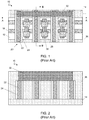
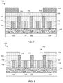
- FIG. 1 shows an example of a prior art IC structure 10 .
- FIG. 2 shows a cross-section of IC structure 10 taken along line A-A.
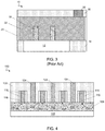
- FIG. 3 shows a cross-section of IC structure 10 taken along B-B.
- IC structure 10 may include a substrate 12 ( FIGS. 1 and 3 ) adjacent to a shallow trench isolation (STI) region 14 .
- a set of fins 18 ( FIGS. 1 and 3 ) may be formed form substrate 12 .
- Substantially surrounding fins 18 over portions of substrate 12 and STI region 14 may be gate stacks 20 .
- Gate stacks 20 may include a gate conductor 22 and gate spacers 24 .
- IC structure 10 may also include source/drain contacts 28 ( FIGS. 1 and 3 ) overlying portions of fins 18 to provide electrical connection to source/drain regions (not shown) therein.
- Source/drain contacts 28 may be adjacent to gate stacks 20 over substrate 12 and STI region 14 .
- IC structure 10 may also include a gate contact 32 .
- Gate contact 32 provides electrical connection to gate stacks 20 .
- IC structure 10 may also include a dielectric layer 36 over substrate 12 and STI region 14 .
- Dielectric layer 36 may substantially surround fins 18 , gate stacks 20 , source/drain contacts 28 , and gate contact 32 . In FIG. 1 , dielectric layer 36 is shown by phantom box in order to show features of IC structure 10 thereunder.
- IC structure 10 may also include one or more contacts 38 to source/drain contacts 28 .
- Contacts 38 may be disposed within dielectric layer 36 in the same plane as gate contact 32 .
- Contacts 38 provide electrical connection from source/drain contacts 28 to other structures and devices that may be formed in metal levels above dielectric layer 36 .
- gate contacts 32 are formed over gate stacks 20 over STI region 14 and not over gate stacks 20 in the active region, or over substrate 12 . Forming gate contacts 32 over STI region 14 results in a high gate resistance. Gate resistance is dependent in part on the length of gate stacks 20 and the distance of gate contact 32 to each end of gate stacks 20 . When gate contacts 32 are formed over STI region 14 , gate contacts 32 are closer to one end of gate stacks 32 than the other. Thus, an increase in gate resistance reduces the maximum oscillation frequency and RF cutoff frequency increases.
- a first aspect of the disclosure provides for a method of forming an integrated circuit structure.
- the method may include: lowering a height of a source/drain contact within a first dielectric layer to a height below a height of a gate conductor of a gate stack, the gate stack being adjacent to the gate conductor within the dielectric layer; and forming a conductor over and without contacting the source/drain contact, the conductor contacting the gate conductor.
- a second aspect of the disclosure provides for a method of forming and integrated circuit structure.
- the method may include: lowering a height of one or more source/drain contacts in a set of source/drain contacts below a height of a gate conductor within a gate stack of a set of gate stacks, the one or more source/drain contacts in the set of source/drain contacts being adjacent to the gate stack of the set of gate stacks within a first dielectric layer; and forming a conductor over and without contacting the set of source/drain contacts, the conductor contacting each gate conductor.
- a third aspect of the disclosure provides for an integrated circuit structure.
- the integrated circuit structure may include: a gate stack having a gate conductor therein over a substrate, the gate stack being within a dielectric layer; a source/drain contact to a source/drain region over the substrate and adjacent to the gate stack within the dielectric layer; an upper conductor extending above, without contacting, the source/drain contact, wherein the upper conductor extends within the dielectric layer to contact the gate conductor within the gate stack.
- a fourth aspect of the disclosure provides for an integrated circuit structure.
- the integrated circuit structure may include: a gate stack having a gate conductor therein over a substrate, the gate stack being within a first dielectric layer; a source/drain contact to a source/drain region over the substrate and adjacent to the gate stack within the first dielectric layer; an upper conductor extending above, and electrically isolated from, the source/drain contact, wherein the upper conductor extends within the first dielectric layer to contact the gate conductor within the gate stack; and a second dielectric layer separating the source/drain contact and the upper conductor.
- a fifth aspect of the disclosure provides for an integrated circuit structure.
- the integrated circuit structure may include: a gate stack having a gate conductor therein over a substrate, the gate stack being within a first dielectric layer; a source/drain contact to a source/drain region over the substrate and adjacent to the gate stack within the first dielectric layer; an upper conductor extending above, and electrically isolated from, the source/drain contact, wherein the upper conductor extends within the first dielectric layer to contact the gate conductor within the gate stack; a second dielectric layer separating the source/drain contact and the upper conductor; and an overlying contact positioned on a portion of the source/drain contact, wherein the overlying contact is planar with the upper conductor and electrically connects the source/drain contact to a metal level above the first dielectric layer, and wherein the portion of the source/drain contact is within the first dielectric layer and planar with a top surface of the first dielectric layer.
- FIG. 1 shows a top-down view of a prior art integrated circuit (IC) structure.
- FIG. 2 shows a cross-section of the prior art IC structure of FIG. 1 taken along line A-A.
- FIG. 3 shows a cross-section of the prior art IC structure of FIG. 1 taken along line B-B.
- FIGS. 4-9 show a cross-section of a preliminary IC structure undergoing aspects of a method according to embodiments of the disclosure with FIG. 9 showing a resulting IC structure.
- FIG. 10 shows a top-down view of an IC structure according to an embodiment of the disclosure.
- FIG. 11 shows a cross-section of the IC structure of FIG. 10 taken along line D-D.
- FIG. 12 shows a top-down view of an IC structure according to an embodiment of the disclosure.
- FIG. 13 shows a cross-section of the IC structure of FIG. 12 taken along line F-F.
- the present disclosure relates to an integrated circuit (IC) structure, and more particularly, to an integrated circuit structure having a gate contact and method of forming the same.
- Embodiments discussed herein provide a method of forming, and a corresponding structure, for a radiofrequency (RF) transistor having a reduced gate resistance.
- the IC structure as described herein includes a gate contact within the active region of the IC structure which causes a reduction in gate resistance. With the gate contact being located within active region, the gate contact is closer to each end of the gate stack than conventional gate contacts that are located over the STI region. The reduction of the gate resistance results in an increase in the maximum oscillation frequency (f max ) and a decrease in RF cutoff frequency (f T ).
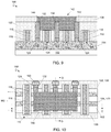
- FIGS. 4-9 show a cross-section of a preliminary IC structure undergoing aspects of a method according to embodiments of the disclosure, with FIG. 9 showing a resulting IC structure.
- IC structure 100 may be a fin-shaped field effect transistor (finFET) as shown.
- IC structure 100 may include a substrate 102 from which a fin 106 may be formed such that fin 106 is over substrate 102 .
- substrate 102 may include a semiconductor-on-insulator (SOI) substrate.
- SOI semiconductor-on-insulator
- substrate 102 may include a semiconductor layer, an insulator layer overlying the semiconductor layer, and another semiconductor layer overlying the insulator layer.
- An SOI substrate may be formed by depositing the insulator layer over the semiconductor layer and depositing another semiconductor layer over the insulator layer.
- the insulator layer may include silicon oxide (BOX layer) or other inorganic dielectric materials.
- a shallow trench isolation (STI) region may be disposed adjacent to substrate 102 as will be described herein.
- STI regions separate or isolate adjacent semiconductor devices that are on the same plane from one another. STI regions prevent electrical current leakage from the adjacent semiconductor devices.
- STI regions typically include an insulator, such as, for example, silicon dioxide.
- STI regions may be formed by etching portions of substrate 102 to form trenches therein, and filling the trenches, e.g., via depositing, with the insulator.
- the term “depositing” may include any now known or later developed technique appropriate for deposition, including but not limited to, for example: chemical vapor deposition (CVD), low-pressure CVD (LPCVD), plasma-enhanced CVD (PECVD), semi-atmosphere CVD (SACVD) high density plasma CVD (HDPCVD), rapid thermal CVD (RTCVD), ultra-high vacuum CVD (UHVCVD), limited reaction processing CVD (LRPCVD), metalorganic CVD (MOCVD), sputtering deposition, ion beam deposition, electron beam deposition, laser assisted deposition, thermal oxidation, thermal nitridation, spin-on methods, physical vapor deposition (PVD), atomic layer deposition (ALD), chemical oxidation, molecular beam epitaxy (MBE), plating, and evaporation.
- CVD chemical vapor deposition
- LPCVD low-pressure CVD
- PECVD plasma-enhanced CVD
- SACVD high
- Fin 106 maybe patterned and etched from the semiconductor layer overlying the insulator layer as is known in the art.
- substrate 102 may include a bulk silicon substrate from which fin 106 may be patterned and etched as is known in the art.
- IC structure 100 is shown and described as a finFET, it is to be understood that IC structure 100 may be any other type of transistor, e.g., a planar transistor, without departing from aspects of the disclosure.
- “Etching” generally refers to the removal of material from a substrate or structures formed on the substrate by wet or dry chemical means. In some instances, it may be desirable to selectively remove material from certain areas of the substrate. In such an instance, a mask may be used to prevent the removal of material from certain areas of the substrate.
- etching There are generally two categories of etching, (i) wet etch and (ii) dry etch. Wet etching may be used to selectively dissolve a given material and leave another material relatively intact. Wet etching is typically performed with a solvent, such as an acid. Dry etching may be performed using a plasma which may produce energetic free radicals, or species neutrally charged, that react or impinge at the surface of the wafer.
- Neutral particles may attack the wafer from all angles, and thus, this process is isotropic.
- Ion milling, or sputter etching bombards the wafer with energetic ions of noble gases from a single direction, and thus, this process is highly anisotropic.
- a reactive-ion etch (RIE) operates under conditions intermediate between sputter etching and plasma etching and may be used to produce deep, narrow features, such as trenches.
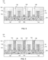
- Gate stacks 110 may substantially surround fin 106 over substrate 102 . While four gate stacks have been shown, any number of gate stacks may be formed over fin 106 without departing from aspects of the disclosure.
- Gate stacks 110 may each include a gate conductor 116 and gate spacers 118 substantially surrounding gate conductor 116 .
- Gate conductor 116 may include, for example, titanium, titanium nitride, tungsten, tungsten nitride, copper, copper nitride, tantalum, or tantalum nitride.
- gate stacks 110 may also include a gate dielectric (not shown) and work function metal layers (not shown) between fin 106 and gate conductor 116 . Further, overlying gate conductor 116 may be a gate cap layer (not shown).
- the gate dielectric may include, for example, at least one of: hafnium oxide, hafnium silicate, nitride hafnium silicate, zirconium oxide, zirconium silicate, titanium oxide, lanthanum oxide, yttrium oxide, aluminum oxide, or combinations thereof.
- the work function metal layers may act as a doping source, and a different work function setting metal can then be employed depending on whether an n-type field-effect-transistor (NFET) or a p-type field-effect-transistor (PFET) device is desired.
- NFET n-type field-effect-transistor
- PFET p-type field-effect-transistor
- the same gate conductor can be used in each of the devices, yet a different (if so desired) work function setting metal can be used in one or more devices to obtain a different doping polarity.
- suitable work function setting metals for use in PFET devices include, but are not limited to aluminum, dysprosium, gadolinium, and ytterbium.
- Suitable work function setting metals for use in NFET devices include, but are not limited to lanthanum, titanium, and tantalum.
- the gate cap layer may include, for example, at least one of: an oxide, e.g., silicon dioxide, or a nitride, e.g., silicon nitride.
- Gate spacers 118 may include, for example, at least one of: an oxide, e.g., silicon dioxide, or a nitride, e.g., silicon nitride.
- source/drain regions 112 may be formed from exposed portions of fins 106 , e.g., between gate stacks 110 .
- Source/drain regions 112 may be formed by doping, depositing, and/or epitaxial growth of semiconducting material on or around fins 106 .
- source/drain regions 112 may be formed by implanting n-type or p-type dopants directly into fin 106 .
- source/drain regions 112 may be formed by growth of an epitaxial material 172 from fins 106 such that epitaxial material 172 surrounds fins 106 as shown in the cross-sectional views of FIGS. 11 and 13 .
- Epitaxial material 172 may be chosen dependent on whether a PFET or an NFET is desired.
- silicon may be epitaxially grown and subsequently doped with an n-type dopant, e.g., carbon, such that epitaxial material includes carbon-doped silicon.
- silicon germanium may be epitaxially grown and subsequently doped with a p-type dopant, e.g., boron, such that epitaxial material includes boron-doped silicon germanium.
- epitaxial growth and/or deposition and “epitaxially formed and/or grown” mean the growth of a semiconductor material on a deposition surface of a semiconductor material, in which the semiconductor material being grown may have the same crystalline characteristics as the semiconductor material of the deposition surface.
- the chemical reactants provided by the source gases are controlled and the system parameters are set so that the depositing atoms arrive at the deposition surface of the semiconductor substrate with sufficient energy to move around on the surface and orient themselves to the crystal arrangement of the atoms of the deposition surface. Therefore, an epitaxial semiconductor material may have the same crystalline characteristics as the deposition surface on which it may be formed.
- an epitaxial semiconductor material deposited on a ⁇ 100 ⁇ crystal surface may take on a ⁇ 100 ⁇ orientation.
- epitaxial growth and/or deposition processes may be selective to forming on semiconductor surfaces, and may not deposit material on dielectric surfaces, such as silicon dioxide or silicon nitride surfaces.
- IC structure 100 may also include a dielectric layer 122 over fin 106 (including any epitaxial material surrounding fin 106 ) and substantially surrounding gate stacks 110 .
- Dielectric layer 122 may include, for example, silicon nitride, silicon oxide, fluorinated SiO 2 (FSG), hydrogenated silicon oxycarbide (SiCOH), porous SiCOH, boro-phospho-silicate glass (BPSG), silsesquioxanes, carbon doped oxides (i.e., organosilicates) that include atoms of silicon, carbon, oxygen, and/or hydrogen, thermosetting polyarylene ethers, SiLK (a polyarylene ether available from Dow Chemical Corporation), a spin-on silicon-carbon containing polymer material available from JSR Corporation, other low dielectric constant ( ⁇ 3.9) material, or layers thereof.
- Dielectric layer 122 may be formed by deposition of dielectric layer material.
- IC structure 100 may also include source/drain contacts 124 .
- Source/drain contacts 124 may be formed by forming a mask (not shown), patterning the mask, and etching an opening (not shown) within dielectric layer 122 to expose source/drain regions 112 of fin 106 (including any source/drain region 112 formed from any epitaxial material surrounding fin 106 ).
- Source/drain contacts 124 may be formed within the opening.
- Source/drain contacts 124 may contact source/drain region 112 and provide electrical connect thereto.
- Source/drain contacts 124 may be formed by depositing a liner layer, e.g., titanium, and a metallization layer within the opening to fill the opening.
- the process may include annealing source/drain regions 112 at the bottom of the opening to create a silicide (not shown) therein, i.e., silicon metal alloy, thereby creating a surface for the contact connection.
- a silicide i.e., silicon metal alloy
- the silicide that is formed in aforementioned manner may be called liner silicide.
- Source/drain contact 124 may be planarized to a top surface of dielectric layer 122 .
- Planarization refers to various processes that make a surface more planar (that is, more flat and/or smooth).
- Chemical-mechanical-polishing is one currently conventional planarization process which planarizes surfaces with a combination of chemical reactions and mechanical forces.
- planarization techniques may include: (i) oxidation; (ii) chemical etching; (iii) taper control by ion implant damage; (iv) deposition of films of low-melting point glass; (v) resputtering of deposited films to smooth them out; (vi) photosensitive polyimide (PSPI) films; (vii) new resins; (viii) low-viscosity liquid epoxies; (ix) spin-on glass (SOG) materials; and/or (x) sacrificial etch-back.
- PSPI photosensitive polyimide
- a “mask” is a material or stack of materials which may be formed over an underlying material which is to be processed.
- the mask may be patterned to have openings such that the underlying material is exposed. Subsequently, the underlying material may be processed where the underlying material is exposed by the openings in the mask. Once the underlying material is processed, the mask may be removed.
- Conventional masking materials include photoresist, silicon oxide, amorphous carbon, spin-on materials and silicon nitride.
- source/drain contacts 124 may be recessed to create openings 128 within dielectric layer 122 over source/drain contacts 124 . That is, a height of source/drain contacts 124 may be lowered to a height that is below a height of gate conductor 116 of each gate stack 110 .
- Source/drain contacts 124 may be recessed by etching, e.g., RIE.
- Source/drain contacts 124 may be etched such that a portion of source/drain contacts 124 remain over source/drain regions 112 within fin 106 .
- an insulating layer 132 may be formed within openings 128 over the recessed source/drain contacts 124 .
- Insulating layer 132 may include a layer having a low dielectric constant (low-k dielectric layer).
- Low-k dielectric layer may include, for example, silicon nitride, silicon oxide, fluorinated SiO 2 (FSG), hydrogenated silicon oxycarbide (SiCOH), porous SiCOH, boro-phospho-silicate glass (BPSG), silsesquioxanes, carbon doped oxides (i.e., organosilicates) that include atoms of silicon, carbon, oxygen, and/or hydrogen, thermosetting polyarylene ethers, SiLK (a polyarylene ether available from Dow Chemical Corporation), a spin-on silicon-carbon containing polymer material available from JSR Corporation, other low dielectric constant ( ⁇ 3.9) material, or layers thereof. Insulating layer 132 may then be formed by depositing insulating layer material within opening(s) 128 and planarizing the insulating layer material to a top surface of dielectric layer 122 .
- FSG fluorinated SiO 2
- dielectric layer 136 may be formed, e.g., deposited, over dielectric layer 122 and insulating layer 132 .
- Dielectric layer 136 may include any of the materials discussed with respect to dielectric layer 122 such that dielectric layer 136 and dielectric layer 122 may, in one instance, be of the same material or composition.
- a mask 138 may be formed, e.g., deposited, over dielectric layer 136 .
- Mask 138 may be patterned and etched to expose a portion of dielectric layer 136 where it is desired for dielectric layer 136 to be etched.
- the exposed portions of dielectric layer 136 may be removed, e.g., via etching (RIE).
- RIE etching
- the etching may continue through dielectric layer 122 until top portions of gate conductor 116 of any underlying gate stack 110 are exposed by an opening 142 .
- Opening 142 may also expose portions of insulating layer 132 .
- the gate cap layer may also be removed, e.g., via etching, to expose gate conductor 116 thereunder.
- a conductor 146 may be formed within opening 142 such that conductor 146 is formed over, and without contacting, source/drain contacts 124 .
- Conductor 146 may be formed such that conductor 146 contacts gate conductor 116 and portions of low-k dielectric layer 132 .
- Conductor 146 may be a gate contact providing electrical connection to gate stacks 110 thereunder.
- Conductor 146 may include, for example, tungsten, cobalt, or copper.
- Conductor 146 may be planarized to a top surface of dielectric layer 136 .
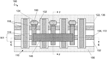
- the resulting IC structure 190 after planarization may include gate stack 110 having gate conductor 116 therein over substrate 102 .
- Gate stack 110 may be within dielectric layer 122 .
- IC structure 190 may also include source/drain contact 124 to a source/drain region 112 over substrate 102 and adjacent to gate stack 110 within dielectric layer 122 .
- insulating layer 132 may be disposed within opening 128 ( FIGS. 2-3 ) over source/drain contact 124 within dielectric layer 122 and separate source/drain contact 124 and conductor 146 .
- portions of insulating layer 132 may be disposed within dielectric layer 136 .
- Conductor 146 may extend over at least a portion of the insulating layer 132 and extend within portions of dielectric layers 122 , 136 to contact gate conductor 116 within the gate stack 110 .
- processes of the disclosure as described herein may be customized based on desired application of IC structure 190 . That is, the forming the patterning and etching of mask 138 ( FIG. 7 ) to form opening 142 ( FIGS. 8-9 ) may be customized and/or modified to result in opening 142 having any desired configuration to expose portions of gate conductors 116 of gate stacks 110 and low-k dielectric layers 132 thereunder.
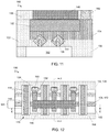
- FIG. 10 shows a top-down view of IC structure 190 according to one embodiment of the disclosure wherein the embodiments described with respect to FIGS. 4-9 show cross-sections taken along line C-C of FIG. 10 .
- FIG. 11 shows a cross-section of IC structure 190 taken along line D-D of FIG. 10 .
- dielectric layers 122 , 136 are shown as a phantom box in FIG. 10 such that features of IC structure 190 thereunder can be seen.
- conductor 146 may be formed within dielectric layers 122 , 136 over one or more gate stacks 110 ( FIG. 10 ) and low-k dielectric layer 132 substantially within the active region of IC structure 190 , or over substrate 102 , as opposed to substantially over STI region 156 that is adjacent to substrate 102 . That is, conductor 146 formed herein is closer to each end of gate stacks 110 than conventional gate contacts over STI region 156 . Such a feature results in a reduction of gate resistance and an increase in the maximum oscillation frequency.
- source/drain contacts 124 may contact epitaxial material 172 surrounding fin 106 .
- source/drain contact 124 may contact fin 106 directly where fin 106 was doped to form source/drain regions 112 ( FIG. 9 ) within fin 106 .
- a portion of source/drain contact 124 over STI region 156 may not have been recessed as was described with respect to FIG. 5 .
- the lithographic process used to recess source/drain contact 124 may include covering portions of source/drain contact 124 over STI region 156 with the mask such that the portions of source/drain contact 124 over STI region 156 are not etched or recessed.
- the portions of source/drain contact 124 over STI region 156 may extend from within dielectric layer 122 to a top surface of dielectric layer 122 such that a top surface of those portions of source/drain contact 124 are substantially planar with a top surface of low-k dielectric layer 132 that is over the portions of the recessed source/drain contact 124 .
- contacts 160 to source/drain contacts 124 may be formed over the portions of source/drain contact 124 that was not recessed, or portions of source/drain contact 124 over STI region 156 .
- Contacts 160 may be formed within dielectric layer 136 such that contacts 160 are within the same plane as conductor 146 .
- Contacts 160 may formed within dielectric layer 136 by conventional lithographic techniques, e.g., masking, patterning, etching, depositing, and planarizing.
- Contacts 160 may include a conductive metal such as any of the conductive metals discussed herein and may be formed simultaneously with the formation of conductor 146 . In other embodiments, contacts 160 may be formed before or after the formation of conductor 146 .
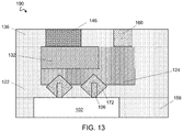
- FIGS. 12-13 show another example of IC structure 190 according to embodiments of the disclosure.
- FIG. 12 shows a top-down view of IC structure 190 according to one embodiment of the disclosure wherein the embodiments described with respect to FIGS. 4-9 show cross-sections taken along line E-E of FIG. 12 .
- FIG. 13 shows a cross-section of IC structure 190 taken along line F-F of FIG. 12 .
- dielectric layers 122 , 136 are shown as a phantom box in FIG. 12 such that features of IC structure 190 thereunder can be seen.
- conductor 146 may be formed within dielectric layers 122 , 136 over one or more gate stacks 110 ( FIG. 12 ) and over low-k dielectric layer 132 substantially within the active region of IC structure 190 , or over substrate 102 , as opposed to substantially over STI region 156 that is adjacent to substrate 102 . Such a feature results in a reduction of gate resistance and an increase in the maximum oscillation frequency.
- source/drain contact 124 may contact epitaxial material 172 surrounding fin 106 .
- source/drain contact 124 may contact fin 106 directly where fin 106 was doped to form source/drain regions 112 ( FIG. 9 ) within fin 106 .
- a portion of source/drain contact 124 over STI region 156 may not have been recessed as was described with respect to FIG. 5 .
- the lithographic process used to recess source/drain contact 124 may include covering portions of source/drain contact 124 over STI region 156 with the mask such that the portions of source/drain contact 124 over STI region 156 are not etched or recessed.
- the portions of source/drain contact 124 over STI region 156 may extend from within dielectric layer 122 to a top surface of dielectric layer 122 such that a top surface of those portions of source/drain contact 124 are substantially planar with a top surface of low-k dielectric layer 132 that is over the portions of the recessed source/drain contact 124 .
- the unrecessed portion of source/drain contact 124 may straddle a portion of substrate 102 and STI region 156 .
- This embodiment may differ from the embodiment shown in FIGS. 10-11 in that conductor 146 has a width W 1 ( FIG. 12 ) that is substantially smaller than a width W 2 ( FIG. 10 ) of conductor 146 described with respect to FIGS. 10-11 .
- contacts 160 to source/drain contacts 124 may be formed over the portions of source/drain contact 124 that was not recessed, or portions of source/drain contact 124 over STI region 156 .
- Contacts 160 may be formed within dielectric layer 136 such that contacts 160 are within the same plane as conductor 146 .
- Contacts 160 may formed within dielectric layer 136 by conventional lithographic techniques, e.g., masking, patterning, etching, depositing, and planarizing.
- Contacts 160 may include a conductive metal such as any of the conductive metals discussed herein and may be formed simultaneously with the formation of conductor 146 . In other embodiments, contacts 160 may be formed before or after the formation of conductor 146 .
- the methods as described above are used in the fabrication of integrated circuit chips.
- the resulting integrated circuit chips can be distributed by the fabricator in raw wafer form (that is, as a single wafer that has multiple unpackaged chips), as a bare die, or in a packaged form.
- the chip is mounted in a single chip package (such as a plastic carrier, with leads that are affixed to a motherboard or other higher level carrier) or in a multichip package (such as a ceramic carrier that has either or both surface interconnections or buried interconnections).
- the chip is then integrated with other chips, discrete circuit elements, and/or other signal processing devices as part of either (a) an intermediate product, such as a motherboard, or (b) an end product.
- the end product can be any product that includes integrated circuit chips, ranging from toys and other low-end applications to advanced computer products having a display, a keyboard or other input device, and a central processor.
Landscapes
- Insulated Gate Type Field-Effect Transistor (AREA)
- Electrodes Of Semiconductors (AREA)
- Thin Film Transistor (AREA)
Abstract
Description
Claims (20)
Priority Applications (1)
| Application Number | Priority Date | Filing Date | Title |
|---|---|---|---|
| US16/122,259 US10629532B2 (en) | 2016-07-11 | 2018-09-05 | Integrated circuit structure having gate contact and method of forming same |
Applications Claiming Priority (2)
| Application Number | Priority Date | Filing Date | Title |
|---|---|---|---|
| US15/206,361 US10128187B2 (en) | 2016-07-11 | 2016-07-11 | Integrated circuit structure having gate contact and method of forming same |
| US16/122,259 US10629532B2 (en) | 2016-07-11 | 2018-09-05 | Integrated circuit structure having gate contact and method of forming same |
Related Parent Applications (1)
| Application Number | Title | Priority Date | Filing Date |
|---|---|---|---|
| US15/206,361 Division US10128187B2 (en) | 2016-07-11 | 2016-07-11 | Integrated circuit structure having gate contact and method of forming same |
Publications (2)
| Publication Number | Publication Date |
|---|---|
| US20190006280A1 US20190006280A1 (en) | 2019-01-03 |
| US10629532B2 true US10629532B2 (en) | 2020-04-21 |
Family
ID=60911220
Family Applications (2)
| Application Number | Title | Priority Date | Filing Date |
|---|---|---|---|
| US15/206,361 Active 2036-08-26 US10128187B2 (en) | 2016-07-11 | 2016-07-11 | Integrated circuit structure having gate contact and method of forming same |
| US16/122,259 Active US10629532B2 (en) | 2016-07-11 | 2018-09-05 | Integrated circuit structure having gate contact and method of forming same |
Family Applications Before (1)
| Application Number | Title | Priority Date | Filing Date |
|---|---|---|---|
| US15/206,361 Active 2036-08-26 US10128187B2 (en) | 2016-07-11 | 2016-07-11 | Integrated circuit structure having gate contact and method of forming same |
Country Status (3)
| Country | Link |
|---|---|
| US (2) | US10128187B2 (en) |
| CN (1) | CN107611088B (en) |
| TW (1) | TWI648818B (en) |
Families Citing this family (9)
| Publication number | Priority date | Publication date | Assignee | Title |
|---|---|---|---|---|
| WO2018182611A1 (en) * | 2017-03-30 | 2018-10-04 | Intel Corporation | Back side processing of integrated circuit structures to form insulation structure between adjacent transistor structures |
| US10177037B2 (en) * | 2017-04-25 | 2019-01-08 | Globalfoundries Inc. | Methods of forming a CT pillar between gate structures in a semiconductor |
| KR102529229B1 (en) | 2018-06-07 | 2023-05-04 | 삼성전자주식회사 | A semiconductor device |
| US10811319B2 (en) * | 2018-11-29 | 2020-10-20 | Globalfoundries Inc. | Middle of line structures |
| KR102491555B1 (en) | 2018-11-30 | 2023-01-20 | 삼성전자주식회사 | Semiconductor device and method for fabricating the same |
| KR102788489B1 (en) | 2019-08-30 | 2025-03-28 | 삼성전자주식회사 | Semiconductor device and method for fabricating the same |
| KR102820465B1 (en) * | 2019-09-17 | 2025-06-17 | 삼성전자주식회사 | Semiconductor devices and methods of manufacturing semiconductor devices |
| KR102824742B1 (en) * | 2020-09-16 | 2025-06-24 | 삼성전자주식회사 | Integrated circuit devices |
| KR102876972B1 (en) | 2021-06-01 | 2025-10-29 | 삼성전자주식회사 | Semiconductor device |
Citations (10)
| Publication number | Priority date | Publication date | Assignee | Title |
|---|---|---|---|---|
| US6239491B1 (en) | 1998-05-18 | 2001-05-29 | Lsi Logic Corporation | Integrated circuit structure with thin dielectric between at least local interconnect level and first metal interconnect level, and process for making same |
| CN1540767A (en) | 2003-04-24 | 2004-10-27 | �����ɷ� | field effect transistor |
| US20070069307A1 (en) | 2005-09-27 | 2007-03-29 | Kentaro Eda | Semiconductor device and method of manufacturing the same |
| US20090014796A1 (en) * | 2007-07-09 | 2009-01-15 | Jhon-Jhy Liaw | Semiconductor Device with Improved Contact Structure and Method of Forming Same |
| US20130264639A1 (en) | 2010-12-21 | 2013-10-10 | Glenn A. Glass | Column iv transistors for pmos integration |
| US20140001520A1 (en) | 2012-06-29 | 2014-01-02 | Glenn A. Glass | Contact resistance reduced p-mos transistors employing ge-rich contact layer |
| CN104253079A (en) | 2013-06-25 | 2014-12-31 | 中国科学院微电子研究所 | Shallow trench isolation structure, transistor including same and manufacturing method thereof |
| US20150380558A1 (en) | 2014-06-30 | 2015-12-31 | Taiwan Semiconductor Manufacturing Company, Ltd. | Finfet thermal protection methods and related structures |
| US20160141423A1 (en) | 2014-11-18 | 2016-05-19 | Taiwan Semiconductor Manufacturing Company, Ltd. | Contacts For Highly Scaled Transistors |
| US20160197071A1 (en) | 2015-01-06 | 2016-07-07 | Mediatek Inc. | Integrated circuit device and method for forming the same |
-
2016
- 2016-07-11 US US15/206,361 patent/US10128187B2/en active Active
-
2017
- 2017-05-25 TW TW106117386A patent/TWI648818B/en not_active IP Right Cessation
- 2017-07-11 CN CN201710559802.XA patent/CN107611088B/en active Active
-
2018
- 2018-09-05 US US16/122,259 patent/US10629532B2/en active Active
Patent Citations (11)
| Publication number | Priority date | Publication date | Assignee | Title |
|---|---|---|---|---|
| US6239491B1 (en) | 1998-05-18 | 2001-05-29 | Lsi Logic Corporation | Integrated circuit structure with thin dielectric between at least local interconnect level and first metal interconnect level, and process for making same |
| CN1540767A (en) | 2003-04-24 | 2004-10-27 | �����ɷ� | field effect transistor |
| US7009263B2 (en) | 2003-04-24 | 2006-03-07 | Infineon Technologies Ag | Field-effect transistor |
| US20070069307A1 (en) | 2005-09-27 | 2007-03-29 | Kentaro Eda | Semiconductor device and method of manufacturing the same |
| US20090014796A1 (en) * | 2007-07-09 | 2009-01-15 | Jhon-Jhy Liaw | Semiconductor Device with Improved Contact Structure and Method of Forming Same |
| US20130264639A1 (en) | 2010-12-21 | 2013-10-10 | Glenn A. Glass | Column iv transistors for pmos integration |
| US20140001520A1 (en) | 2012-06-29 | 2014-01-02 | Glenn A. Glass | Contact resistance reduced p-mos transistors employing ge-rich contact layer |
| CN104253079A (en) | 2013-06-25 | 2014-12-31 | 中国科学院微电子研究所 | Shallow trench isolation structure, transistor including same and manufacturing method thereof |
| US20150380558A1 (en) | 2014-06-30 | 2015-12-31 | Taiwan Semiconductor Manufacturing Company, Ltd. | Finfet thermal protection methods and related structures |
| US20160141423A1 (en) | 2014-11-18 | 2016-05-19 | Taiwan Semiconductor Manufacturing Company, Ltd. | Contacts For Highly Scaled Transistors |
| US20160197071A1 (en) | 2015-01-06 | 2016-07-07 | Mediatek Inc. | Integrated circuit device and method for forming the same |
Non-Patent Citations (3)
| Title |
|---|
| Taiwanese Office Action and English Translation thereof for TW Patent Application No. 106117386 dated Jun. 11, 2018, 9 pages. |
| U.S. Appl. No. 15/206,361 Office Action dated Oct. 5, 2017, 9 pages. |
| U.S. Appl. No. 15/206,361, Notice of Allowance dated Jul. 5, 2018, 7 pages. |
Also Published As
| Publication number | Publication date |
|---|---|
| US20190006280A1 (en) | 2019-01-03 |
| US20180012839A1 (en) | 2018-01-11 |
| US10128187B2 (en) | 2018-11-13 |
| CN107611088A (en) | 2018-01-19 |
| TWI648818B (en) | 2019-01-21 |
| CN107611088B (en) | 2020-08-18 |
| TW201812997A (en) | 2018-04-01 |
Similar Documents
| Publication | Publication Date | Title |
|---|---|---|
| US10629532B2 (en) | Integrated circuit structure having gate contact and method of forming same | |
| US10256235B2 (en) | Vertical transistors and methods of forming same | |
| US9786765B2 (en) | FINFET having notched fins and method of forming same | |
| US10049985B2 (en) | Contact line having insulating spacer therein and method of forming same | |
| US9917103B1 (en) | Diffusion break forming after source/drain forming and related IC structure | |
| US10157794B1 (en) | Integrated circuit structure with stepped epitaxial region | |
| US10090169B1 (en) | Methods of forming integrated circuit structures including opening filled with insulator in metal gate | |
| US11482456B2 (en) | Forming two portion spacer after metal gate and contact formation, and related IC structure | |
| US10090204B1 (en) | Vertical FINFET structure and methods of forming same | |
| US10121893B2 (en) | Integrated circuit structure without gate contact and method of forming same | |
| US9991167B2 (en) | Method and IC structure for increasing pitch between gates | |
| US11094834B2 (en) | Junction field effect transistor (JFET) structure and methods to form same | |
| US9583397B1 (en) | Source/drain terminal contact and method of forming same | |
| US11217584B2 (en) | Limiting lateral epitaxy growth at N-P boundary using inner spacer, and related structure | |
| EP4243083A1 (en) | Bipolar transistor structures with base having varying horizontal width and methods to form same | |
| CN114927568B (en) | Integrated circuit structure and method for bipolar transistors having an outer base aligned with the gate of a FET | |
| US20250248088A1 (en) | Gate structure on intrinsic base layer and overhanging lateral sidewall of intrinsic base layer | |
| US11784224B2 (en) | Lateral bipolar transistor structure with base over semiconductor buffer and related method | |
| US20190131424A1 (en) | Methods for forming ic structure having recessed gate spacers and related ic structures | |
| US20190393077A1 (en) | Method of forming semiconductor material in trenches having different widths, and related structures | |
| US20250241062A1 (en) | Structure with two work function metals over conductive bridge, and method to form same | |
| US20250254985A1 (en) | Finfet with gate-all-around structure including gate dielectric layer thicker in buried gate region than in outer gate region | |
| US11152394B1 (en) | Structure with polycrystalline isolation region below polycrystalline fill shape(s) and selective active device(s), and related method | |
| US11545575B2 (en) | IC structure with fin having subfin extents with different lateral dimensions |
Legal Events
| Date | Code | Title | Description |
|---|---|---|---|
| AS | Assignment |
Owner name: GLOBALFOUNDRIES INC., CAYMAN ISLANDS Free format text: ASSIGNMENT OF ASSIGNORS INTEREST;ASSIGNORS:ZANG, HUI;WATTS, JOSEF S.;REEL/FRAME:046792/0552 Effective date: 20160708 |
|
| FEPP | Fee payment procedure |
Free format text: ENTITY STATUS SET TO UNDISCOUNTED (ORIGINAL EVENT CODE: BIG.); ENTITY STATUS OF PATENT OWNER: LARGE ENTITY |
|
| STPP | Information on status: patent application and granting procedure in general |
Free format text: APPLICATION DISPATCHED FROM PREEXAM, NOT YET DOCKETED |
|
| STPP | Information on status: patent application and granting procedure in general |
Free format text: DOCKETED NEW CASE - READY FOR EXAMINATION |
|
| STPP | Information on status: patent application and granting procedure in general |
Free format text: NON FINAL ACTION MAILED |
|
| STPP | Information on status: patent application and granting procedure in general |
Free format text: RESPONSE TO NON-FINAL OFFICE ACTION ENTERED AND FORWARDED TO EXAMINER |
|
| STPP | Information on status: patent application and granting procedure in general |
Free format text: NOTICE OF ALLOWANCE MAILED -- APPLICATION RECEIVED IN OFFICE OF PUBLICATIONS |
|
| STPP | Information on status: patent application and granting procedure in general |
Free format text: NOTICE OF ALLOWANCE MAILED -- APPLICATION RECEIVED IN OFFICE OF PUBLICATIONS |
|
| STCF | Information on status: patent grant |
Free format text: PATENTED CASE |
|
| AS | Assignment |
Owner name: GLOBALFOUNDRIES U.S. INC., CALIFORNIA Free format text: ASSIGNMENT OF ASSIGNORS INTEREST;ASSIGNOR:GLOBALFOUNDRIES INC.;REEL/FRAME:054633/0001 Effective date: 20201022 |
|
| AS | Assignment |
Owner name: GLOBALFOUNDRIES U.S. INC., NEW YORK Free format text: RELEASE BY SECURED PARTY;ASSIGNOR:WILMINGTON TRUST, NATIONAL ASSOCIATION;REEL/FRAME:056987/0001 Effective date: 20201117 Owner name: GLOBALFOUNDRIES U.S. INC., NEW YORK Free format text: RELEASE OF SECURITY INTEREST;ASSIGNOR:WILMINGTON TRUST, NATIONAL ASSOCIATION;REEL/FRAME:056987/0001 Effective date: 20201117 |
|
| MAFP | Maintenance fee payment |
Free format text: PAYMENT OF MAINTENANCE FEE, 4TH YEAR, LARGE ENTITY (ORIGINAL EVENT CODE: M1551); ENTITY STATUS OF PATENT OWNER: LARGE ENTITY Year of fee payment: 4 |