US9830260B2 - Method for mapping page address based on flash memory and system therefor - Google Patents
Method for mapping page address based on flash memory and system therefor Download PDFInfo
- Publication number
- US9830260B2 US9830260B2 US14/779,954 US201314779954A US9830260B2 US 9830260 B2 US9830260 B2 US 9830260B2 US 201314779954 A US201314779954 A US 201314779954A US 9830260 B2 US9830260 B2 US 9830260B2
- Authority
- US
- United States
- Prior art keywords
- addresses
- mapping
- logical
- mapping information
- flash memory
- Prior art date
- Legal status (The legal status is an assumption and is not a legal conclusion. Google has not performed a legal analysis and makes no representation as to the accuracy of the status listed.)
- Active
Links
Images


Classifications
-
- G—PHYSICS
- G06—COMPUTING; CALCULATING OR COUNTING
- G06F—ELECTRIC DIGITAL DATA PROCESSING
- G06F12/00—Accessing, addressing or allocating within memory systems or architectures
- G06F12/02—Addressing or allocation; Relocation
-
- G—PHYSICS
- G06—COMPUTING; CALCULATING OR COUNTING
- G06F—ELECTRIC DIGITAL DATA PROCESSING
- G06F12/00—Accessing, addressing or allocating within memory systems or architectures
- G06F12/02—Addressing or allocation; Relocation
- G06F12/0223—User address space allocation, e.g. contiguous or non contiguous base addressing
- G06F12/0292—User address space allocation, e.g. contiguous or non contiguous base addressing using tables or multilevel address translation means
-
- G—PHYSICS
- G06—COMPUTING; CALCULATING OR COUNTING
- G06F—ELECTRIC DIGITAL DATA PROCESSING
- G06F12/00—Accessing, addressing or allocating within memory systems or architectures
- G06F12/02—Addressing or allocation; Relocation
- G06F12/0223—User address space allocation, e.g. contiguous or non contiguous base addressing
- G06F12/023—Free address space management
- G06F12/0238—Memory management in non-volatile memory, e.g. resistive RAM or ferroelectric memory
- G06F12/0246—Memory management in non-volatile memory, e.g. resistive RAM or ferroelectric memory in block erasable memory, e.g. flash memory
-
- G—PHYSICS
- G06—COMPUTING; CALCULATING OR COUNTING
- G06F—ELECTRIC DIGITAL DATA PROCESSING
- G06F2212/00—Indexing scheme relating to accessing, addressing or allocation within memory systems or architectures
- G06F2212/10—Providing a specific technical effect
- G06F2212/1016—Performance improvement
- G06F2212/1024—Latency reduction
-
- G—PHYSICS
- G06—COMPUTING; CALCULATING OR COUNTING
- G06F—ELECTRIC DIGITAL DATA PROCESSING
- G06F2212/00—Indexing scheme relating to accessing, addressing or allocation within memory systems or architectures
- G06F2212/20—Employing a main memory using a specific memory technology
- G06F2212/202—Non-volatile memory
- G06F2212/2022—Flash memory
-
- G—PHYSICS
- G06—COMPUTING; CALCULATING OR COUNTING
- G06F—ELECTRIC DIGITAL DATA PROCESSING
- G06F2212/00—Indexing scheme relating to accessing, addressing or allocation within memory systems or architectures
- G06F2212/72—Details relating to flash memory management
- G06F2212/7201—Logical to physical mapping or translation of blocks or pages
Definitions
- the present invention relates to a method and system for page-level address mapping based on flash memory. More particularly, the present invention relates to a system and method for improving performance when a system is being booted.
- a Flash Translation Layer is present between a file system and flash memory in order to perform the file system's requirement for accessing a system based on NAND flash memory. Because a general file system is designed based on a hard disk, the cost of a read operation is the same as the cost of a write operation and data can be overwritten. However, in the case of a flash memory-based system, the costs of a read operation, a write operation, and an erase operation are different, data cannot be overwritten, and flash memory has erase-before-write constraints. Therefore, for smooth operations when an Operating System (OS) or a file system accesses a flash memory-based system, a flash translation layer executes functions of mapping addresses between flash memory and the OS or the file system and maintaining the mapping information.
- OS Operating System
- a flash translation layer executes functions of mapping addresses between flash memory and the OS or the file system and maintaining the mapping information.
- An FTL translates a request for a logical sector from a file system into a physical page of flash memory. If updates occur in the flash memory, the FTL writes data for the requested sector to a newly allocated block, and then modifies mapping information of a mapping table. Also, the FTL provides a wear-leveling function for a limited block erase count of flash memory.
- mapping methods for FTL algorithms there are page mapping, block mapping, and hybrid mapping.
- Page mapping maintains mapping information for the whole area of flash memory by a page unit.
- a page mapping table is in memory (DRAM or SDRAM), or a part of the page mapping table may be cached in the memory.
- the page mapping is advantageous in writing data to flash memory through a random write access pattern, but has a disadvantage in that it requires much memory for the page mapping table.
- Block mapping requires a small size for mapping information, but when write operations with a fixed offset occur frequently in response to repeated requests, performance may be degraded because of the increased number of merge operations.
- Hybrid mapping considers the advantages and disadvantages of the two mapping methods mentioned above.
- Hybrid mapping is flexible in a random write access pattern as the size of a page mapping area increases, but requires cost for searching a hybrid area when reading or writing the mapping information is requested. Also, time overhead occurs in finding an offset in a block. Therefore, the existing flash translation layer may degrade the performance of a system.
- Korean Patent Application Publication No. 10-2012-0074707 titled “Flash memory based storage and method for address mapping and data allocation thereof”, discloses a method for effectively managing address mapping and data page allocation for a storage device using flash memory.
- the above conventional art applies different address mapping methods according to data write access patterns, and differently allocates the physical location of flash memory according to the write patterns, whereby the cost for garbage collection in a data area is reduced and the life of flash memory may be extended.
- An object of the present invention is to condense mapping information concerning a write operation by using the sequential features of logical addresses and a data size.
- Another object of the present invention is to decrease the number of read operations by storing a page mapping table of which the size is reduced in DRAM rather than simply storing a page mapping table remaining intact in DRAM.
- the present invention intends to improve the boot performance of a flash memory-based system by reducing time that it takes to read booting information by storing condensed mapping information in memory of FTL, such as DRAM and/or SRAM.
- a system for a page-level address mapping based on flash memory may include a processor and a FTL memory (memory within a flash translation layer).
- the processor may include a write operation reception unit, a condensed mapping information generation unit, a mapping information storage management unit, a read operation reception unit, a search unit, a calculation unit, and a read operation unit.
- a system for a page-level address mapping based on flash memory may include a processor.
- the processor may include a mapping information querying unit, a detection unit, and a mapping information management unit.
- the write operation reception unit receives a write operation from a file system, and the condensed mapping information generation unit generates condensed mapping information, using the data size of the write operation and the start logical address of sequentially allocated logical addresses of the write operation.
- the FTL memory stores the condensed mapping information as an FTL mapping table.
- the mapping information storage management unit may store a flash memory mapping table including the start logical address, a start physical address corresponding to the start logical address, and the data size of the write operation, calculated by a page unit, in the system area of the flash memory.
- the mapping information storage management unit may store the condensed form of flash memory mapping table in the system area of the flash memory.
- the flash memory mapping table may be reconstructed into a table having mapping information for each page, and the reconstructed table may be stored in the system area of the flash memory.
- the mapping information storage management unit may store a flash memory mapping table including one-to-one mapping information between logical page addresses and physical page addresses in the system area of the flash memory.
- the read operation reception unit receives a read operation from the file system, and the search unit searches the FTL mapping table for a start logical address, which is identical to the logical address requested by the read operation or is the closest to and smaller than the logical address requested by the read operation.
- the calculation unit calculates a physical address corresponding to the read operation using the found start logical address and the logical address requested by the read operation.
- the read operation unit reads data stored at the calculated physical address of the flash memory.
- the mapping information querying unit may query the flash memory mapping table for mapping information between logical addresses and physical addresses by executing a read operation on the system area of the flash memory when a main computing system is booted, and the detection unit detects sequential logical addresses and sequential physical addresses corresponding to the sequential logical addresses, based on the found mapping information.
- the mapping information management unit condenses the mapping information of the flash memory, which includes a start logical address, a start physical address corresponding to the start logical address, and the size of sequential data; and then stores the condensed information in the memory of the flash translation layer.
- the mapping information management unit determines whether the logical addresses and physical addresses of the current entry and the next entry of the flash memory mapping table are sequential. If the logical addresses and physical addresses of the current entry and the next entry are sequential, the current entry and the next entry are condensed into a single entry, and the mapping information generated by the condensing process may be stored in the memory of the flash translation layer.
- a flash memory-based page-level address mapping method includes a step for receiving a write operation, a step for generating condensed mapping information, a step for storing mapping information in the memory of a flash translation layer, and a step for storing mapping information in the system area of flash memory.
- a write operation is received from a file system.
- condensed mapping information is generated using the data size of the write operation and the start logical address of sequentially allocated logical addresses of the write operation.
- mapping information in the memory of a flash translation layer the condensed mapping information including the start logical address, a start physical address corresponding to the start logical address, and the data size of the write operation, calculated by a page unit, are stored as an FTL mapping table in the memory of the flash translation layer.
- a flash memory mapping table including the start logical address, a start physical address corresponding to the start logical address, and the data size of the write operation, calculated by a page unit, is stored in the flash memory.
- a flash memory mapping table including one-to-one mapping information between logical page addresses and physical page addresses may be stored in the flash memory, based on the FTL mapping table.
- the flash memory-based page-level address mapping method further includes: a step for receiving a read operation from the file system; a step for searching the FTL mapping table for a start logical address, which is identical to the logical address requested by the read operation or is the closest to and smaller than the logical address requested by the read operation; a step for calculating a physical address corresponding to the read operation, using the found start logical address and the logical address requested by the read operation; and a step for reading data stored at the calculated physical address of the flash memory.
- a flash memory-based page-level address mapping method includes: a step for querying mapping information between the logical addresses and the physical addresses stored in the flash memory by executing a read operation on the system area of the flash memory when a main computing system is booted; a step for detecting sequential logical addresses and sequential physical addresses corresponding to the sequential logical addresses, based on the found mapping information; and a step for storing mapping information including a start logical address, a start physical address corresponding to the start logical address, and the size of sequential data in the memory of the flash translation layer, the mapping information being condensed using the sizes indicated by the detected sequential logical addresses and the detected sequential physical addresses.
- mapping information in the memory of the flash translation layer, if the logical addresses and physical addresses of the current entry and the next entry are sequential, the FTL mapping information in which the current entry and the next entry are condensed into a single entry is stored in the memory of the flash translation layer.
- the present invention has an effect of condensing mapping information concerning a write operation by using the sequential features of logical addresses and a data size.
- the present invention has an effect of decreasing the number of read operations by storing a page mapping table of which the size is reduced in DRAM rather than merely storing a page mapping table remaining intact in DRAM.
- the present invention has an effect of reducing the size of mapping information by condensing logical addresses by a page unit and mapping information into information having a form of ‘a start logical address, a start physical address, and a data size calculated by a page unit’ and by storing the condensed information in flash memory.
- the present invention has an effect of reducing the size of a page mapping table by using fast wake-up operation.
- the present invention may improve boot performance of a flash memory-based system. Also, because the present invention may improve the boot performance of a flash memory-based system, it may be applied to various smart devices.
- FIG. 1 is a view illustrating the schematic configuration of a flash memory-based page-level address mapping system of the present invention
- FIG. 2 is a view illustrating the schematic configuration of a flash memory-based page-level address mapping system of the present invention when the main computing system is booted;
- FIG. 3 is a flowchart illustrating a process for managing mapping information in a flash translation layer when a write operation is received, according to an embodiment of the present invention
- FIG. 4 is a flowchart illustrating a process for executing a read operation on condensing mapping information, according to an embodiment of the present invention
- FIG. 5 is a flowchart illustrating a process for condensing mapping information and storing the mapping information in memory of a flash translation layer when a main computing system is booted, according to an embodiment of the present invention
- FIG. 6 is a flowchart illustrating a process for storing mapping information from a flash translation layer into flash memory when a write operation is received, according to another embodiment of the present invention.
- FIG. 7 is a flowchart illustrating a process for storing mapping information from a flash translation layer into flash memory when a write operation is received, according to a further embodiment of the present invention.
- a flash memory-based page-level address mapping system may include a processor and a FTL memory (memory within a flash translation layer).
- the processor may include a write operation reception unit, a condensed mapping information generation unit, a mapping information storage management unit, a read operation reception unit, a search unit, a calculation unit, and a read operation unit.
- a flash memory-based page-level address mapping system may include a processor, which includes mapping information querying unit, a detection unit, and a mapping information management unit.
- the write operation reception unit receives a write operation from a file system, and the condensed mapping information generation unit generates condensed mapping information, using the data size of the write operation and the start logical address of sequentially allocated logical addresses of the write operation.
- the FTL memory stores the condensed mapping information as an FTL mapping table.
- the mapping information storage management unit may store a flash memory mapping table including the start logical address, a start physical address corresponding to the start logical address, and the data size of the write operation, calculated by a page unit, in the system area of the flash memory.
- the mapping information storage management unit may store the condensed form of flash memory mapping table in the system area of the flash memory.
- the flash memory mapping table may be reconstructed into a table having mapping information for each page, and the reconstructed table may be stored in the system area of the flash memory.
- the mapping information storage management unit may store a flash memory mapping table including one-to-one mapping information between logical page addresses and physical page addresses in the system area of the flash memory.
- the read operation reception unit receives a read operation from the file system, and the search unit searches the FTL mapping table for a start logical address, which is identical to the logical address requested by the read operation or is the closest to and smaller than the logical address requested by the read operation.
- the calculation unit calculates a physical address corresponding to the read operation using the found start logical address and the logical address requested by the read operation.
- the read operation unit reads data stored at the calculated physical address of the flash memory.
- the mapping information querying unit may query the flash memory mapping table for mapping information between logical addresses and physical addresses by executing a read operation on the system area of the flash memory when a main computing system is booted, and the detection unit detects sequential logical addresses and sequential physical addresses corresponding to the sequential logical addresses, based on the found mapping information.
- the mapping information management unit condenses the mapping information of the flash memory, which includes a start logical address, a start physical address corresponding to the start logical address, and the size of sequential data; and then stores the condensed information in the memory of the flash translation layer.
- the mapping information management unit determines whether the logical addresses and physical addresses of the current entry and the next entry of the flash memory mapping table are sequential. If the logical addresses and physical addresses of the current entry and the next entry are sequential, the current entry and the next entry are condensed into a single entry, and the mapping information generated by the condensing process may be stored in the memory of the flash translation layer.
- a flash memory-based page-level address mapping method includes a step for receiving a write operation, a step for generating condensed mapping information, a step for storing mapping information in the memory of a flash translation layer, and a step for storing mapping information in the system area of flash memory.
- a write operation is received from a file system.
- condensed mapping information is generated using the data size of the write operation and the start logical address of sequentially allocated logical addresses of the write operation.
- mapping information in the memory of a flash translation layer the condensed mapping information including the start logical address, a start physical address corresponding to the start logical address, and the data size of the write operation, calculated by a page unit, are stored as an FTL mapping table in the memory of the flash translation layer.
- a flash memory mapping table including the start logical address, a start physical address corresponding to the start logical address, and the data size of the write operation, calculated by a page unit, is stored in the flash memory.
- a flash memory mapping table including one-to-one mapping information between logical page addresses and physical page addresses may be stored in the flash memory, based on the FTL mapping table.
- the flash memory-based page-level address mapping method further includes: a step for receiving a read operation from the file system; a step for searching the FTL mapping table for a start logical address, which is identical to the logical address requested by the read operation or is the closest to and smaller than the logical address requested by the read operation; a step for calculating a physical address corresponding to the read operation, using the found start logical address and the logical address requested by the read operation; and a step for reading data stored at the calculated physical address of the flash memory.
- the flash memory-based page-level address mapping method includes: a step for querying for mapping information between the logical addresses and the physical addresses stored in the flash memory by executing a read operation on the system area of the flash memory when a main computing system is booted; a step for detecting sequential logical addresses and sequential physical addresses corresponding to the sequential logical addresses, based on the found mapping information; and a step for storing mapping information including a start logical address, a start physical address corresponding to the start logical address, and the size of sequential data in the memory of the flash translation layer, the mapping information being condensed using the sizes indicated by the detected sequential logical addresses and the detected sequential physical addresses.
- mapping information in the memory of the flash translation layer, if the logical addresses and physical addresses of the current entry and the next entry are sequential, the FTL mapping information in which the current entry and the next entry are condensed into a single entry is stored in the memory of the flash translation layer.
- a Flash Translation Layer is present between a file system and flash memory in order to perform the file system's requirement for accessing a system based on NAND flash memory, and the FTL includes address mapping methods for effectively managing information stored in the flash memory.
- Conventional address mapping methods are categorized into a page mapping method and a block mapping method.
- the data stored in flash memory may be separated into attribute data and user data.
- the data size is as small as 1, 2, 4, and 8 sectors, and logical addresses for the attribute data are randomly allocated.
- the data size is as large as 32, 64, and 128 sectors, and logical addresses are sequentially allocated.
- the size of a page mapping table may largely affect performance because many read operations are executed in order to search for mapping information when a main computing system is booted. Therefore, using the fact that the size of user data is large and logical addresses for the user data are sequentially allocated, the present invention generates condensed mapping information including only a start logical address, a start physical address, and the data size, unlike the conventional page address mapping in which all the relevant page mapping information is written. A detailed description will be described later with reference to the drawings.
- a page mapping table is stored in a specific area (system area) of flash memory before system power is turned off. Then, when the main computing system is booted, a read operation is executed on the specific area (system area) of the flash memory, whereby the page mapping table is loaded to DRAM.
- the present invention discloses a system and method in which an FTL mapping table having the reduced size of mapping information is generated and then stored in the system area of flash memory after a write operation is received from a file system, the mapping information stored in the system area of the flash memory is read when a main computing system is booted, and mapping information, which is further condensed based on the stored mapping information, is stored in the memory of the FTL.
- FIG. 1 is a view illustrating the schematic configuration of a flash memory-based page-level address mapping system of the present invention.
- a flash memory-based page-level address mapping system 100 of the present invention includes a processor 100 a and a FTL memory 130 .
- the processor 100 a may include a write operation reception unit 110 , a condensed mapping information generation unit 120 , a mapping information storage management unit 140 , a read operation reception unit 150 , a search unit 160 , a calculation unit 170 , and a read operation unit 180 .
- the write operation reception unit 110 receives a write operation from a file system.
- the condensed mapping information generation unit 120 generates condensed mapping information using both the data size of the write operation received by the write operation reception unit 110 and the start logical address of sequentially allocated logical addresses of the write operation.
- the condensed mapping information is generated using the start logical address, a start physical address corresponding to the start logical address, and the data size of the write operation, which is calculated by a page unit.
- the FTL memory 130 stores therein the condensed mapping information, generated by the condensed mapping information generation unit 120 , as an FTL mapping table.
- the FTL memory 130 is present on the memory of a flash translation layer, such as DRAM.
- the FTL memory 130 is not necessarily configured as DRAM or SRAM, and any memory device capable of random access and fast read/write operations compared to flash memory may function as the FTL memory 130 .
- the mapping information storage management unit 140 stores a flash memory mapping table, which is generated based on the FTL mapping table stored in the FTL memory 130 .
- the mapping information of the flash memory mapping table contains the start logical address, the start physical address corresponding to the start logical address, and the data size of the write operation, calculated by a page unit.
- mapping information of the flash memory mapping table contains one-to-one page mapping information between logical page addresses and physical page addresses.
- the mapping information storage management unit 140 manages the mapping information stored in the system area of the flash memory.
- the read operation reception unit 150 receives a read operation from the file system, and the search unit 160 searches the FTL mapping table for a start logical address, which is identical to a logical address requested by the read operation or is the closest to and smaller than the logical address requested by the read operation.
- the calculation unit 170 calculates a physical address corresponding to the read operation, using the start logical address found by the search unit 160 and the logical address requested by the read operation reception unit 150 .
- the method for calculating the physical address will be described in detail later.
- the read operation unit 180 reads data stored at the physical address calculated by the calculation unit 170 .
- FIG. 2 is a view illustrating the schematic configuration of a flash memory-based page-level address mapping system of the present invention when a main computing system is booted.
- a flash memory-based page-level address mapping system 200 of the present invention includes a processor 200 a .
- the processor 200 a includes a mapping information querying unit 210 , a detection unit 220 , and a mapping information management unit 230 .
- the mapping information querying unit 210 searches the flash memory mapping table stored in flash memory for mapping information between logical addresses and physical addresses by executing a read operation on the system area of the flash memory when the main computing system is booted.
- the mapping information storage management unit 140 has stored the mapping information of the FTL mapping table intactly in the flash memory, the mapping information of the flash memory mapping table includes the start logical address, the start physical address corresponding to the start logical address, and the size of sequential data.
- the mapping information storage management unit 140 has reconstructed the mapping information of the FTL mapping table and stored the reconstructed mapping information in the flash memory, the mapping information of the flash memory mapping table includes one-to-one page mapping information between the logical addresses and the physical addresses.
- the detection unit 220 detects sequential logical addresses and sequential physical addresses corresponding to the sequential logical addresses, based on the mapping information of the flash memory mapping table, which was retrieved by the mapping information querying unit 210 .
- the mapping information management unit 230 stores more condensed mapping information including the start logical address, the start physical address corresponding to the start logical address, and the size of sequential data in the memory of the flash translation layer.
- the condensed mapping information stored in the memory of the flash translation layer is mapping information generated by the processes of: determining whether the logical addresses and physical addresses of the current entry and the next entry are sequential, using the mapping information of the flash memory mapping table retrieved by the detection unit 220 ; and condensing the current entry and the next entry into a single entry when the logical addresses and physical addresses of the current entry and the next entry are sequential.
- the mapping information management unit 230 manages mapping information stored in the memory (DRAM) of the flash translation layer.
- FIG. 3 is a flowchart illustrating a process for managing mapping information in a flash translation layer when a write operation is received, according to an embodiment of the present invention.
- Step S 310 is a step for receiving a write operation.
- the write operation reception unit 110 receives a write operation from a file system at this step.
- Step S 320 is a step for generating an FTL mapping table, and the condensed mapping information generation unit 120 generates condensed mapping information using the data size of the write operation received by the write operation reception unit 110 and the start logical address of sequentially allocated logical addresses of the write operation.
- Step S 330 is a step for storing mapping information in the memory of the flash translation layer, and the condensed mapping information generated at step S 320 is stored as an FTL mapping table in the memory 130 of the flash translation layer.
- a conventional page-level mapping method writes a total of 16 entries by a page unit, such as (logical page 0 , physical page 0 ), (logical page 1 , physical page 1 ), (logical page 2 , physical page 2 ), . . . , (logical page 15 , physical page 15 ), to the page mapping table.
- Such a conventional page mapping method causes the size of the page mapping table to become large, thus degrading performance when a main computing system is booted.
- the condensed mapping information generation unit 120 condenses the mapping information. Specifically, when the data stored in flash memory is not attribute data but user data having a large size of data, condensed mapping information is generated using a start logical address, a start physical address corresponding to the start logical address, and the data size of the write operation, calculated by a page unit, rather than writing the addresses of all the pages.
- the condensed mapping information generation unit 120 when the write operation reception unit 110 receives “W, LSN 0 , 128 ”, from a file system at step S 310 , the condensed mapping information generation unit 120 generates mapping information, which is condensed into (logical page 0 , physical page 0 , 16 ), at step S 320 .
- the FTL memory 130 stores therein the condensed information, that is, (logical page 0 , physical page 0 , 16 ) at step S 330 .
- FIG. 6 is a flowchart illustrating a process in which mapping information from a flash translation layer is stored into flash memory when a write operation is received, according to another embodiment of the present invention.
- FIG. 7 is a flowchart illustrating a process in which mapping information from a flash translation layer is stored into flash memory when a write operation is received, according to a further embodiment of the present invention.
- the mapping information storage management unit 140 stores the flash memory mapping table, generated based on the FTL mapping table stored in the FTL memory 130 , in the system area of the flash memory at step S 340 or S 350 .
- the mapping information storage management unit 140 stores the mapping information (FTL mapping table), which has been stored in the memory 130 of the flash translation layer, in the system area of the flash memory before the operation of the flash memory is terminated, or may periodically store the FTL mapping table as the flash memory mapping table in the system area of the flash memory at step S 340 or S 350 to prevent data loss that may be caused when the system power is unexpectedly interrupted.
- FTL mapping table mapping information
- the mapping information storage management unit 140 may store the condensed form of FTL mapping table intactly as a flash memory mapping table in the system area of the flash memory at step S 340 . Also, referring to FIG. 7 , according to another embodiment of the present invention, the mapping information storage management unit 140 may generate a flash memory mapping table including one-to-one mapping information of each of the pages by reconstructing the condensed form of FTL mapping table, and store the flash memory mapping table in the system area of the flash memory at step S 350 .
- the flash memory mapping table includes the start logical address, the start physical address corresponding to the start logical address, and the data size of the write operation, calculated by a page unit.
- the flash memory mapping table includes one-to-one page mapping information between logical page addresses and physical page addresses.
- step S 340 the flash memory mapping table has a condensed format, which is different from that of the conventional art, thus the data structure of flash memory may be different from that of the conventional art in order to implement step S 340 .
- step S 350 the present invention focuses on the process for condensing the mapping information in the flash translation layer memory 130 , and the mapping table stored in the flash memory has a structure identical to that of the conventional art.
- the present invention is applied not only to the case in which the data structure of flash memory is changed to be suitable for the condensed mapping information, but also to the case in which the flash memory mapping information and the flash memory data structure of the conventional art are used.
- FIG. 4 is a view illustrating a read operation process according to an embodiment of the present invention.
- each step for the read operation is described on the assumption that an FTL mapping table has been stored in the memory of the flash translation layer.
- the read operation reception unit 150 receives a read operation from a file system.
- Step S 420 the FTL mapping table is searched for a start logical address, which is identical to a logical address requested by the read operation received at step S 410 or is the closest to and smaller than the logical address requested by the read operation.
- Step S 420 is executed by the search unit 160 based on the information stored in the FTL memory 130 .
- a logical offset between the start logical address found at step S 420 and the logical address requested by the read operation is calculated at step S 430 .
- a physical address corresponding to the read operation is calculated by adding the logical offset obtained at step S 430 to the start physical address corresponding to the found start logical address. Steps S 430 to S 440 are executed by the calculation unit 170 .
- a read operation is executed on the physical address calculated at step S 440 , and this step is executed by the read operation unit 180 .
- the logical address of the entry “(logical page 0 , physical page 0 , 16 )” is found as a start logical address, which is identical to the logical address requested by the read operation received at step S 410 or is the closest to and smaller than the logical address requested by the read operation.
- step S 430 a logical offset between the start logical address ( 0 ) found at step S 420 and the logical address ( 0 ) requested by the read operation is calculated, and the logical offset becomes “0” (logical page 0 -logical page 0 ).
- a physical address is calculated by adding the logical offset ( 0 ) to the start physical address ( 0 ) corresponding to the found start logical address ( 0 ), and the calculated physical address becomes “0”.
- the read operation unit 180 executes the read operation on the physical address “0” at step S 450 . Hereby, the read operation is terminated.
- the described is the case in which condensed mapping information is stored using a start logical address, a start physical address corresponding to the start logical address, and the data size of the write operation, calculated by a page unit, rather than storing all the data, in order to reduce the size of an FTL mapping table.
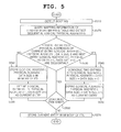
- FIG. 5 is a view illustrating a process flow when a main computing system is booted, according to an embodiment of the present invention.
- step S 520 is a step for querying the mapping information of a flash memory mapping table and for detecting sequential logical/physical addresses.
- the mapping information querying unit 210 executes a read operation on the system area of the flash memory, whereby the flash memory mapping table stored in the flash memory, which is the mapping information between logical addresses and physical addresses, is found.
- the detection unit 220 detects sequential logical addresses and sequential physical addresses corresponding to the sequential logical addresses, based on the mapping information of the flash memory mapping table found by the mapping information querying unit 210 .
- the mapping information of the flash memory mapping table includes a start logical address, a start physical address corresponding to the start logical address, and the size of sequential data. If the mapping information of the FTL is not condensed and stored in the mapping information storage management unit 140 , the mapping information of the flash memory mapping table includes one-to-one page mapping information between the logical addresses and the physical addresses.
- the mapping information management unit 230 stores more condensed mapping information, which includes a start logical address, a start physical address, and the size of sequential data.
- the mapping information management unit 230 is present on the memory (DRAM) of the flash translation layer, and in this case, the mapping information stored in the memory of the flash translation layer is FTL mapping information in which the mapping information stored in the FTL memory 130 is condensed more.
- step S 530 it is checked whether the logical addresses and the physical addresses of the current entry (logical address i, physical address i, data size i) and the next entry (logical address i+1, physical address i+1, data size i+1), detected at step S 520 , are sequential.
- step S 550 the information condensed at step S 540 , that is, “(logical page 0 , physical page 0 , 32 )”, is defined as a current entry.
- step S 530 is executed again to compare the current entry and the next entry.
- step S 570 is executed to store the current entry in the memory of the flash translation layer. Namely, at step S 570 , (logical page 0 , physical page 0 , 32 ) is stored in the memory of the flash translation layer.
- the above mentioned process enables more condensed mapping information to be stored in the memory (DRAM) of the flash translation layer by further condensing the mapping information stored in the flash memory when the logical addresses and physical addresses thereof are sequential, whereby system boot performance may be improved.
- the current entry (logical address i, physical address i, data size i), namely, (logical page 0 , physical page 0 , 16 ) is stored in the memory of the flash translation layer at step S 580 .
- step S 590 the next entry (logical address i+1, physical address i+1, data size i+1), namely, (logical page 16 , physical page 16 , 16 ) is defined as a current entry.
- step S 530 is executed again to compare the current entry and the next entry.
- step S 570 is executed to store the current entry in the memory of the flash translation layer. Namely, at step S 570 , (logical page 16 , physical page 16 , 16 ) is stored in the memory of the flash translation layer.
- the present invention has been derived from research conducted as part of projects for supporting general researchers by the Ministry of Education, Science and Technology and the National Research Foundation of Korea [Project Management Number: 1345176071; Project Name: Research for system software supporting next-generation flash memory system].
- the flash memory-based page-level address mapping method may be implemented in the form of program instructions that can be executed by a variety of computer means, and may be stored in a computer-readable storage medium.
- the computer-readable storage medium may include program instructions, a data file, and a data structure solely or in combination.
- the program instructions that are stored in the medium may be designed and constructed particularly for the present invention, or may be known and available to those skilled in the field of computer software.
- Examples of the computer-readable storage medium include magnetic media such as a hard disk, a floppy disk and a magnetic tape, optical media such as CD-ROM and a DVD, magneto-optical media such as a floptical disk, and hardware devices particularly configured to store and execute program instructions such as ROM, RAM, and flash memory.
- Examples of the program instructions include not only machine language code that is constructed by a compiler but also high-level language code that can be executed by a computer using an interpreter or the like.
- the above-described hardware components may be configured to act as one or more software modules that perform the operation of the present invention, and vice versa.
- the present invention relates to a method and system for a page-level address mapping based on flash memory and, more particularly, to a method and system for improving system boot performance by decreasing the number of read operations by reducing the sizes of mapping information and a page mapping table, using sequential logical addresses and a data size.
- a flash memory-based page-level address mapping method includes a step for receiving a read operation from the file system, a step for searching the FTL mapping table for a start logical address, which is identical to the logical address requested by the read operation or is the closest to and smaller than the logical address requested by the read operation, a step for calculating a physical address corresponding to the read operation, using the found start logical address and the logical address requested by the read operation, and the step for reading data stored at the calculated physical address of the flash memory.
Applications Claiming Priority (3)
| Application Number | Priority Date | Filing Date | Title |
|---|---|---|---|
| KR1020130031375A KR101453313B1 (ko) | 2013-03-25 | 2013-03-25 | 플래시 메모리 기반의 페이지 주소 사상 방법 및 시스템 |
| KR10-2013-0031375 | 2013-03-25 | ||
| PCT/KR2013/012429 WO2014157817A1 (fr) | 2013-03-25 | 2013-12-31 | Procédé de mappage d'adresse de page basée sur une mémoire flash et système correspondant |
Publications (2)
| Publication Number | Publication Date |
|---|---|
| US20160048448A1 US20160048448A1 (en) | 2016-02-18 |
| US9830260B2 true US9830260B2 (en) | 2017-11-28 |
Family
ID=51624741
Family Applications (1)
| Application Number | Title | Priority Date | Filing Date |
|---|---|---|---|
| US14/779,954 Active US9830260B2 (en) | 2013-03-25 | 2013-12-31 | Method for mapping page address based on flash memory and system therefor |
Country Status (3)
| Country | Link |
|---|---|
| US (1) | US9830260B2 (fr) |
| KR (1) | KR101453313B1 (fr) |
| WO (1) | WO2014157817A1 (fr) |
Cited By (1)
| Publication number | Priority date | Publication date | Assignee | Title |
|---|---|---|---|---|
| US20170039141A1 (en) * | 2015-08-04 | 2017-02-09 | Phison Electronics Corp. | Mapping table updating method, memory storage device and memory control circuit unit |
Families Citing this family (24)
| Publication number | Priority date | Publication date | Assignee | Title |
|---|---|---|---|---|
| KR20170012629A (ko) | 2015-07-21 | 2017-02-03 | 에스케이하이닉스 주식회사 | 메모리 시스템 및 메모리 시스템의 동작 방법 |
| DE102015225553A1 (de) * | 2015-12-17 | 2017-06-22 | Robert Bosch Gmbh | Verfahren und Vorrichtung zur Verwaltung eines nichtflüchtigen Speichers für ein Steuergerät |
| US10248333B1 (en) | 2017-02-07 | 2019-04-02 | Crossbar, Inc. | Write distribution techniques for two-terminal memory wear leveling |
| US10409714B1 (en) * | 2017-02-09 | 2019-09-10 | Crossbar, Inc. | Logical to physical translation for two-terminal memory |
| CN107015764B (zh) * | 2017-03-17 | 2020-03-27 | 深圳市江波龙电子股份有限公司 | Nand flash的数据处理方法、装置和一种Nand flash |
| WO2018232089A1 (fr) * | 2017-06-14 | 2018-12-20 | Burlywood, LLC | Gestion de table de localisation de données fondée sur une étendue |
| CN107391393A (zh) * | 2017-07-28 | 2017-11-24 | 郑州云海信息技术有限公司 | 一种ftl映射表的统计方法及装置 |
| CN107291405B (zh) * | 2017-08-17 | 2020-05-26 | 北京中电华大电子设计有限责任公司 | 一种NorFlash的数据管理方法与装置 |
| KR20190083051A (ko) | 2018-01-03 | 2019-07-11 | 에스케이하이닉스 주식회사 | 컨트롤러 및 그것의 동작방법 |
| KR20190123502A (ko) | 2018-04-24 | 2019-11-01 | 에스케이하이닉스 주식회사 | 메모리 시스템 및 메모리 시스템의 동작방법 |
| CN109491927B (zh) * | 2018-11-06 | 2023-02-03 | 镕铭微电子(济南)有限公司 | 数据存储、读取方法、装置及电子设备 |
| US11093170B2 (en) * | 2019-04-02 | 2021-08-17 | EMC IP Holding Company LLC | Dataset splitting based on workload footprint analysis |
| US11068204B2 (en) * | 2019-05-22 | 2021-07-20 | Macronix International Co., Ltd. | Memory device with multiple physical spaces, multiple non-volatile memory arrays, multiple main data, multiple metadata of multiple types of commands, and access method thereof |
| CN110309081B (zh) * | 2019-06-03 | 2022-11-01 | 华侨大学 | 基于压缩存储和地址映射表项的ftl读写数据页的方法 |
| US11282567B2 (en) * | 2019-08-20 | 2022-03-22 | Micron Technology, Inc. | Sequential SLC read optimization |
| US11281578B2 (en) | 2019-08-20 | 2022-03-22 | Micron Technology, Inc. | Garbage collection in a memory sub-system during a low battery state |
| US11726869B2 (en) | 2019-08-20 | 2023-08-15 | Micron Technology, Inc. | Performing error control operation on memory component for garbage collection |
| US11281392B2 (en) | 2019-08-28 | 2022-03-22 | Micron Technology, Inc. | Garbage collection in a memory component using an adjusted parameter |
| CN111858395B (zh) * | 2020-06-30 | 2024-03-19 | 维沃移动通信有限公司 | 数据管理方法及装置 |
| CN113076267B (zh) * | 2021-04-29 | 2023-05-26 | 华侨大学 | 一种基于热点汇集的地址转换方法和数据存储装置 |
| US11940926B2 (en) * | 2022-05-13 | 2024-03-26 | Micron Technology, Inc. | Creating high density logical to physical mapping |
| CN114968120B (zh) * | 2022-06-01 | 2023-06-06 | 上海佳勒电子有限公司 | 一种提高单片机flash存储次数的数据处理方法及系统 |
| CN116010298B (zh) * | 2023-03-24 | 2023-09-22 | 温州市特种设备检测科学研究院(温州市特种设备应急处置中心) | Nand型闪存地址映射的方法、装置、电子设备及存储介质 |
| CN117370222A (zh) * | 2023-12-08 | 2024-01-09 | 成都佰维存储科技有限公司 | 存储映射方法、装置、计算机可读存储介质及电子设备 |
Citations (18)
| Publication number | Priority date | Publication date | Assignee | Title |
|---|---|---|---|---|
| KR20030095820A (ko) | 2002-06-14 | 2003-12-24 | 주식회사 포인칩스 | 메모리 억세스 제어장치 및 방법 |
| US20050144368A1 (en) * | 2003-12-30 | 2005-06-30 | Samsung Electronics Co., Ltd. | Address mapping method and mapping information managing method for flash memory, and flash memory using the same |
| US20100125694A1 (en) * | 2008-11-18 | 2010-05-20 | Gyu Sang Choi | Memory device and management method of memory device |
| KR100965051B1 (ko) | 2008-10-01 | 2010-06-21 | 서울시립대학교 산학협력단 | 플래시 메모리 장치를 위한 가변 공간 페이지 사상 방법 및그 장치 |
| US20100257309A1 (en) * | 2009-04-06 | 2010-10-07 | Boris Barsky | Device and method for managing a flash memory |
| US20100332732A1 (en) | 2009-06-29 | 2010-12-30 | Mediatek Inc. | Memory systems and mapping methods thereof |
| US8019925B1 (en) * | 2004-05-06 | 2011-09-13 | Seagate Technology Llc | Methods and structure for dynamically mapped mass storage device |
| KR20120037218A (ko) | 2010-10-11 | 2012-04-19 | 성균관대학교산학협력단 | Ssd 장치의 매핑 테이블 관리 방법 |
| US20120110239A1 (en) * | 2010-10-27 | 2012-05-03 | Seagate Technology Llc | Causing Related Data to be Written Together to Non-Volatile, Solid State Memory |
| KR20120074707A (ko) | 2010-12-28 | 2012-07-06 | 한양대학교 산학협력단 | 플래시 메모리를 사용하는 저장장치 및 주소 사상과 데이터 페이지 할당 방법 |
| KR101191650B1 (ko) | 2010-10-04 | 2012-10-17 | 한국과학기술원 | 낸드 플래시 메모리에서 데이터의 주소를 사상시키는 장치 및 방법 |
| US20120278560A1 (en) * | 2009-10-04 | 2012-11-01 | Infinidat Ltd. | Pre-fetching in a storage system that maintains a mapping tree |
| KR101319589B1 (ko) | 2011-08-12 | 2013-10-16 | 아주대학교산학협력단 | 솔리드 스테이트 드라이브의 쓰기 데이터 분별 방법 및 그 컨트롤러 |
| US20140164687A1 (en) | 2011-08-12 | 2014-06-12 | Ajou University Industry-Academic Cooperation Foundation | Memory controller and data management method thereof |
| US20140164730A1 (en) * | 2012-12-10 | 2014-06-12 | Infinidat Ltd. | System and methods for managing storage space allocation |
| US20150081961A1 (en) | 2012-05-23 | 2015-03-19 | Ajou University Industry-Academic | Method and device for identifying information for chip-level parallel flash memory |
| US20150205525A1 (en) * | 2014-01-18 | 2015-07-23 | International Business Machines Corporation | Fine-grained data reorganization in tiered storage architectures |
| US9697116B2 (en) * | 2013-08-08 | 2017-07-04 | Samsung Electronics Co., Ltd. | Storage system and writing method thereof |
-
2013
- 2013-03-25 KR KR1020130031375A patent/KR101453313B1/ko active IP Right Grant
- 2013-12-31 US US14/779,954 patent/US9830260B2/en active Active
- 2013-12-31 WO PCT/KR2013/012429 patent/WO2014157817A1/fr active Application Filing
Patent Citations (18)
| Publication number | Priority date | Publication date | Assignee | Title |
|---|---|---|---|---|
| KR20030095820A (ko) | 2002-06-14 | 2003-12-24 | 주식회사 포인칩스 | 메모리 억세스 제어장치 및 방법 |
| US20050144368A1 (en) * | 2003-12-30 | 2005-06-30 | Samsung Electronics Co., Ltd. | Address mapping method and mapping information managing method for flash memory, and flash memory using the same |
| US8019925B1 (en) * | 2004-05-06 | 2011-09-13 | Seagate Technology Llc | Methods and structure for dynamically mapped mass storage device |
| KR100965051B1 (ko) | 2008-10-01 | 2010-06-21 | 서울시립대학교 산학협력단 | 플래시 메모리 장치를 위한 가변 공간 페이지 사상 방법 및그 장치 |
| US20100125694A1 (en) * | 2008-11-18 | 2010-05-20 | Gyu Sang Choi | Memory device and management method of memory device |
| US20100257309A1 (en) * | 2009-04-06 | 2010-10-07 | Boris Barsky | Device and method for managing a flash memory |
| US20100332732A1 (en) | 2009-06-29 | 2010-12-30 | Mediatek Inc. | Memory systems and mapping methods thereof |
| US20120278560A1 (en) * | 2009-10-04 | 2012-11-01 | Infinidat Ltd. | Pre-fetching in a storage system that maintains a mapping tree |
| KR101191650B1 (ko) | 2010-10-04 | 2012-10-17 | 한국과학기술원 | 낸드 플래시 메모리에서 데이터의 주소를 사상시키는 장치 및 방법 |
| KR20120037218A (ko) | 2010-10-11 | 2012-04-19 | 성균관대학교산학협력단 | Ssd 장치의 매핑 테이블 관리 방법 |
| US20120110239A1 (en) * | 2010-10-27 | 2012-05-03 | Seagate Technology Llc | Causing Related Data to be Written Together to Non-Volatile, Solid State Memory |
| KR20120074707A (ko) | 2010-12-28 | 2012-07-06 | 한양대학교 산학협력단 | 플래시 메모리를 사용하는 저장장치 및 주소 사상과 데이터 페이지 할당 방법 |
| KR101319589B1 (ko) | 2011-08-12 | 2013-10-16 | 아주대학교산학협력단 | 솔리드 스테이트 드라이브의 쓰기 데이터 분별 방법 및 그 컨트롤러 |
| US20140164687A1 (en) | 2011-08-12 | 2014-06-12 | Ajou University Industry-Academic Cooperation Foundation | Memory controller and data management method thereof |
| US20150081961A1 (en) | 2012-05-23 | 2015-03-19 | Ajou University Industry-Academic | Method and device for identifying information for chip-level parallel flash memory |
| US20140164730A1 (en) * | 2012-12-10 | 2014-06-12 | Infinidat Ltd. | System and methods for managing storage space allocation |
| US9697116B2 (en) * | 2013-08-08 | 2017-07-04 | Samsung Electronics Co., Ltd. | Storage system and writing method thereof |
| US20150205525A1 (en) * | 2014-01-18 | 2015-07-23 | International Business Machines Corporation | Fine-grained data reorganization in tiered storage architectures |
Non-Patent Citations (1)
| Title |
|---|
| International Search Report dated Mar. 18, 2014, issued to International Application No. PCT/KR2013/012429. |
Cited By (1)
| Publication number | Priority date | Publication date | Assignee | Title |
|---|---|---|---|---|
| US20170039141A1 (en) * | 2015-08-04 | 2017-02-09 | Phison Electronics Corp. | Mapping table updating method, memory storage device and memory control circuit unit |
Also Published As
| Publication number | Publication date |
|---|---|
| US20160048448A1 (en) | 2016-02-18 |
| KR20140116617A (ko) | 2014-10-06 |
| KR101453313B1 (ko) | 2014-10-22 |
| WO2014157817A1 (fr) | 2014-10-02 |
Similar Documents
| Publication | Publication Date | Title |
|---|---|---|
| US9830260B2 (en) | Method for mapping page address based on flash memory and system therefor | |
| CN108804350B (zh) | 一种内存访问方法及计算机系统 | |
| US7930515B2 (en) | Virtual memory management | |
| JP6696987B2 (ja) | 仮想アドレスを使用してアクセスされるキャッシュ | |
| TWI515563B (zh) | 用於階層式記憶體系統之記憶體管理 | |
| US9081661B2 (en) | Memory management device and method for managing access to a nonvolatile semiconductor memory | |
| US7953953B2 (en) | Method and apparatus for reducing page replacement time in system using demand paging technique | |
| US20100312955A1 (en) | Memory system and method of managing the same | |
| JP5709814B2 (ja) | 不揮発性メモリを有するシステムのための高速ツリー平坦化 | |
| KR20120058352A (ko) | 하이브리드 메모리 시스템, 및 그 관리 방법 | |
| KR20130032603A (ko) | 다양한 블록 크기를 지원하는 주소 사상을 사용하여 플래시 메모리 내에 데이터를 저장하는 방법 및 장치 | |
| KR20100081880A (ko) | 비휘발성 메모리와, 이의 페이지 동적할당장치 및 페이지 매핑장치와, 이의 페이지 동적할당방법 및 페이지 매핑방법 | |
| JP2017208096A (ja) | データの回収方法及び格納方法並びに重複除去モジュール | |
| US7870122B2 (en) | Self-tuning index for flash-based databases | |
| US20120030405A1 (en) | Information processing device and information processing method | |
| US20240143219A1 (en) | Software-hardware combination method for internal mapping address query of zoned namespace | |
| US20170039142A1 (en) | Persistent Memory Manager | |
| EP3163451B1 (fr) | Procédé et dispositif de gestion de mémoire et contrôleur de mémoire | |
| JP2007220107A (ja) | 不揮発性メモリのマッピング情報管理装置及び方法 | |
| CN114546898A (zh) | 一种tlb管理方法、装置、设备及存储介质 | |
| US9329994B2 (en) | Memory system | |
| JP2016085677A (ja) | メモリ管理方法、メモリ管理プログラム及び情報処理装置 | |
| US9336413B2 (en) | Method and system for fast permission changes for virtual addresses | |
| US20220358051A1 (en) | Non-volatile storage controller with partial logical-to-physical (l2p) address translation table | |
| WO2015161804A1 (fr) | Procédé et dispositif de partitionnement de mémoire cache |
Legal Events
| Date | Code | Title | Description |
|---|---|---|---|
| AS | Assignment |
Owner name: AJOU UNIVERSITY INDUSTRY-ACADEMIC COOPERATION FOUN Free format text: ASSIGNMENT OF ASSIGNORS INTEREST;ASSIGNORS:KWON, SE JIN;CHUNG, TAE SUN;BAN, JAE KWANG;AND OTHERS;REEL/FRAME:036653/0606 Effective date: 20150921 |
|
| STCF | Information on status: patent grant |
Free format text: PATENTED CASE |
|
| MAFP | Maintenance fee payment |
Free format text: PAYMENT OF MAINTENANCE FEE, 4TH YR, SMALL ENTITY (ORIGINAL EVENT CODE: M2551); ENTITY STATUS OF PATENT OWNER: SMALL ENTITY Year of fee payment: 4 |