US9818736B1 - Method for producing semiconductor package - Google Patents
Method for producing semiconductor package Download PDFInfo
- Publication number
- US9818736B1 US9818736B1 US15/449,074 US201715449074A US9818736B1 US 9818736 B1 US9818736 B1 US 9818736B1 US 201715449074 A US201715449074 A US 201715449074A US 9818736 B1 US9818736 B1 US 9818736B1
- Authority
- US
- United States
- Prior art keywords
- microbump
- semiconductor chips
- smooth surface
- semiconductor
- microbumps
- Prior art date
- Legal status (The legal status is an assumption and is not a legal conclusion. Google has not performed a legal analysis and makes no representation as to the accuracy of the status listed.)
- Active
Links
Images


Classifications
-
- H—ELECTRICITY
- H01—ELECTRIC ELEMENTS
- H01L—SEMICONDUCTOR DEVICES NOT COVERED BY CLASS H10
- H01L24/00—Arrangements for connecting or disconnecting semiconductor or solid-state bodies; Methods or apparatus related thereto
- H01L24/80—Methods for connecting semiconductor or other solid state bodies using means for bonding being attached to, or being formed on, the surface to be connected
- H01L24/81—Methods for connecting semiconductor or other solid state bodies using means for bonding being attached to, or being formed on, the surface to be connected using a bump connector
-
- H—ELECTRICITY
- H01—ELECTRIC ELEMENTS
- H01L—SEMICONDUCTOR DEVICES NOT COVERED BY CLASS H10
- H01L25/00—Assemblies consisting of a plurality of individual semiconductor or other solid state devices ; Multistep manufacturing processes thereof
- H01L25/50—Multistep manufacturing processes of assemblies consisting of devices, each device being of a type provided for in group H01L27/00 or H01L29/00
-
- H—ELECTRICITY
- H01—ELECTRIC ELEMENTS
- H01L—SEMICONDUCTOR DEVICES NOT COVERED BY CLASS H10
- H01L21/00—Processes or apparatus adapted for the manufacture or treatment of semiconductor or solid state devices or of parts thereof
- H01L21/02—Manufacture or treatment of semiconductor devices or of parts thereof
- H01L21/04—Manufacture or treatment of semiconductor devices or of parts thereof the devices having at least one potential-jump barrier or surface barrier, e.g. PN junction, depletion layer or carrier concentration layer
- H01L21/50—Assembly of semiconductor devices using processes or apparatus not provided for in a single one of the subgroups H01L21/06 - H01L21/326, e.g. sealing of a cap to a base of a container
- H01L21/56—Encapsulations, e.g. encapsulation layers, coatings
- H01L21/563—Encapsulation of active face of flip-chip device, e.g. underfilling or underencapsulation of flip-chip, encapsulation preform on chip or mounting substrate
-
- H—ELECTRICITY
- H01—ELECTRIC ELEMENTS
- H01L—SEMICONDUCTOR DEVICES NOT COVERED BY CLASS H10
- H01L23/00—Details of semiconductor or other solid state devices
- H01L23/48—Arrangements for conducting electric current to or from the solid state body in operation, e.g. leads, terminal arrangements ; Selection of materials therefor
- H01L23/488—Arrangements for conducting electric current to or from the solid state body in operation, e.g. leads, terminal arrangements ; Selection of materials therefor consisting of soldered or bonded constructions
- H01L23/498—Leads, i.e. metallisations or lead-frames on insulating substrates, e.g. chip carriers
- H01L23/49811—Additional leads joined to the metallisation on the insulating substrate, e.g. pins, bumps, wires, flat leads
-
- H—ELECTRICITY
- H01—ELECTRIC ELEMENTS
- H01L—SEMICONDUCTOR DEVICES NOT COVERED BY CLASS H10
- H01L24/00—Arrangements for connecting or disconnecting semiconductor or solid-state bodies; Methods or apparatus related thereto
- H01L24/01—Means for bonding being attached to, or being formed on, the surface to be connected, e.g. chip-to-package, die-attach, "first-level" interconnects; Manufacturing methods related thereto
- H01L24/10—Bump connectors ; Manufacturing methods related thereto
- H01L24/11—Manufacturing methods
-
- H—ELECTRICITY
- H01—ELECTRIC ELEMENTS
- H01L—SEMICONDUCTOR DEVICES NOT COVERED BY CLASS H10
- H01L24/00—Arrangements for connecting or disconnecting semiconductor or solid-state bodies; Methods or apparatus related thereto
- H01L24/01—Means for bonding being attached to, or being formed on, the surface to be connected, e.g. chip-to-package, die-attach, "first-level" interconnects; Manufacturing methods related thereto
- H01L24/10—Bump connectors ; Manufacturing methods related thereto
- H01L24/12—Structure, shape, material or disposition of the bump connectors prior to the connecting process
- H01L24/14—Structure, shape, material or disposition of the bump connectors prior to the connecting process of a plurality of bump connectors
-
- H—ELECTRICITY
- H01—ELECTRIC ELEMENTS
- H01L—SEMICONDUCTOR DEVICES NOT COVERED BY CLASS H10
- H01L24/00—Arrangements for connecting or disconnecting semiconductor or solid-state bodies; Methods or apparatus related thereto
- H01L24/01—Means for bonding being attached to, or being formed on, the surface to be connected, e.g. chip-to-package, die-attach, "first-level" interconnects; Manufacturing methods related thereto
- H01L24/10—Bump connectors ; Manufacturing methods related thereto
- H01L24/15—Structure, shape, material or disposition of the bump connectors after the connecting process
- H01L24/16—Structure, shape, material or disposition of the bump connectors after the connecting process of an individual bump connector
-
- H—ELECTRICITY
- H01—ELECTRIC ELEMENTS
- H01L—SEMICONDUCTOR DEVICES NOT COVERED BY CLASS H10
- H01L25/00—Assemblies consisting of a plurality of individual semiconductor or other solid state devices ; Multistep manufacturing processes thereof
- H01L25/03—Assemblies consisting of a plurality of individual semiconductor or other solid state devices ; Multistep manufacturing processes thereof all the devices being of a type provided for in the same subgroup of groups H01L27/00 - H01L33/00, or in a single subclass of H10K, H10N, e.g. assemblies of rectifier diodes
- H01L25/04—Assemblies consisting of a plurality of individual semiconductor or other solid state devices ; Multistep manufacturing processes thereof all the devices being of a type provided for in the same subgroup of groups H01L27/00 - H01L33/00, or in a single subclass of H10K, H10N, e.g. assemblies of rectifier diodes the devices not having separate containers
- H01L25/065—Assemblies consisting of a plurality of individual semiconductor or other solid state devices ; Multistep manufacturing processes thereof all the devices being of a type provided for in the same subgroup of groups H01L27/00 - H01L33/00, or in a single subclass of H10K, H10N, e.g. assemblies of rectifier diodes the devices not having separate containers the devices being of a type provided for in group H01L27/00
- H01L25/0657—Stacked arrangements of devices
-
- H—ELECTRICITY
- H01—ELECTRIC ELEMENTS
- H01L—SEMICONDUCTOR DEVICES NOT COVERED BY CLASS H10
- H01L2224/00—Indexing scheme for arrangements for connecting or disconnecting semiconductor or solid-state bodies and methods related thereto as covered by H01L24/00
- H01L2224/01—Means for bonding being attached to, or being formed on, the surface to be connected, e.g. chip-to-package, die-attach, "first-level" interconnects; Manufacturing methods related thereto
- H01L2224/02—Bonding areas; Manufacturing methods related thereto
- H01L2224/04—Structure, shape, material or disposition of the bonding areas prior to the connecting process
- H01L2224/0401—Bonding areas specifically adapted for bump connectors, e.g. under bump metallisation [UBM]
-
- H—ELECTRICITY
- H01—ELECTRIC ELEMENTS
- H01L—SEMICONDUCTOR DEVICES NOT COVERED BY CLASS H10
- H01L2224/00—Indexing scheme for arrangements for connecting or disconnecting semiconductor or solid-state bodies and methods related thereto as covered by H01L24/00
- H01L2224/01—Means for bonding being attached to, or being formed on, the surface to be connected, e.g. chip-to-package, die-attach, "first-level" interconnects; Manufacturing methods related thereto
- H01L2224/02—Bonding areas; Manufacturing methods related thereto
- H01L2224/04—Structure, shape, material or disposition of the bonding areas prior to the connecting process
- H01L2224/05—Structure, shape, material or disposition of the bonding areas prior to the connecting process of an individual bonding area
- H01L2224/05001—Internal layers
- H01L2224/0502—Disposition
- H01L2224/05025—Disposition the internal layer being disposed on a via connection of the semiconductor or solid-state body
-
- H—ELECTRICITY
- H01—ELECTRIC ELEMENTS
- H01L—SEMICONDUCTOR DEVICES NOT COVERED BY CLASS H10
- H01L2224/00—Indexing scheme for arrangements for connecting or disconnecting semiconductor or solid-state bodies and methods related thereto as covered by H01L24/00
- H01L2224/01—Means for bonding being attached to, or being formed on, the surface to be connected, e.g. chip-to-package, die-attach, "first-level" interconnects; Manufacturing methods related thereto
- H01L2224/02—Bonding areas; Manufacturing methods related thereto
- H01L2224/04—Structure, shape, material or disposition of the bonding areas prior to the connecting process
- H01L2224/05—Structure, shape, material or disposition of the bonding areas prior to the connecting process of an individual bonding area
- H01L2224/05001—Internal layers
- H01L2224/05099—Material
- H01L2224/051—Material with a principal constituent of the material being a metal or a metalloid, e.g. boron [B], silicon [Si], germanium [Ge], arsenic [As], antimony [Sb], tellurium [Te] and polonium [Po], and alloys thereof
- H01L2224/05138—Material with a principal constituent of the material being a metal or a metalloid, e.g. boron [B], silicon [Si], germanium [Ge], arsenic [As], antimony [Sb], tellurium [Te] and polonium [Po], and alloys thereof the principal constituent melting at a temperature of greater than or equal to 950°C and less than 1550°C
- H01L2224/05147—Copper [Cu] as principal constituent
-
- H—ELECTRICITY
- H01—ELECTRIC ELEMENTS
- H01L—SEMICONDUCTOR DEVICES NOT COVERED BY CLASS H10
- H01L2224/00—Indexing scheme for arrangements for connecting or disconnecting semiconductor or solid-state bodies and methods related thereto as covered by H01L24/00
- H01L2224/01—Means for bonding being attached to, or being formed on, the surface to be connected, e.g. chip-to-package, die-attach, "first-level" interconnects; Manufacturing methods related thereto
- H01L2224/02—Bonding areas; Manufacturing methods related thereto
- H01L2224/04—Structure, shape, material or disposition of the bonding areas prior to the connecting process
- H01L2224/05—Structure, shape, material or disposition of the bonding areas prior to the connecting process of an individual bonding area
- H01L2224/0554—External layer
- H01L2224/05599—Material
- H01L2224/056—Material with a principal constituent of the material being a metal or a metalloid, e.g. boron [B], silicon [Si], germanium [Ge], arsenic [As], antimony [Sb], tellurium [Te] and polonium [Po], and alloys thereof
- H01L2224/05638—Material with a principal constituent of the material being a metal or a metalloid, e.g. boron [B], silicon [Si], germanium [Ge], arsenic [As], antimony [Sb], tellurium [Te] and polonium [Po], and alloys thereof the principal constituent melting at a temperature of greater than or equal to 950°C and less than 1550°C
- H01L2224/05655—Nickel [Ni] as principal constituent
-
- H—ELECTRICITY
- H01—ELECTRIC ELEMENTS
- H01L—SEMICONDUCTOR DEVICES NOT COVERED BY CLASS H10
- H01L2224/00—Indexing scheme for arrangements for connecting or disconnecting semiconductor or solid-state bodies and methods related thereto as covered by H01L24/00
- H01L2224/01—Means for bonding being attached to, or being formed on, the surface to be connected, e.g. chip-to-package, die-attach, "first-level" interconnects; Manufacturing methods related thereto
- H01L2224/02—Bonding areas; Manufacturing methods related thereto
- H01L2224/04—Structure, shape, material or disposition of the bonding areas prior to the connecting process
- H01L2224/05—Structure, shape, material or disposition of the bonding areas prior to the connecting process of an individual bonding area
- H01L2224/0554—External layer
- H01L2224/05599—Material
- H01L2224/05686—Material with a principal constituent of the material being a non metallic, non metalloid inorganic material
-
- H—ELECTRICITY
- H01—ELECTRIC ELEMENTS
- H01L—SEMICONDUCTOR DEVICES NOT COVERED BY CLASS H10
- H01L2224/00—Indexing scheme for arrangements for connecting or disconnecting semiconductor or solid-state bodies and methods related thereto as covered by H01L24/00
- H01L2224/01—Means for bonding being attached to, or being formed on, the surface to be connected, e.g. chip-to-package, die-attach, "first-level" interconnects; Manufacturing methods related thereto
- H01L2224/02—Bonding areas; Manufacturing methods related thereto
- H01L2224/04—Structure, shape, material or disposition of the bonding areas prior to the connecting process
- H01L2224/06—Structure, shape, material or disposition of the bonding areas prior to the connecting process of a plurality of bonding areas
- H01L2224/061—Disposition
- H01L2224/0618—Disposition being disposed on at least two different sides of the body, e.g. dual array
- H01L2224/06181—On opposite sides of the body
-
- H—ELECTRICITY
- H01—ELECTRIC ELEMENTS
- H01L—SEMICONDUCTOR DEVICES NOT COVERED BY CLASS H10
- H01L2224/00—Indexing scheme for arrangements for connecting or disconnecting semiconductor or solid-state bodies and methods related thereto as covered by H01L24/00
- H01L2224/01—Means for bonding being attached to, or being formed on, the surface to be connected, e.g. chip-to-package, die-attach, "first-level" interconnects; Manufacturing methods related thereto
- H01L2224/10—Bump connectors; Manufacturing methods related thereto
- H01L2224/11—Manufacturing methods
- H01L2224/11001—Involving a temporary auxiliary member not forming part of the manufacturing apparatus, e.g. removable or sacrificial coating, film or substrate
- H01L2224/11005—Involving a temporary auxiliary member not forming part of the manufacturing apparatus, e.g. removable or sacrificial coating, film or substrate for aligning the bump connector, e.g. marks, spacers
-
- H—ELECTRICITY
- H01—ELECTRIC ELEMENTS
- H01L—SEMICONDUCTOR DEVICES NOT COVERED BY CLASS H10
- H01L2224/00—Indexing scheme for arrangements for connecting or disconnecting semiconductor or solid-state bodies and methods related thereto as covered by H01L24/00
- H01L2224/01—Means for bonding being attached to, or being formed on, the surface to be connected, e.g. chip-to-package, die-attach, "first-level" interconnects; Manufacturing methods related thereto
- H01L2224/10—Bump connectors; Manufacturing methods related thereto
- H01L2224/11—Manufacturing methods
- H01L2224/113—Manufacturing methods by local deposition of the material of the bump connector
- H01L2224/1133—Manufacturing methods by local deposition of the material of the bump connector in solid form
- H01L2224/11332—Manufacturing methods by local deposition of the material of the bump connector in solid form using a powder
-
- H—ELECTRICITY
- H01—ELECTRIC ELEMENTS
- H01L—SEMICONDUCTOR DEVICES NOT COVERED BY CLASS H10
- H01L2224/00—Indexing scheme for arrangements for connecting or disconnecting semiconductor or solid-state bodies and methods related thereto as covered by H01L24/00
- H01L2224/01—Means for bonding being attached to, or being formed on, the surface to be connected, e.g. chip-to-package, die-attach, "first-level" interconnects; Manufacturing methods related thereto
- H01L2224/10—Bump connectors; Manufacturing methods related thereto
- H01L2224/11—Manufacturing methods
- H01L2224/114—Manufacturing methods by blanket deposition of the material of the bump connector
- H01L2224/1146—Plating
-
- H—ELECTRICITY
- H01—ELECTRIC ELEMENTS
- H01L—SEMICONDUCTOR DEVICES NOT COVERED BY CLASS H10
- H01L2224/00—Indexing scheme for arrangements for connecting or disconnecting semiconductor or solid-state bodies and methods related thereto as covered by H01L24/00
- H01L2224/01—Means for bonding being attached to, or being formed on, the surface to be connected, e.g. chip-to-package, die-attach, "first-level" interconnects; Manufacturing methods related thereto
- H01L2224/10—Bump connectors; Manufacturing methods related thereto
- H01L2224/11—Manufacturing methods
- H01L2224/118—Post-treatment of the bump connector
- H01L2224/1183—Reworking, e.g. shaping
- H01L2224/1184—Reworking, e.g. shaping involving a mechanical process, e.g. planarising the bump connector
-
- H—ELECTRICITY
- H01—ELECTRIC ELEMENTS
- H01L—SEMICONDUCTOR DEVICES NOT COVERED BY CLASS H10
- H01L2224/00—Indexing scheme for arrangements for connecting or disconnecting semiconductor or solid-state bodies and methods related thereto as covered by H01L24/00
- H01L2224/01—Means for bonding being attached to, or being formed on, the surface to be connected, e.g. chip-to-package, die-attach, "first-level" interconnects; Manufacturing methods related thereto
- H01L2224/10—Bump connectors; Manufacturing methods related thereto
- H01L2224/11—Manufacturing methods
- H01L2224/118—Post-treatment of the bump connector
- H01L2224/11848—Thermal treatments, e.g. annealing, controlled cooling
- H01L2224/11849—Reflowing
-
- H—ELECTRICITY
- H01—ELECTRIC ELEMENTS
- H01L—SEMICONDUCTOR DEVICES NOT COVERED BY CLASS H10
- H01L2224/00—Indexing scheme for arrangements for connecting or disconnecting semiconductor or solid-state bodies and methods related thereto as covered by H01L24/00
- H01L2224/01—Means for bonding being attached to, or being formed on, the surface to be connected, e.g. chip-to-package, die-attach, "first-level" interconnects; Manufacturing methods related thereto
- H01L2224/10—Bump connectors; Manufacturing methods related thereto
- H01L2224/12—Structure, shape, material or disposition of the bump connectors prior to the connecting process
- H01L2224/13—Structure, shape, material or disposition of the bump connectors prior to the connecting process of an individual bump connector
- H01L2224/13001—Core members of the bump connector
- H01L2224/1302—Disposition
- H01L2224/13022—Disposition the bump connector being at least partially embedded in the surface
-
- H—ELECTRICITY
- H01—ELECTRIC ELEMENTS
- H01L—SEMICONDUCTOR DEVICES NOT COVERED BY CLASS H10
- H01L2224/00—Indexing scheme for arrangements for connecting or disconnecting semiconductor or solid-state bodies and methods related thereto as covered by H01L24/00
- H01L2224/01—Means for bonding being attached to, or being formed on, the surface to be connected, e.g. chip-to-package, die-attach, "first-level" interconnects; Manufacturing methods related thereto
- H01L2224/10—Bump connectors; Manufacturing methods related thereto
- H01L2224/12—Structure, shape, material or disposition of the bump connectors prior to the connecting process
- H01L2224/13—Structure, shape, material or disposition of the bump connectors prior to the connecting process of an individual bump connector
- H01L2224/13001—Core members of the bump connector
- H01L2224/13075—Plural core members
- H01L2224/1308—Plural core members being stacked
- H01L2224/13083—Three-layer arrangements
-
- H—ELECTRICITY
- H01—ELECTRIC ELEMENTS
- H01L—SEMICONDUCTOR DEVICES NOT COVERED BY CLASS H10
- H01L2224/00—Indexing scheme for arrangements for connecting or disconnecting semiconductor or solid-state bodies and methods related thereto as covered by H01L24/00
- H01L2224/01—Means for bonding being attached to, or being formed on, the surface to be connected, e.g. chip-to-package, die-attach, "first-level" interconnects; Manufacturing methods related thereto
- H01L2224/10—Bump connectors; Manufacturing methods related thereto
- H01L2224/12—Structure, shape, material or disposition of the bump connectors prior to the connecting process
- H01L2224/13—Structure, shape, material or disposition of the bump connectors prior to the connecting process of an individual bump connector
- H01L2224/13001—Core members of the bump connector
- H01L2224/13099—Material
- H01L2224/131—Material with a principal constituent of the material being a metal or a metalloid, e.g. boron [B], silicon [Si], germanium [Ge], arsenic [As], antimony [Sb], tellurium [Te] and polonium [Po], and alloys thereof
- H01L2224/13101—Material with a principal constituent of the material being a metal or a metalloid, e.g. boron [B], silicon [Si], germanium [Ge], arsenic [As], antimony [Sb], tellurium [Te] and polonium [Po], and alloys thereof the principal constituent melting at a temperature of less than 400°C
- H01L2224/13109—Indium [In] as principal constituent
-
- H—ELECTRICITY
- H01—ELECTRIC ELEMENTS
- H01L—SEMICONDUCTOR DEVICES NOT COVERED BY CLASS H10
- H01L2224/00—Indexing scheme for arrangements for connecting or disconnecting semiconductor or solid-state bodies and methods related thereto as covered by H01L24/00
- H01L2224/01—Means for bonding being attached to, or being formed on, the surface to be connected, e.g. chip-to-package, die-attach, "first-level" interconnects; Manufacturing methods related thereto
- H01L2224/10—Bump connectors; Manufacturing methods related thereto
- H01L2224/12—Structure, shape, material or disposition of the bump connectors prior to the connecting process
- H01L2224/13—Structure, shape, material or disposition of the bump connectors prior to the connecting process of an individual bump connector
- H01L2224/13001—Core members of the bump connector
- H01L2224/13099—Material
- H01L2224/131—Material with a principal constituent of the material being a metal or a metalloid, e.g. boron [B], silicon [Si], germanium [Ge], arsenic [As], antimony [Sb], tellurium [Te] and polonium [Po], and alloys thereof
- H01L2224/13101—Material with a principal constituent of the material being a metal or a metalloid, e.g. boron [B], silicon [Si], germanium [Ge], arsenic [As], antimony [Sb], tellurium [Te] and polonium [Po], and alloys thereof the principal constituent melting at a temperature of less than 400°C
- H01L2224/13111—Tin [Sn] as principal constituent
-
- H—ELECTRICITY
- H01—ELECTRIC ELEMENTS
- H01L—SEMICONDUCTOR DEVICES NOT COVERED BY CLASS H10
- H01L2224/00—Indexing scheme for arrangements for connecting or disconnecting semiconductor or solid-state bodies and methods related thereto as covered by H01L24/00
- H01L2224/01—Means for bonding being attached to, or being formed on, the surface to be connected, e.g. chip-to-package, die-attach, "first-level" interconnects; Manufacturing methods related thereto
- H01L2224/10—Bump connectors; Manufacturing methods related thereto
- H01L2224/12—Structure, shape, material or disposition of the bump connectors prior to the connecting process
- H01L2224/13—Structure, shape, material or disposition of the bump connectors prior to the connecting process of an individual bump connector
- H01L2224/13001—Core members of the bump connector
- H01L2224/13099—Material
- H01L2224/131—Material with a principal constituent of the material being a metal or a metalloid, e.g. boron [B], silicon [Si], germanium [Ge], arsenic [As], antimony [Sb], tellurium [Te] and polonium [Po], and alloys thereof
- H01L2224/13101—Material with a principal constituent of the material being a metal or a metalloid, e.g. boron [B], silicon [Si], germanium [Ge], arsenic [As], antimony [Sb], tellurium [Te] and polonium [Po], and alloys thereof the principal constituent melting at a temperature of less than 400°C
- H01L2224/13113—Bismuth [Bi] as principal constituent
-
- H—ELECTRICITY
- H01—ELECTRIC ELEMENTS
- H01L—SEMICONDUCTOR DEVICES NOT COVERED BY CLASS H10
- H01L2224/00—Indexing scheme for arrangements for connecting or disconnecting semiconductor or solid-state bodies and methods related thereto as covered by H01L24/00
- H01L2224/01—Means for bonding being attached to, or being formed on, the surface to be connected, e.g. chip-to-package, die-attach, "first-level" interconnects; Manufacturing methods related thereto
- H01L2224/10—Bump connectors; Manufacturing methods related thereto
- H01L2224/12—Structure, shape, material or disposition of the bump connectors prior to the connecting process
- H01L2224/13—Structure, shape, material or disposition of the bump connectors prior to the connecting process of an individual bump connector
- H01L2224/13001—Core members of the bump connector
- H01L2224/13099—Material
- H01L2224/131—Material with a principal constituent of the material being a metal or a metalloid, e.g. boron [B], silicon [Si], germanium [Ge], arsenic [As], antimony [Sb], tellurium [Te] and polonium [Po], and alloys thereof
- H01L2224/13138—Material with a principal constituent of the material being a metal or a metalloid, e.g. boron [B], silicon [Si], germanium [Ge], arsenic [As], antimony [Sb], tellurium [Te] and polonium [Po], and alloys thereof the principal constituent melting at a temperature of greater than or equal to 950°C and less than 1550°C
- H01L2224/13139—Silver [Ag] as principal constituent
-
- H—ELECTRICITY
- H01—ELECTRIC ELEMENTS
- H01L—SEMICONDUCTOR DEVICES NOT COVERED BY CLASS H10
- H01L2224/00—Indexing scheme for arrangements for connecting or disconnecting semiconductor or solid-state bodies and methods related thereto as covered by H01L24/00
- H01L2224/01—Means for bonding being attached to, or being formed on, the surface to be connected, e.g. chip-to-package, die-attach, "first-level" interconnects; Manufacturing methods related thereto
- H01L2224/10—Bump connectors; Manufacturing methods related thereto
- H01L2224/12—Structure, shape, material or disposition of the bump connectors prior to the connecting process
- H01L2224/13—Structure, shape, material or disposition of the bump connectors prior to the connecting process of an individual bump connector
- H01L2224/13001—Core members of the bump connector
- H01L2224/13099—Material
- H01L2224/131—Material with a principal constituent of the material being a metal or a metalloid, e.g. boron [B], silicon [Si], germanium [Ge], arsenic [As], antimony [Sb], tellurium [Te] and polonium [Po], and alloys thereof
- H01L2224/13138—Material with a principal constituent of the material being a metal or a metalloid, e.g. boron [B], silicon [Si], germanium [Ge], arsenic [As], antimony [Sb], tellurium [Te] and polonium [Po], and alloys thereof the principal constituent melting at a temperature of greater than or equal to 950°C and less than 1550°C
- H01L2224/13147—Copper [Cu] as principal constituent
-
- H—ELECTRICITY
- H01—ELECTRIC ELEMENTS
- H01L—SEMICONDUCTOR DEVICES NOT COVERED BY CLASS H10
- H01L2224/00—Indexing scheme for arrangements for connecting or disconnecting semiconductor or solid-state bodies and methods related thereto as covered by H01L24/00
- H01L2224/01—Means for bonding being attached to, or being formed on, the surface to be connected, e.g. chip-to-package, die-attach, "first-level" interconnects; Manufacturing methods related thereto
- H01L2224/10—Bump connectors; Manufacturing methods related thereto
- H01L2224/12—Structure, shape, material or disposition of the bump connectors prior to the connecting process
- H01L2224/13—Structure, shape, material or disposition of the bump connectors prior to the connecting process of an individual bump connector
- H01L2224/1354—Coating
- H01L2224/13599—Material
- H01L2224/136—Material with a principal constituent of the material being a metal or a metalloid, e.g. boron [B], silicon [Si], germanium [Ge], arsenic [As], antimony [Sb], tellurium [Te] and polonium [Po], and alloys thereof
- H01L2224/13601—Material with a principal constituent of the material being a metal or a metalloid, e.g. boron [B], silicon [Si], germanium [Ge], arsenic [As], antimony [Sb], tellurium [Te] and polonium [Po], and alloys thereof the principal constituent melting at a temperature of less than 400°C
- H01L2224/13611—Tin [Sn] as principal constituent
-
- H—ELECTRICITY
- H01—ELECTRIC ELEMENTS
- H01L—SEMICONDUCTOR DEVICES NOT COVERED BY CLASS H10
- H01L2224/00—Indexing scheme for arrangements for connecting or disconnecting semiconductor or solid-state bodies and methods related thereto as covered by H01L24/00
- H01L2224/01—Means for bonding being attached to, or being formed on, the surface to be connected, e.g. chip-to-package, die-attach, "first-level" interconnects; Manufacturing methods related thereto
- H01L2224/10—Bump connectors; Manufacturing methods related thereto
- H01L2224/12—Structure, shape, material or disposition of the bump connectors prior to the connecting process
- H01L2224/14—Structure, shape, material or disposition of the bump connectors prior to the connecting process of a plurality of bump connectors
- H01L2224/1405—Shape
- H01L2224/14051—Bump connectors having different shapes
-
- H—ELECTRICITY
- H01—ELECTRIC ELEMENTS
- H01L—SEMICONDUCTOR DEVICES NOT COVERED BY CLASS H10
- H01L2224/00—Indexing scheme for arrangements for connecting or disconnecting semiconductor or solid-state bodies and methods related thereto as covered by H01L24/00
- H01L2224/01—Means for bonding being attached to, or being formed on, the surface to be connected, e.g. chip-to-package, die-attach, "first-level" interconnects; Manufacturing methods related thereto
- H01L2224/10—Bump connectors; Manufacturing methods related thereto
- H01L2224/12—Structure, shape, material or disposition of the bump connectors prior to the connecting process
- H01L2224/14—Structure, shape, material or disposition of the bump connectors prior to the connecting process of a plurality of bump connectors
- H01L2224/141—Disposition
- H01L2224/1418—Disposition being disposed on at least two different sides of the body, e.g. dual array
- H01L2224/14181—On opposite sides of the body
-
- H—ELECTRICITY
- H01—ELECTRIC ELEMENTS
- H01L—SEMICONDUCTOR DEVICES NOT COVERED BY CLASS H10
- H01L2224/00—Indexing scheme for arrangements for connecting or disconnecting semiconductor or solid-state bodies and methods related thereto as covered by H01L24/00
- H01L2224/01—Means for bonding being attached to, or being formed on, the surface to be connected, e.g. chip-to-package, die-attach, "first-level" interconnects; Manufacturing methods related thereto
- H01L2224/10—Bump connectors; Manufacturing methods related thereto
- H01L2224/15—Structure, shape, material or disposition of the bump connectors after the connecting process
- H01L2224/16—Structure, shape, material or disposition of the bump connectors after the connecting process of an individual bump connector
- H01L2224/161—Disposition
- H01L2224/16135—Disposition the bump connector connecting between different semiconductor or solid-state bodies, i.e. chip-to-chip
- H01L2224/16145—Disposition the bump connector connecting between different semiconductor or solid-state bodies, i.e. chip-to-chip the bodies being stacked
- H01L2224/16146—Disposition the bump connector connecting between different semiconductor or solid-state bodies, i.e. chip-to-chip the bodies being stacked the bump connector connecting to a via connection in the semiconductor or solid-state body
-
- H—ELECTRICITY
- H01—ELECTRIC ELEMENTS
- H01L—SEMICONDUCTOR DEVICES NOT COVERED BY CLASS H10
- H01L2224/00—Indexing scheme for arrangements for connecting or disconnecting semiconductor or solid-state bodies and methods related thereto as covered by H01L24/00
- H01L2224/01—Means for bonding being attached to, or being formed on, the surface to be connected, e.g. chip-to-package, die-attach, "first-level" interconnects; Manufacturing methods related thereto
- H01L2224/10—Bump connectors; Manufacturing methods related thereto
- H01L2224/15—Structure, shape, material or disposition of the bump connectors after the connecting process
- H01L2224/16—Structure, shape, material or disposition of the bump connectors after the connecting process of an individual bump connector
- H01L2224/161—Disposition
- H01L2224/16135—Disposition the bump connector connecting between different semiconductor or solid-state bodies, i.e. chip-to-chip
- H01L2224/16145—Disposition the bump connector connecting between different semiconductor or solid-state bodies, i.e. chip-to-chip the bodies being stacked
- H01L2224/16148—Disposition the bump connector connecting between different semiconductor or solid-state bodies, i.e. chip-to-chip the bodies being stacked the bump connector connecting to a bonding area protruding from the surface
-
- H—ELECTRICITY
- H01—ELECTRIC ELEMENTS
- H01L—SEMICONDUCTOR DEVICES NOT COVERED BY CLASS H10
- H01L2224/00—Indexing scheme for arrangements for connecting or disconnecting semiconductor or solid-state bodies and methods related thereto as covered by H01L24/00
- H01L2224/01—Means for bonding being attached to, or being formed on, the surface to be connected, e.g. chip-to-package, die-attach, "first-level" interconnects; Manufacturing methods related thereto
- H01L2224/26—Layer connectors, e.g. plate connectors, solder or adhesive layers; Manufacturing methods related thereto
- H01L2224/28—Structure, shape, material or disposition of the layer connectors prior to the connecting process
- H01L2224/29—Structure, shape, material or disposition of the layer connectors prior to the connecting process of an individual layer connector
- H01L2224/29001—Core members of the layer connector
- H01L2224/29099—Material
- H01L2224/2919—Material with a principal constituent of the material being a polymer, e.g. polyester, phenolic based polymer, epoxy
-
- H—ELECTRICITY
- H01—ELECTRIC ELEMENTS
- H01L—SEMICONDUCTOR DEVICES NOT COVERED BY CLASS H10
- H01L2224/00—Indexing scheme for arrangements for connecting or disconnecting semiconductor or solid-state bodies and methods related thereto as covered by H01L24/00
- H01L2224/01—Means for bonding being attached to, or being formed on, the surface to be connected, e.g. chip-to-package, die-attach, "first-level" interconnects; Manufacturing methods related thereto
- H01L2224/26—Layer connectors, e.g. plate connectors, solder or adhesive layers; Manufacturing methods related thereto
- H01L2224/31—Structure, shape, material or disposition of the layer connectors after the connecting process
- H01L2224/32—Structure, shape, material or disposition of the layer connectors after the connecting process of an individual layer connector
- H01L2224/321—Disposition
- H01L2224/32135—Disposition the layer connector connecting between different semiconductor or solid-state bodies, i.e. chip-to-chip
- H01L2224/32145—Disposition the layer connector connecting between different semiconductor or solid-state bodies, i.e. chip-to-chip the bodies being stacked
-
- H—ELECTRICITY
- H01—ELECTRIC ELEMENTS
- H01L—SEMICONDUCTOR DEVICES NOT COVERED BY CLASS H10
- H01L2224/00—Indexing scheme for arrangements for connecting or disconnecting semiconductor or solid-state bodies and methods related thereto as covered by H01L24/00
- H01L2224/73—Means for bonding being of different types provided for in two or more of groups H01L2224/10, H01L2224/18, H01L2224/26, H01L2224/34, H01L2224/42, H01L2224/50, H01L2224/63, H01L2224/71
- H01L2224/732—Location after the connecting process
- H01L2224/73201—Location after the connecting process on the same surface
- H01L2224/73203—Bump and layer connectors
- H01L2224/73204—Bump and layer connectors the bump connector being embedded into the layer connector
-
- H—ELECTRICITY
- H01—ELECTRIC ELEMENTS
- H01L—SEMICONDUCTOR DEVICES NOT COVERED BY CLASS H10
- H01L2224/00—Indexing scheme for arrangements for connecting or disconnecting semiconductor or solid-state bodies and methods related thereto as covered by H01L24/00
- H01L2224/73—Means for bonding being of different types provided for in two or more of groups H01L2224/10, H01L2224/18, H01L2224/26, H01L2224/34, H01L2224/42, H01L2224/50, H01L2224/63, H01L2224/71
- H01L2224/732—Location after the connecting process
- H01L2224/73251—Location after the connecting process on different surfaces
- H01L2224/73253—Bump and layer connectors
-
- H—ELECTRICITY
- H01—ELECTRIC ELEMENTS
- H01L—SEMICONDUCTOR DEVICES NOT COVERED BY CLASS H10
- H01L2224/00—Indexing scheme for arrangements for connecting or disconnecting semiconductor or solid-state bodies and methods related thereto as covered by H01L24/00
- H01L2224/80—Methods for connecting semiconductor or other solid state bodies using means for bonding being attached to, or being formed on, the surface to be connected
- H01L2224/81—Methods for connecting semiconductor or other solid state bodies using means for bonding being attached to, or being formed on, the surface to be connected using a bump connector
- H01L2224/8112—Aligning
- H01L2224/81143—Passive alignment, i.e. self alignment, e.g. using surface energy, chemical reactions, thermal equilibrium
-
- H—ELECTRICITY
- H01—ELECTRIC ELEMENTS
- H01L—SEMICONDUCTOR DEVICES NOT COVERED BY CLASS H10
- H01L2224/00—Indexing scheme for arrangements for connecting or disconnecting semiconductor or solid-state bodies and methods related thereto as covered by H01L24/00
- H01L2224/80—Methods for connecting semiconductor or other solid state bodies using means for bonding being attached to, or being formed on, the surface to be connected
- H01L2224/81—Methods for connecting semiconductor or other solid state bodies using means for bonding being attached to, or being formed on, the surface to be connected using a bump connector
- H01L2224/8119—Arrangement of the bump connectors prior to mounting
- H01L2224/81193—Arrangement of the bump connectors prior to mounting wherein the bump connectors are disposed on both the semiconductor or solid-state body and another item or body to be connected to the semiconductor or solid-state body
-
- H—ELECTRICITY
- H01—ELECTRIC ELEMENTS
- H01L—SEMICONDUCTOR DEVICES NOT COVERED BY CLASS H10
- H01L2224/00—Indexing scheme for arrangements for connecting or disconnecting semiconductor or solid-state bodies and methods related thereto as covered by H01L24/00
- H01L2224/80—Methods for connecting semiconductor or other solid state bodies using means for bonding being attached to, or being formed on, the surface to be connected
- H01L2224/81—Methods for connecting semiconductor or other solid state bodies using means for bonding being attached to, or being formed on, the surface to be connected using a bump connector
- H01L2224/8134—Bonding interfaces of the bump connector
- H01L2224/81345—Shape, e.g. interlocking features
-
- H—ELECTRICITY
- H01—ELECTRIC ELEMENTS
- H01L—SEMICONDUCTOR DEVICES NOT COVERED BY CLASS H10
- H01L2224/00—Indexing scheme for arrangements for connecting or disconnecting semiconductor or solid-state bodies and methods related thereto as covered by H01L24/00
- H01L2224/80—Methods for connecting semiconductor or other solid state bodies using means for bonding being attached to, or being formed on, the surface to be connected
- H01L2224/81—Methods for connecting semiconductor or other solid state bodies using means for bonding being attached to, or being formed on, the surface to be connected using a bump connector
- H01L2224/818—Bonding techniques
- H01L2224/81801—Soldering or alloying
-
- H—ELECTRICITY
- H01—ELECTRIC ELEMENTS
- H01L—SEMICONDUCTOR DEVICES NOT COVERED BY CLASS H10
- H01L2225/00—Details relating to assemblies covered by the group H01L25/00 but not provided for in its subgroups
- H01L2225/03—All the devices being of a type provided for in the same subgroup of groups H01L27/00 - H01L33/648 and H10K99/00
- H01L2225/04—All the devices being of a type provided for in the same subgroup of groups H01L27/00 - H01L33/648 and H10K99/00 the devices not having separate containers
- H01L2225/065—All the devices being of a type provided for in the same subgroup of groups H01L27/00 - H01L33/648 and H10K99/00 the devices not having separate containers the devices being of a type provided for in group H01L27/00
- H01L2225/06503—Stacked arrangements of devices
- H01L2225/06513—Bump or bump-like direct electrical connections between devices, e.g. flip-chip connection, solder bumps
-
- H—ELECTRICITY
- H01—ELECTRIC ELEMENTS
- H01L—SEMICONDUCTOR DEVICES NOT COVERED BY CLASS H10
- H01L2225/00—Details relating to assemblies covered by the group H01L25/00 but not provided for in its subgroups
- H01L2225/03—All the devices being of a type provided for in the same subgroup of groups H01L27/00 - H01L33/648 and H10K99/00
- H01L2225/04—All the devices being of a type provided for in the same subgroup of groups H01L27/00 - H01L33/648 and H10K99/00 the devices not having separate containers
- H01L2225/065—All the devices being of a type provided for in the same subgroup of groups H01L27/00 - H01L33/648 and H10K99/00 the devices not having separate containers the devices being of a type provided for in group H01L27/00
- H01L2225/06503—Stacked arrangements of devices
- H01L2225/06517—Bump or bump-like direct electrical connections from device to substrate
-
- H—ELECTRICITY
- H01—ELECTRIC ELEMENTS
- H01L—SEMICONDUCTOR DEVICES NOT COVERED BY CLASS H10
- H01L2225/00—Details relating to assemblies covered by the group H01L25/00 but not provided for in its subgroups
- H01L2225/03—All the devices being of a type provided for in the same subgroup of groups H01L27/00 - H01L33/648 and H10K99/00
- H01L2225/04—All the devices being of a type provided for in the same subgroup of groups H01L27/00 - H01L33/648 and H10K99/00 the devices not having separate containers
- H01L2225/065—All the devices being of a type provided for in the same subgroup of groups H01L27/00 - H01L33/648 and H10K99/00 the devices not having separate containers the devices being of a type provided for in group H01L27/00
- H01L2225/06503—Stacked arrangements of devices
- H01L2225/06541—Conductive via connections through the device, e.g. vertical interconnects, through silicon via [TSV]
-
- H—ELECTRICITY
- H01—ELECTRIC ELEMENTS
- H01L—SEMICONDUCTOR DEVICES NOT COVERED BY CLASS H10
- H01L2225/00—Details relating to assemblies covered by the group H01L25/00 but not provided for in its subgroups
- H01L2225/03—All the devices being of a type provided for in the same subgroup of groups H01L27/00 - H01L33/648 and H10K99/00
- H01L2225/04—All the devices being of a type provided for in the same subgroup of groups H01L27/00 - H01L33/648 and H10K99/00 the devices not having separate containers
- H01L2225/065—All the devices being of a type provided for in the same subgroup of groups H01L27/00 - H01L33/648 and H10K99/00 the devices not having separate containers the devices being of a type provided for in group H01L27/00
- H01L2225/06503—Stacked arrangements of devices
- H01L2225/06593—Mounting aids permanently on device; arrangements for alignment
-
- H—ELECTRICITY
- H01—ELECTRIC ELEMENTS
- H01L—SEMICONDUCTOR DEVICES NOT COVERED BY CLASS H10
- H01L2225/00—Details relating to assemblies covered by the group H01L25/00 but not provided for in its subgroups
- H01L2225/03—All the devices being of a type provided for in the same subgroup of groups H01L27/00 - H01L33/648 and H10K99/00
- H01L2225/10—All the devices being of a type provided for in the same subgroup of groups H01L27/00 - H01L33/648 and H10K99/00 the devices having separate containers
- H01L2225/1005—All the devices being of a type provided for in the same subgroup of groups H01L27/00 - H01L33/648 and H10K99/00 the devices having separate containers the devices being of a type provided for in group H01L27/00
- H01L2225/1011—All the devices being of a type provided for in the same subgroup of groups H01L27/00 - H01L33/648 and H10K99/00 the devices having separate containers the devices being of a type provided for in group H01L27/00 the containers being in a stacked arrangement
- H01L2225/1047—Details of electrical connections between containers
- H01L2225/1058—Bump or bump-like electrical connections, e.g. balls, pillars, posts
-
- H—ELECTRICITY
- H01—ELECTRIC ELEMENTS
- H01L—SEMICONDUCTOR DEVICES NOT COVERED BY CLASS H10
- H01L23/00—Details of semiconductor or other solid state devices
- H01L23/12—Mountings, e.g. non-detachable insulating substrates
- H01L23/14—Mountings, e.g. non-detachable insulating substrates characterised by the material or its electrical properties
- H01L23/147—Semiconductor insulating substrates
-
- H—ELECTRICITY
- H01—ELECTRIC ELEMENTS
- H01L—SEMICONDUCTOR DEVICES NOT COVERED BY CLASS H10
- H01L23/00—Details of semiconductor or other solid state devices
- H01L23/28—Encapsulations, e.g. encapsulating layers, coatings, e.g. for protection
- H01L23/31—Encapsulations, e.g. encapsulating layers, coatings, e.g. for protection characterised by the arrangement or shape
- H01L23/3107—Encapsulations, e.g. encapsulating layers, coatings, e.g. for protection characterised by the arrangement or shape the device being completely enclosed
- H01L23/3121—Encapsulations, e.g. encapsulating layers, coatings, e.g. for protection characterised by the arrangement or shape the device being completely enclosed a substrate forming part of the encapsulation
- H01L23/3128—Encapsulations, e.g. encapsulating layers, coatings, e.g. for protection characterised by the arrangement or shape the device being completely enclosed a substrate forming part of the encapsulation the substrate having spherical bumps for external connection
-
- H—ELECTRICITY
- H01—ELECTRIC ELEMENTS
- H01L—SEMICONDUCTOR DEVICES NOT COVERED BY CLASS H10
- H01L23/00—Details of semiconductor or other solid state devices
- H01L23/48—Arrangements for conducting electric current to or from the solid state body in operation, e.g. leads, terminal arrangements ; Selection of materials therefor
- H01L23/488—Arrangements for conducting electric current to or from the solid state body in operation, e.g. leads, terminal arrangements ; Selection of materials therefor consisting of soldered or bonded constructions
- H01L23/498—Leads, i.e. metallisations or lead-frames on insulating substrates, e.g. chip carriers
- H01L23/49811—Additional leads joined to the metallisation on the insulating substrate, e.g. pins, bumps, wires, flat leads
- H01L23/49816—Spherical bumps on the substrate for external connection, e.g. ball grid arrays [BGA]
-
- H—ELECTRICITY
- H01—ELECTRIC ELEMENTS
- H01L—SEMICONDUCTOR DEVICES NOT COVERED BY CLASS H10
- H01L23/00—Details of semiconductor or other solid state devices
- H01L23/48—Arrangements for conducting electric current to or from the solid state body in operation, e.g. leads, terminal arrangements ; Selection of materials therefor
- H01L23/488—Arrangements for conducting electric current to or from the solid state body in operation, e.g. leads, terminal arrangements ; Selection of materials therefor consisting of soldered or bonded constructions
- H01L23/498—Leads, i.e. metallisations or lead-frames on insulating substrates, e.g. chip carriers
- H01L23/49827—Via connections through the substrates, e.g. pins going through the substrate, coaxial cables
-
- H—ELECTRICITY
- H01—ELECTRIC ELEMENTS
- H01L—SEMICONDUCTOR DEVICES NOT COVERED BY CLASS H10
- H01L24/00—Arrangements for connecting or disconnecting semiconductor or solid-state bodies; Methods or apparatus related thereto
- H01L24/01—Means for bonding being attached to, or being formed on, the surface to be connected, e.g. chip-to-package, die-attach, "first-level" interconnects; Manufacturing methods related thereto
- H01L24/10—Bump connectors ; Manufacturing methods related thereto
- H01L24/12—Structure, shape, material or disposition of the bump connectors prior to the connecting process
- H01L24/13—Structure, shape, material or disposition of the bump connectors prior to the connecting process of an individual bump connector
-
- H—ELECTRICITY
- H01—ELECTRIC ELEMENTS
- H01L—SEMICONDUCTOR DEVICES NOT COVERED BY CLASS H10
- H01L2924/00—Indexing scheme for arrangements or methods for connecting or disconnecting semiconductor or solid-state bodies as covered by H01L24/00
- H01L2924/01—Chemical elements
- H01L2924/0105—Tin [Sn]
-
- H—ELECTRICITY
- H01—ELECTRIC ELEMENTS
- H01L—SEMICONDUCTOR DEVICES NOT COVERED BY CLASS H10
- H01L2924/00—Indexing scheme for arrangements or methods for connecting or disconnecting semiconductor or solid-state bodies as covered by H01L24/00
- H01L2924/15—Details of package parts other than the semiconductor or other solid state devices to be connected
- H01L2924/151—Die mounting substrate
- H01L2924/153—Connection portion
- H01L2924/1531—Connection portion the connection portion being formed only on the surface of the substrate opposite to the die mounting surface
- H01L2924/15311—Connection portion the connection portion being formed only on the surface of the substrate opposite to the die mounting surface being a ball array, e.g. BGA
-
- H—ELECTRICITY
- H01—ELECTRIC ELEMENTS
- H01L—SEMICONDUCTOR DEVICES NOT COVERED BY CLASS H10
- H01L2924/00—Indexing scheme for arrangements or methods for connecting or disconnecting semiconductor or solid-state bodies as covered by H01L24/00
- H01L2924/15—Details of package parts other than the semiconductor or other solid state devices to be connected
- H01L2924/181—Encapsulation
- H01L2924/1815—Shape
- H01L2924/1816—Exposing the passive side of the semiconductor or solid-state body
- H01L2924/18161—Exposing the passive side of the semiconductor or solid-state body of a flip chip
-
- H—ELECTRICITY
- H01—ELECTRIC ELEMENTS
- H01L—SEMICONDUCTOR DEVICES NOT COVERED BY CLASS H10
- H01L2924/00—Indexing scheme for arrangements or methods for connecting or disconnecting semiconductor or solid-state bodies as covered by H01L24/00
- H01L2924/30—Technical effects
- H01L2924/38—Effects and problems related to the device integration
- H01L2924/384—Bump effects
Definitions
- the present invention relates to a method for producing a semiconductor package.
- the present invention is intended to provide a method for producing a semiconductor package in which the semiconductor chip and the semiconductor chip can be bonded with accurate positioning.
- a method for producing a semiconductor package according to an aspect of the present invention is a method for producing a semiconductor package in which a plurality of semiconductor chips, each of which includes a substrate, a conductive portion formed on the substrate, and a microbump formed on the conductive portion, are laminated, which includes a smooth surface formation process of forming a smooth surface on the microbump, a lamination process of laminating three or more of the semiconductor chips by overlaying the microbump of one of the semiconductor chips on the microbump of another one of the semiconductor chips, and a bonding process of bonding the semiconductor chips to each other via the microbumps by heating to melt the microbumps, in which in the lamination process, of one of the semiconductor chips and another one of the semiconductor chips, the smooth surface is formed on at least one of the microbump, and one of the microbump contacts another one of the microbump on the smooth surface.
- the smooth surface is formed on at least one of the microbump, and one of the microbump contacts another one of the microbump on the smooth surface.
- all the semiconductor chips are overlaid in a state where the microbumps are not bonded to each other, and in the bonding process, all the microbumps may be collectively molten by heating once and all the semiconductor chips may be collectively bonded.
- This can prevent the bonded portion, which has been bonded by melting the microbump once, from being repeatedly heated. Accordingly, reduction of the strength of the bonded portion can be prevented.
- Both the microbump of one of the semiconductor chips and the microbump of another one of the semiconductor chips contain Sn, and in the bonding process, the microbump of one of the semiconductor chips and the microbump of another one of the semiconductor chips may be molten in a reducing atmosphere. Thus, the oxide film formed on the surface of the microbumps of each other is reduced and removed. In addition, since the microbumps of each other contain Sn, they are mixed with each other and integrated with melting. With this, by an action of surface tension of the microbump that has been liquefied, a position misalignment between one of the semiconductor chips and the other one of the semiconductor chips (self-alignment effect).
- the smooth surface formation process includes a heating process of causing a reducing gas to flow in an inert atmosphere with respect to the space where the semiconductor chips are arranged and applying heat at a temperature of melting point or higher of the microbump, and in the heating process, a pressure application member may be mounted on the microbump.
- the reducing gas is caused to flow in an inert atmosphere into a space where the semiconductor chips are arranged.
- an oxide film formed on a surface of the microbump is reduced and removed.
- the pressure application member is mounted on the microbump.
- pressure of the pressure application member causes the microbump to be deformed as if it is collapsed.
- the deformation generates a flow in the microbump and the void flows in the microbump.
- the void flowing in the microbump escapes from the microbump to outside and the void is removed.
- a portion pushed by the pressure application member is formed as the smooth surface in accordance with the shape of the pressure application member.
- a method for producing a semiconductor package in which a semiconductor chip and a semiconductor chip can be bonded with accurate positioning can be provided.
- FIG. 1 is a schematic sectional view that presents an embodiment of a semiconductor package
- FIG. 2 is a flow chart that presents a procedure of a method for producing a semiconductor package
- FIGS. 3A and 3B are schematic sectional views that present semiconductor chips being laminated
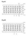
- FIG. 4A is a schematic sectional view that presents semiconductor chips being laminated
- FIG. 4B is a schematic sectional view that presents semiconductor chips being coupled with each other;
- FIG. 5 is a schematic sectional view that presents a microbump before a smooth surface formation process is carried out and the microbump after the smooth surface formation process is carried out;
- FIG. 6 is a flow chart that presents a procedure of the smooth surface formation process (void removal process).
- FIGS. 7A to 7G are schematic sectional views that present the procedure of the smooth surface formation process (void removal process);
- FIGS. 8A to 8G are schematic sectional views that present the procedure of the smooth surface formation process (void removal process) according to a variation
- FIG. 9 is a graph that presents a profile of the temperature and pressure in the heating furnace.
- FIG. 10 is a table that presents experiment results of Examples and Comparative Examples.
- FIG. 1 is a schematic sectional view that presents an embodiment of a semiconductor package.
- a semiconductor package 100 includes a laminate 2 constituted by laminating three or more (it is three here) semiconductor chips 1 , an organic substrate 4 electrically connected with the laminate 2 via a solder ball 3 , and a molded portion 6 formed by covering with a mold resin the laminate 2 mounted on the organic substrate 4 .
- an inner space of the molded portion 6 is filled with an underfill 7 so that gaps between the semiconductor chips 1 of the laminate 2 are filled.
- the laminate 2 is constituted by laminating the semiconductor chip 1 A, the semiconductor chip 1 B, and the semiconductor chip 1 C in a vertical direction.
- the semiconductor chip 1 A and the semiconductor chip 1 B are bonded via a bonded portion 8 bonded by melting the microbump.
- the semiconductor chip 1 C and the semiconductor chip 1 B are bonded via the bonded portion 8 bonded by melting the microbump.
- the semiconductor chips 1 before bonded include a substrate 11 , conductive portions 12 formed on the substrate 11 , and microbumps 13 formed on the conductive portions 12 .
- the substrate 11 is composed of, for instance, a semiconductor chip such as a silicon (Si) chip, a silicon (Si) interposer, and the like.
- the semiconductor chip 1 A and the semiconductor chip 1 C are provided with the conductive portions 12 formed only on one principal surface.
- the semiconductor chip 1 B is provided with the conductive portions 12 formed on both principal surfaces.
- the conductive portions 12 formed on both principal surfaces of the semiconductor chip 1 B are connected to each other via through hole electrodes 19 that extend in a thickness direction of the substrate 11 .
- the plurality of conductive portions 12 are formed on the principal surfaces of the substrate 11 .
- the conductive portions 12 are arranged with a predetermined pitch on the principal surfaces of the substrate 11 .
- the conductive portion 12 includes an electrode pad 14 formed on the principal surface of the substrate 111 and a barrier metal layer 16 formed on an upper surface of the electrode pad 14 . It should be noted that a portion of the principal surface of the substrate 11 on which the conductive portions 12 are not formed is covered with an insulation layer 17 (see FIG. 5 ).
- materials that compose the barrier metal layer 16 for example, Ni, Ni compound (such as NiP), and the like are used.
- materials that compose the insulation layer 17 for instance, SiO, SiN, polyimide and the like are used.
- the microbump 13 is formed on the barrier metal layer 16 of the conductive portion 12 .
- the microbump 13 may include Sn, Ag, Cu, Ag—Cu, Bi, In, and the like as materials that compose the microbump 13 , and an alloy of any two or more of these materials may be used.
- the microbump 13 may include Sn as a principal component.
- the microbump 13 may be formed by plating for example.
- the microbump 13 may be formed by using a micro ball made of a solder alloy, and it may be formed by printing a paste. It should be noted that a bump that is less than 50 ⁇ m in diameter seen from above is referred to as a microbump.
- the microbump 13 has a spherical surface immediately after being formed on the substrate 11 .
- a smooth surface 13 a is formed on the microbump 13 .
- the smooth surface 13 a is constituted with a flat surface extending in a horizontal direction at a top of the microbump 13 . It should be noted that an example of the processing detail for forming the smooth surface 13 a will be described later.
- a height of the microbump 13 in other words, a dimension between the smooth surface 13 a and the upper surface of the conductive portion 12 can be set in a range of 5 to 50 ⁇ m.
- step S 1 a semiconductor chip preparation process in which the semiconductor chip 1 is prepared by forming the microbump 13 on the substrate 11 , is carried out. This prepares the semiconductor chip 1 A, the semiconductor chip 1 B, and the semiconductor chip 1 C. However, in this stage, the smooth surface 13 a has not been formed on the microbump 13 .
- step S 2 a smooth surface formation process (step S 2 ), in which the smooth surface 13 a is formed on the microbump 13 , is carried out.
- the smooth surface formation process S 2 corresponds to a void removal process, in which a void 22 is removed from an inside of the microbump 13 .
- a pressure application member placement process in which a pressure application member 21 is placed on the microbump 13 , is carried out.
- the semiconductor chip 1 is arranged inside of a heating furnace in a state where the pressure application member 21 is placed thereon.
- the subsequent description will be given with reference to a profile of a temperature and pressure in the heating furnace presented in FIG. 9 as appropriate.
- the solid line denotes the temperature in the heating furnace and the dashed line denotes the pressure in the heating furnace.
- a principal surface 21 a that contacts the microbump 13 is preferably constructed as a flat surface. It is because the pressure application member 21 becomes hard to remove because, for example, if a protrusion or the like is formed on the principal surface 21 a , it is caught with the microbump 13 . It is preferable that the only pressure that the pressure application member 21 applies to the microbump 13 is the own weight of the pressure application member 21 itself.
- the pressure is from 0.0005 ⁇ g/ ⁇ m 2 to 0.1 ⁇ g/ ⁇ m 2 per cross-sectional area of the microbump.
- the pressure or the height of the pressure application member 21 is controlled with a method such as flip-chip implementation, the pressure applied to the pressure application member 21 is reduced when the microbump 13 changes from a solid to a liquid (when it changes from FIGS. 7B to 7C ), and hence a misalignment occurs in the position of the pressure application member 21 .
- a slight misalignment causes excessive pressure to be applied.
- a decompression process in which a space in the heating furnace where the semiconductor chips 1 are arranged is decompressed, is carried out.
- inside of the heating furnace is vacuumed so that a reduced-pressure atmosphere is created. Oxygen remaining in the heating furnace causes the microbump 13 to be oxidized. Accordingly, it is preferable that inside of the heating furnace is decompressed to a decompressed state of atmospheric pressure (from 1.01 ⁇ 10 ⁇ 5 Pa to 1 ⁇ 10 ⁇ 3 Pa or less, in particular, 5 Pa or less). This reduces the pressure in the heating furnace (see P 1 portion of the graph of FIG. 9 ). Inert gas is introduced in the heating furnace of the reduced-pressure atmosphere.
- inert gas prevents further oxidization of the surface of the microbump 13 and realizes melting of the microbump 13 , thus functioning as a heating medium in the heating furnace.
- inert gas for example, nitrogen (N 2 ) gas, argon (Ar) gas, and the like can be used.
- a heating process in which reducing gas is caused to flow in the heating furnace in an inert atmosphere and heated at a temperature of melting point or higher of microbump 13 , is carried out.
- the heating process S 22 is carried out after the inert gas is introduced into the heating furnace or substantially simultaneously with introduction of the inert gas.
- the temperature inside the heating furnace is raised at a predetermined rate of temperature rise (for instance 35 to 45° C./minute), and the temperature inside the heating furnace in a state where the inert gas has been introduced is raised to the temperature range of melting point or higher of the microbump 13 .
- the melting point is approximately 220 to 230° C. although depending upon the composition of the alloy, and hence the temperature inside the heating furnace is raised to the temperature range of such temperature or higher.
- the introduction of reducing gas is carried out before or after at the temperature at which a reduction reaction of an oxide film 23 begins. While maintaining the temperature inside the heating furnace (temperature T 1 of FIG. 9 ) at the temperature at which a reduction reaction begins or higher, reducing gas with an appropriate density and flow rate is continued to be supplied. This allows the oxide film 23 existing on the surface of the microbump 13 to be reduced and removed.
- a reducing gas for example, carboxylic acid (formic acid) is applied.
- carboxylic acid include lower carboxylic acid such as formic acid, acetic acid, acrylic acid, and propionic acid.
- formic acid is used as a reducing gas
- it is preferable that formic acid is introduced when the temperature inside the heating furnace becomes about 110° C. Even if formic acid is introduced at a temperature at which a reduction reaction begins or lower, the reaction does not proceed, and if the temperature is too high, the microbump 13 is heated with the oxide film 23 on the surface being left and hence the pressure inside the void 22 rises. Removing the oxide film 23 in a state where the pressure inside the void 22 has excessively risen releases the pressure inside the void 22 all at once and the microbump 13 that has been liquefied may scatter.
- the temperature T 1 at which the reducing reaction begins may be maintained for a predetermined length of time, and in a stage where the oxide film 23 has been sufficiently removed, the temperature of the heating furnace may be maintained at the temperature T 2 , which is the melting point or higher of the microbump 13 (see FIG. 9 ).
- a temperature drop process in which the temperature of the heating furnace is dropped, is carried out. More specifically, in the heating furnace where the temperature T 2 , which is the melting point or higher of the microbump 13 , is maintained, after the microbump 13 is exposed to formic acid for a predetermined length of time (for instance, 0.5 to 3 minutes), the formic acid introduced into the heating furnace is exhausted by vacuuming. After the formic acid introduced into the heating furnace is exhausted or substantially simultaneously with the exhaust of the formic acid, inside the heating furnace is dropped at a predetermined rate of temperature drop (for example, ⁇ 5 to ⁇ 40° C./minute).
- vacuuming is carried out before the temperature in the heating furnace is dropped.
- an inert gas such as nitrogen gas and argon gas may be introduced into the heating furnace to return to the atmospheric pressure.
- the void 22 is removed from the microbump 13 and the smooth surface 13 a is formed on the microbump 13 .
- the oxide film 23 formed on the surface of the microbump 13 is reduced and removed (see FIG. 7B ).
- the microbump 13 is molten.
- the pressure of the pressure application member 21 deforms the microbump 13 as if it is collapsed.
- a shape corresponding to the smooth surface 13 a is formed on the microbump 13 (see FIGS. 7C to 7F ).
- the microbump 13 that has been molten is pushed by the pressure application member 21 and flows, and thus the void 22 in the microbump 13 rises and escapes to outside (see FIGS. 7C to 7F ).
- the microbump 13 is cooled and hardened.
- the smooth surface 13 a is formed on the microbump 13 (see FIG. 7G ).
- a lamination process in which three or more of the semiconductor chips 1 are laminated by overlaying the microbump 13 of one of the semiconductor chips 1 on the microbump 13 of another one of the semiconductor chips 1 , is carried out.
- the smooth surface 13 a is formed on the microbump 13 of one of the semiconductor chips 1 and another one of the semiconductor chips 1 .
- the microbump 13 of one of the semiconductor chips 1 contacts the microbump 13 of another one of the semiconductor chips 1 on the smooth surface 13 a .
- all the semiconductor chips 1 are overlaid in a state where the microbumps 13 are not bonded to each other.
- the microbump 13 of the semiconductor chip 1 B is overlaid on the microbump 13 of the semiconductor chip 1 C, which is the bottommost.
- the smooth surface 13 a of the microbump 13 of the semiconductor chip 1 B is overlaid on the smooth surface 13 a of the microbump 13 of the semiconductor chip 1 C.
- the microbump 13 of the semiconductor chip 1 C and the microbump 13 of the semiconductor chip 1 B are not bonded to each other, and they are in a state of simply contacting each other.
- the microbump 13 of the semiconductor chip 1 A which is the uppermost, is overlaid on the microbump 13 of the semiconductor chip 1 B, which is the second from the bottom.
- the smooth surface 13 a of the microbump 13 of the semiconductor chip 1 A is overlaid on the smooth surface 13 a of the microbump 13 of the semiconductor chip 1 B.
- the microbump 13 of the semiconductor chip 1 B and the microbump 13 of the semiconductor chip 1 A are not bonded to each other, and they are in a state of simply contacting each other.
- step S 4 a bonding process in which the semiconductor chips 1 are bonded to each other via the microbumps 13 by heating to melt the microbumps 13 , is carried out.
- the bonding process S 4 all the microbumps 13 are collectively molten by heating once and all the semiconductor chips 1 are collectively bonded.
- the microbumps 13 of the semiconductor chips 1 are molten in a reducing atmosphere.
- a lamination in a state where the semiconductor chip 1 A, the semiconductor chip 1 B, and the semiconductor chip 1 C are laminated via the microbumps 13 is arranged in the heating furnace. Then, by heating the lamination in the heating furnace, all the microbumps 13 in the lamination are molten and the microbumps 13 that have been contact each other are collectively bonded. Thus, the semiconductor chip 1 A, the semiconductor chip 1 B, and the semiconductor chip 1 C are bonded via the bonded portion 8 at which two of the microbumps 13 are molten and bonded to each other, as presented in FIG. 4B .
- a semiconductor package creation process in which the semiconductor package 100 is created, is carried out.
- the laminate 2 which is obtained in the bonding process S 4 , is coupled to the organic substrate 4 , and the laminate 2 is covered with the molded portion 6 .
- the semiconductor package 100 is completed and the method for producing presented in FIG. 2 terminates.
- the reducing gas is caused to flow in an inert atmosphere into a space where the semiconductor chips 1 are arranged.
- the oxide film 23 formed on a surface of the microbump 13 is reduced and removed.
- heated at or higher than a temperature of the melting point of the microbump 13 and thus the microbump 13 gets fluidity by being molten.
- the pressure application member 21 is mounted on the microbump 13 . Accordingly, as the microbump 13 is molten and gets fluidity, pressure of the pressure application member 21 causes the microbump 13 to be deformed as if it is collapsed.
- the deformation generates a flow in the microbump 13 and the void 22 flows in the microbump 13 .
- the void 22 flowing in the microbump 13 escapes from the microbump 13 to outside and is removed.
- the void 22 in the microbump 13 can be removed with ease.
- carboxylic acid may be applied.
- the oxide film 23 on the surface of the microbump 13 is removed successfully.
- the weight of the pressure application member 21 may be from 0.0005 ⁇ g/ ⁇ m 2 to 0.1 ⁇ g/ ⁇ m 2 per cross-sectional area of the microbump 13 .
- the pressure application member 21 is capable of applying an appropriate pressure to remove the void 22 on the microbump 13 .
- the smooth surface 13 a is formed on the microbump 13 of at least one of them, and the microbump 13 of one of them contacts the microbump 13 of the other one of them on the smooth surface 13 a .
- one of the semiconductor chips 1 and the other one of the semiconductor chips 1 can be laminated with accurate positioning. This allows even a multitude of semiconductor chips 1 of three or more to be laminated in a state with accurate positioning between the semiconductor chips 1 .
- the bonding process S 4 By carrying out the bonding process S 4 in this state, the semiconductor chip 1 and the semiconductor chip 1 can be bonded with accurate positioning.
- Both the microbump 13 of one of the semiconductor chips 1 and the microbump 13 of another one of the semiconductor chips 1 contain Sn, and in the bonding process S 4 , the microbump 13 of one of the semiconductor chips 1 and the microbump 13 of another one of the semiconductor chips 1 may be molten in a reducing atmosphere. Thus, the oxide film 23 formed on the surface of the microbumps 13 of each other is reduced and removed. In addition, since the microbumps 13 of each other contain Sn, they are mixed with each other and integrated with melting. With this, by an action of surface tension of the microbump 13 that has been liquefied, a position misalignment between one of the semiconductor chips 1 and the other one of the semiconductor chips 1 (self-alignment effect).
- the smooth surface formation process S 2 includes the heating process S 22 , in which a reducing gas is caused to flow in an inert atmosphere with respect to the space where the semiconductor chips 1 are arranged and heated at a temperature of melting point or higher of the microbump 13 so that the oxide film 23 on the surface of the microbump 13 is removed, and in the heating process S 22 , the pressure application member 21 may be mounted on the microbump 13 .
- a reducing gas is caused to flow in an inert atmosphere with respect to the space where the semiconductor chips 1 are arranged and heated at a temperature of melting point or higher of the microbump 13 so that the oxide film 23 on the surface of the microbump 13 is removed.
- the pressure application member 21 is mounted on the microbump 13 . Accordingly, as the microbump 13 is molten and gets fluidity, pressure of the pressure application member 21 causes the microbump 13 to be deformed as if it is collapsed. The deformation generates a flow in the microbump 13 and the void 22 flows in the microbump 13 . Thus, the void 22 flowing in the microbump 13 escapes from the microbump 13 to outside and the void 22 is removed.
- a portion pushed by the pressure application member 21 is formed as the smooth surface 13 a in accordance with the shape of the pressure application member 21 .
- the present invention is not to be limited to the embodiment described above.
- a spacer 26 that has a certain thickness is arranged on the substrate 11 and the pressure application member 21 may be pushed to contact the spacer 26 .
- the spacers 26 are arranged on the both sides of the microbump 13 and the pressure application member 21 is mounted on the microbump 13 (see FIG. 8A ).
- heated in a reducing atmosphere and the oxide film is removed (see FIG. 8B ).
- the pressure application member 21 drops and contacts the upper surface of the spacer 26 (see FIG. 8C ).
- the pressure application member 21 is supported by the spacer 26 and does not drop any further.
- a flow is generated due to an impact of the pressure application member 21 and the void 22 rises and is removed (see FIGS. 8D to 8G ).
- the microbump 13 of the semiconductor chip 1 of the lower side has the smooth surface 13 a and the microbump 13 of the semiconductor chip 1 of the upper side has the smooth surface 13 a . Accordingly, the smooth surface 13 a of the microbump 13 of the upper side is mounted on the smooth surface 13 a of the microbump 13 of the lower side.
- the smooth surface 13 a may be formed on any one of the microbump 13 of the upper side and the microbump 13 of the lower side and the smooth surface 13 a may not be formed on the other side.
- the smooth surface 13 a may be formed in any method.
- the smooth surface 13 a may be formed by grinding the microbump 13 .
- the smooth surface 13 a is formed by grinding, there is a possibility of damage being caused by force acting on the microbump 13 and the conductive portion 12 .
- the smooth surface 13 a is formed by using the pressure application member 21 as in the embodiment described above, damage on the microbump 13 and the conductive portion 12 can be suppressed.
- Example 1 a semiconductor chip that includes a microbump as follows was produced. First, a substrate was provided with Cu plating, Ni plating, and Sn plating using an electrolytic plating process. After this was arranged in a heating furnace, an atmosphere pressure in the heating furnace was adjusted and density and flow rate of nitrogen and formic acid gas to be supplied to the heating furnace were adjusted. This caused a sample of the semiconductor chip on which a plating film was molten and the microbump was formed to be created. The Cu plating layer is 17 ⁇ m high, the Ni plating layer is 3 ⁇ m high, the microbump is 15 ⁇ m high, and the microbump is 35 ⁇ m in diameter. This sample and a pressure application member were prepared.
- the pressure application member was an Si wafer that includes an SiO 2 film.
- the Si wafer was mounted on the microbump so that the SiO 2 surface contacted the microbump.
- the weight of the pressure application member was 0.0005 ⁇ g/ ⁇ m 2 per cross-sectional area of the microbump. It should be noted that the spacer as presented in FIG. 8 was not provided. After the semiconductor chip in a state where the pressure application member was mounted thereon was arranged in the heating furnace, inside of the heating furnace was vacuumed to 5 Pa or less. A subsequent atmosphere pressure in the heating furnace was adjusted and density and flow rate of nitrogen and formic acid gas to be supplied to the heating furnace were adjusted.
- Example 2 One in which reflow was carried out in an atmosphere of nitrogen and formic acid at the time of bonding the semiconductor chips to each other was Example 2.
- Example 3 One with 5 semiconductor chips laminated was Example 3.
- Example 4 One with 5 semiconductor chips laminated in which reflow was carried out in an atmosphere of nitrogen and formic acid at the time of bonding the semiconductor chips to each other was Example 4. All of the other conditions of Examples 2 to 4 were the same as those of Example 1.
- Comparative Example 1 One with the microbumps with no smooth surface formed thereon overlaid was Comparative Example 1.
- Comparative Example 2 One with 5 semiconductor chips laminated and with the microbumps with no smooth surface formed thereon overlaid was Comparative Example 2. All of the other conditions of Comparative Examples 1 and 2 were the same as those of Example 1.
- a position gap of the center of the microbump of the first and second semiconductor chips when the third semiconductor chip was overlaid was measured.
- Examples 1 to 4 and Comparative Examples 1 and 2 those with a position gap of less than 5 ⁇ m are provided with “o” and those with 5 ⁇ m or greater are provided with “x” in “Lamination Accuracy” of FIG. 10 .
- the substrate and the substrate were separated.
- Examples 1 to 4 and Comparative Examples 1 and 2 those with fracture inside the microbump are provided with “o” and those with separation or crack on the interface between the microbump and the Ni plated layer are provided with “x” in “Bump Separation Mode” of FIG.
- Comparative Example 1 the bottom chip was misaligned when the third chip was overlaid. In other words, Comparative Example 1 indicates a low lamination accuracy and accordingly has a reduced bonding accuracy. In Comparative Example 2, bonding in a one-by-one basis improved the lamination accuracy and the bonding accuracy. However, Comparative Example 2 indicates that repeated reflow resulted in growth of the alloy layer of Ni and Sn, thereby reducing the strength of the bonded portion. Example 1 indicates that there is little misalignment when the microbumps are overlaid because they have the smooth surface, and thus the bonding accuracy is high.
- Example 2 the oxide film is removed by carrying out reflow in a reducing atmosphere, and the bonding accuracy was further improved due to the effect of self alignment of surface tension of molten Sn.
- Examples 3 and 4 indicate that there is little reduction in the strength of the bonded portion because reflow is carried out once.
Abstract
A method for producing a semiconductor package in which a plurality of semiconductor chips, each of which includes a substrate, conductive portions formed on the substrate, and microbumps formed on the conductive portions, are laminated, which includes a smooth surface formation process of forming a smooth surface on the microbump, a lamination process of laminating three or more of the semiconductor chips by overlaying the microbump of one of the semiconductor chips on the microbump of another one of the semiconductor chips, and a bonding process of bonding the semiconductor chips to each other via the microbumps by heating to melt the microbumps, in which in the lamination process, of one of the semiconductor chips and another one of the semiconductor chips, the smooth surface is formed on at least one of the microbump, and one of the microbump contacts another one of the microbump on the smooth surface.
Description
The present invention relates to a method for producing a semiconductor package.
Conventionally, in a three-dimensional installation of semiconductor package, coupling between a semiconductor chip and a semiconductor chip or an interposer is performed by wire bonding. In place of the wire bonding, a three-dimensional installation technique, with which semiconductor chips are coupled with each other via a pass-through electrode and a bump, has been developed. The pass-through electrode normally has a short connecting wire length (for example, 50 μm), and a bump, via which electrodes are connected, is also required to be microscopic. A technique that handles such a bump pitch of less than 50 μm is referred to as a microbump. As U.S. Pat. No. 9,136,159, a wiring length between semiconductor chips can be dramatically shortened by coupling the semiconductor chip and the semiconductor chip with the pass-through electrode and the microbump. Accordingly, a wiring delay time that increases with miniaturization can be reduced.
Here, lamination of a semiconductor chip and the semiconductor chip is carried out by flip-chip implementation. However, as a plurality of the semiconductor chips are laminated and bonded, problems such as a position misalignment between the semiconductor chips occur.
Made in consideration of such a circumstance, the present invention is intended to provide a method for producing a semiconductor package in which the semiconductor chip and the semiconductor chip can be bonded with accurate positioning.
A method for producing a semiconductor package according to an aspect of the present invention is a method for producing a semiconductor package in which a plurality of semiconductor chips, each of which includes a substrate, a conductive portion formed on the substrate, and a microbump formed on the conductive portion, are laminated, which includes a smooth surface formation process of forming a smooth surface on the microbump, a lamination process of laminating three or more of the semiconductor chips by overlaying the microbump of one of the semiconductor chips on the microbump of another one of the semiconductor chips, and a bonding process of bonding the semiconductor chips to each other via the microbumps by heating to melt the microbumps, in which in the lamination process, of one of the semiconductor chips and another one of the semiconductor chips, the smooth surface is formed on at least one of the microbump, and one of the microbump contacts another one of the microbump on the smooth surface.
In the method for producing the semiconductor package, in the lamination process, of one of the semiconductor chips and another one of the semiconductor chips, the smooth surface is formed on at least one of the microbump, and one of the microbump contacts another one of the microbump on the smooth surface. In this manner, by overlaying the microbumps of each other using the smooth surface, one of the semiconductor chips and the other one of the semiconductor chips can be laminated with accurate positioning. This allows even a multitude of semiconductor chips of three or more to be laminated in a state with accurate positioning between the semiconductor chips. By carrying out the bonding process in this state, the semiconductor chip and the semiconductor chip can be bonded with accurate positioning.
In the lamination process, all the semiconductor chips are overlaid in a state where the microbumps are not bonded to each other, and in the bonding process, all the microbumps may be collectively molten by heating once and all the semiconductor chips may be collectively bonded. This can prevent the bonded portion, which has been bonded by melting the microbump once, from being repeatedly heated. Accordingly, reduction of the strength of the bonded portion can be prevented.
Both the microbump of one of the semiconductor chips and the microbump of another one of the semiconductor chips contain Sn, and in the bonding process, the microbump of one of the semiconductor chips and the microbump of another one of the semiconductor chips may be molten in a reducing atmosphere. Thus, the oxide film formed on the surface of the microbumps of each other is reduced and removed. In addition, since the microbumps of each other contain Sn, they are mixed with each other and integrated with melting. With this, by an action of surface tension of the microbump that has been liquefied, a position misalignment between one of the semiconductor chips and the other one of the semiconductor chips (self-alignment effect).
The smooth surface formation process includes a heating process of causing a reducing gas to flow in an inert atmosphere with respect to the space where the semiconductor chips are arranged and applying heat at a temperature of melting point or higher of the microbump, and in the heating process, a pressure application member may be mounted on the microbump. In the heating process, the reducing gas is caused to flow in an inert atmosphere into a space where the semiconductor chips are arranged. Thus, an oxide film formed on a surface of the microbump is reduced and removed. In addition, in the heating process, heated at or higher than a temperature of the melting point of the microbump, and thus the microbump is molten and gets fluidity. Here, in the heating process, the pressure application member is mounted on the microbump. Accordingly, as the microbump is molten and gets fluidity, pressure of the pressure application member causes the microbump to be deformed as if it is collapsed. The deformation generates a flow in the microbump and the void flows in the microbump. Thus the void flowing in the microbump escapes from the microbump to outside and the void is removed. In addition, in the microbump that has been molten, a portion pushed by the pressure application member is formed as the smooth surface in accordance with the shape of the pressure application member.
According to the present invention, a method for producing a semiconductor package in which a semiconductor chip and a semiconductor chip can be bonded with accurate positioning can be provided.
Now, preferred embodiments of a method for producing a semiconductor package according to an aspect of the present invention will be described in detail with reference to the drawings. It should be noted that elements that are identical or elements that have an identical function are designated by the same reference numerals, and redundant descriptions will be curtailed.
For example, as presented in FIG. 4A , the semiconductor chips 1 before bonded include a substrate 11, conductive portions 12 formed on the substrate 11, and microbumps 13 formed on the conductive portions 12. The substrate 11 is composed of, for instance, a semiconductor chip such as a silicon (Si) chip, a silicon (Si) interposer, and the like. It should be noted that the semiconductor chip 1A and the semiconductor chip 1C are provided with the conductive portions 12 formed only on one principal surface. The semiconductor chip 1B is provided with the conductive portions 12 formed on both principal surfaces. In addition, the conductive portions 12 formed on both principal surfaces of the semiconductor chip 1B are connected to each other via through hole electrodes 19 that extend in a thickness direction of the substrate 11.
The plurality of conductive portions 12 are formed on the principal surfaces of the substrate 11. The conductive portions 12 are arranged with a predetermined pitch on the principal surfaces of the substrate 11. The conductive portion 12 includes an electrode pad 14 formed on the principal surface of the substrate 111 and a barrier metal layer 16 formed on an upper surface of the electrode pad 14. It should be noted that a portion of the principal surface of the substrate 11 on which the conductive portions 12 are not formed is covered with an insulation layer 17 (see FIG. 5 ). As materials that compose the barrier metal layer 16, for example, Ni, Ni compound (such as NiP), and the like are used. As materials that compose the insulation layer 17, for instance, SiO, SiN, polyimide and the like are used.
The microbump 13 is formed on the barrier metal layer 16 of the conductive portion 12. The microbump 13 may include Sn, Ag, Cu, Ag—Cu, Bi, In, and the like as materials that compose the microbump 13, and an alloy of any two or more of these materials may be used. In particular, the microbump 13 may include Sn as a principal component. The microbump 13 may be formed by plating for example. Alternatively, the microbump 13 may be formed by using a micro ball made of a solder alloy, and it may be formed by printing a paste. It should be noted that a bump that is less than 50 μm in diameter seen from above is referred to as a microbump.
As presented in FIG. 5 , the microbump 13 has a spherical surface immediately after being formed on the substrate 11. By providing a predetermined processing to the microbump 13, a smooth surface 13 a is formed on the microbump 13. The smooth surface 13 a is constituted with a flat surface extending in a horizontal direction at a top of the microbump 13. It should be noted that an example of the processing detail for forming the smooth surface 13 a will be described later. A height of the microbump 13, in other words, a dimension between the smooth surface 13 a and the upper surface of the conductive portion 12 can be set in a range of 5 to 50 μm.
Next, a method for producing the semiconductor package 100 according to the present embodiment will be described with reference to FIGS. 2 to 9 .
As presented in FIG. 2 , first, a semiconductor chip preparation process (step S1), in which the semiconductor chip 1 is prepared by forming the microbump 13 on the substrate 11, is carried out. This prepares the semiconductor chip 1A, the semiconductor chip 1B, and the semiconductor chip 1C. However, in this stage, the smooth surface 13 a has not been formed on the microbump 13.
Next, a smooth surface formation process (step S2), in which the smooth surface 13 a is formed on the microbump 13, is carried out. In addition, the smooth surface formation process S2 corresponds to a void removal process, in which a void 22 is removed from an inside of the microbump 13.
A detail of the smooth surface formation process (void removal process) S2 will now be described with reference to FIG. 6 .
As presented in FIGS. 6 and 7A , a pressure application member placement process (step S20), in which a pressure application member 21 is placed on the microbump 13, is carried out. In this manner, the semiconductor chip 1 is arranged inside of a heating furnace in a state where the pressure application member 21 is placed thereon. It should be noted that the subsequent description will be given with reference to a profile of a temperature and pressure in the heating furnace presented in FIG. 9 as appropriate. It should be noted that in FIG. 9 , the solid line denotes the temperature in the heating furnace and the dashed line denotes the pressure in the heating furnace.
As materials that compose the pressure application member 21 mounted on the microbump 13, it is preferable that materials that do not react with the microbump 13 are adopted. For instance, Si, SiO2, SiN, and the like are adopted as materials that compose the pressure application member 21. In addition, among the principal surfaces of the pressure application member 21, a principal surface 21 a that contacts the microbump 13 is preferably constructed as a flat surface. It is because the pressure application member 21 becomes hard to remove because, for example, if a protrusion or the like is formed on the principal surface 21 a, it is caught with the microbump 13. It is preferable that the only pressure that the pressure application member 21 applies to the microbump 13 is the own weight of the pressure application member 21 itself. More specifically, it is preferable that the pressure is from 0.0005 μg/μm2 to 0.1 μg/μm2 per cross-sectional area of the microbump. For instance, if the pressure or the height of the pressure application member 21 is controlled with a method such as flip-chip implementation, the pressure applied to the pressure application member 21 is reduced when the microbump 13 changes from a solid to a liquid (when it changes from FIGS. 7B to 7C ), and hence a misalignment occurs in the position of the pressure application member 21. With respect to a small bump such as the microbump 13, a slight misalignment causes excessive pressure to be applied.
Next, a decompression process (step S21), in which a space in the heating furnace where the semiconductor chips 1 are arranged is decompressed, is carried out. In the decompression process S21, inside of the heating furnace is vacuumed so that a reduced-pressure atmosphere is created. Oxygen remaining in the heating furnace causes the microbump 13 to be oxidized. Accordingly, it is preferable that inside of the heating furnace is decompressed to a decompressed state of atmospheric pressure (from 1.01×10^5 Pa to 1×10^3 Pa or less, in particular, 5 Pa or less). This reduces the pressure in the heating furnace (see P1 portion of the graph of FIG. 9 ). Inert gas is introduced in the heating furnace of the reduced-pressure atmosphere. This raises the pressure in the heating furnace (see P2 portion of the graph of FIG. 9 ). When the temperature inside the heating furnace is raised to a temperature range of melting temperature or higher (melting point or higher) of the microbump 13, inert gas prevents further oxidization of the surface of the microbump 13 and realizes melting of the microbump 13, thus functioning as a heating medium in the heating furnace. As such inert gas, for example, nitrogen (N2) gas, argon (Ar) gas, and the like can be used.
Next, a heating process (step S22), in which reducing gas is caused to flow in the heating furnace in an inert atmosphere and heated at a temperature of melting point or higher of microbump 13, is carried out. The heating process S22 is carried out after the inert gas is introduced into the heating furnace or substantially simultaneously with introduction of the inert gas. In the heating process S22, the temperature inside the heating furnace is raised at a predetermined rate of temperature rise (for instance 35 to 45° C./minute), and the temperature inside the heating furnace in a state where the inert gas has been introduced is raised to the temperature range of melting point or higher of the microbump 13. For example, when the bump is composed of Sn—Ag—Cu alloy, the melting point is approximately 220 to 230° C. although depending upon the composition of the alloy, and hence the temperature inside the heating furnace is raised to the temperature range of such temperature or higher.
It is preferable that the introduction of reducing gas is carried out before or after at the temperature at which a reduction reaction of an oxide film 23 begins. While maintaining the temperature inside the heating furnace (temperature T1 of FIG. 9 ) at the temperature at which a reduction reaction begins or higher, reducing gas with an appropriate density and flow rate is continued to be supplied. This allows the oxide film 23 existing on the surface of the microbump 13 to be reduced and removed. As a reducing gas, for example, carboxylic acid (formic acid) is applied. Examples of carboxylic acid include lower carboxylic acid such as formic acid, acetic acid, acrylic acid, and propionic acid. If formic acid is used as a reducing gas, it is preferable that formic acid is introduced when the temperature inside the heating furnace becomes about 110° C. Even if formic acid is introduced at a temperature at which a reduction reaction begins or lower, the reaction does not proceed, and if the temperature is too high, the microbump 13 is heated with the oxide film 23 on the surface being left and hence the pressure inside the void 22 rises. Removing the oxide film 23 in a state where the pressure inside the void 22 has excessively risen releases the pressure inside the void 22 all at once and the microbump 13 that has been liquefied may scatter. Accordingly, the temperature T1 at which the reducing reaction begins may be maintained for a predetermined length of time, and in a stage where the oxide film 23 has been sufficiently removed, the temperature of the heating furnace may be maintained at the temperature T2, which is the melting point or higher of the microbump 13 (see FIG. 9 ).
When the microbump 13 has been molten, the void 22 has been removed, and the smooth surface 13 a has been formed, a temperature drop process (step S23), in which the temperature of the heating furnace is dropped, is carried out. More specifically, in the heating furnace where the temperature T2, which is the melting point or higher of the microbump 13, is maintained, after the microbump 13 is exposed to formic acid for a predetermined length of time (for instance, 0.5 to 3 minutes), the formic acid introduced into the heating furnace is exhausted by vacuuming. After the formic acid introduced into the heating furnace is exhausted or substantially simultaneously with the exhaust of the formic acid, inside the heating furnace is dropped at a predetermined rate of temperature drop (for example, −5 to −40° C./minute). It should be noted that in FIG. 9 , vacuuming is carried out before the temperature in the heating furnace is dropped. However, when the temperature in the heating furnace is dropped to a temperature range where molten bump is solidified to some extent, an inert gas such as nitrogen gas and argon gas may be introduced into the heating furnace to return to the atmospheric pressure.
By carrying out the heating process S22 and the temperature drop process S23 as described above, as presented in FIGS. 7B to 7G , the void 22 is removed from the microbump 13 and the smooth surface 13 a is formed on the microbump 13. In other words, by carrying out heating in an atmosphere of reducing gas, the oxide film 23 formed on the surface of the microbump 13 is reduced and removed (see FIG. 7B ). Then, by applying heat at a temperature of the melting point of the microbump 13 or higher, the microbump 13 is molten. Thus, the pressure of the pressure application member 21 deforms the microbump 13 as if it is collapsed. Due to this, in accordance with the shape of the principal surface 21 a of the pressure application member 21, a shape corresponding to the smooth surface 13 a is formed on the microbump 13 (see FIGS. 7C to 7F ). In addition, the microbump 13 that has been molten is pushed by the pressure application member 21 and flows, and thus the void 22 in the microbump 13 rises and escapes to outside (see FIGS. 7C to 7F ). By returning the temperature in the heating furnace, the microbump 13 is cooled and hardened. Thus, the smooth surface 13 a is formed on the microbump 13 (see FIG. 7G ).
Returning to FIG. 2 , after the smooth surface formation process S2 has been completed with regard to each of the semiconductor chips 1, a lamination process (step S3), in which three or more of the semiconductor chips 1 are laminated by overlaying the microbump 13 of one of the semiconductor chips 1 on the microbump 13 of another one of the semiconductor chips 1, is carried out. In the present embodiment, in the lamination process S3, the smooth surface 13 a is formed on the microbump 13 of one of the semiconductor chips 1 and another one of the semiconductor chips 1. Then, the microbump 13 of one of the semiconductor chips 1 contacts the microbump 13 of another one of the semiconductor chips 1 on the smooth surface 13 a. In the lamination process S3, all the semiconductor chips 1 are overlaid in a state where the microbumps 13 are not bonded to each other.
More specifically, as presented in FIGS. 3A and 3B , the microbump 13 of the semiconductor chip 1B is overlaid on the microbump 13 of the semiconductor chip 1C, which is the bottommost. At this time, the smooth surface 13 a of the microbump 13 of the semiconductor chip 1B is overlaid on the smooth surface 13 a of the microbump 13 of the semiconductor chip 1C. In addition, the microbump 13 of the semiconductor chip 1C and the microbump 13 of the semiconductor chip 1B are not bonded to each other, and they are in a state of simply contacting each other.
Next, as presented in FIGS. 3B and 4A , the microbump 13 of the semiconductor chip 1A, which is the uppermost, is overlaid on the microbump 13 of the semiconductor chip 1B, which is the second from the bottom. At this time, the smooth surface 13 a of the microbump 13 of the semiconductor chip 1A is overlaid on the smooth surface 13 a of the microbump 13 of the semiconductor chip 1B. In addition, the microbump 13 of the semiconductor chip 1B and the microbump 13 of the semiconductor chip 1A are not bonded to each other, and they are in a state of simply contacting each other.
After completing the lamination process S3, a bonding process (step S4), in which the semiconductor chips 1 are bonded to each other via the microbumps 13 by heating to melt the microbumps 13, is carried out. In the bonding process S4, all the microbumps 13 are collectively molten by heating once and all the semiconductor chips 1 are collectively bonded. In addition, in the bonding process S4, the microbumps 13 of the semiconductor chips 1 are molten in a reducing atmosphere.
More specifically, as presented in FIG. 4A , a lamination in a state where the semiconductor chip 1A, the semiconductor chip 1B, and the semiconductor chip 1C are laminated via the microbumps 13 is arranged in the heating furnace. Then, by heating the lamination in the heating furnace, all the microbumps 13 in the lamination are molten and the microbumps 13 that have been contact each other are collectively bonded. Thus, the semiconductor chip 1A, the semiconductor chip 1B, and the semiconductor chip 1C are bonded via the bonded portion 8 at which two of the microbumps 13 are molten and bonded to each other, as presented in FIG. 4B .
After completing the bonding process S4, a semiconductor package creation process (step S5), in which the semiconductor package 100 is created, is carried out. In the semiconductor package creation process S5, the laminate 2, which is obtained in the bonding process S4, is coupled to the organic substrate 4, and the laminate 2 is covered with the molded portion 6. With above, the semiconductor package 100 is completed and the method for producing presented in FIG. 2 terminates.
Next, an operation and effect of the method for producing the semiconductor package 100 according to the present embodiment will be described.
In the method for producing the semiconductor package 100, in the heating process S22, the reducing gas is caused to flow in an inert atmosphere into a space where the semiconductor chips 1 are arranged. Thus, the oxide film 23 formed on a surface of the microbump 13 is reduced and removed. In addition, heated at or higher than a temperature of the melting point of the microbump 13, and thus the microbump 13 gets fluidity by being molten. Here, in the heating process S22, the pressure application member 21 is mounted on the microbump 13. Accordingly, as the microbump 13 is molten and gets fluidity, pressure of the pressure application member 21 causes the microbump 13 to be deformed as if it is collapsed. The deformation generates a flow in the microbump 13 and the void 22 flows in the microbump 13. Thus, the void 22 flowing in the microbump 13 escapes from the microbump 13 to outside and is removed. With above, the void 22 in the microbump 13 can be removed with ease.
As the reducing gas, carboxylic acid may be applied. Thus, the oxide film 23 on the surface of the microbump 13 is removed successfully.
The weight of the pressure application member 21 may be from 0.0005 μg/μm2 to 0.1 μg/μm2 per cross-sectional area of the microbump 13. Thus, the pressure application member 21 is capable of applying an appropriate pressure to remove the void 22 on the microbump 13.
In the method for producing the semiconductor package 100, in the lamination process S3, of one of the semiconductor chips 1 and another one of the semiconductor chips 1, the smooth surface 13 a is formed on the microbump 13 of at least one of them, and the microbump 13 of one of them contacts the microbump 13 of the other one of them on the smooth surface 13 a. In this manner, by overlaying the microbumps 13 of each other using the smooth surface 13 a, one of the semiconductor chips 1 and the other one of the semiconductor chips 1 can be laminated with accurate positioning. This allows even a multitude of semiconductor chips 1 of three or more to be laminated in a state with accurate positioning between the semiconductor chips 1. By carrying out the bonding process S4 in this state, the semiconductor chip 1 and the semiconductor chip 1 can be bonded with accurate positioning.
In the lamination process S3, all the semiconductor chips 1 are overlaid in a state where the microbumps 13 are not bonded to each other, and in the bonding process S4, all the microbumps 13 are collectively molten by heating once and all the semiconductor chips 1 are collectively bonded. This can prevent the bonded portion 8, which has been bonded by melting the microbump 13 once, from being repeatedly heated. Accordingly, reduction of the strength of the bonded portion 8 can be prevented.
Both the microbump 13 of one of the semiconductor chips 1 and the microbump 13 of another one of the semiconductor chips 1 contain Sn, and in the bonding process S4, the microbump 13 of one of the semiconductor chips 1 and the microbump 13 of another one of the semiconductor chips 1 may be molten in a reducing atmosphere. Thus, the oxide film 23 formed on the surface of the microbumps 13 of each other is reduced and removed. In addition, since the microbumps 13 of each other contain Sn, they are mixed with each other and integrated with melting. With this, by an action of surface tension of the microbump 13 that has been liquefied, a position misalignment between one of the semiconductor chips 1 and the other one of the semiconductor chips 1 (self-alignment effect).
The smooth surface formation process S2 includes the heating process S22, in which a reducing gas is caused to flow in an inert atmosphere with respect to the space where the semiconductor chips 1 are arranged and heated at a temperature of melting point or higher of the microbump 13 so that the oxide film 23 on the surface of the microbump 13 is removed, and in the heating process S22, the pressure application member 21 may be mounted on the microbump 13. In the heating process S22, a reducing gas is caused to flow in an inert atmosphere with respect to the space where the semiconductor chips 1 are arranged and heated at a temperature of melting point or higher of the microbump 13 so that the oxide film 23 on the surface of the microbump 13 is removed. Thus, the oxide film 23 formed on the surface of the microbump 13 to be reduced and removed, and the microbump 13 gets fluidity by being molten. Here, in the heating process S22, the pressure application member 21 is mounted on the microbump 13. Accordingly, as the microbump 13 is molten and gets fluidity, pressure of the pressure application member 21 causes the microbump 13 to be deformed as if it is collapsed. The deformation generates a flow in the microbump 13 and the void 22 flows in the microbump 13. Thus, the void 22 flowing in the microbump 13 escapes from the microbump 13 to outside and the void 22 is removed. In addition, in the microbump 13 that has been molten, a portion pushed by the pressure application member 21 is formed as the smooth surface 13 a in accordance with the shape of the pressure application member 21.
The present invention is not to be limited to the embodiment described above.
For instance, as presented in FIG. 8 , a spacer 26 that has a certain thickness is arranged on the substrate 11 and the pressure application member 21 may be pushed to contact the spacer 26. This causes the spacer 26 to stop the pressure application member 21 and thus can prevent the microbump 13 from being collapsed too much. For example, before heated, the spacers 26 are arranged on the both sides of the microbump 13 and the pressure application member 21 is mounted on the microbump 13 (see FIG. 8A ). In this state, heated in a reducing atmosphere and the oxide film is removed (see FIG. 8B ). The, when the microbump 13 is molten, the pressure application member 21 drops and contacts the upper surface of the spacer 26 (see FIG. 8C ). Thus, the pressure application member 21 is supported by the spacer 26 and does not drop any further. On the other hand, in the microbump 13 that has been molten, a flow is generated due to an impact of the pressure application member 21 and the void 22 rises and is removed (see FIGS. 8D to 8G ).
In addition, in the embodiment described above, the microbump 13 of the semiconductor chip 1 of the lower side has the smooth surface 13 a and the microbump 13 of the semiconductor chip 1 of the upper side has the smooth surface 13 a. Accordingly, the smooth surface 13 a of the microbump 13 of the upper side is mounted on the smooth surface 13 a of the microbump 13 of the lower side. However, the smooth surface 13 a may be formed on any one of the microbump 13 of the upper side and the microbump 13 of the lower side and the smooth surface 13 a may not be formed on the other side.
It should be noted that in the smooth surface formation process of the microbump 13, the smooth surface 13 a may be formed in any method. For example, the smooth surface 13 a may be formed by grinding the microbump 13. However, when the smooth surface 13 a is formed by grinding, there is a possibility of damage being caused by force acting on the microbump 13 and the conductive portion 12. On the other hand, if the smooth surface 13 a is formed by using the pressure application member 21 as in the embodiment described above, damage on the microbump 13 and the conductive portion 12 can be suppressed.
Examples of the present invention will be described next. However, the present invention is not to be limited to the Examples described below.
As Example 1, a semiconductor chip that includes a microbump as follows was produced. First, a substrate was provided with Cu plating, Ni plating, and Sn plating using an electrolytic plating process. After this was arranged in a heating furnace, an atmosphere pressure in the heating furnace was adjusted and density and flow rate of nitrogen and formic acid gas to be supplied to the heating furnace were adjusted. This caused a sample of the semiconductor chip on which a plating film was molten and the microbump was formed to be created. The Cu plating layer is 17 μm high, the Ni plating layer is 3 μm high, the microbump is 15 μm high, and the microbump is 35 μm in diameter. This sample and a pressure application member were prepared. The pressure application member was an Si wafer that includes an SiO2 film. The Si wafer was mounted on the microbump so that the SiO2 surface contacted the microbump. The weight of the pressure application member was 0.0005 μg/μm2 per cross-sectional area of the microbump. It should be noted that the spacer as presented in FIG. 8 was not provided. After the semiconductor chip in a state where the pressure application member was mounted thereon was arranged in the heating furnace, inside of the heating furnace was vacuumed to 5 Pa or less. A subsequent atmosphere pressure in the heating furnace was adjusted and density and flow rate of nitrogen and formic acid gas to be supplied to the heating furnace were adjusted. More specifically, heat was applied with conditions of a rate of temperature rise of 45° C./min, preheat of 195° C. (6 minutes), and the maximum of 260° C. (1 minute). The microbump was provided with pressure by the pressure application member and a smooth surface was formed. A semiconductor chip that includes a microbump like this was prepared, and three semiconductor chips were laminated and bonded to each other. It should be noted that the number of times of reflow was 1 at the time of bonding, and the reflow was carried out in the atmosphere. The lamination of the semiconductor chips obtained in this manner was Example 1.
One in which reflow was carried out in an atmosphere of nitrogen and formic acid at the time of bonding the semiconductor chips to each other was Example 2. One with 5 semiconductor chips laminated was Example 3. One with 5 semiconductor chips laminated in which reflow was carried out in an atmosphere of nitrogen and formic acid at the time of bonding the semiconductor chips to each other was Example 4. All of the other conditions of Examples 2 to 4 were the same as those of Example 1.
One with the microbumps with no smooth surface formed thereon overlaid was Comparative Example 1. One with 5 semiconductor chips laminated and with the microbumps with no smooth surface formed thereon overlaid was Comparative Example 2. All of the other conditions of Comparative Examples 1 and 2 were the same as those of Example 1.
(Evaluations)
In order to evaluate mounting accuracy of the microbump, a position gap of the center of the microbump of the first and second semiconductor chips when the third semiconductor chip was overlaid was measured. Among Examples 1 to 4 and Comparative Examples 1 and 2, those with a position gap of less than 5 μm are provided with “o” and those with 5 μm or greater are provided with “x” in “Lamination Accuracy” of FIG. 10 . In order to measure a separation mode of the microbump, the substrate and the substrate were separated. Among Examples 1 to 4 and Comparative Examples 1 and 2, those with fracture inside the microbump are provided with “o” and those with separation or crack on the interface between the microbump and the Ni plated layer are provided with “x” in “Bump Separation Mode” of FIG. 10 . In order to evaluate bonding accuracy, a misalignment of the center of the microbump after molten and bonded was measured. Among Examples 1 to 4 and Comparative Examples 1 and 2, those with a misalignment of less than 5 μm are provided with “o”, those between 5 μm and 10 μm are provided with “Δ”, and those of greater than 10 μm are provided with “x” in “Bonding Accuracy” of FIG. 10 .
In Comparative Example 1, the bottom chip was misaligned when the third chip was overlaid. In other words, Comparative Example 1 indicates a low lamination accuracy and accordingly has a reduced bonding accuracy. In Comparative Example 2, bonding in a one-by-one basis improved the lamination accuracy and the bonding accuracy. However, Comparative Example 2 indicates that repeated reflow resulted in growth of the alloy layer of Ni and Sn, thereby reducing the strength of the bonded portion. Example 1 indicates that there is little misalignment when the microbumps are overlaid because they have the smooth surface, and thus the bonding accuracy is high. In Example 2, the oxide film is removed by carrying out reflow in a reducing atmosphere, and the bonding accuracy was further improved due to the effect of self alignment of surface tension of molten Sn. Examples 3 and 4 indicate that there is little reduction in the strength of the bonded portion because reflow is carried out once.
1 . . . semiconductor chip, 2 . . . lamination, 11 . . . substrate, 12 . . . conductive portion, 13 . . . microbump, 13 a . . . smooth surface, 21 . . . pressure application member, 22 . . . void, 23 . . . oxide film, 26 . . . spacer
Claims (4)
1. A method for producing a semiconductor package wherein a plurality of semiconductor chips, each of which includes a substrate, a conductive portion formed on the substrate, and a microbump formed on the conductive portion, are laminated, comprising:
a smooth surface formation process of forming a smooth surface on the microbump;
a lamination process of laminating three or more of the semiconductor chips by overlaying the microbump of one of the semiconductor chips on the microbump of another one of the semiconductor chips; and
a bonding process of bonding the semiconductor chips to each other via the microbumps by heating to melt the microbumps, wherein
in the lamination process, of one of the semiconductor chips and another one of the semiconductor chips, the smooth surface is formed on at least one of the microbump, and one of the microbump contacts another one of the microbump on the smooth surface.
2. A method for producing a semiconductor package according to claim 1 , wherein
in the lamination process, all the semiconductor chips are overlaid in a state where the microbumps are not bonded to each other, and
in the bonding process, all the microbumps are collectively molten by heating once and all the semiconductor chips are collectively bonded.
3. A method for producing a semiconductor package according to claim 1 , wherein
both the microbump of one of the semiconductor chips and the microbump of another one of the semiconductor chips contain Sn, and
in the bonding process, the microbump of one of the semiconductor chips and the microbump of another one of the semiconductor chips are molten in a reducing atmosphere.
4. A method for producing a semiconductor package according to claim 1 , wherein
the smooth surface formation process includes
a heating process of causing a reducing gas to flow in an inert atmosphere with respect to the space where the semiconductor chips are arranged and applying heat at a temperature of melting point or higher of the microbump, and in the heating process, the pressure application member is mounted on the microbump.
Priority Applications (7)
| Application Number | Priority Date | Filing Date | Title |
|---|---|---|---|
| US15/449,074 US9818736B1 (en) | 2017-03-03 | 2017-03-03 | Method for producing semiconductor package |
| CN201810172586.8A CN108538726B (en) | 2017-03-03 | 2018-03-01 | Method for manufacturing semiconductor chip |
| CN201810171606.XA CN108538736A (en) | 2017-03-03 | 2018-03-01 | The manufacturing method of semiconductor package part |
| KR1020180025184A KR102121176B1 (en) | 2017-03-03 | 2018-03-02 | Method for producing semiconductor package |
| KR1020180025186A KR102110754B1 (en) | 2017-03-03 | 2018-03-02 | Method for producing semiconductor chip |
| TW107107071A TWI669792B (en) | 2017-03-03 | 2018-03-02 | Method for producing semiconductor chip |
| TW107107052A TWI668817B (en) | 2017-03-03 | 2018-03-02 | Method for producing semiconductor package |
Applications Claiming Priority (1)
| Application Number | Priority Date | Filing Date | Title |
|---|---|---|---|
| US15/449,074 US9818736B1 (en) | 2017-03-03 | 2017-03-03 | Method for producing semiconductor package |
Publications (1)
| Publication Number | Publication Date |
|---|---|
| US9818736B1 true US9818736B1 (en) | 2017-11-14 |
Family
ID=60255698
Family Applications (1)
| Application Number | Title | Priority Date | Filing Date |
|---|---|---|---|
| US15/449,074 Active US9818736B1 (en) | 2017-03-03 | 2017-03-03 | Method for producing semiconductor package |
Country Status (4)
| Country | Link |
|---|---|
| US (1) | US9818736B1 (en) |
| KR (1) | KR102121176B1 (en) |
| CN (1) | CN108538736A (en) |
| TW (1) | TWI668817B (en) |
Cited By (7)
| Publication number | Priority date | Publication date | Assignee | Title |
|---|---|---|---|---|
| US20210391295A1 (en) * | 2020-06-16 | 2021-12-16 | Intel Corporation | Microelectronic structures including bridges |
| US11646285B2 (en) | 2020-05-19 | 2023-05-09 | Mk Electron Co., Ltd. | Semiconductor package using core material for reverse reflow |
| US11735558B2 (en) | 2020-06-16 | 2023-08-22 | Intel Corporation | Microelectronic structures including bridges |
| US11791274B2 (en) | 2020-06-16 | 2023-10-17 | Intel Corporation | Multichip semiconductor package including a bridge die disposed in a cavity having non-planar interconnects |
| US11804441B2 (en) | 2020-06-16 | 2023-10-31 | Intel Corporation | Microelectronic structures including bridges |
| CN117410216A (en) * | 2023-12-15 | 2024-01-16 | 江苏快克芯装备科技有限公司 | Chip packaging system |
| US11923307B2 (en) | 2020-06-16 | 2024-03-05 | Intel Corporation | Microelectronic structures including bridges |
Citations (15)
| Publication number | Priority date | Publication date | Assignee | Title |
|---|---|---|---|---|
| US20050156324A1 (en) | 2004-01-20 | 2005-07-21 | Denso Corporation & Toyota Jidosha Kabushiki Kaisha | Method for manufacturing connection construction |
| JP2005271059A (en) | 2004-03-26 | 2005-10-06 | Toyota Motor Corp | Joined structure and method for producing joined structure |
| US20100171205A1 (en) * | 2009-01-07 | 2010-07-08 | Kuang-Hsiung Chen | Stackable Semiconductor Device Packages |
| JP5031677B2 (en) | 2008-06-18 | 2012-09-19 | シャープ株式会社 | Manufacturing method of bonded structure |
| US20120326297A1 (en) * | 2011-06-23 | 2012-12-27 | Stats Chippac, Ltd. | Semiconductor Device and Method of Forming Protective Coating Over Interconnect Structure to Inhibit Surface Oxidation |
| US20130049198A1 (en) * | 2011-08-25 | 2013-02-28 | Chipmos Technologies Inc. | Semiconductor package structure and manufacturing method thereof |
| US20130105558A1 (en) | 2010-06-28 | 2013-05-02 | Ayumi Industry Co., Ltd. | Bonding Structure Manufacturing Method, Heating And Melting Treatment Method, And System Therefor |
| US9136159B2 (en) | 2012-11-15 | 2015-09-15 | Amkor Technology, Inc. | Method and system for a semiconductor for device package with a die-to-packaging substrate first bond |
| US20150270247A1 (en) * | 2014-03-21 | 2015-09-24 | Taiwan Semiconductor Manufacturing Company, Ltd. | Semiconductor Packages and Methods of Forming the Same |
| US20160276299A1 (en) * | 2015-03-17 | 2016-09-22 | Kabushiki Kaisha Toshiba | Semiconductor device and manufacturing method thereof |
| US20170110388A1 (en) * | 2015-10-19 | 2017-04-20 | Samsung Electronics Co., Ltd. | Semiconductor device |
| US20170141073A1 (en) * | 2013-06-26 | 2017-05-18 | Taiwan Semiconductor Manufacturing Company, Ltd. | Mechanisms for Forming Hybrid Bonding Structures with Elongated Bumps |
| US20170170081A1 (en) * | 2015-12-14 | 2017-06-15 | Samsung Electronics Co., Ltd. | Test architecture of semiconductor device, test system, and method of testing semicondurctor devices at wafer level |
| US20170170130A1 (en) * | 2015-12-10 | 2017-06-15 | Shinko Electric Industries Co., Ltd. | Wiring board, semiconductor package, and semiconductor device |
| US20170186696A1 (en) * | 2014-08-26 | 2017-06-29 | Deca Technologies Inc. | Method of marking a semiconductor package |
Family Cites Families (8)
| Publication number | Priority date | Publication date | Assignee | Title |
|---|---|---|---|---|
| US6656750B1 (en) * | 1999-04-29 | 2003-12-02 | International Business Machines Corporation | Method for testing chips on flat solder bumps |
| KR20060134603A (en) * | 2005-06-23 | 2006-12-28 | 삼성전자주식회사 | Method for fabricating stack package with flattening ball bumps |
| JP5533665B2 (en) * | 2008-11-28 | 2014-06-25 | 富士通株式会社 | Electronic device manufacturing method, electronic component mounting substrate, and manufacturing method thereof |
| JP4901933B2 (en) * | 2009-09-29 | 2012-03-21 | 株式会社東芝 | Manufacturing method of semiconductor device |
| TWI453845B (en) * | 2011-01-05 | 2014-09-21 | Toshiba Kk | Method for manufacturing semiconductor device |
| JP2013083619A (en) * | 2011-09-27 | 2013-05-09 | Elpida Memory Inc | Semiconductor chip, semiconductor device and measurement method thereof |
| JP5870261B2 (en) * | 2011-10-03 | 2016-02-24 | パナソニックIpマネジメント株式会社 | Mounting method of semiconductor element |
| JP6602544B2 (en) * | 2015-03-06 | 2019-11-06 | 三菱重工業株式会社 | Joining method |
-
2017
- 2017-03-03 US US15/449,074 patent/US9818736B1/en active Active
-
2018
- 2018-03-01 CN CN201810171606.XA patent/CN108538736A/en active Pending
- 2018-03-02 KR KR1020180025184A patent/KR102121176B1/en active IP Right Grant
- 2018-03-02 TW TW107107052A patent/TWI668817B/en active
Patent Citations (17)
| Publication number | Priority date | Publication date | Assignee | Title |
|---|---|---|---|---|
| JP2005205418A (en) | 2004-01-20 | 2005-08-04 | Denso Corp | Joined structure manufacturing method |
| US20050156324A1 (en) | 2004-01-20 | 2005-07-21 | Denso Corporation & Toyota Jidosha Kabushiki Kaisha | Method for manufacturing connection construction |
| JP2005271059A (en) | 2004-03-26 | 2005-10-06 | Toyota Motor Corp | Joined structure and method for producing joined structure |
| JP5031677B2 (en) | 2008-06-18 | 2012-09-19 | シャープ株式会社 | Manufacturing method of bonded structure |
| US20100171205A1 (en) * | 2009-01-07 | 2010-07-08 | Kuang-Hsiung Chen | Stackable Semiconductor Device Packages |
| JP5807221B2 (en) | 2010-06-28 | 2015-11-10 | アユミ工業株式会社 | Bonded structure manufacturing method, heat-melt treatment method, and system thereof |
| US20130105558A1 (en) | 2010-06-28 | 2013-05-02 | Ayumi Industry Co., Ltd. | Bonding Structure Manufacturing Method, Heating And Melting Treatment Method, And System Therefor |
| US20120326297A1 (en) * | 2011-06-23 | 2012-12-27 | Stats Chippac, Ltd. | Semiconductor Device and Method of Forming Protective Coating Over Interconnect Structure to Inhibit Surface Oxidation |
| US20130049198A1 (en) * | 2011-08-25 | 2013-02-28 | Chipmos Technologies Inc. | Semiconductor package structure and manufacturing method thereof |
| US9136159B2 (en) | 2012-11-15 | 2015-09-15 | Amkor Technology, Inc. | Method and system for a semiconductor for device package with a die-to-packaging substrate first bond |
| US20170141073A1 (en) * | 2013-06-26 | 2017-05-18 | Taiwan Semiconductor Manufacturing Company, Ltd. | Mechanisms for Forming Hybrid Bonding Structures with Elongated Bumps |
| US20150270247A1 (en) * | 2014-03-21 | 2015-09-24 | Taiwan Semiconductor Manufacturing Company, Ltd. | Semiconductor Packages and Methods of Forming the Same |
| US20170186696A1 (en) * | 2014-08-26 | 2017-06-29 | Deca Technologies Inc. | Method of marking a semiconductor package |
| US20160276299A1 (en) * | 2015-03-17 | 2016-09-22 | Kabushiki Kaisha Toshiba | Semiconductor device and manufacturing method thereof |
| US20170110388A1 (en) * | 2015-10-19 | 2017-04-20 | Samsung Electronics Co., Ltd. | Semiconductor device |
| US20170170130A1 (en) * | 2015-12-10 | 2017-06-15 | Shinko Electric Industries Co., Ltd. | Wiring board, semiconductor package, and semiconductor device |
| US20170170081A1 (en) * | 2015-12-14 | 2017-06-15 | Samsung Electronics Co., Ltd. | Test architecture of semiconductor device, test system, and method of testing semicondurctor devices at wafer level |
Cited By (9)
| Publication number | Priority date | Publication date | Assignee | Title |
|---|---|---|---|---|
| US11646285B2 (en) | 2020-05-19 | 2023-05-09 | Mk Electron Co., Ltd. | Semiconductor package using core material for reverse reflow |
| US20210391295A1 (en) * | 2020-06-16 | 2021-12-16 | Intel Corporation | Microelectronic structures including bridges |
| US11735558B2 (en) | 2020-06-16 | 2023-08-22 | Intel Corporation | Microelectronic structures including bridges |
| US11791274B2 (en) | 2020-06-16 | 2023-10-17 | Intel Corporation | Multichip semiconductor package including a bridge die disposed in a cavity having non-planar interconnects |
| US11804441B2 (en) | 2020-06-16 | 2023-10-31 | Intel Corporation | Microelectronic structures including bridges |
| US11887962B2 (en) * | 2020-06-16 | 2024-01-30 | Intel Corporation | Microelectronic structures including bridges |
| US11923307B2 (en) | 2020-06-16 | 2024-03-05 | Intel Corporation | Microelectronic structures including bridges |
| CN117410216A (en) * | 2023-12-15 | 2024-01-16 | 江苏快克芯装备科技有限公司 | Chip packaging system |
| CN117410216B (en) * | 2023-12-15 | 2024-02-27 | 江苏快克芯装备科技有限公司 | Chip packaging system |
Also Published As
| Publication number | Publication date |
|---|---|
| KR20180101252A (en) | 2018-09-12 |
| KR102121176B1 (en) | 2020-06-10 |
| CN108538736A (en) | 2018-09-14 |
| TW201838109A (en) | 2018-10-16 |
| TWI668817B (en) | 2019-08-11 |
Similar Documents
| Publication | Publication Date | Title |
|---|---|---|
| US9818736B1 (en) | Method for producing semiconductor package | |
| US9564364B2 (en) | Semiconductor device, semiconductor package, method for manufacturing semiconductor device, and method for manufacturing semiconductor package | |
| US8530360B2 (en) | Method for low stress flip-chip assembly of fine-pitch semiconductor devices | |
| US9013037B2 (en) | Semiconductor package with improved pillar bump process and structure | |
| JP5212118B2 (en) | Semiconductor device and manufacturing method thereof | |
| US8409919B2 (en) | Method for manufacturing semiconductor device | |
| US9331042B2 (en) | Semiconductor device manufacturing method and semiconductor device | |
| US8117982B2 (en) | Method and apparatus for depositing coplanar microelectronic interconnectors using a compliant mold | |
| JP5878362B2 (en) | Semiconductor device, semiconductor package, and manufacturing method of semiconductor device | |
| JP6004441B2 (en) | Substrate bonding method, bump forming method, and semiconductor device | |
| KR20140107129A (en) | Semiconductor device and method for manufacturing semiconductor device | |
| US20140103522A1 (en) | Semiconductor substrate, semiconductor device, and method of manfacturing semiconductor substrate | |
| CN108538726B (en) | Method for manufacturing semiconductor chip | |
| US10163847B2 (en) | Method for producing semiconductor package | |
| JP5385471B2 (en) | Manufacturing method of semiconductor device | |
| JP5401996B2 (en) | Manufacturing method of semiconductor device | |
| WO2009145196A1 (en) | Semiconductor chip, intermediate substrate and semiconductor device | |
| Fukuzumi et al. | Highly Productive Solder Interconnect Formation by Bump Stabbing for 3D-TSV Die Stacking | |
| CN114388376A (en) | Semiconductor substrate |
Legal Events
| Date | Code | Title | Description |
|---|---|---|---|
| AS | Assignment |
Owner name: TDK CORPORATION, JAPAN Free format text: ASSIGNMENT OF ASSIGNORS INTEREST;ASSIGNORS:ORIKASA, MAKOTO;SEIKE, HIDEYUKI;HORIKAWA, YUHEI;AND OTHERS;REEL/FRAME:042355/0440 Effective date: 20170313 |
|
| STCF | Information on status: patent grant |
Free format text: PATENTED CASE |
|
| MAFP | Maintenance fee payment |
Free format text: PAYMENT OF MAINTENANCE FEE, 4TH YEAR, LARGE ENTITY (ORIGINAL EVENT CODE: M1551); ENTITY STATUS OF PATENT OWNER: LARGE ENTITY Year of fee payment: 4 |