US9817134B1 - Universal readout for light-sharing detector - Google Patents
Universal readout for light-sharing detector Download PDFInfo
- Publication number
- US9817134B1 US9817134B1 US15/262,477 US201615262477A US9817134B1 US 9817134 B1 US9817134 B1 US 9817134B1 US 201615262477 A US201615262477 A US 201615262477A US 9817134 B1 US9817134 B1 US 9817134B1
- Authority
- US
- United States
- Prior art keywords
- readout
- group
- block
- signals
- sipms
- Prior art date
- Legal status (The legal status is an assumption and is not a legal conclusion. Google has not performed a legal analysis and makes no representation as to the accuracy of the status listed.)
- Active
Links
Images


Classifications
-
- G—PHYSICS
- G01—MEASURING; TESTING
- G01T—MEASUREMENT OF NUCLEAR OR X-RADIATION
- G01T1/00—Measuring X-radiation, gamma radiation, corpuscular radiation, or cosmic radiation
- G01T1/16—Measuring radiation intensity
- G01T1/20—Measuring radiation intensity with scintillation detectors
- G01T1/2018—Scintillation-photodiode combinations
- G01T1/20183—Arrangements for preventing or correcting crosstalk, e.g. optical or electrical arrangements for correcting crosstalk
-
- G—PHYSICS
- G01—MEASURING; TESTING
- G01T—MEASUREMENT OF NUCLEAR OR X-RADIATION
- G01T1/00—Measuring X-radiation, gamma radiation, corpuscular radiation, or cosmic radiation
- G01T1/16—Measuring radiation intensity
- G01T1/20—Measuring radiation intensity with scintillation detectors
- G01T1/208—Circuits specially adapted for scintillation detectors, e.g. for the photo-multiplier section
-
- G—PHYSICS
- G01—MEASURING; TESTING
- G01T—MEASUREMENT OF NUCLEAR OR X-RADIATION
- G01T1/00—Measuring X-radiation, gamma radiation, corpuscular radiation, or cosmic radiation
- G01T1/16—Measuring radiation intensity
- G01T1/20—Measuring radiation intensity with scintillation detectors
- G01T1/2018—Scintillation-photodiode combinations
- G01T1/20184—Detector read-out circuitry, e.g. for clearing of traps, compensating for traps or compensating for direct hits
-
- G—PHYSICS
- G01—MEASURING; TESTING
- G01T—MEASUREMENT OF NUCLEAR OR X-RADIATION
- G01T1/00—Measuring X-radiation, gamma radiation, corpuscular radiation, or cosmic radiation
- G01T1/16—Measuring radiation intensity
- G01T1/20—Measuring radiation intensity with scintillation detectors
- G01T1/2018—Scintillation-photodiode combinations
- G01T1/20185—Coupling means between the photodiode and the scintillator, e.g. optical couplings using adhesives with wavelength-shifting fibres
Definitions
- the subject matter disclosed herein relates to medical imaging, particularly as it relates to a readout design for detectors with light-sharing configurations.
- PET systems perform nuclear medicine imaging that generates a three-dimensional image of functional processes within a body. For example, a PET system generates images that represent the distribution of positron-emitting nuclides within the body of a patient.
- a positron interacts with an electron by annihilation, the entire mass of the positron-electron pair is converted into two 511 keV (i.e., annihilation) photons.
- the photons are emitted in opposite directions along a line of response.
- the annihilation photons can be detected by detectors that are placed along the line of response on a detector ring.
- a PET detector 10 includes a plurality of modules 22 that are arranged in a ring. Each detector module 22 is assembled from a plurality of detector units, or blocks 24 . When the annihilation photons arrive and are detected at the detector blocks at the same time, this is referred to as coincidence. An image is then generated based on the acquired photon detection data that includes the annihilation photon detection information.
- the silicon photomultiplier has been widely used in PET.
- the SiPMs are tiled arrays of up to tens of thousands of avalanche photodiodes of typical size between about 10 microns to about 100 microns, connected in parallel on a common silicon substrate and working on common load.
- the output of an SiPM device is typically connected to a buffer amplifier, which can be implemented as a transimpedance amplifier.
- the SiPM has the advantages of compact size and allowing mass production with reduced variability and lower cost per unit of photosensitive area.
- Other superior characteristics are related to operation and performance, such as higher photon detection efficiency (PDE), lower bias voltage, better timing resolution, and insensitivity to magnetic fields.
- PDE photon detection efficiency
- the SiPM has the disadvantages of higher dark count rate, slower fall time of output pulse relative to the PMT, and signal-correlated spurious effects such as cross-talk and after-pulsing. These effects are cumulative with the number of SiPM devices connected into a PET detector block, and result in significant timing resolution degradation as the block size is increased.
- the crystal is optically coupled to the SiPMs.
- the scintillator crystal directly coupling to the SiPM device and 1-to-1 readout, the minimal loss and propagation of optical photons between the scintillator and the SiPM, and negligible crosstalk among SiPM devices results in better timing performance.
- the detector requires numerous readout channels, as well as consumes a significant amount of power to incorporate complete readout electronics for each SiPM. It is thus very complex, difficult, and expensive to implement.
- a fraction of the incident 511 keV annihilation photons produce multiple interactions in multiple crystals and thus readout channels of the corresponding SiPMs due to Compton scattering or optical photon spreading between crystals (light sharing).
- high sensitivity is necessary for obtaining images with reasonable signal-to-noise ratio (SNR).
- SNR signal-to-noise ratio
- the sensitivity of a PET scanner is primarily determined by the efficiency of the detection system (e.g. crystal thickness and the solid angle coverage).
- An enhanced detection system is needed that recovers Compton scattering events or light-sharing events in the scintillation block while maintaining good timing resolution. The following disclosure will address the needs as described above to provide an improved timing performance and detection efficiency.
- aspects of the invention will process noisy and slow signals generated by SiPM devices, and greatly reduce the number of electronic channels to bring down the cost while offering excellent timing capabilities, e.g. sub-250 ps for time of flight positron emission tomography (TOF-PET).
- TOF-PET time of flight positron emission tomography
- the invention discloses a universal readout design for SiPM-based detector with light-sharing configuration, which provides high light compression ratio to reduce the cost of the SiPM, while maintaining excellent timing performance with highly multiplexed and simplified electronics.
- the invention addresses the drawbacks as currently faced in the art in order to reduce the dark noise and signal-correlated spurious effects in comparison to a conventional photomultiplier (PM) tube.
- PM photomultiplier
- the group readout design provides the timing information with reduced contribution of electronic noise, dark noise and optical crosstalk from other channels, and thus offers excellent timing resolution.
- the group multiplexing of the SiPM devices matches with a crystal light-sharing configuration and is adaptively controlled in analog domain to derive an improved signal noise ratio.
- a silicon photomultiplier (SiPM) based detection system includes a universal readout design with a light-sharing configuration.
- the detection system comprises: one or more SiPMs positioned in respect to one or more scintillation crystals to form a scintillation block, wherein the SiPMs detect an annihilation photon interaction in one or more of the scintillation crystals and produce one or more signals; a front end circuit including a plurality of buffer amplifiers, each buffer amplifier in communication with at least one respective SiPM to relay one or more of the signals to a plurality of group readout units; a block readout circuit coupled to the front end circuit, the block readout circuit of which selectively sums the signals from the plurality of buffer amplifiers; a control and processing logic unit which provides a control signal to the front end circuit, the group readouts, and the block readout circuit, alone or in combination, and which performs a time stamp estimation utilizing the one or more signals from each of the group readout units and block readout circuit
- One embodiment includes a group readout unit including an adaptive switch array to adaptively select signals from one or more selected buffer amplifiers.
- the timing signal is a time indication of an annihilation photon detected by selected SiPMs.
- the energy signal provides a total energy deposition of annihilation photon interaction detected by selected SiPMs.
- Embodiments can also include a block readout circuit that comprises a weighted summer which sums the signals from the plurality of buffer amplifiers and provides a summed timing signal to a timing channel, a summed energy signal to an energy channel, and a weighted sum signal to a position channel; wherein the timing channel has a timing output that is a time indication of an annihilation photon interaction detected in the scintillation block; the energy channel provides an energy output that is a total energy deposition of an annihilation photon interaction detected in the scintillation block; and the position channel has an output signal that represents at least a two-dimensional position of the annihilation photon interaction detected in the block.
- a block readout circuit that comprises a weighted summer which sums the signals from the plurality of buffer amplifiers and provides a summed timing signal to a timing channel, a summed energy signal to an energy channel, and a weighted sum signal to a position channel; wherein the timing channel
- the SiPMs can be divided into a plurality of groups, each of the groups corresponding with multiple optically-coupled scintillation crystals and connected to a respective group readout circuit.
- the selected buffer amplifiers in a group readout unit are determined based on optical photon distribution of the annihilation photon interaction detected in the scintillation block.
- the readout electronic apparatus comprises: a plurality of group readout units that receive signals from an arrangement of silicon photomultipliers (SiPMs) in combination with respective buffer amplifiers at a front end circuit, the SiPMs optically coupled to an array of scintillation crystals and which detect at least one annihilation photon event in one or more of the scintillation crystals; a block readout circuit coupled to the front end circuit, the block readout of which selectively sums the signals from the SiPMs; a control and processing logic unit which provides a control signal to the front end circuit, the group readout units, and the block readout circuit, alone or in combination, and which performs a time stamp estimation utilizing one or more of the signals from each of the group readout units and block readout circuit, alone or in combination; wherein the group readout unit comprises a summer to selectively sum the signals and provide a group timing signal and a group energy signal that represent the annihilation photon event and wherein the block readout circuit utilizes a
- the group readout unit selects a fewer number of SiPMs and corresponding buffer amplifiers when the count rate has a specified high count rate; and the group readout unit selects a larger number of SiPMs and corresponding buffer amplifiers the count rate has a specified low count rate.
- the control and processing logic unit performs at least one time stamp estimation to determine timing of the annihilation photon event.
- the summed energy signal of the block readout circuit indicates an energy level of the annihilation photon event, and the group readout unit comprises an energy channel that represents a summed deposition of energy in an individual group readout unit.
- Embodiments of the invention include a method of providing universal readout in a silicon photomultiplier (SiPM) based detector, the method comprising: detecting a radiation event using one or more silicon photomultipliers (SiPMs) in a scintillation block; determining, by way of a processor, if the radiation event is a single group event or a multiple group event; obtaining one or more time stamps from one or more timing signals of the single group event or the multiple group event and recording inputs in a look-up table, the inputs comprising (i) an energy distribution, (ii) a spatial distance between one or more single or multiple group events, and (iii) an observed time difference between the events; determining, by way of the look-up table, a number of inputs and set of values including a weighting factor; calculating weighted time values which, by way of the look-up table, create an optimized mean of the time stamps.
- SiPM silicon photomultiplier
- an energy disposition associated with each of the single or multiple group events is estimated, and the optimized mean of the time stamps is weighted by an inverse of each respective group variance.
- a non-transitory computer readable medium herein described comprises computer-readable instructions stored therein for causing a control processor to perform operations to determine timing, energy, and a position in a group readout configuration, the operations comprising: detecting a radiation event using one or more silicon photomultipliers (SiPMs) in a scintillation block; determining, by way of a processor, if the radiation event is a single group event or a multiple group event; obtaining one or more time stamps from one or more timing signals of the single group event or the multiple group event and recording inputs in a look-up table, the inputs comprising (i) an energy distribution, (ii) a spatial distance between one or more single or multiple group events, and (iii) an observed time difference between the events; determining, by way of the look-up table, a number of inputs and set of values that optimize the timing signals; calculating weighted time values which, by way of the look-up table, create an optimized mean of the time stamps.
- Variations can thus be designed to accommodate different size, shapes, groups, and structures such that the methods can be accomplished in a cost-effective efficient manner.
- the structural system, unit, channel, and circuit terms may be interchangeable, though functionality is depicted as shown in the detailed description and drawings.
- FIG. 1 depicts a PET detector assembly.
- FIG. 2 depicts a perspective view of an embodiment of the present invention.
- FIG. 3A depicts a schematic of adaptive group readout unit in accordance with one embodiment.
- FIG. 3B depicts a schematic of a block readout circuit in one embodiment.
- FIG. 4A depicts a perspective view of a group readout unit in accordance with an embodiment of the invention.
- FIG. 4B depicts a perspective view of a group readout unit in accordance with one embodiment.
- FIG. 5 illustrates a schematic flowchart in one aspect of the invention.
- FIG. 6 illustrates a perspective view of one embodiment.
- SiPMs silicon photomultipliers
- PET positron emission tomography
- Embodiments of the invention herein disclosed are related to a universal readout system design for an SiPM-based light sharing detector.
- the system comprises an adaptive group readout to provide good timing performance with a highly multiplexed signal to reduce the overall cost.
- the group readout design provides timing signal with reduced contribution of electronic noise, dark noise, and optical crosstalk from other channels (i.e., groups), and thus offers improved timing resolution.
- the adaptive multiplexing of the group readout can match the crystal light-sharing configuration and be controlled in analog domain to derive the enhanced SNR and reasonable ratio of single group events.
- the methods disclosed in embodiments herein process noisy and slow signals generated by an SiPM device, and greatly reduce the number of electronic channels to bring down the cost while offering desired timing resolution (e.g. sub-250 ps for TOF-PET).
- Embodiments herein describe a detector block, where a number of SiPM devices are divided into several groups. Each group corresponds to multiple optically coupled crystals. The signals from each SiPM in the group are summed together, and then the group readout provides the summed signal to both timing and energy channels. In a light-sharing detector, the optical photons are shared by multiple SiPMs. In one aspect, the group readout architecture is designed to match the optical-coupling configuration in the block.
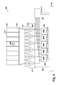
- a detector block 100 is depicted.
- a plurality of detector blocks 100 can be configured in arrangement in a ring around the patient bore.
- the SiPM-based detector block 100 includes a plurality of SiPMs 102 , scintillator crystals 112 , light guides 114 , a front end circuit 113 , group readouts 108 , and a block readout 115 .
- the front end (FE) circuit 113 includes a plurality of buffer amplifiers 106 , respectively coupled to the plurality of SiPMs 102 which can function as a current buffer.
- Each buffer amplifier 106 provides both an output signal 107 to the block readout circuit 115 and output signal 103 to the respective group readout units 108 ; each buffer amplifier is connected to one or more group readout units.
- the plurality of SiPMs 102 are arranged in groups to form sub-blocks 104 , where a plurality of buffer amplifiers 106 respectively receive output signals of the plurality of SiPMs 102 .
- each buffer amplifier is coupled to at least one group readout unit 108 in which the signals 103 are summed and then processed by the readout unit including both timing channel (with short shaping time constant) and energy channel (with long shaping time constant) to provide timing (e.g. T 1 , T 2 , T 3 ) and energy (e.g. E 1 , E 2 , E 3 ) information to control and processing logic unit 110 .
- the SiPM group readout configuration matches with the placement of a reflector 118 .
- Each sub-block 104 corresponds to multiple crystals 112 which share optical photons of detected 511 keV annihilation photons in light guide 114 and are optically-isolated from crystals in other sub-blocks with the use of the reflector 118 (e.g., enhanced specular reflector (ESR), which prevents the optical photon crosstalk between sub-blocks.
- ESR enhanced specular reflector
- the gamma ray interaction 105 in the crystal is depicted here.
- the SiPMs 102 within the block share block readout circuit 115 which provide energy (Eb), timing (Tb), and two-dimensional position (e.g., X position and Z position) information to the control & processing logic unit 110 .
- the group readout 108 could process noisy and slow signals generated by the SiPM to offer improved timing performance with a reduction in the number of readout channels.
- the universal readout system specifically the SiPM-based light sharing detector achieves improved timing performance while maintaining high sensitivity by recovering Compton scatter events between sub-blocks.
- the group readout design having the benefits of reduced contribution of electronics noise, dark noise and optical crosstalk from other channels (i.e., sub-blocks), offers improved timing resolution.
- the signals from each SiPM device 102 in the block are also summed together and then processed in block readout circuit 115 to provide timing (Tb) and energy (Eb) signals for further processing in the control and processing logic unit 110 .
- a group (e.g. sub-block) readout unit 108 from FIG. 2 illustrates an adaptive switching.
- group readout 108 the output signal 103 from the SiPM and the buffer is relayed to a summer 312 through an adaptive switch 311 .
- a timing channel 313 and energy channel 314 is then communicated with the processor 110 .
- the output signal 107 from the SiPM and the buffer is summed and/or weighted in the summer and weighting module 315 as desired, and then respectively processed in a timing channel 316 , an energy channel 317 , and a position channel 318 to offer timing, energy, and two-dimensional position information to the processor 110 .
- the position designated may be one-dimensional, two-dimensional, or three-dimensional.
- FIG. 4A illustrates the adaptive group readouts which are operated at a low count rate condition for system 400 .
- the output of the SiPMs 402 e.g., SiPM 1 , SiPM 2 . . . etc.
- each respective buffer 406 e.g., Buffer 1 , Buffer 2 . . . etc.
- the adaptive switch 410 is controlled by control & processing logic unit 420 to select the signals from designated SiPMs (e.g.
- SiPM/Buffer 1 , 2 , and 3 which are summed in the summer 412 , and then processed in both a timing channel 414 and energy channel 413 .
- the respective timing and energy signal (T 1 and E 1 ) are provided to the control and processing logic unit 420 .
- the adaptive switch 415 in group readout II ( 411 ) selects the designated signal from SiPM/Buffer 4 , 5 , and 6 , and then process the summed signal in the timing channel 417 and energy channel 418 to provide timing and energy signal to the control and processing logic unit 420 .
- FIG. 4B illustrates the adaptive group readouts which are operated at a high count rate condition in system 444 .
- the output of the SiPMs 402 e.g., SiPM 1 , SiPM 2 . . . etc.
- each respective buffer 406 e.g., Buffer 1 , Buffer 2 . . . etc.
- current signals 403 to group readout I ( 409 ), current signals 407 to group readout II ( 411 ), and current signals 429 to group readout III ( 421 ).
- group readout I the adaptive switch 410 is controlled by control & processing logic unit 420 such that the adaptive switch 410 of group readout I ( 409 ) selects a fewer number of buffers (e.g. SiPM/Buffer 1 and 2 ).
- group readout II ( 411 ) and the group readout III ( 421 ) collect the signal from SiPM/Buffer 3 and 4 , and SiPM/Buffer 5 and 6 respectively.
- a flowchart illustrates a determination of the timing signal and improvement in the timing resolution (e.g., coincidence resolving time, (CRT)).
- the decision processing system 500 determines at a first step 502 whether or not a single sub-block (group) event has occurred. If yes, then a time stamp estimation 504 is obtained from the timing signal of the specific group readout. If no, then the signals from two of the group readout units are obtained along with the signals obtained from the block readout circuit ( 506 ) for the same event. In one aspect, signals from two group readout units are obtained, though signals from multiple group units, in any order and arrangement may be obtained.
- These signals specifically comprising (i) an energy distribution, (ii) a spatial distance between one or more single or multiple group events (interactions), and (iii) an observed time difference between the events are checked with a look-up table ( 508 ) to determine the number of inputs and values to be used in calculating the weighted mean values of the time stamps ( 512 ).
- the look-up table can be pre-determined, as part of the processing unit. Multiple timing and energy signal pairs (N) from a single coincidence event are sent to the look-up table. The outputs of the look-up table are the selected timing and energy signal pairs to calculate the weighted mean timing stamp.
- the look-up table can include a pre-determined weighting factor and/or a selection strategy of the timing and energy signal pairs.
- time signals T 1 , T 2 from each group readout unit represent an independent measurement of the arrival time of the 511 keV annihilation photon
- a time stamp is calculated ( 512 ) as an average of two group timing signals, weighted by the inverse of each respective variance at respective energy depositions (E 1 and E 2 ).
- a weighted mean of the time stamp T stamp from two group timing signal can be expressed as shown in equation 1:
- T stamp ⁇ 2 2 ⁇ ( E 2 ) * T 1 + ⁇ 1 2 ⁇ ( E 1 ) * T 2 ⁇ 1 2 ⁇ ( E 1 ) + ⁇ 2 2 ⁇ ( E 2 ) ( EQ . ⁇ 1 )
- a SiPM-based detector 200 includes a plurality of SiPMs 202 arranged in a unitary block 204 ; a plurality of buffer amplifiers 206 respectively coupled to the plurality of SiPMs 202 ; and a plurality of group readouts 208 (e.g., 208 a , 208 b , 208 c , 208 d , 208 e ), wherein each buffer amplifier within the input front-end circuit 213 , is coupled to at least one group readout unit 208 in which the signals are summed and then processed by both timing channel, and energy channel to provide timing (e.g.
- a front-end control signal 220 is provided by the control and processing logic unit 210 .
- the group readout architecture may be configured to far greater than the light spreading (i.e., optical photon distribution) to collecting most of the optical photons in single readout group. This group readout provides the desired timing and energy information with reduced contribution of electronic noise, dark noise and optical crosstalk from other SiPMs, and thus offers improved timing resolution.
- the signals from each SiPM 202 in the scintillation block 204 are also summed together in block readout 207 , and then processed to provide timing (Tb), energy (Eb), and position signal (X, Z) for further processing in control and processing logic unit 210 .
- the scintillation photons can be shared by multiple group readout units 208 .
- the methods disclosed in embodiments herein can process noisy (i.e., dark current), and slow signals generated by SiPM devices.
- the universal readout design includes adaptively multiplexing to greatly reduce the number of readout channels while maintaining a desired ratio of single group events and offering improved timing resolution for the SiPM-based detector with light-sharing configuration,
- the configuration may be modified to utilize a complete readout electronic device for each SiPM.
- This design utilizes a plurality of readout channels, and consumes more power. Configurations that can be simplified and complexity minimized drive down cost and provide easier implementation.
- the embodiments thus described utilize an SiPM in both 1 : 1 coupling (without light guide) or a light-sharing detector.
- a computer program application stored in non-volatile memory or computer-readable medium may include code or executable instructions that when executed may instruct and/or cause a controller or processor to perform methods discussed herein such as improving coincidence resolving time (CRT) in PET scanners using group channel and block channel data from a photomultiplier array, as described above.
- non-volatile memory or computer-readable medium e.g., register memory, processor cache, RAM, ROM, hard drive, flash memory, CD ROM, magnetic media, etc.
- CTR coincidence resolving time
- the computer-readable medium may be a non-transitory computer-readable media including all forms and types of memory and all computer-readable media except for a transitory, propagating signal.
- the non-volatile memory or computer-readable medium may be external memory.
Landscapes
- Physics & Mathematics (AREA)
- Health & Medical Sciences (AREA)
- Life Sciences & Earth Sciences (AREA)
- General Physics & Mathematics (AREA)
- High Energy & Nuclear Physics (AREA)
- Molecular Biology (AREA)
- Spectroscopy & Molecular Physics (AREA)
- Measurement Of Radiation (AREA)
- Nuclear Medicine (AREA)
- Electronic Switches (AREA)
Priority Applications (3)
| Application Number | Priority Date | Filing Date | Title |
|---|---|---|---|
| US15/262,477 US9817134B1 (en) | 2016-09-12 | 2016-09-12 | Universal readout for light-sharing detector |
| JP2017164948A JP7126814B2 (ja) | 2016-09-12 | 2017-08-30 | 光共有検出器のためのユニバーサル読み出し |
| CN201710821485.4A CN107817510B (zh) | 2016-09-12 | 2017-09-12 | 用于光共享检测器的通用读出 |
Applications Claiming Priority (1)
| Application Number | Priority Date | Filing Date | Title |
|---|---|---|---|
| US15/262,477 US9817134B1 (en) | 2016-09-12 | 2016-09-12 | Universal readout for light-sharing detector |
Publications (1)
| Publication Number | Publication Date |
|---|---|
| US9817134B1 true US9817134B1 (en) | 2017-11-14 |
Family
ID=60255784
Family Applications (1)
| Application Number | Title | Priority Date | Filing Date |
|---|---|---|---|
| US15/262,477 Active US9817134B1 (en) | 2016-09-12 | 2016-09-12 | Universal readout for light-sharing detector |
Country Status (3)
| Country | Link |
|---|---|
| US (1) | US9817134B1 (zh) |
| JP (1) | JP7126814B2 (zh) |
| CN (1) | CN107817510B (zh) |
Cited By (2)
| Publication number | Priority date | Publication date | Assignee | Title |
|---|---|---|---|---|
| US11026799B2 (en) | 2009-02-25 | 2021-06-08 | Zimmer, Inc. | Ethnic-specific orthopaedic implants and custom cutting jigs |
| US11694423B2 (en) * | 2019-10-18 | 2023-07-04 | Jefferson Science Associates, Llc | Gated truncated readout system |
Families Citing this family (1)
| Publication number | Priority date | Publication date | Assignee | Title |
|---|---|---|---|---|
| CN112998732B (zh) | 2021-02-08 | 2023-07-18 | 上海联影医疗科技股份有限公司 | Pet数据校正方法、装置、计算机设备以及pet图像重建方法 |
Citations (15)
| Publication number | Priority date | Publication date | Assignee | Title |
|---|---|---|---|---|
| US5504334A (en) | 1993-07-12 | 1996-04-02 | General Electric Company | Signal processing in scintillation cameras for nuclear medicine |
| US8063377B2 (en) | 2008-08-15 | 2011-11-22 | Koninklijke Philips Electronics N.V. | Crystal identification for high resolution nuclear imaging |
| US20120068077A1 (en) * | 2009-05-28 | 2012-03-22 | Koninklijke Philips Electronics N.V. | Method to improve the time resolution of digital silicon photomultipliers |
| US8294110B2 (en) | 2011-03-11 | 2012-10-23 | Kabushiki Kaisha Toshiba | Method for improved correction of SiPM non-linearity in multiplexed radiation detectors |
| US20140061482A1 (en) * | 2012-09-06 | 2014-03-06 | General Electric Company | Enhanced response of solid state photomultiplier to scintillator light by use of wavelength shifters |
| US20140183339A1 (en) * | 2012-12-28 | 2014-07-03 | General Electric Company | Solid State Photomultiplier With Improved Pulse Shape Readout |
| US20140224963A1 (en) * | 2013-02-12 | 2014-08-14 | General Electric Company | Low impedance interface circuit to maximize bandwidth and provide bias control |
| US8849002B2 (en) | 2010-07-07 | 2014-09-30 | The Board Of Trustees Of The Leland Stanford Junior University | Noise robust decoder for multiplexing readout channels on an imaging sensor array |
| US20150001403A1 (en) * | 2013-06-28 | 2015-01-01 | General Electric Company | Methods and systems for signal communication in gamma ray detectors |
| US20150108328A1 (en) * | 2013-10-23 | 2015-04-23 | General Electric Company | System and method for compensating dark current |
| WO2015081134A2 (en) | 2013-11-26 | 2015-06-04 | Flir Detection, Inc. | SiPM-BASED RADIATION DETECTION SYSTEMS AND METHODS |
| US9151847B2 (en) | 2012-05-08 | 2015-10-06 | The Board Of Trustess Of The Leland Stanford Junior University | Optical coupling technique for contiguous monolithic scintillation crystal detectors |
| US9304211B2 (en) | 2013-01-18 | 2016-04-05 | University Of Manitoba | Scintillation detector with active light guide |
| US20160170045A1 (en) * | 2014-12-15 | 2016-06-16 | General Electric Company | Systems and methods for positron emission tomography signal isolation |
| US20160191829A1 (en) * | 2014-12-24 | 2016-06-30 | General Electric Company | Systems and methods for mimimizing silicon photomultiplier signal propagation delay dispersion and improve timing |
Family Cites Families (19)
| Publication number | Priority date | Publication date | Assignee | Title |
|---|---|---|---|---|
| US3517194A (en) * | 1968-10-24 | 1970-06-23 | Atomic Energy Commission | Position-sensitive radiation detector |
| JPS62203076A (ja) * | 1986-02-28 | 1987-09-07 | Shimadzu Corp | Pmtゲイン調節方法 |
| JP3046617B2 (ja) * | 1990-09-26 | 2000-05-29 | 株式会社日立メディコ | シンチレーシヨンカメラ |
| WO2005047955A1 (en) * | 2003-11-12 | 2005-05-26 | Micronic Laser Systems Ab | Method and device for correcting slm stamp image imperfections |
| US8395127B1 (en) * | 2005-04-22 | 2013-03-12 | Koninklijke Philips Electronics N.V. | Digital silicon photomultiplier for TOF PET |
| US7414246B2 (en) * | 2006-01-03 | 2008-08-19 | Koninklijke Philips Electronics N.V. | Achieving accurate time-of-flight calibrations with a stationary coincidence point source |
| US7800439B2 (en) * | 2006-10-27 | 2010-09-21 | Ut-Battelle, Llc | High speed preamplifier circuit, detection electronics, and radiation detection systems therefrom |
| GB2451678A (en) * | 2007-08-10 | 2009-02-11 | Sensl Technologies Ltd | Silicon photomultiplier circuitry for minimal onset and recovery times |
| JP5701616B2 (ja) * | 2008-03-13 | 2015-04-15 | コーニンクレッカ フィリップス エヌ ヴェ | 画像診断装置、画像診断方法及び信号処理回路の電力消費を減少させる方法 |
| JP4880077B1 (ja) * | 2011-02-16 | 2012-02-22 | 株式会社リガク | X線検出信号処理装置および方法 |
| CN102727257B (zh) * | 2011-03-31 | 2016-08-03 | 通用电气公司 | 穿刺针可视化方法和装置 |
| US9140804B2 (en) * | 2012-03-30 | 2015-09-22 | General Electric Company | Methods and systems for determining timing recovery information in a positron emission tomography (PET) system |
| WO2013157448A1 (ja) * | 2012-04-20 | 2013-10-24 | ソニー株式会社 | 半導体光検出装置および放射線検出装置 |
| WO2013168111A2 (en) * | 2012-05-08 | 2013-11-14 | Spectrum Dynamics Llc | Nuclear medicine tomography systems, detectors and methods |
| US9176240B2 (en) | 2012-07-18 | 2015-11-03 | Kabushiki Kaisha Toshiba | Apparatus and method for channel count reduction in solid-state-based positron emission tomography |
| WO2014135465A1 (en) | 2013-03-08 | 2014-09-12 | Koninklijke Philips N.V. | Timestamping detected radiation quanta |
| US9442201B2 (en) * | 2013-09-12 | 2016-09-13 | Siemens Medical Solutions Usa, Inc. | CMOS SPAD array with mixed timing pick-off for time-of-flight positron emission tomography |
| CN105022082B (zh) * | 2015-07-29 | 2018-01-19 | 中派科技(深圳)有限责任公司 | 光子测量前端电路 |
| CN105759301B (zh) * | 2016-04-07 | 2019-04-30 | 中国科学院高能物理研究所 | 基于SiPM的核医学成像平板探测器 |
-
2016
- 2016-09-12 US US15/262,477 patent/US9817134B1/en active Active
-
2017
- 2017-08-30 JP JP2017164948A patent/JP7126814B2/ja active Active
- 2017-09-12 CN CN201710821485.4A patent/CN107817510B/zh active Active
Patent Citations (15)
| Publication number | Priority date | Publication date | Assignee | Title |
|---|---|---|---|---|
| US5504334A (en) | 1993-07-12 | 1996-04-02 | General Electric Company | Signal processing in scintillation cameras for nuclear medicine |
| US8063377B2 (en) | 2008-08-15 | 2011-11-22 | Koninklijke Philips Electronics N.V. | Crystal identification for high resolution nuclear imaging |
| US20120068077A1 (en) * | 2009-05-28 | 2012-03-22 | Koninklijke Philips Electronics N.V. | Method to improve the time resolution of digital silicon photomultipliers |
| US8849002B2 (en) | 2010-07-07 | 2014-09-30 | The Board Of Trustees Of The Leland Stanford Junior University | Noise robust decoder for multiplexing readout channels on an imaging sensor array |
| US8294110B2 (en) | 2011-03-11 | 2012-10-23 | Kabushiki Kaisha Toshiba | Method for improved correction of SiPM non-linearity in multiplexed radiation detectors |
| US9151847B2 (en) | 2012-05-08 | 2015-10-06 | The Board Of Trustess Of The Leland Stanford Junior University | Optical coupling technique for contiguous monolithic scintillation crystal detectors |
| US20140061482A1 (en) * | 2012-09-06 | 2014-03-06 | General Electric Company | Enhanced response of solid state photomultiplier to scintillator light by use of wavelength shifters |
| US20140183339A1 (en) * | 2012-12-28 | 2014-07-03 | General Electric Company | Solid State Photomultiplier With Improved Pulse Shape Readout |
| US9304211B2 (en) | 2013-01-18 | 2016-04-05 | University Of Manitoba | Scintillation detector with active light guide |
| US20140224963A1 (en) * | 2013-02-12 | 2014-08-14 | General Electric Company | Low impedance interface circuit to maximize bandwidth and provide bias control |
| US20150001403A1 (en) * | 2013-06-28 | 2015-01-01 | General Electric Company | Methods and systems for signal communication in gamma ray detectors |
| US20150108328A1 (en) * | 2013-10-23 | 2015-04-23 | General Electric Company | System and method for compensating dark current |
| WO2015081134A2 (en) | 2013-11-26 | 2015-06-04 | Flir Detection, Inc. | SiPM-BASED RADIATION DETECTION SYSTEMS AND METHODS |
| US20160170045A1 (en) * | 2014-12-15 | 2016-06-16 | General Electric Company | Systems and methods for positron emission tomography signal isolation |
| US20160191829A1 (en) * | 2014-12-24 | 2016-06-30 | General Electric Company | Systems and methods for mimimizing silicon photomultiplier signal propagation delay dispersion and improve timing |
Non-Patent Citations (4)
| Title |
|---|
| Kang et al., "PET Detector Configuration with Thick Light Guide and GAPD Array Having Large-Area Microcells", pp. 1-5, http://miil.stanford.edu/publications/files/155-PUB.pdf. |
| Kang et al., "PET Detector Configuration with Thick Light Guide and GAPD Array Having Large-Area Microcells", pp. 1-5, http://miil.stanford.edu/publications/files/155—PUB.pdf. |
| Qi et al., "Performance comparison of two compact multiplexed readouts with SensL's SPMArray4 for high-resolution Detector module", Nuclear Science Symposium and Medical Imaging Conference (NSS/MIC), 2012 IEEE, pp. 455-457, Oct. 27, 2012-Nov. 3, 2012. |
| Xiao-Hui et al., "Design and development of compact readout electronics with silicon photomultiplier array for a compact imaging detector", Chinese Physics C, vol. 36, Issue 10, pp. 973-978, Oct. 2012. |
Cited By (3)
| Publication number | Priority date | Publication date | Assignee | Title |
|---|---|---|---|---|
| US11026799B2 (en) | 2009-02-25 | 2021-06-08 | Zimmer, Inc. | Ethnic-specific orthopaedic implants and custom cutting jigs |
| US11806242B2 (en) | 2009-02-25 | 2023-11-07 | Zimmer, Inc. | Ethnic-specific orthopaedic implants and custom cutting jigs |
| US11694423B2 (en) * | 2019-10-18 | 2023-07-04 | Jefferson Science Associates, Llc | Gated truncated readout system |
Also Published As
| Publication number | Publication date |
|---|---|
| JP7126814B2 (ja) | 2022-08-29 |
| CN107817510B (zh) | 2023-05-12 |
| JP2018044952A (ja) | 2018-03-22 |
| CN107817510A (zh) | 2018-03-20 |
Similar Documents
| Publication | Publication Date | Title |
|---|---|---|
| US9945965B2 (en) | Universal readout for silicon photomultiplier based detectors | |
| JP6556821B2 (ja) | ガンマ線検出器モジュール及び核医学診断装置 | |
| US9029789B2 (en) | Method for detecting radiation, device thereof, and positron emission tomography scanner | |
| JP5641930B2 (ja) | 画像診断システム、タイムスタンプ計算方法、この方法を実行するプロセッサ、この方法をプログラミングしたコンピュータ読取媒体 | |
| US8791514B2 (en) | Providing variable cell density and sizes in a radiation detector | |
| US9029786B2 (en) | Nuclear medicine imaging apparatus, and nuclear medicine imaging method | |
| Lewellen | The challenge of detector designs for PET | |
| US8395125B1 (en) | Silicon photomultiplier trigger network | |
| US20090179154A1 (en) | Nuclear medicine diagnosis equipment | |
| US9182506B2 (en) | Methods and systems for signal communication in gamma ray detectors | |
| Braem et al. | Feasibility of a novel design of high resolution parallax-free Compton enhanced PET scanner dedicated to brain research | |
| JP4670704B2 (ja) | エネルギー較正方法,エネルギー関心領域の設定方法、放射線検出装置及び核医学診断装置 | |
| US9817134B1 (en) | Universal readout for light-sharing detector | |
| EP2461183B1 (en) | Positron emission tomography detector module, radiation detector, positron emission tomography scanner system, method of processing signals, and method of manufacturing radiation detector module | |
| Herbert et al. | The silicon photomultiplier for application to high-resolution positron emission tomography | |
| US20120212355A1 (en) | Encoding for Nuclear Medical Imaging Block Detectors | |
| CN113376681B (zh) | 基于晶体侧面耦合SiPM的PET探测器及其读出方法 | |
| US20100084559A1 (en) | Use of crystal location in nuclear imaging apparatus to minimize timing degradation in a photodetector array | |
| US7253415B2 (en) | Method and apparatus for vetoing random coincidences in positron emission tomographs | |
| Shibuya et al. | Timing resolution improvement using DOI information in a four-layer scintillation detector for TOF-PET | |
| Del Guerra et al. | Advances in position-sensitive photodetectors for PET applications | |
| Li et al. | A high resolution, monolithic crystal, PET/MRI detector with DOI positioning capability | |
| KR102409778B1 (ko) | 방사선의 검출을 이용한 검사 장치 | |
| Salçin et al. | Design considerations for the next-generation MAPMT-based monolithic scintillation camera | |
| Meng et al. | Investigation of the intrinsic spatial resolution of an intensified EMCCD scintillation camera |
Legal Events
| Date | Code | Title | Description |
|---|---|---|---|
| AS | Assignment |
Owner name: GENERAL ELECTRIC COMPANY, NEW YORK Free format text: ASSIGNMENT OF ASSIGNORS INTEREST;ASSIGNORS:FU, GENG;HEUKENSFELDT JANSEN, FLORIBERTUS PM;QIAN, HUA;AND OTHERS;SIGNING DATES FROM 20160907 TO 20160912;REEL/FRAME:039702/0493 |
|
| STCF | Information on status: patent grant |
Free format text: PATENTED CASE |
|
| MAFP | Maintenance fee payment |
Free format text: PAYMENT OF MAINTENANCE FEE, 4TH YEAR, LARGE ENTITY (ORIGINAL EVENT CODE: M1551); ENTITY STATUS OF PATENT OWNER: LARGE ENTITY Year of fee payment: 4 |