US9804628B2 - Reference voltage generator - Google Patents
Reference voltage generator Download PDFInfo
- Publication number
- US9804628B2 US9804628B2 US14/521,669 US201414521669A US9804628B2 US 9804628 B2 US9804628 B2 US 9804628B2 US 201414521669 A US201414521669 A US 201414521669A US 9804628 B2 US9804628 B2 US 9804628B2
- Authority
- US
- United States
- Prior art keywords
- nmos transistor
- reference voltage
- voltage generator
- resistor
- diode
- Prior art date
- Legal status (The legal status is an assumption and is not a legal conclusion. Google has not performed a legal analysis and makes no representation as to the accuracy of the status listed.)
- Expired - Fee Related, expires
Links
Images


Classifications
-
- G—PHYSICS
- G05—CONTROLLING; REGULATING
- G05F—SYSTEMS FOR REGULATING ELECTRIC OR MAGNETIC VARIABLES
- G05F3/00—Non-retroactive systems for regulating electric variables by using an uncontrolled element, or an uncontrolled combination of elements, such element or such combination having self-regulating properties
- G05F3/02—Regulating voltage or current
- G05F3/08—Regulating voltage or current wherein the variable is DC
- G05F3/10—Regulating voltage or current wherein the variable is DC using uncontrolled devices with non-linear characteristics
- G05F3/16—Regulating voltage or current wherein the variable is DC using uncontrolled devices with non-linear characteristics being semiconductor devices
- G05F3/20—Regulating voltage or current wherein the variable is DC using uncontrolled devices with non-linear characteristics being semiconductor devices using diode- transistor combinations
- G05F3/24—Regulating voltage or current wherein the variable is DC using uncontrolled devices with non-linear characteristics being semiconductor devices using diode- transistor combinations wherein the transistors are of the field-effect type only
- G05F3/242—Regulating voltage or current wherein the variable is DC using uncontrolled devices with non-linear characteristics being semiconductor devices using diode- transistor combinations wherein the transistors are of the field-effect type only with compensation for device parameters, e.g. channel width modulation, threshold voltage, processing, or external variations, e.g. temperature, loading, supply voltage
Definitions
- the present invention relates to a reference voltage generator for generating a reference voltage within a semiconductor integrated circuit.
- a power management IC represented by a voltage detector or a voltage regulator
- a reference voltage generator can generate a reference voltage with high precision, that is, temperature characteristics of the reference voltage become flatter.
- FIG. 4 is a circuit diagram of the reference voltage generator in the related art as shown in Japanese Published Patent Application JP 56-108258.
- a depletion NMOS transistor (hereinafter referred to as a D type NMOS transistor) 1 which is connected so as to function as a current source causes a constant current to flow into a diode-connected enhancement NMOS transistor (hereinafter referred to as an E type NMOS transistor) 2 .
- E type NMOS transistor diode-connected enhancement NMOS transistor
- the present invention has been made in view of the demand described above, and it is therefore an object of the present invention to provide a reference voltage generator having flatter temperature characteristics.
- the periphery of a depletion NMOS transistor and an enhancement NMOS transistor which construct a reference voltage generator is surrounded by a resistor.
- the reference voltage generator has a circuit configuration including a diode which can detect temperature and a constant current source.
- the constant current source is trimmed with high precision for a preset temperature. In this way, a constant diode output signal can be obtained under a given temperature environment.
- a voltage with which the constant diode output signal is applied to the resistor is adjusted. In this way, the reference voltage generator operates under a constant temperature environment, and hence shows flatter temperature characteristics.
- the reference voltage generator operates under the given temperature environment, and hence the reference voltage which has been difficult to flatten due to the change in temperature can be flattened.
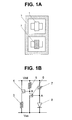
- FIG. 1A is a schematic top plan view illustrating features of a reference voltage generator according to an embodiment of the present invention.
- FIG. 1B is a schematic circuit diagram illustrating the features of the reference voltage generator according to the embodiment of the present invention.
- FIG. 2 is a schematic characteristic graph showing the features of the reference voltage generator according to the embodiment of the present invention.
- FIG. 3 is a schematic characteristic graph showing a reference voltage generator in the related art.
- FIG. 4 is a schematic circuit diagram illustrating the reference voltage generator in the related art.
- FIG. 1A An embodiment of the present invention is now described with reference to the attached drawings. Firstly, a reference voltage generator according to an embodiment of the present invention is described below with reference to a schematic top plan view of FIG. 1A and a schematic circuit diagram of FIG. 1B .
- the reference voltage generator includes a depletion NMOS transistor (hereinafter referred to as a D type NMOS transistor) 1 and an enhancement NMOS transistor (hereinafter referred to as an E type NMOS transistor) 2 .
- the arrangement of the D type NMOS transistor 1 and the E type NMOS transistor 2 is identical to that in the case of the reference voltage generator shown in FIG. 4 in the related art in terms of a circuit configuration.
- the reference voltage generator includes a resistor 3 so as to surround the periphery of the D type NMOS transistor land the E type NMOS transistor 2 .
- the resistor 3 for example, can be formed of a polycrystalline silicon film.
- a resistance value of the resistor 3 can be freely set by selecting a size, a thickness, and a concentration of impurities to be diffused of the polycrystalline silicon film.
- the reference voltage generator according to the embodiment of the present invention further includes a PMOS transistor 4 which is connected in series to the resistor 3 described above, an NMOS transistor 6 which is connected in parallel to the PMOS transistor 4 and in series to another resistor 5 , and a diode 8 which is connected in parallel to the NMOS transistor 6 and in series to a constant current source 7 which can be trimmed with high precision.
- the constant current source 7 of each of the individual ICs can be trimmed for a preset temperature, and hence a bit which is subordinate to a trimming fuse has resolution enough to enable a value of the constant current to be sufficiently set with high precision.
- the preset temperature for example, is 40° C.
- the constant current source 7 is trimmed with high precision for the preset temperature described above, and hence a constant voltage can be applied to a point A of FIG. 1B on the anode side of the diode 8 under a preset temperature environment.
- An output voltage from the diode 8 is applied as a gate voltage of the NMOS transistor 6 having a threshold voltage larger than the output voltage.
- the environment temperature is lower than the preset temperature, in order to compensate for reduction of a current caused to flow through the diode 8 , the voltage developed at the point A is increased, and the NMOS transistor 6 is turned ON to become a conduction state. As a result, a current is caused to flow through the resistor 5 .
- a voltage developed at a point B of FIG. 1B approaches a lower power source voltage Vss.
- the PMOS transistor 4 is also turned ON to become a conduction state. Therefore, the current is caused to flow through the resistor 3 to generate the heat therefrom. If the above-mentioned state of the reference voltage generator is referred to as an ON state, then, when the environment temperature is higher than the preset temperature, both the NMOS transistor 6 and the PMOS transistor 4 become an OFF state by the reverse operation. As a result, no current is caused to flow through the resistor 3 in the circuit of the reference voltage generator.
- the ambient temperature of the D type NMOS transistor 1 and the E type NMOS transistor 2 which serve to generate the reference voltage, is controlled by the heat generating circuit for generating the heat in the resistor 3 described above when the ambient temperature is lower than the preset temperature. In this way, after a lapse of given time, the change in temperature can be kept approximately in the predetermined range.
- the reference voltage generator according to the embodiment of the present invention is capable of obtaining an approximately constant output voltage even when the time has lapsed.
Landscapes
- Engineering & Computer Science (AREA)
- Microelectronics & Electronic Packaging (AREA)
- Physics & Mathematics (AREA)
- Nonlinear Science (AREA)
- Electromagnetism (AREA)
- General Physics & Mathematics (AREA)
- Radar, Positioning & Navigation (AREA)
- Automation & Control Theory (AREA)
- Control Of Electrical Variables (AREA)
- Semiconductor Integrated Circuits (AREA)
- Metal-Oxide And Bipolar Metal-Oxide Semiconductor Integrated Circuits (AREA)
- Power Engineering (AREA)
Abstract
Description
Claims (1)
Applications Claiming Priority (2)
| Application Number | Priority Date | Filing Date | Title |
|---|---|---|---|
| JP2013-222586 | 2013-10-25 | ||
| JP2013222586A JP6205238B2 (en) | 2013-10-25 | 2013-10-25 | Reference voltage generator |
Publications (2)
| Publication Number | Publication Date |
|---|---|
| US20150115912A1 US20150115912A1 (en) | 2015-04-30 |
| US9804628B2 true US9804628B2 (en) | 2017-10-31 |
Family
ID=52994674
Family Applications (1)
| Application Number | Title | Priority Date | Filing Date |
|---|---|---|---|
| US14/521,669 Expired - Fee Related US9804628B2 (en) | 2013-10-25 | 2014-10-23 | Reference voltage generator |
Country Status (5)
| Country | Link |
|---|---|
| US (1) | US9804628B2 (en) |
| JP (1) | JP6205238B2 (en) |
| KR (1) | KR20150048053A (en) |
| CN (1) | CN104571244B (en) |
| TW (1) | TWI654825B (en) |
Cited By (1)
| Publication number | Priority date | Publication date | Assignee | Title |
|---|---|---|---|---|
| US20240045454A1 (en) * | 2022-08-05 | 2024-02-08 | Navitas Semiconductor Limited | Gallium nitride reference voltage generation circuit |
Families Citing this family (2)
| Publication number | Priority date | Publication date | Assignee | Title |
|---|---|---|---|---|
| JP2020035307A (en) * | 2018-08-31 | 2020-03-05 | エイブリック株式会社 | Constant current circuit |
| JP2020177393A (en) * | 2019-04-17 | 2020-10-29 | エイブリック株式会社 | Constant current circuit and semiconductor device |
Citations (7)
| Publication number | Priority date | Publication date | Assignee | Title |
|---|---|---|---|---|
| US3781648A (en) * | 1973-01-10 | 1973-12-25 | Fairchild Camera Instr Co | Temperature compensated voltage regulator having beta compensating means |
| US4008406A (en) * | 1974-11-07 | 1977-02-15 | Hitachi, Ltd. | Electronic circuit using field effect transistor with compensation means |
| US4205263A (en) * | 1976-08-03 | 1980-05-27 | Tokyo Shibaura Electric Co., Ltd. | Temperature compensated constant current MOS field effective transistor circuit |
| US5253201A (en) * | 1991-07-25 | 1993-10-12 | Kabushiki Kaisha Toshiba | Writing control circuit employed in non-volatile semiconductor memory device |
| US6087821A (en) * | 1998-10-07 | 2000-07-11 | Ricoh Company, Ltd. | Reference-voltage generating circuit |
| US20030197552A1 (en) * | 2002-03-20 | 2003-10-23 | Hirofumi Watanabe | Reference voltage source circuit operating with low voltage |
| US20110102071A1 (en) * | 2009-11-02 | 2011-05-05 | Delphi Technologies, Inc. | Curvature-compensated band-gap voltage reference circuit |
Family Cites Families (12)
| Publication number | Priority date | Publication date | Assignee | Title |
|---|---|---|---|---|
| JPS56108258A (en) * | 1980-02-01 | 1981-08-27 | Seiko Instr & Electronics Ltd | Semiconductor device |
| JPS61161749A (en) * | 1985-01-11 | 1986-07-22 | Yokogawa Electric Corp | Semiconductor device |
| JP3940485B2 (en) | 1997-02-27 | 2007-07-04 | 東芝マイクロエレクトロニクス株式会社 | Reference voltage generation circuit |
| JP2000025258A (en) * | 1998-07-13 | 2000-01-25 | Seiko Instruments Inc | Thermal head and driving ic for heating resistors |
| JP2002140124A (en) * | 2000-10-30 | 2002-05-17 | Seiko Epson Corp | Reference voltage circuit |
| JP2002368107A (en) * | 2001-06-07 | 2002-12-20 | Ricoh Co Ltd | Reference voltage generation circuit and power supply device using the same |
| US20060043957A1 (en) * | 2004-08-30 | 2006-03-02 | Carvalho Carlos M | Resistance trimming in bandgap reference voltage sources |
| US7342407B2 (en) * | 2006-01-31 | 2008-03-11 | Advantest Corporation | Temperature compensation circuit and testing apparatus |
| US8044677B2 (en) * | 2008-12-19 | 2011-10-25 | Stmicroelectronics S.R.L. | Electrical system, voltage reference generation circuit, and calibration method of the circuit |
| JP4955042B2 (en) * | 2009-05-18 | 2012-06-20 | 日本電波工業株式会社 | Constant temperature crystal oscillator |
| CN201548864U (en) * | 2009-11-19 | 2010-08-11 | 贵州大学 | High precision and low drift integrated voltage reference source circuit |
| JP5957852B2 (en) * | 2011-11-10 | 2016-07-27 | 株式会社ソシオネクスト | Inspection apparatus and inspection method for semiconductor device |
-
2013
- 2013-10-25 JP JP2013222586A patent/JP6205238B2/en not_active Expired - Fee Related
-
2014
- 2014-10-14 TW TW103135529A patent/TWI654825B/en not_active IP Right Cessation
- 2014-10-22 KR KR1020140143218A patent/KR20150048053A/en not_active Ceased
- 2014-10-23 US US14/521,669 patent/US9804628B2/en not_active Expired - Fee Related
- 2014-10-24 CN CN201410573195.9A patent/CN104571244B/en not_active Expired - Fee Related
Patent Citations (7)
| Publication number | Priority date | Publication date | Assignee | Title |
|---|---|---|---|---|
| US3781648A (en) * | 1973-01-10 | 1973-12-25 | Fairchild Camera Instr Co | Temperature compensated voltage regulator having beta compensating means |
| US4008406A (en) * | 1974-11-07 | 1977-02-15 | Hitachi, Ltd. | Electronic circuit using field effect transistor with compensation means |
| US4205263A (en) * | 1976-08-03 | 1980-05-27 | Tokyo Shibaura Electric Co., Ltd. | Temperature compensated constant current MOS field effective transistor circuit |
| US5253201A (en) * | 1991-07-25 | 1993-10-12 | Kabushiki Kaisha Toshiba | Writing control circuit employed in non-volatile semiconductor memory device |
| US6087821A (en) * | 1998-10-07 | 2000-07-11 | Ricoh Company, Ltd. | Reference-voltage generating circuit |
| US20030197552A1 (en) * | 2002-03-20 | 2003-10-23 | Hirofumi Watanabe | Reference voltage source circuit operating with low voltage |
| US20110102071A1 (en) * | 2009-11-02 | 2011-05-05 | Delphi Technologies, Inc. | Curvature-compensated band-gap voltage reference circuit |
Non-Patent Citations (1)
| Title |
|---|
| Patent Abstracts of Japan, Publication No. 56-108258, Publication Date Aug. 27, 1981. |
Cited By (1)
| Publication number | Priority date | Publication date | Assignee | Title |
|---|---|---|---|---|
| US20240045454A1 (en) * | 2022-08-05 | 2024-02-08 | Navitas Semiconductor Limited | Gallium nitride reference voltage generation circuit |
Also Published As
| Publication number | Publication date |
|---|---|
| TWI654825B (en) | 2019-03-21 |
| JP6205238B2 (en) | 2017-09-27 |
| US20150115912A1 (en) | 2015-04-30 |
| CN104571244B (en) | 2018-01-19 |
| KR20150048053A (en) | 2015-05-06 |
| TW201531002A (en) | 2015-08-01 |
| CN104571244A (en) | 2015-04-29 |
| JP2015084175A (en) | 2015-04-30 |
Similar Documents
| Publication | Publication Date | Title |
|---|---|---|
| CN113157033B (en) | Constant current circuit and semiconductor device | |
| US8922188B2 (en) | Low pass filter circuit and voltage regulator | |
| US7973525B2 (en) | Constant current circuit | |
| US9552009B2 (en) | Reference voltage generator having diode-connected depletion MOS transistors with same temperature coefficient | |
| US8026756B2 (en) | Bandgap voltage reference circuit | |
| US7965129B1 (en) | Temperature compensated current reference circuit | |
| US9246479B2 (en) | Low-offset bandgap circuit and offset-cancelling circuit therein | |
| TW201116968A (en) | Pico-power reference voltage generator | |
| JP6289083B2 (en) | Reference voltage generation circuit | |
| JP2013003699A (en) | Semiconductor integrated circuit for regulator | |
| US20120249187A1 (en) | Current source circuit | |
| US9804628B2 (en) | Reference voltage generator | |
| WO2016013983A1 (en) | A method for providing a voltage reference at a present operating temperature in a circuit | |
| US10274981B2 (en) | Voltage dropping apparatus, voltage switching apparatus, and internal voltage supply apparatus using the same | |
| US10180694B2 (en) | Adaptive body bias for voltage regulator | |
| US20200336141A1 (en) | Supply voltage supervisor | |
| JP5121587B2 (en) | Reference voltage circuit | |
| US7834609B2 (en) | Semiconductor device with compensation current | |
| JP6013851B2 (en) | Reference voltage generator | |
| JP2005122753A (en) | Temperature detection circuit, heating protection circuit, and various electronic devices incorporating these circuits | |
| US10082813B1 (en) | Constant voltage circuit | |
| CN113866486A (en) | Ultra-low power supply voltage detection circuit | |
| US20200177174A1 (en) | Overheat protection circuit and semiconductor device including the same | |
| JP2018022280A (en) | Voltage Regulator | |
| WO2021038230A1 (en) | Apparatus for producing an electrical signal that is indicative of a temperature |
Legal Events
| Date | Code | Title | Description |
|---|---|---|---|
| AS | Assignment |
Owner name: SEIKO INSTRUMENTS INC., JAPAN Free format text: ASSIGNMENT OF ASSIGNORS INTEREST;ASSIGNORS:HASHITANI, MASAYUKI;HIROSE, YOSHITSUGU;REEL/FRAME:034017/0335 Effective date: 20141023 |
|
| AS | Assignment |
Owner name: SII SEMICONDUCTOR CORPORATION, JAPAN Free format text: ASSIGNMENT OF ASSIGNORS INTEREST;ASSIGNOR:SEIKO INSTRUMENTS INC.;REEL/FRAME:038058/0892 Effective date: 20160105 |
|
| STCF | Information on status: patent grant |
Free format text: PATENTED CASE |
|
| AS | Assignment |
Owner name: ABLIC INC., JAPAN Free format text: CHANGE OF NAME;ASSIGNOR:SII SEMICONDUCTOR CORPORATION;REEL/FRAME:045567/0927 Effective date: 20180105 |
|
| MAFP | Maintenance fee payment |
Free format text: PAYMENT OF MAINTENANCE FEE, 4TH YEAR, LARGE ENTITY (ORIGINAL EVENT CODE: M1551); ENTITY STATUS OF PATENT OWNER: LARGE ENTITY Year of fee payment: 4 |
|
| AS | Assignment |
Owner name: ABLIC INC., JAPAN Free format text: CHANGE OF ADDRESS;ASSIGNOR:ABLIC INC.;REEL/FRAME:064021/0575 Effective date: 20230424 |
|
| FEPP | Fee payment procedure |
Free format text: MAINTENANCE FEE REMINDER MAILED (ORIGINAL EVENT CODE: REM.); ENTITY STATUS OF PATENT OWNER: LARGE ENTITY |
|
| LAPS | Lapse for failure to pay maintenance fees |
Free format text: PATENT EXPIRED FOR FAILURE TO PAY MAINTENANCE FEES (ORIGINAL EVENT CODE: EXP.); ENTITY STATUS OF PATENT OWNER: LARGE ENTITY |
|
| STCH | Information on status: patent discontinuation |
Free format text: PATENT EXPIRED DUE TO NONPAYMENT OF MAINTENANCE FEES UNDER 37 CFR 1.362 |
|
| FP | Lapsed due to failure to pay maintenance fee |
Effective date: 20251031 |