US20120249187A1 - Current source circuit - Google Patents
Current source circuit Download PDFInfo
- Publication number
- US20120249187A1 US20120249187A1 US13/428,288 US201213428288A US2012249187A1 US 20120249187 A1 US20120249187 A1 US 20120249187A1 US 201213428288 A US201213428288 A US 201213428288A US 2012249187 A1 US2012249187 A1 US 2012249187A1
- Authority
- US
- United States
- Prior art keywords
- node
- current
- circuit
- pmos transistor
- gate
- Prior art date
- Legal status (The legal status is an assumption and is not a legal conclusion. Google has not performed a legal analysis and makes no representation as to the accuracy of the status listed.)
- Abandoned
Links
- 230000002194 synthesizing effect Effects 0.000 claims abstract description 12
- 230000000694 effects Effects 0.000 description 8
- 102100037224 Noncompact myelin-associated protein Human genes 0.000 description 7
- 101710184695 Noncompact myelin-associated protein Proteins 0.000 description 7
- 239000003990 capacitor Substances 0.000 description 5
- 230000015654 memory Effects 0.000 description 5
- 239000004065 semiconductor Substances 0.000 description 5
- 230000000052 comparative effect Effects 0.000 description 4
- 230000004048 modification Effects 0.000 description 4
- 238000012986 modification Methods 0.000 description 4
- 238000000034 method Methods 0.000 description 3
- 230000008569 process Effects 0.000 description 3
- 230000007423 decrease Effects 0.000 description 2
- 230000001419 dependent effect Effects 0.000 description 2
- 230000005611 electricity Effects 0.000 description 2
- 230000006870 function Effects 0.000 description 2
- 230000008901 benefit Effects 0.000 description 1
- 230000008859 change Effects 0.000 description 1
- 230000006866 deterioration Effects 0.000 description 1
- 238000007599 discharging Methods 0.000 description 1
- 238000006467 substitution reaction Methods 0.000 description 1
- 238000009966 trimming Methods 0.000 description 1
Images


Classifications
-
- G—PHYSICS
- G05—CONTROLLING; REGULATING
- G05F—SYSTEMS FOR REGULATING ELECTRIC OR MAGNETIC VARIABLES
- G05F3/00—Non-retroactive systems for regulating electric variables by using an uncontrolled element, or an uncontrolled combination of elements, such element or such combination having self-regulating properties
- G05F3/02—Regulating voltage or current
- G05F3/08—Regulating voltage or current wherein the variable is DC
- G05F3/10—Regulating voltage or current wherein the variable is DC using uncontrolled devices with non-linear characteristics
- G05F3/16—Regulating voltage or current wherein the variable is DC using uncontrolled devices with non-linear characteristics being semiconductor devices
- G05F3/20—Regulating voltage or current wherein the variable is DC using uncontrolled devices with non-linear characteristics being semiconductor devices using diode- transistor combinations
- G05F3/24—Regulating voltage or current wherein the variable is DC using uncontrolled devices with non-linear characteristics being semiconductor devices using diode- transistor combinations wherein the transistors are of the field-effect type only
- G05F3/242—Regulating voltage or current wherein the variable is DC using uncontrolled devices with non-linear characteristics being semiconductor devices using diode- transistor combinations wherein the transistors are of the field-effect type only with compensation for device parameters, e.g. channel width modulation, threshold voltage, processing, or external variations, e.g. temperature, loading, supply voltage
Definitions
- Embodiments described herein relate generally to a current source circuit.
- NAND flash memories are widely used as these memories.
- a semiconductor integrated circuit including the above-mentioned NAND flash memory improves the circuit performance by using a constant current source and constant voltage source. Therefore, it is required to implement an accurate constant current source and accurate constant voltage source.
- the constant current source is used to, e.g., accurately generate a given delay time, and accurately generate various voltages.
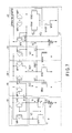
- FIG. 1 is a view showing a configuration example of a current source circuit according to the first embodiment
- FIG. 2A is a graph showing the relationship between the constant current value and temperature characteristic in a current source circuit according to a comparative example
- FIG. 2B is a graph showing the relationship between the constant current value and temperature characteristic in the current source circuit according to the first embodiment
- FIG. 3 is a view showing an application example of the current source circuit according to the first embodiment
- FIG. 4 is a view showing a configuration example of a current source circuit according to the second embodiment
- FIG. 5 is a view showing an application example of the current source circuit according to the second embodiment
- FIG. 6 is a view showing a configuration example of a current source circuit according to the third embodiment.
- FIG. 7 is a view showing a configuration example of a current source circuit according to the fourth embodiment.
- FIG. 8 is view showing a delay circuit using the constant current source according to each embodiment.
- FIG. 9 is a view showing a charging circuit using the constant current source according to each embodiment.
- a current source circuit comprises a first current generating circuit, second current generating circuit, and current synthesizing circuit.
- the first current generating circuit includes a first current mirror circuit including PMOS transistors, and a second current mirror circuit including NMOS transistors, and generates a first current having a positive temperature characteristic.
- the second current generating circuit includes a feedback circuit configured to receive a first voltage depending on a threshold voltage of the NMOS transistors and having a negative temperature characteristic, and output a second voltage equal to the first voltage, and generates a second current having the negative temperature characteristic based on the second voltage.
- the current synthesizing circuit generates a constant current having an arbitrary temperature characteristic by adding the first and second currents.
- FIGS. 1 , 2 A, 2 B, and 3 A semiconductor integrated circuit according to the first embodiment will be explained below with reference to FIGS. 1 , 2 A, 2 B, and 3 .
- FIG. 1 is a view showing a configuration example of a current source circuit according to the first embodiment.
- the current source circuit includes a first current generating circuit 10 , second current generating circuit 20 , and current synthesizing circuit 30 .
- the first current generating circuit 10 includes a first current mirror circuit 11 , second current mirror circuit 12 , and variable resistor R 1 .
- the first current mirror circuit 11 includes PMOS transistors MP 1 and MP 2 . More specifically, the sources of the PMOS transistors MP 1 and MP 2 are connected to the power supply. The gates of the PMOS transistors MP 1 and MP 2 are connected together to a node BIASP. The drain of the PMOS transistor MP 1 is connected to a node VC (to be described later). The drain of the PMOS transistor MP 2 is connected to the node BIASP to form a diode connection. That is, the potential difference between one end (the source) and the other end (the drain) of the current path of the PMOS transistor MP 2 is equal to that between one end (the source) of the current path and the gate of the PMOS transistor MP 2 . Accordingly, the PMOS transistor MP 2 operates as a pentode.
- the second current mirror circuit 12 includes NMOS transistors MN 1 and MN 2 forming a current mirror. More specifically, the source of the NMOS transistor MN 1 is connected to the ground potential. The source of the NMOS transistor MN 2 is connected to one end of the variable resistor R 1 via a node VB. The other end of the variable resistor R 1 is connected to the ground potential. The gates of the NMOS transistors MN 1 and MN 2 are connected together to the node VC. The drain of the NMOS transistor MN 2 is connected to the node BIASP. The drain of the NMOS transistor MN 1 is connected to the node VC to form a diode connection.
- the potential difference between one end (the source) and the other end (the drain) of the current path of the NMOS transistor MN 1 is equal to that between one end (the source) of the current path and the gate of the NMOS transistor MN 1 . Therefore, the NMOS transistor MN 1 operates as a pentode. Also, the number of NMOS transistors MN 2 is N times that of NMOS transistors MN 1 , and the NMOS transistors MN 2 are connected in parallel. In other words, the size of the NMOS transistor MN 2 is N times that of the NMOS transistor MN 1 .
- the current paths of the PMOS transistor MP 1 and NMOS transistor MN 1 are connected in series, and the current paths of the PMOS transistor MP 2 and NMOS transistor MN 2 and the variable resistor R 1 are connected in series, between the power supply and ground potential.
- the PMOS transistors MP 1 and MP 2 are turned on, and a current flows through the node VC. Consequently, the node VC is boosted from the power supply via the PMOS transistors MP 1 and MP 2 .
- the NMOS transistors MN 1 and MN 2 are turned on. Thus, a current flows through each transistor and each node.
- the PMOS transistors MP 1 and MP 2 form a current mirror
- the NMOS transistors MN 1 and MN 2 form a current mirror. Therefore, a current Ip equal to that of the PMOS transistor MP 2 and NMOS transistor MN 2 flows through the PMOS transistor MP 1 and NMOS transistor MN 1 .
- the current Ip is generated as follows.
- a potential difference is produced between the gate-to-source potential of the NMOS transistor MN 1 and that of the NMOS transistor MN 2 .
- This potential difference generates a voltage VB of the node VB.
- the current Ip is generated by applying the voltage VB to the variable resistor R 1 .
- the value of the current Ip is controlled by the variable resistor R 1 and the number (size) of NMOS transistors MN 2 .
- the variable resistor R 1 is adjusted for each chip in accordance the process variations (the power supply potential and the resistance and threshold value of each transistor). This makes it possible to generate, for each chip, the current Ip as a constant current independent of the process variations.
- the current IP generated as described above is represented by
- Ip 2 ⁇ ⁇ ⁇ R 2 ⁇ ( N N - 1 ) 2 ( 1 )
- the first current generating circuit 10 generates the current Ip having the positive temperature characteristic.
- the second current generating circuit 20 includes a differential amplifier 21 , PMOS transistor MP 5 , and variable resistor R 2 .
- the differential amplifier 21 includes PMOS transistors MP 6 and MP 7 forming a current mirror, and NMOS transistors MN 4 , MN 5 , and MN 6 .
- the sources of the PMOS transistors MP 6 and MP 7 are connected to the power supply.
- the gates of the PMOS transistors MP 6 and MP 7 are connected together to the same node.
- the drain of the PMOS transistor MP 6 is connected to a node BIASC as the output node of the differential amplifier 21 .
- the drain of the PMOS transistor MP 7 is connected together with its gate to the same node to form a diode connection. That is, the potential difference between one end (the source) and the other end (the drain) of the current path of the PMOS transistor MP 7 is equal to that between one end (the source) of the current path and the gate of the PMOS transistor MP 7 . Therefore, the PMOS transistor MP 7 operates as a pentode.
- the sources of the NMOS transistors MN 4 and MN 5 are connected together to the same node as that of the drain of the NMOS transistor MN 6 , and the source of the NMOS transistor MN 6 is grounded.
- the gate of the NMOS transistor MN 4 is connected to the node VC of the first current generating circuit 10 , which is the first input node of the differential amplifier 21 .
- the gate of the NMOS transistor MN 5 is connected to a node VC 2 as the second input node of the differential amplifier 21 .
- the drain of the NMOS transistor MN 4 is connected to the node BIASC.
- the drain of the NMOS transistor MN 5 is connected together with the drain and gate of the PMOS transistor MP 7 to the same node.
- the source of the PMOS transistor MP 5 is connected to the power supply.
- the gate of the PMOS transistor MP 5 is connected to the node BIASC.
- the drain of the PMOS transistor MP 5 is connected to the node VC 2 , and grounded via the variable resistor R 2 .
- the variable resistor R 2 is connected between the node VC 2 and ground potential. That is, the variable resistor R 2 has one end connected to the node VC 2 , and the other end that is grounded.
- the second current generating circuit 20 operates when the voltages of the node VC and a node VIREF (to be described later) exceed threshold voltages.
- the operating current of the differential amplifier 21 is determined by inputting a voltage VIREF of the node VIREF to the gate of the NMOS transistor MN 6 .
- the NMOS transistors MN 4 and MN 6 are turned on. Consequently, the voltage of the node BIASC exceeds the threshold voltage, and the PMOS transistor MP 5 is turned on.
- a current Ic flows through the node VC 2 , the potential rises, and the NMOS transistor MN 5 is turned on when the potential exceeds the threshold voltage.
- the PMOS transistors MP 6 and MP 7 are turned on when the voltages of their gates rise and exceed the threshold voltages.
- the current Ic flows through the PMOS transistor MP 5 and variable resistor R 2 .
- the current Ic is generated as follows.
- the voltage of the node VC of the first current generating circuit 10 is applied to the gate of the NMOS transistor MN 4 .
- the PMOS transistors MP 6 and MP 7 form a current mirror.
- the node BIASC is controlled by making the PMOS transistors MP 6 and PMOS transistors MP 7 equal in size (number), and making the NMOS transistors MN 4 and NMOS transistors MN 5 equal in size (number), thereby generating a voltage VC 2 equal to a voltage VC of the node VC.
- the differential amplifier 21 functions as a feedback circuit that outputs the same voltage as an input voltage. In other words, the differential amplifier 21 functions as an amplifier having a gain of 1.
- the node VC is the diode-connected node of the NMOS transistor MN 1 , and the voltage VC is represented by
- Vth is the threshold voltage of the NMOS transistor MN 1 .
- the threshold voltage Vth has the negative temperature characteristic. Accordingly, the voltage VC of the node VC and the voltage VC 2 of the node VC 2 each have a value having the negative temperature characteristic.
- the current Ic is generated by applying the voltage VC 2 to the variable resistor R 2 .
- the variable resistor R 2 controls the value of the current Ic. This makes it possible to generate, for each chip, the current Ic as a constant current independent of the process variations.
- the current Ic generated as described above is represented by
- Ic 2 x ⁇ ⁇ ⁇ ⁇ ⁇ R 2 ⁇ ( N N - 1 ) + Vth xR ( 3 )
- the threshold voltage Vth has the negative temperature characteristic. Therefore, the value of the current Ic generated by the second current generating circuit 20 has the negative temperature characteristic. Thus, the second current generating circuit 20 generates the current Ic having the negative temperature characteristic.
- the current synthesizing circuit 30 includes PMOS transistors MP 3 and MP 4 , and an NMOS transistor MN 3 .
- the source of the PMOS transistor MP 3 is connected to the power supply.
- the gate of the PMOS transistor MP 3 is connected together with the gates of the PMOS transistors MP 1 and MP 2 to the node BIASP. That is, the PMOS transistor MP 3 forms a current mirror together with the PMOS transistor MP 2 .
- the source of the PMOS transistor MP 4 is connected to the power supply potential.
- the gate of the PMOS transistor MP 4 is connected together with the gate of the PMOS transistor MP 5 to the node BIASC.
- the drains of the PMOS transistors MP 3 and MP 4 are connected together to the node VIREF as an output node.
- the source of the NMOS transistor MN 3 is connected to the ground potential.
- the drain of the NMOS transistor MN 3 is connected together with its gate to the node VIREF to form a diode connection.
- the current synthesizing circuit 30 operates when the voltage of the node BIASP exceeds the threshold voltage. That is, the PMOS transistor MP 3 is turned on when the voltage of the node BIASP exceeds the threshold voltage. Since a current flows through the node VIREF, the potential rises, and the NMOS transistor MN 3 is turned on when the potential exceeds the threshold voltage. In this state, the second current generating circuit 20 operates when the voltage of the node VIREF exceeds the threshold voltage as described above, so the voltage of the node BIASC exceeds the threshold voltage. This turns on the PMOS transistor MP 4 . Thus, a current flows through each transistor and each node.
- the PMOS transistor MP 3 forms a current mirror together with the PMOS transistor MP 2 . Accordingly, the current Ip equal to that of the PMOS transistor MP 2 flows through the PMOS transistor MP 3 .
- the number of PMOS transistors MP 3 (the number of transistors connected in parallel) is equal to those of PMOS transistors MP 1 and MP 2 in FIG. 1 , but the former need not be equal to the latter and is suitably changed in accordance with the addition ratio to the current Ic (to be described later).
- the gate of the PMOS transistor MP 4 is connected together with the gate of the PMOS transistor MP 5 to the node BIASC. Therefore, the current Ic equal to that of the PMOS transistor MP 5 flows through the PMOS transistor MP 4 .
- the current Ic flowing through the PMOS transistor MP 4 will be explained in detail below.
- the PMOS transistors MP 6 and MP 7 form a current mirror. Accordingly, equal currents flow through the PMOS transistor MP 6 and NMOS transistor MN 4 , and through the PMOS transistor MP 7 and NMOS transistor MN 5 . If the PMOS transistors MP 6 and MP 7 have the same size, therefore, the PMOS transistors MP 6 and MP 7 have the same gate-to-source potential and the same drain-to-source potential in an equilibrium state.
- the PMOS transistors MP 4 , MP 5 , MP 6 , and MP 7 form a pseudo current mirror. Since the circuit is configured as described above, the current Ic generated in the PMOS transistor MP 5 can be supplied (mirrored) to the PMOS transistor MP 4 .
- the number of PMOS transistors MP 4 is equal to that of PMOS transistors MP 5 in FIG. 1 , but the former need not be equal to the latter and is suitably changed in accordance with the addition ratio to the current Ip.
- a current IREF generated by adding the currents Ip and Ic can be supplied to the NMOS transistor MN 3 , and the voltage VIREF can be output.
- the current IREF thus generated is represented by
- Ip + Ic 1 ⁇ ⁇ ⁇ R 2 ⁇ ⁇ 2 x ⁇ ( N N - 1 ) + 2 ( N N - 1 ) 2 ⁇ + Vth xR ( 4 )
- the current IREF includes a term having the positive temperature characteristic and a term having the negative temperature characteristic.
- the addition ratio of the current Ip to the current Ic can be changed by adjusting the ratio of the number (size) of PMOS transistors MP 3 to that of PMOS transistors MP 4 (by adjusting the mirror current ratio).
- the current source circuit includes the first current generating circuit 10 for generating the constant current Ip having the positive temperature characteristic, the second current generating circuit 20 for generating the constant current Ic having the negative temperature characteristic, and the current synthesizing circuit 30 for generating the constant current IREF having a zero temperature characteristic (independent of the temperature) by adding the two constant currents described above. Accordingly, the following effects can be obtained.
- FIG. 2A is a graph showing the relationship between the constant current value and temperature characteristic in a current source circuit according to a comparative example.
- FIG. 2B is a graph showing the relationship between the constant current value and temperature characteristic in the current source circuit according to the first embodiment. Referring to FIGS. 2A and 2B , the abscissa indicates the temperature, the ordinate indicates the constant current value, and a plurality of plots indicate the changes (absolute value shifts) in current value caused by trimming.
- the constant current of the current source circuit according to the comparative example has the positive temperature characteristic by which a current increases as the temperature rises. Therefore, the dependence on the temperature remains even when the constant current value is trimmed for each chip. This deteriorates the circuit characteristics of an analog circuit using the constant current because the dependence on the temperature appears in the characteristics.
- the current source circuit according to this comparative example is a circuit having, e.g., the same configuration as that of the first current generating circuit 10 shown in FIG. 1 .
- the constant current IREF of the current source circuit according to the first embodiment is constant regardless of the temperature. This is so because the positive and negative temperature characteristics are canceled by adding the current Ip having the positive temperature characteristic and the current Ic having the negative temperature characteristic by appropriately adjusting these currents.
- the first embodiment can improve the temperature characteristics and performances of various analog circuits by using the current source circuit that generates the constant current IREF independent of the temperature in these analog circuits.
- the number of NMOS transistors MN 2 and the variable resistors R 1 and R 2 are set such that the temperature characteristic of the current IREF becomes zero.
- the present embodiment is not limited to this, and the current IREF can be adjusted to either the positive or negative temperature characteristic by changing these values.
- the current source circuit according to the first embodiment makes the temperature characteristic variable by connecting the differential amplifier 21 including a current mirror circuit, and connecting the PMOS transistor MP 5 and variable resistor R 2 , to the conventional current source circuit (including only the first current generating circuit 10 ). That is, since the increase in number of elements is minimum, the increase in circuit area can also be minimized.
- FIG. 3 is a view showing an application example of the current source circuit according to the first embodiment. Note that in this application example, an explanation of the same features as those of the aforementioned first embodiment will be omitted, and different features will be explained.
- this application example differs from the above-mentioned first embodiment in that PMOS transistors MP 1 ′ to MP 5 ′ are respectively connected in series with the drains of the PMOS transistors MP 1 to MP 5 .
- the sources of the PMOS transistors MP 1 ′ to MP 5 ′ are respectively connected to the drains of the PMOS transistors MP 1 to MP 5 .
- the gates of the PMOS transistors MP 1 ′ to MP 3 ′ are connected together to the same node as that of the drain of the NMOS transistor MN 2 .
- the gates of the PMOS transistors MP 4 ′ and MP 5 ′ are connected together to the node VC 2 .
- the drain of the PMOS transistor MP 1 ′ is connected to the node VC.
- the drains of the PMOS transistors MP 3 ′ and MP 4 ′ are connected together to the node VIREF.
- the drain of the PMOS transistor MP 2 ′ is connected to the same node as that of its gate, thereby forming a diode connection. That is, the potential difference between one end (the source) and the other end (the drain) of the current path of the PMOS transistor MP 2 ′ is equal to that between one end (the source) of the current path and the gate of the PMOS transistor MP 2 ′. Accordingly, the PMOS transistor MP 2 ′ operates as a pentode. Likewise, the drain of the PMOS transistor MP 5 ′ is connected to the same node (the node VC 2 ) as that of its gate, thereby forming a diode connection.
- the potential difference between one end (the source) and the other end (the drain) of the current path of the PMOS transistor MP 5 ′ is equal to that between one end (the source) of the current path and the gate of the PMOS transistor MP 5 ′. Accordingly, the PMOS transistor MP 5 ′ operates as a pentode.
- the PMOS transistors MP 1 ′ to MP 3 ′ are turned on when the potential of the common node connected to their gates exceeds the threshold voltage.
- the PMOS transistors MP 4 ′ and MP 5 ′ are turned on when the voltage of the node VC 2 exceeds the threshold voltage.
- the NMOS transistor MN 5 is turned on.
- the second embodiment is a modification of the first embodiment, in which the operating current of a differential amplifier 21 is determined by inputting a signal different from that of the first embodiment to the gate of an NMOS transistor MN 6 forming the differential amplifier 21 .
- the second embodiment an explanation of the same features as those of the aforementioned first embodiment will be omitted, and different features will be explained.
- FIG. 4 is a view showing a configuration example of a current source circuit according to the second embodiment.
- the second embodiment differs from the above-mentioned first embodiment in that a second current generating circuit 20 includes a PMOS transistor MP 8 and NMOS transistor NM 7 .
- the PMOS transistor MP 8 has a source connected to the power supply, and a gate connected to a node BIASC.
- the drain of the PMOS transistor MP 8 is connected to a node VA.
- the drain of the NMOS transistor MN 7 is connected together with its gate to the node VA, thereby forming a diode connection.
- the source of the NMOS transistor MN 7 is grounded. That is, the current paths of the PMOS transistor MP 8 and NMOS transistor MN 7 are connected in series between the power supply potential and ground potential.
- the gate of an NMOS transistor MN 6 is connected together with the gate (and drain) of the NMOS transistor MN 7 to the node VA.
- the differential amplifier 21 operates when the voltage of a node VC exceeds a threshold voltage. That is, when the voltage of the node VC exceeds the threshold voltage, a current flows through each transistor and each node of the differential amplifier 21 . In this state, the operating current of the differential amplifier 21 is determined by applying a voltage VA of the node VA to the gate of the NMOS transistor MN 6 . Also, the node VA is biased by turning on the PMOS transistor MP 8 having a gate connected to the node BIASC.
- the second embodiment described above can achieve the same effects as those of the first embodiment.
- FIG. 5 is a view showing an application example of the current source circuit according to the second embodiment. Note that in this application example, an explanation of the same features as those of the aforesaid second embodiment will be omitted, and different features will be explained.
- this application example differs from the above-described second embodiment in that PMOS transistors MP 1 ′ to MP 5 ′ and MP 8 ′ are respectively connected in series with the drains of PMOS transistors MP 1 to MP 5 and the PMOS transistor MP 8 .
- the sources of the PMOS transistors MP 1 ′ to MP 5 ′ and MP 8 ′ are respectively connected to the drains of the PMOS transistors MP 1 to MP 5 and MP 8 .
- the gates of the PMOS transistors MP 1 ′ to MP 3 ′ are connected together to the same node as that of the drain of an NMOS transistor MN 2 .
- the gates of the PMOS transistors MP 4 ′, MP 5 ′, and MP 8 ′ are connected together to the node VA.
- the drain of the PMOS transistor MP 1 ′ is connected to the node VC.
- the drains of the PMOS transistors MP 3 ′ and MP 4 ′ are connected together to a node VIREF.
- the drain of the PMOS transistor MP 5 ′ is connected to a node VC 2 .
- the drain of the PMOS transistor MP 2 ′ is connected to the same node as that of its gate, thereby forming a diode connection.
- the drain of the PMOS transistor MP 8 ′ is connected to the same node (the node VA) as that of its gate, thereby forming a diode connection. That is, the potential difference between one end (the source) and the other end (the drain) of the current path of the PMOS transistor MP 8 ′ is equal to that between one end (the source) of the current path and the gate of the PMOS transistor MP 8 ′. Accordingly, the PMOS transistor MP 8 ′ operates as a pentode.
- the PMOS transistors MP 1 ′ to MP 3 ′ are turned on when the voltage of the common node connected to their gates exceeds a threshold voltage.
- the PMOS transistors MP 4 ′, MP 5 ′, and MP 8 ′ are turned on when the voltage of the node VA exceeds a threshold voltage.
- the NMOS transistors MN 6 and MN 7 are turned on.
- the third embodiment is a modification of the first embodiment, in which the operating current of a differential amplifier 21 is determined by inputting a signal different from that of the first embodiment to the gate of an NMOS transistor MN 6 forming the differential amplifier 21 . Note that in the third embodiment, an explanation of the same features as those of the above-mentioned first embodiment will be omitted, and different features will be explained.
- FIG. 6 is a view showing a configuration example of a current source circuit according to the third embodiment.
- the third embodiment differs from the aforementioned first embodiment in that a second current generating circuit 20 includes a PMOS transistor MP 9 and NMOS transistor MN 8 .
- the PMOS transistor MP 9 has a source connected to the power supply, and a gate connected to a node BIASP.
- the drain of the PMOS transistor MP 9 is connected to a node VA.
- the drain of the NMOS transistor MN 8 is connected together with its gate to the node VA, thereby forming a diode connection.
- the source of the NMOS transistor MN 8 is grounded. That is, the current paths of the PMOS transistor MP 9 and NMOS transistor MN 8 are connected in series between the power supply potential and ground potential.
- the gate of an NMOS transistor MN 6 is connected together with the gate (and drain) of the NMOS transistor MN 8 to the node VA.
- the differential amplifier 21 operates when the voltage of a node VC exceeds a threshold voltage. That is, when the voltage of the node VC exceeds the threshold voltage, a current flows through each transistor and each node of the differential amplifier 21 . In this state, the operating current of the differential amplifier 21 is determined by inputting a voltage VA of the node VA to the gate of the NMOS transistor MN 6 . Also, the node VA is biased by turning on a PMOS transistor MP 9 having a gate connected to the node BIASP.
- the third embodiment described above can achieve the same effects as those of the first embodiment.
- the fourth embodiment is a modification of the first embodiment, in which the circuit includes a third current generating circuit 40 and fourth current generating circuit 50 . Note that in the fourth embodiment, an explanation of the same features as those of the aforesaid first embodiment will be omitted, and different features will be explained.
- FIG. 7 is a view showing a configuration example of a current source circuit according to the fourth embodiment.
- the fourth embodiment differs from the above-described first embodiment in that the circuit includes the third current generating circuit 40 for generating a constant current Ip 2 , and the fourth current generating circuit 50 for generating a constant current Ic 2 .
- the third current generating circuit 40 includes a PMOS transistor MP 10 and NMOS transistor MN 9 .
- the PMOS transistor MP 10 has a source connected to the power supply, and a gate connected together with the gates of PMOS transistors MP 1 and MP 2 to a node BIASP. That is, the PMOS transistor MP 10 forms a current mirror together with the PMOS transistor MP 2 .
- the drain of the PMOS transistor MP 10 is connected to a node VIP as an output node.
- the drain of the NMOS transistor MN 9 is connected together with its gate to the node VIP, thereby forming a diode connection.
- the source of the NMOS transistor MN 9 is connected to the ground potential. That is, the current paths of the PMOS transistor MP 10 and NMOS transistor MN 9 are connected in series between the power supply potential and ground potential.
- the third current generating circuit 40 operates when the voltage of the node BIASP exceeds a threshold voltage. That is, the PMOS transistor MP 10 is turned on when the voltage of the node BIASP exceeds the threshold voltage. Consequently, the node VIP is biased, and the NMOS transistor MN 9 is turned on. Thus, a current flows through each transistor and each node.
- the PMOS transistor MP 10 forms the current mirror together with the PMOS transistor MP 2 . Therefore, the constant current Ip 2 equal to a current Ip of the PMOS transistor MP 2 flows through the PMOS transistor MP 10 , and a voltage VIP is output. That is, the current Ip 2 has the same positive temperature characteristic as that of the current Ip.
- the value of the current Ip 2 can be adjusted by adjusting the number (size) of NMOS transistors MN 9 .
- the fourth current generating circuit 50 includes a PMOS transistor MP 11 and NMOS transistor MN 10 . More specifically, the PMOS transistor MP 11 has a source connected to the power supply, and a gate connected together with the gate of a PMOS transistor MP 5 to a node BIASC. The drain of the PMOS transistor MP 11 is connected to a node VIC as an output node. The drain of the NMOS transistor MN 10 is connected together with its gate to the node VIC, thereby forming a diode connection. The source of the NMOS transistor MN 10 is grounded. That is, the current paths of the PMOS transistor MP 11 and NMOS transistor MN 10 are connected in series between the power supply potential and ground potential.
- the fourth current generating circuit 50 operates when the voltage of the node BIASC exceeds a threshold voltage. That is, the PMOS transistor MP 11 is turned on when the voltage of the node BIASC exceeds the threshold voltage. Consequently, the node VIC is biased, and the NMOS transistor MN 10 is turned on. Thus, a current flows through each transistor and each node.
- the gate of the PMOS transistor MP 11 is connected together with the gate of the PMOS transistor MP 5 to the node BIASC. Therefore, the constant current Ic 2 equal to a current Ic of the PMOS transistor MP 5 flows through the PMOS transistor MP 11 , and a voltage VIC is output. That is, the current Ic 2 has the same negative temperature characteristic as that of the current Ic.
- the value of the current Ic 2 can be adjusted by adjusting the number (size) of NMOS transistors MN 10 .
- the fourth embodiment described above can achieve the same effects as those of the first embodiment.
- the fourth embodiment includes, as independent circuits, the third current generating circuit 40 for generating the current Ip 2 having the positive temperature characteristic, and the fourth current generating circuit 50 for generating the current Ic 2 having the negative temperature characteristic.
- This makes it possible to simultaneously use the current Ip 2 as a constant current having the positive temperature characteristic and the current Ic 2 as a constant current having the negative temperature characteristic, in addition to a current IREF having a zero temperature characteristic. That is, these constant currents can selectively be used in accordance with the temperature characteristics of individual parts of an analog circuit using the current source circuit.
- a PMOS transistor MP 10 ′ (not shown) is installed in the third current generating circuit 40 .
- the PMOS transistor MP 10 ′ has a source connected to the power supply potential, a gate connected to the node BIASC, and a drain connected to the drain of the PMOS transistor MP 10 . That is, since the gate is connected to the node BIASC, a current having the negative temperature characteristic flows through the PMOS transistor MP 10 ′.
- the temperature characteristic of the constant current Ip 2 can suitably be set by adjusting the ratio of the number of PMOS transistors MP 10 to that of PMOS transistors MP 10 ′.
- FIG. 8A is a view showing the arrangement of a delay circuit using the constant current source according to each embodiment described above.
- this delay circuit includes a PMOS transistor MP 81 , NMOS transistors MN 81 and MN 82 , a capacitor C 1 , and an inverter INV.
- VIREF from the current source circuit is applied to the gate of the NMOS transistor MN 82 . That is, the NMOS transistor 82 forms a current mirror circuit together with the NMOS transistor MN 3 .
- the PMOS transistor MP 81 When an input signal IN is “L”, the PMOS transistor MP 81 is turned on, and a node n 1 is charged (boosted) to the power supply potential. The capacitor C 1 stores the charged (boosted) electricity. In this state, the NMOS transistor 81 is kept OFF.
- an output signal can be generated by delaying the leading edge of the input signal by a predetermined time by discharging the electricity charged in the node n 1 by the constant current of the NMOS transistor MN 82 .
- the delay time of the delay circuit similarly depends on the temperature. For example, as shown in FIG. 8B , the delay time of the delay circuit at a low temperature is longer than that at a high temperature.
- FIG. 9 is a view showing the arrangement of a charging circuit using the constant current source according to each embodiment described above.
- this charging circuit includes PMOS transistors MP 91 , MP 92 , MP 93 , and MP 94 , NMOS transistors MN 91 and MN 92 , and a capacitor C 1 .
- VIREF from the current source circuit is applied to the gate of the NMOS transistor MN 91 . That is, the NMOS transistor MN 91 forms a current mirror together with the NMOS transistor MN 3 .
- This charging circuit charges a specific node (e.g., a bit line BL of a NAND flash memory).
- a signal ENB controls the charging circuit.
- the signal ENB is “L”
- the PMOS transistor MP 94 is turned on, and the NMOS transistor MN 92 and PMOS transistor MP 93 are turned off. Since a node P is charged, therefore, the PMOS transistor MP 92 is also turned off, and the circuit operation stops.
- the PMOS transistor MP 94 When the signal ENB changes to “H”, the PMOS transistor MP 94 is turned off, and the NMOS transistor MN 92 and PMOS transistor MP 93 are turned on. Consequently, a constant current flows through the PMOS transistor MP 91 , and the capacitor C 1 is charged by this constant current by supplying the constant current from the PMOS transistor MP 91 to the PMOS transistor MP 92 by a current mirror. Since the capacitor is charged with the constant current, the charging time can be made constant, and the peak current can also be suppressed.
- the charging speed and peak current value also depend on the temperature.
- constant current source can also be used in analog circuits such as a clock generator and differential amplifier.
- the clock generator can generate a clock having a predetermined period by using a constant current and constant voltage. However, the clock period becomes temperature-dependent if the constant current and constant voltage used are temperature-dependent.
- the differential amplifier when the differential amplifier is operated by applying a constant voltage as the output from the constant current source as a bias current, it is possible to always hold the operating current of the amplifier constant and hold the operating speed and operation margin constant. Even in this case, however, if the input constant voltage fluctuates due to the temperature, the current flowing through the amplifier also has a temperature characteristic. This poses problems such as deterioration (a decrease) in operating speed of the amplifier during a low-temperature operation.
Landscapes
- Engineering & Computer Science (AREA)
- Microelectronics & Electronic Packaging (AREA)
- Physics & Mathematics (AREA)
- Nonlinear Science (AREA)
- Electromagnetism (AREA)
- General Physics & Mathematics (AREA)
- Radar, Positioning & Navigation (AREA)
- Automation & Control Theory (AREA)
- Control Of Electrical Variables (AREA)
- Amplifiers (AREA)
Abstract
According to one embodiment, a current source circuit comprises a first circuit, a second circuit, and a current synthesizing circuit. The first circuit generates a first current having a positive temperature characteristic. The second circuit includes a feedback circuit configured to receive a first voltage having a negative temperature characteristic, and output a second voltage equal to the first voltage, and generates a second current having the negative temperature characteristic based on the second voltage. The current synthesizing circuit generates a constant current having an arbitrary temperature characteristic by adding the first and second currents.
Description
- This application is based upon and claims the benefit of priority from prior Japanese Patent Application No. 2011-080382, filed Mar. 31, 2011, the entire contents of which are incorporated herein by reference.
- Embodiments described herein relate generally to a current source circuit.
- Recently, as mobile apparatuses such as cell phones spread, memories for use in these apparatuses are required to have a high operating speed and low current consumption. NAND flash memories are widely used as these memories.
- A semiconductor integrated circuit including the above-mentioned NAND flash memory improves the circuit performance by using a constant current source and constant voltage source. Therefore, it is required to implement an accurate constant current source and accurate constant voltage source. The constant current source is used to, e.g., accurately generate a given delay time, and accurately generate various voltages.
-
FIG. 1 is a view showing a configuration example of a current source circuit according to the first embodiment; -
FIG. 2A is a graph showing the relationship between the constant current value and temperature characteristic in a current source circuit according to a comparative example; -
FIG. 2B is a graph showing the relationship between the constant current value and temperature characteristic in the current source circuit according to the first embodiment; -
FIG. 3 is a view showing an application example of the current source circuit according to the first embodiment; -
FIG. 4 is a view showing a configuration example of a current source circuit according to the second embodiment; -
FIG. 5 is a view showing an application example of the current source circuit according to the second embodiment; -
FIG. 6 is a view showing a configuration example of a current source circuit according to the third embodiment; -
FIG. 7 is a view showing a configuration example of a current source circuit according to the fourth embodiment; -
FIG. 8 is view showing a delay circuit using the constant current source according to each embodiment; and -
FIG. 9 is a view showing a charging circuit using the constant current source according to each embodiment. - In general, according to one embodiment, a current source circuit comprises a first current generating circuit, second current generating circuit, and current synthesizing circuit. The first current generating circuit includes a first current mirror circuit including PMOS transistors, and a second current mirror circuit including NMOS transistors, and generates a first current having a positive temperature characteristic. The second current generating circuit includes a feedback circuit configured to receive a first voltage depending on a threshold voltage of the NMOS transistors and having a negative temperature characteristic, and output a second voltage equal to the first voltage, and generates a second current having the negative temperature characteristic based on the second voltage. The current synthesizing circuit generates a constant current having an arbitrary temperature characteristic by adding the first and second currents.
- Embodiments will be explained below with reference to the accompanying drawing. In the drawing, the same reference numerals and symbols denote the same parts. Note that the voltages of nodes VC, VC2, VIREF, VIP, VIC, VA, and VB will be explained as they are respectively abbreviated as voltages VC, VC2, VIREF, VIP, VIC, VA, and VB in some cases.
- It will be understood that when an element is referred to as being “electrically connected to” or “connected to” another element, it can be not only directly connected but also connected to the other element or intervening elements may be present.
- A semiconductor integrated circuit according to the first embodiment will be explained below with reference to
FIGS. 1 , 2A, 2B, and 3. -
FIG. 1 is a view showing a configuration example of a current source circuit according to the first embodiment. - As shown in
FIG. 1 , the current source circuit includes a firstcurrent generating circuit 10, secondcurrent generating circuit 20, and current synthesizingcircuit 30. - The first
current generating circuit 10 includes a firstcurrent mirror circuit 11, secondcurrent mirror circuit 12, and variable resistor R1. - The first
current mirror circuit 11 includes PMOS transistors MP1 and MP2. More specifically, the sources of the PMOS transistors MP1 and MP2 are connected to the power supply. The gates of the PMOS transistors MP1 and MP2 are connected together to a node BIASP. The drain of the PMOS transistor MP1 is connected to a node VC (to be described later). The drain of the PMOS transistor MP2 is connected to the node BIASP to form a diode connection. That is, the potential difference between one end (the source) and the other end (the drain) of the current path of the PMOS transistor MP2 is equal to that between one end (the source) of the current path and the gate of the PMOS transistor MP2. Accordingly, the PMOS transistor MP2 operates as a pentode. - The second
current mirror circuit 12 includes NMOS transistors MN1 and MN2 forming a current mirror. More specifically, the source of the NMOS transistor MN1 is connected to the ground potential. The source of the NMOS transistor MN2 is connected to one end of the variable resistor R1 via a node VB. The other end of the variable resistor R1 is connected to the ground potential. The gates of the NMOS transistors MN1 and MN2 are connected together to the node VC. The drain of the NMOS transistor MN2 is connected to the node BIASP. The drain of the NMOS transistor MN1 is connected to the node VC to form a diode connection. That is, the potential difference between one end (the source) and the other end (the drain) of the current path of the NMOS transistor MN1 is equal to that between one end (the source) of the current path and the gate of the NMOS transistor MN1. Therefore, the NMOS transistor MN1 operates as a pentode. Also, the number of NMOS transistors MN2 is N times that of NMOS transistors MN1, and the NMOS transistors MN2 are connected in parallel. In other words, the size of the NMOS transistor MN2 is N times that of the NMOS transistor MN1. - In the first
current generating circuit 10 as described above, the current paths of the PMOS transistor MP1 and NMOS transistor MN1 are connected in series, and the current paths of the PMOS transistor MP2 and NMOS transistor MN2 and the variable resistor R1 are connected in series, between the power supply and ground potential. - When the voltage of the node BIASP exceeds a threshold voltage in the first
current generating circuit 10, the PMOS transistors MP1 and MP2 are turned on, and a current flows through the node VC. Consequently, the node VC is boosted from the power supply via the PMOS transistors MP1 and MP2. When the voltage of the node VC exceeds a threshold voltage, the NMOS transistors MN1 and MN2 are turned on. Thus, a current flows through each transistor and each node. - As described above, the PMOS transistors MP1 and MP2 form a current mirror, and the NMOS transistors MN1 and MN2 form a current mirror. Therefore, a current Ip equal to that of the PMOS transistor MP2 and NMOS transistor MN2 flows through the PMOS transistor MP1 and NMOS transistor MN1. The current Ip is generated as follows.
- Since the number of NMOS transistors MN2 is N times that of NMOS transistor MN1, a potential difference is produced between the gate-to-source potential of the NMOS transistor MN1 and that of the NMOS transistor MN2. This potential difference generates a voltage VB of the node VB. The current Ip is generated by applying the voltage VB to the variable resistor R1. The value of the current Ip is controlled by the variable resistor R1 and the number (size) of NMOS transistors MN2. In addition, the variable resistor R1 is adjusted for each chip in accordance the process variations (the power supply potential and the resistance and threshold value of each transistor). This makes it possible to generate, for each chip, the current Ip as a constant current independent of the process variations. The current IP generated as described above is represented by
-
- where β is the mobility of electric charge. Since β has a negative temperature characteristic (β increases as the temperature decreases), the current Ip has a positive temperature characteristic (the current Ip increases as the temperature rises). Thus, the first
current generating circuit 10 generates the current Ip having the positive temperature characteristic. - The second current generating
circuit 20 includes adifferential amplifier 21, PMOS transistor MP5, and variable resistor R2. - The
differential amplifier 21 includes PMOS transistors MP6 and MP7 forming a current mirror, and NMOS transistors MN4, MN5, and MN6. - More specifically, the sources of the PMOS transistors MP6 and MP7 are connected to the power supply. The gates of the PMOS transistors MP6 and MP7 are connected together to the same node. The drain of the PMOS transistor MP6 is connected to a node BIASC as the output node of the
differential amplifier 21. The drain of the PMOS transistor MP7 is connected together with its gate to the same node to form a diode connection. That is, the potential difference between one end (the source) and the other end (the drain) of the current path of the PMOS transistor MP7 is equal to that between one end (the source) of the current path and the gate of the PMOS transistor MP7. Therefore, the PMOS transistor MP7 operates as a pentode. - The sources of the NMOS transistors MN4 and MN5 are connected together to the same node as that of the drain of the NMOS transistor MN6, and the source of the NMOS transistor MN6 is grounded. The gate of the NMOS transistor MN4 is connected to the node VC of the first
current generating circuit 10, which is the first input node of thedifferential amplifier 21. The gate of the NMOS transistor MN5 is connected to a node VC2 as the second input node of thedifferential amplifier 21. - The drain of the NMOS transistor MN4 is connected to the node BIASC. The drain of the NMOS transistor MN5 is connected together with the drain and gate of the PMOS transistor MP7 to the same node.
- The source of the PMOS transistor MP5 is connected to the power supply. The gate of the PMOS transistor MP5 is connected to the node BIASC. The drain of the PMOS transistor MP5 is connected to the node VC2, and grounded via the variable resistor R2. In other words, the variable resistor R2 is connected between the node VC2 and ground potential. That is, the variable resistor R2 has one end connected to the node VC2, and the other end that is grounded.
- The second current generating
circuit 20 operates when the voltages of the node VC and a node VIREF (to be described later) exceed threshold voltages. In this state, the operating current of thedifferential amplifier 21 is determined by inputting a voltage VIREF of the node VIREF to the gate of the NMOS transistor MN6. When the voltages of the nodes VC and VIREF exceed the threshold voltages, the NMOS transistors MN4 and MN6 are turned on. Consequently, the voltage of the node BIASC exceeds the threshold voltage, and the PMOS transistor MP5 is turned on. Also, when a current Ic flows through the node VC2, the potential rises, and the NMOS transistor MN5 is turned on when the potential exceeds the threshold voltage. Furthermore, the PMOS transistors MP6 and MP7 are turned on when the voltages of their gates rise and exceed the threshold voltages. Thus, a current flows through each transistor and each node. - In this state, the current Ic flows through the PMOS transistor MP5 and variable resistor R2. The current Ic is generated as follows.
- As described above, the voltage of the node VC of the first
current generating circuit 10 is applied to the gate of the NMOS transistor MN4. Also, the PMOS transistors MP6 and MP7 form a current mirror. In this configuration, the node BIASC is controlled by making the PMOS transistors MP6 and PMOS transistors MP7 equal in size (number), and making the NMOS transistors MN4 and NMOS transistors MN5 equal in size (number), thereby generating a voltage VC2 equal to a voltage VC of the node VC. That is, thedifferential amplifier 21 functions as a feedback circuit that outputs the same voltage as an input voltage. In other words, thedifferential amplifier 21 functions as an amplifier having a gain of 1. - The node VC is the diode-connected node of the NMOS transistor MN1, and the voltage VC is represented by
-
- where Vth is the threshold voltage of the NMOS transistor MN1. The threshold voltage Vth has the negative temperature characteristic. Accordingly, the voltage VC of the node VC and the voltage VC2 of the node VC2 each have a value having the negative temperature characteristic.
- The current Ic is generated by applying the voltage VC2 to the variable resistor R2. The variable resistor R2 controls the value of the current Ic. This makes it possible to generate, for each chip, the current Ic as a constant current independent of the process variations. The current Ic generated as described above is represented by
-
- where x is the ratio (R2=xR1) of the variable resistor R1 to the variable resistor R2. As described above, the threshold voltage Vth has the negative temperature characteristic. Therefore, the value of the current Ic generated by the second current generating
circuit 20 has the negative temperature characteristic. Thus, the second current generatingcircuit 20 generates the current Ic having the negative temperature characteristic. - The
current synthesizing circuit 30 includes PMOS transistors MP3 and MP4, and an NMOS transistor MN3. - The source of the PMOS transistor MP3 is connected to the power supply. The gate of the PMOS transistor MP3 is connected together with the gates of the PMOS transistors MP1 and MP2 to the node BIASP. That is, the PMOS transistor MP3 forms a current mirror together with the PMOS transistor MP2. The source of the PMOS transistor MP4 is connected to the power supply potential. The gate of the PMOS transistor MP4 is connected together with the gate of the PMOS transistor MP5 to the node BIASC. The drains of the PMOS transistors MP3 and MP4 are connected together to the node VIREF as an output node. The source of the NMOS transistor MN3 is connected to the ground potential. The drain of the NMOS transistor MN3 is connected together with its gate to the node VIREF to form a diode connection.
- The
current synthesizing circuit 30 operates when the voltage of the node BIASP exceeds the threshold voltage. That is, the PMOS transistor MP3 is turned on when the voltage of the node BIASP exceeds the threshold voltage. Since a current flows through the node VIREF, the potential rises, and the NMOS transistor MN3 is turned on when the potential exceeds the threshold voltage. In this state, the second current generatingcircuit 20 operates when the voltage of the node VIREF exceeds the threshold voltage as described above, so the voltage of the node BIASC exceeds the threshold voltage. This turns on the PMOS transistor MP4. Thus, a current flows through each transistor and each node. - As described previously, the PMOS transistor MP3 forms a current mirror together with the PMOS transistor MP2. Accordingly, the current Ip equal to that of the PMOS transistor MP2 flows through the PMOS transistor MP3. Note that the number of PMOS transistors MP3 (the number of transistors connected in parallel) is equal to those of PMOS transistors MP1 and MP2 in
FIG. 1 , but the former need not be equal to the latter and is suitably changed in accordance with the addition ratio to the current Ic (to be described later). - On the other hand, the gate of the PMOS transistor MP4 is connected together with the gate of the PMOS transistor MP5 to the node BIASC. Therefore, the current Ic equal to that of the PMOS transistor MP5 flows through the PMOS transistor MP4. The current Ic flowing through the PMOS transistor MP4 will be explained in detail below.
- In the
differential amplifier 21, the PMOS transistors MP6 and MP7 form a current mirror. Accordingly, equal currents flow through the PMOS transistor MP6 and NMOS transistor MN4, and through the PMOS transistor MP7 and NMOS transistor MN5. If the PMOS transistors MP6 and MP7 have the same size, therefore, the PMOS transistors MP6 and MP7 have the same gate-to-source potential and the same drain-to-source potential in an equilibrium state. - That is, all of the gate and drain of the PMOS transistor MP6, the gate and drain of the PMOS transistor MP7, the gate of the PMOS transistor MP5, and the gate of the PMOS transistor MP4 have the same voltage. Thus, the PMOS transistors MP4, MP5, MP6, and MP7 form a pseudo current mirror. Since the circuit is configured as described above, the current Ic generated in the PMOS transistor MP5 can be supplied (mirrored) to the PMOS transistor MP4.
- Note that the number of PMOS transistors MP4 is equal to that of PMOS transistors MP5 in
FIG. 1 , but the former need not be equal to the latter and is suitably changed in accordance with the addition ratio to the current Ip. - By connecting the drains of the PMOS transistors MP3 and MP4 together to the drain of the NMOS transistor MN3, a current IREF generated by adding the currents Ip and Ic can be supplied to the NMOS transistor MN3, and the voltage VIREF can be output. The current IREF thus generated is represented by
-
- As represented by equation (4), the current IREF includes a term having the positive temperature characteristic and a term having the negative temperature characteristic. As described above, the addition ratio of the current Ip to the current Ic can be changed by adjusting the ratio of the number (size) of PMOS transistors MP3 to that of PMOS transistors MP4 (by adjusting the mirror current ratio). Also, it is possible to adjust the value of the current Ip by the number of NMOS transistors MN2 (the ratio to the number of NMOS transistors MN1) and the variable resistor R1, and the value of the current Ic by the variable resistor R2. That is, the temperature characteristic of the current IREF can be set to zero (the dependence on the temperature can be eliminated) by properly adjusting the resistance ratio x, the number of NMOS transistors MN2, or the mirror current ratio.
- In the above-mentioned first embodiment, the current source circuit includes the first
current generating circuit 10 for generating the constant current Ip having the positive temperature characteristic, the second current generatingcircuit 20 for generating the constant current Ic having the negative temperature characteristic, and thecurrent synthesizing circuit 30 for generating the constant current IREF having a zero temperature characteristic (independent of the temperature) by adding the two constant currents described above. Accordingly, the following effects can be obtained. -
FIG. 2A is a graph showing the relationship between the constant current value and temperature characteristic in a current source circuit according to a comparative example.FIG. 2B is a graph showing the relationship between the constant current value and temperature characteristic in the current source circuit according to the first embodiment. Referring toFIGS. 2A and 2B , the abscissa indicates the temperature, the ordinate indicates the constant current value, and a plurality of plots indicate the changes (absolute value shifts) in current value caused by trimming. - As shown in
FIG. 2A , the constant current of the current source circuit according to the comparative example has the positive temperature characteristic by which a current increases as the temperature rises. Therefore, the dependence on the temperature remains even when the constant current value is trimmed for each chip. This deteriorates the circuit characteristics of an analog circuit using the constant current because the dependence on the temperature appears in the characteristics. The current source circuit according to this comparative example is a circuit having, e.g., the same configuration as that of the firstcurrent generating circuit 10 shown inFIG. 1 . - By contrast, as shown in
FIG. 2B , the constant current IREF of the current source circuit according to the first embodiment is constant regardless of the temperature. This is so because the positive and negative temperature characteristics are canceled by adding the current Ip having the positive temperature characteristic and the current Ic having the negative temperature characteristic by appropriately adjusting these currents. Thus, the first embodiment can improve the temperature characteristics and performances of various analog circuits by using the current source circuit that generates the constant current IREF independent of the temperature in these analog circuits. - Note that in the example shown in
FIG. 2B , the number of NMOS transistors MN2 and the variable resistors R1 and R2 are set such that the temperature characteristic of the current IREF becomes zero. However, the present embodiment is not limited to this, and the current IREF can be adjusted to either the positive or negative temperature characteristic by changing these values. - It is also possible to freely adjust the temperature characteristic of the current IREF by changing the ratio of the number of PMOS transistors MP2 to that of PMOS transistors MP3, and the ratio of the number of PMOS transistors MP4 to that of PMOS transistors MP5 (the mirror current ratio).
- Furthermore, the current source circuit according to the first embodiment makes the temperature characteristic variable by connecting the
differential amplifier 21 including a current mirror circuit, and connecting the PMOS transistor MP5 and variable resistor R2, to the conventional current source circuit (including only the first current generating circuit 10). That is, since the increase in number of elements is minimum, the increase in circuit area can also be minimized. -
FIG. 3 is a view showing an application example of the current source circuit according to the first embodiment. Note that in this application example, an explanation of the same features as those of the aforementioned first embodiment will be omitted, and different features will be explained. - As shown in
FIG. 3 , this application example differs from the above-mentioned first embodiment in that PMOS transistors MP1′ to MP5′ are respectively connected in series with the drains of the PMOS transistors MP1 to MP5. - More specifically, the sources of the PMOS transistors MP1′ to MP5′ are respectively connected to the drains of the PMOS transistors MP1 to MP5. The gates of the PMOS transistors MP1′ to MP3′ are connected together to the same node as that of the drain of the NMOS transistor MN2. The gates of the PMOS transistors MP4′ and MP5′ are connected together to the node VC2.
- The drain of the PMOS transistor MP1′ is connected to the node VC. The drains of the PMOS transistors MP3′ and MP4′ are connected together to the node VIREF.
- The drain of the PMOS transistor MP2′ is connected to the same node as that of its gate, thereby forming a diode connection. That is, the potential difference between one end (the source) and the other end (the drain) of the current path of the PMOS transistor MP2′ is equal to that between one end (the source) of the current path and the gate of the PMOS transistor MP2′. Accordingly, the PMOS transistor MP2′ operates as a pentode. Likewise, the drain of the PMOS transistor MP5′ is connected to the same node (the node VC2) as that of its gate, thereby forming a diode connection. That is, the potential difference between one end (the source) and the other end (the drain) of the current path of the PMOS transistor MP5′ is equal to that between one end (the source) of the current path and the gate of the PMOS transistor MP5′. Accordingly, the PMOS transistor MP5′ operates as a pentode.
- The PMOS transistors MP1′ to MP3′ are turned on when the potential of the common node connected to their gates exceeds the threshold voltage. The PMOS transistors MP4′ and MP5′ are turned on when the voltage of the node VC2 exceeds the threshold voltage. At the same time, the NMOS transistor MN5 is turned on.
- By respectively connecting the PMOS transistors MP1′ to MP5′ in series with the PMOS transistors MP1 to MP5, it is possible to suppress the dependence of the whole circuit on the power supply voltage, and improve the reliability of the circuit operation.
- A semiconductor integrated circuit according to the second embodiment will be explained below with reference to
FIGS. 4 and 5 . The second embodiment is a modification of the first embodiment, in which the operating current of adifferential amplifier 21 is determined by inputting a signal different from that of the first embodiment to the gate of an NMOS transistor MN6 forming thedifferential amplifier 21. Note that in the second embodiment, an explanation of the same features as those of the aforementioned first embodiment will be omitted, and different features will be explained. -
FIG. 4 is a view showing a configuration example of a current source circuit according to the second embodiment. - As shown in
FIG. 4 , the second embodiment differs from the above-mentioned first embodiment in that a second current generatingcircuit 20 includes a PMOS transistor MP8 and NMOS transistor NM7. - More specifically, the PMOS transistor MP8 has a source connected to the power supply, and a gate connected to a node BIASC. The drain of the PMOS transistor MP8 is connected to a node VA. The drain of the NMOS transistor MN7 is connected together with its gate to the node VA, thereby forming a diode connection. The source of the NMOS transistor MN7 is grounded. That is, the current paths of the PMOS transistor MP8 and NMOS transistor MN7 are connected in series between the power supply potential and ground potential. The gate of an NMOS transistor MN6 is connected together with the gate (and drain) of the NMOS transistor MN7 to the node VA.
- The
differential amplifier 21 operates when the voltage of a node VC exceeds a threshold voltage. That is, when the voltage of the node VC exceeds the threshold voltage, a current flows through each transistor and each node of thedifferential amplifier 21. In this state, the operating current of thedifferential amplifier 21 is determined by applying a voltage VA of the node VA to the gate of the NMOS transistor MN6. Also, the node VA is biased by turning on the PMOS transistor MP8 having a gate connected to the node BIASC. - The second embodiment described above can achieve the same effects as those of the first embodiment.
-
FIG. 5 is a view showing an application example of the current source circuit according to the second embodiment. Note that in this application example, an explanation of the same features as those of the aforesaid second embodiment will be omitted, and different features will be explained. - As shown in
FIG. 5 , this application example differs from the above-described second embodiment in that PMOS transistors MP1′ to MP5′ and MP8′ are respectively connected in series with the drains of PMOS transistors MP1 to MP5 and the PMOS transistor MP8. - More specifically, the sources of the PMOS transistors MP1′ to MP5′ and MP8′ are respectively connected to the drains of the PMOS transistors MP1 to MP5 and MP8. The gates of the PMOS transistors MP1′ to MP3′ are connected together to the same node as that of the drain of an NMOS transistor MN2. The gates of the PMOS transistors MP4′, MP5′, and MP8′ are connected together to the node VA.
- The drain of the PMOS transistor MP1′ is connected to the node VC. The drains of the PMOS transistors MP3′ and MP4′ are connected together to a node VIREF. The drain of the PMOS transistor MP5′ is connected to a node VC2.
- On the other hand, the drain of the PMOS transistor MP2′ is connected to the same node as that of its gate, thereby forming a diode connection. Similarly, the drain of the PMOS transistor MP8′ is connected to the same node (the node VA) as that of its gate, thereby forming a diode connection. That is, the potential difference between one end (the source) and the other end (the drain) of the current path of the PMOS transistor MP8′ is equal to that between one end (the source) of the current path and the gate of the PMOS transistor MP8′. Accordingly, the PMOS transistor MP8′ operates as a pentode.
- The PMOS transistors MP1′ to MP3′ are turned on when the voltage of the common node connected to their gates exceeds a threshold voltage. The PMOS transistors MP4′, MP5′, and MP8′ are turned on when the voltage of the node VA exceeds a threshold voltage. At the same time, the NMOS transistors MN6 and MN7 are turned on.
- By respectively connecting the PMOS transistors MP1′ to MP5′ and MP8′ in series with the PMOS transistors MP1 to MP5 and MP8, it is possible to suppress the dependence of the whole circuit on the power supply voltage, and improve the reliability of the circuit operation.
- A semiconductor integrated circuit according to the third embodiment will be explained below with reference to
FIG. 6 . The third embodiment is a modification of the first embodiment, in which the operating current of adifferential amplifier 21 is determined by inputting a signal different from that of the first embodiment to the gate of an NMOS transistor MN6 forming thedifferential amplifier 21. Note that in the third embodiment, an explanation of the same features as those of the above-mentioned first embodiment will be omitted, and different features will be explained. -
FIG. 6 is a view showing a configuration example of a current source circuit according to the third embodiment. - As shown in
FIG. 6 , the third embodiment differs from the aforementioned first embodiment in that a second current generatingcircuit 20 includes a PMOS transistor MP9 and NMOS transistor MN8. - More specifically, the PMOS transistor MP9 has a source connected to the power supply, and a gate connected to a node BIASP. The drain of the PMOS transistor MP9 is connected to a node VA. The drain of the NMOS transistor MN8 is connected together with its gate to the node VA, thereby forming a diode connection. The source of the NMOS transistor MN8 is grounded. That is, the current paths of the PMOS transistor MP9 and NMOS transistor MN8 are connected in series between the power supply potential and ground potential. The gate of an NMOS transistor MN6 is connected together with the gate (and drain) of the NMOS transistor MN8 to the node VA.
- The
differential amplifier 21 operates when the voltage of a node VC exceeds a threshold voltage. That is, when the voltage of the node VC exceeds the threshold voltage, a current flows through each transistor and each node of thedifferential amplifier 21. In this state, the operating current of thedifferential amplifier 21 is determined by inputting a voltage VA of the node VA to the gate of the NMOS transistor MN6. Also, the node VA is biased by turning on a PMOS transistor MP9 having a gate connected to the node BIASP. - The third embodiment described above can achieve the same effects as those of the first embodiment.
- A semiconductor integrated circuit according to the fourth embodiment will be explained below with reference to
FIG. 7 . The fourth embodiment is a modification of the first embodiment, in which the circuit includes a thirdcurrent generating circuit 40 and fourthcurrent generating circuit 50. Note that in the fourth embodiment, an explanation of the same features as those of the aforesaid first embodiment will be omitted, and different features will be explained. -
FIG. 7 is a view showing a configuration example of a current source circuit according to the fourth embodiment. - As shown in
FIG. 7 , the fourth embodiment differs from the above-described first embodiment in that the circuit includes the thirdcurrent generating circuit 40 for generating a constant current Ip2, and the fourthcurrent generating circuit 50 for generating a constant current Ic2. - The third
current generating circuit 40 includes a PMOS transistor MP10 and NMOS transistor MN9. More specifically, the PMOS transistor MP10 has a source connected to the power supply, and a gate connected together with the gates of PMOS transistors MP1 and MP2 to a node BIASP. That is, the PMOS transistor MP10 forms a current mirror together with the PMOS transistor MP2. The drain of the PMOS transistor MP10 is connected to a node VIP as an output node. The drain of the NMOS transistor MN9 is connected together with its gate to the node VIP, thereby forming a diode connection. The source of the NMOS transistor MN9 is connected to the ground potential. That is, the current paths of the PMOS transistor MP10 and NMOS transistor MN9 are connected in series between the power supply potential and ground potential. - The third
current generating circuit 40 operates when the voltage of the node BIASP exceeds a threshold voltage. That is, the PMOS transistor MP10 is turned on when the voltage of the node BIASP exceeds the threshold voltage. Consequently, the node VIP is biased, and the NMOS transistor MN9 is turned on. Thus, a current flows through each transistor and each node. - As described above, the PMOS transistor MP10 forms the current mirror together with the PMOS transistor MP2. Therefore, the constant current Ip2 equal to a current Ip of the PMOS transistor MP2 flows through the PMOS transistor MP10, and a voltage VIP is output. That is, the current Ip2 has the same positive temperature characteristic as that of the current Ip. The value of the current Ip2 can be adjusted by adjusting the number (size) of NMOS transistors MN9.
- The fourth
current generating circuit 50 includes a PMOS transistor MP11 and NMOS transistor MN10. More specifically, the PMOS transistor MP11 has a source connected to the power supply, and a gate connected together with the gate of a PMOS transistor MP5 to a node BIASC. The drain of the PMOS transistor MP11 is connected to a node VIC as an output node. The drain of the NMOS transistor MN10 is connected together with its gate to the node VIC, thereby forming a diode connection. The source of the NMOS transistor MN10 is grounded. That is, the current paths of the PMOS transistor MP11 and NMOS transistor MN10 are connected in series between the power supply potential and ground potential. - The fourth
current generating circuit 50 operates when the voltage of the node BIASC exceeds a threshold voltage. That is, the PMOS transistor MP11 is turned on when the voltage of the node BIASC exceeds the threshold voltage. Consequently, the node VIC is biased, and the NMOS transistor MN10 is turned on. Thus, a current flows through each transistor and each node. - The gate of the PMOS transistor MP11 is connected together with the gate of the PMOS transistor MP5 to the node BIASC. Therefore, the constant current Ic2 equal to a current Ic of the PMOS transistor MP5 flows through the PMOS transistor MP11, and a voltage VIC is output. That is, the current Ic2 has the same negative temperature characteristic as that of the current Ic. The value of the current Ic2 can be adjusted by adjusting the number (size) of NMOS transistors MN10.
- The fourth embodiment described above can achieve the same effects as those of the first embodiment.
- In addition, the fourth embodiment includes, as independent circuits, the third
current generating circuit 40 for generating the current Ip2 having the positive temperature characteristic, and the fourthcurrent generating circuit 50 for generating the current Ic2 having the negative temperature characteristic. This makes it possible to simultaneously use the current Ip2 as a constant current having the positive temperature characteristic and the current Ic2 as a constant current having the negative temperature characteristic, in addition to a current IREF having a zero temperature characteristic. That is, these constant currents can selectively be used in accordance with the temperature characteristics of individual parts of an analog circuit using the current source circuit. - Note that it is also possible to appropriately change the temperature characteristics of the currents Ip2 and Ic2. For example, a PMOS transistor MP10′ (not shown) is installed in the third
current generating circuit 40. The PMOS transistor MP10′ has a source connected to the power supply potential, a gate connected to the node BIASC, and a drain connected to the drain of the PMOS transistor MP10. That is, since the gate is connected to the node BIASC, a current having the negative temperature characteristic flows through the PMOS transistor MP10′. The temperature characteristic of the constant current Ip2 can suitably be set by adjusting the ratio of the number of PMOS transistors MP10 to that of PMOS transistors MP10′. - An analog circuit using the constant current source according to each embodiment described above will be explained below.
-
FIG. 8A is a view showing the arrangement of a delay circuit using the constant current source according to each embodiment described above. - As shown in
FIG. 8A , this delay circuit includes a PMOS transistor MP81, NMOS transistors MN81 and MN82, a capacitor C1, and an inverter INV. VIREF from the current source circuit is applied to the gate of the NMOS transistor MN82. That is, the NMOS transistor 82 forms a current mirror circuit together with the NMOS transistor MN3. - When an input signal IN is “L”, the PMOS transistor MP81 is turned on, and a node n1 is charged (boosted) to the power supply potential. The capacitor C1 stores the charged (boosted) electricity. In this state, the NMOS transistor 81 is kept OFF.
- When the input signal IN changes to “H”, the NMOS transistor MN81 is turned off, and the PMOS transistor MP81 is turned on. In this state, an output signal can be generated by delaying the leading edge of the input signal by a predetermined time by discharging the electricity charged in the node n1 by the constant current of the NMOS transistor MN82.
- If, however, the constant current has a temperature characteristic as in the conventional current source circuit, the delay time of the delay circuit similarly depends on the temperature. For example, as shown in
FIG. 8B , the delay time of the delay circuit at a low temperature is longer than that at a high temperature. - This problem can be solved by using the temperature-independent constant current (constant voltage) generated by the current source circuit according to this embodiment.
-
FIG. 9 is a view showing the arrangement of a charging circuit using the constant current source according to each embodiment described above. - As shown in
FIG. 9 , this charging circuit includes PMOS transistors MP91, MP92, MP93, and MP94, NMOS transistors MN91 and MN92, and a capacitor C1. VIREF from the current source circuit is applied to the gate of the NMOS transistor MN91. That is, the NMOS transistor MN91 forms a current mirror together with the NMOS transistor MN3. This charging circuit charges a specific node (e.g., a bit line BL of a NAND flash memory). - A signal ENB controls the charging circuit. When the signal ENB is “L”, the PMOS transistor MP94 is turned on, and the NMOS transistor MN92 and PMOS transistor MP93 are turned off. Since a node P is charged, therefore, the PMOS transistor MP92 is also turned off, and the circuit operation stops.
- When the signal ENB changes to “H”, the PMOS transistor MP94 is turned off, and the NMOS transistor MN92 and PMOS transistor MP93 are turned on. Consequently, a constant current flows through the PMOS transistor MP91, and the capacitor C1 is charged by this constant current by supplying the constant current from the PMOS transistor MP91 to the PMOS transistor MP92 by a current mirror. Since the capacitor is charged with the constant current, the charging time can be made constant, and the peak current can also be suppressed.
- Even in this analog circuit example, however, if the constant current has a temperature characteristic, the charging speed and peak current value also depend on the temperature.
- This problem can be solved by using the temperature-independent constant current (constant voltage) generated by the current source circuit according to this embodiment.
- Although not shown, the constant current source according to each embodiment described above can also be used in analog circuits such as a clock generator and differential amplifier.
- The clock generator can generate a clock having a predetermined period by using a constant current and constant voltage. However, the clock period becomes temperature-dependent if the constant current and constant voltage used are temperature-dependent.
- Also, when the differential amplifier is operated by applying a constant voltage as the output from the constant current source as a bias current, it is possible to always hold the operating current of the amplifier constant and hold the operating speed and operation margin constant. Even in this case, however, if the input constant voltage fluctuates due to the temperature, the current flowing through the amplifier also has a temperature characteristic. This poses problems such as deterioration (a decrease) in operating speed of the amplifier during a low-temperature operation.
- Even in these clock generator and differential amplifier, operation errors caused by the dependence on the temperature can be eliminated by using the temperature-independent constant current (constant voltage) generated by the current source circuit according to this embodiment.
- While certain embodiments have been described, these embodiments have been presented by way of example only, and are not intended to limit the scope of the inventions. Indeed, the novel embodiments described herein may be embodied in a variety of other forms; furthermore, various omissions, substitutions and changes in the form of the embodiments described herein may be made without departing from the spirit of the inventions. The accompanying claims and their equivalents are intended to cover such forms or modifications as would fall within the scope and spirit of the inventions.
Claims (12)
1. A current source circuit comprising:
a first current generating circuit which comprises a first current mirror circuit including PMOS transistors, and a second current mirror circuit including NMOS transistors, the first current generating circuit being configured to generate a first current having a positive temperature characteristic;
a second current generating circuit which comprises a feedback circuit configured to receive a first voltage depending on a threshold voltage of the NMOS transistors and having a negative temperature characteristic, and output a second voltage equal to the first voltage, the second current generating circuit being configured to generate a second current having the negative temperature characteristic based on the second voltage; and
a current synthesizing circuit which generates a substantially constant current having an arbitrary temperature characteristic by adding the first current and the second current.
2. The circuit of claim 1 , wherein the feedback circuit comprises:
a third current mirror circuit including PMOS transistors;
a first NMOS transistor having a gate to which the first voltage is applied; and
a second NMOS transistor which has a current path having one end connected to one end of a current path of the first NMOS transistor and the other end connected to the third current mirror circuit, and has a gate to which the second voltage is supplied.
3. The circuit of claim 2 , wherein
the first current mirror circuit comprises:
a first PMOS transistor having a source connected to a power supply, a gate connected to a first node, and a drain connected to a second node; and
a second PMOS transistor having a source connected to the power supply, and a gate and a drain connected to the first node,
the second current mirror circuit comprises:
a third NMOS transistor having a drain and a gate connected to the second node, and a source connected to a ground potential; and
a fourth NMOS transistor having a drain connected to the first node, a gate connected to the second node, and a source connected to a third node,
the first current generating circuit further comprises a first resistance element connected between the third node and the ground potential, and
the first voltage applied to the feedback circuit is a voltage of the second node.
4. The circuit of claim 3 , wherein
the third current mirror circuit comprises:
a third PMOS transistor having a source connected to the power supply, a gate connected to a fourth node, and a drain connected to a fifth node; and
a fourth PMOS transistor having a source connected to the power supply, and a gate and a drain connected to the fourth node,
the first NMOS transistor has a drain connected to the fifth node, a gate connected to the second node, and a source connected to a sixth node, and
the second NMOS transistor has a drain connected to the fourth node, a gate connected to a seventh node having the same voltage as that of the second node, and a source connected to the sixth node.
5. The circuit of claim 4 , wherein
the feedback circuit further comprises a fifth NMOS transistor having a drain connected to the sixth node, a gate connected to an eight node as an input node, and a source connected to the ground potential,
the second current generating circuit further comprises:
a fifth PMOS transistor having a source connected to the power supply, a gate connected to the fifth node, and a drain connected to the seventh node; and
a second resistance element connected between the seventh node and the ground potential, and
the current synthesizing circuit forms a current mirror together with the first current generating circuit, and forms a current mirror together with the second current generating circuit, thereby the current synthesizing circuit being configured to generate the constant current by adding the first current and the second current.
6. The circuit of claim 5 , wherein
the current synthesizing circuit comprises:
a sixth PMOS transistor having a source connected to the power supply, a gate connected to the first node, and a drain connected to a ninth node;
a seventh PMOS transistor having a source connected to the power supply, a gate connected to the fifth node, and a drain connected to the ninth node; and
a sixth NMOS transistor having a drain and a gate connected to the ninth node, and a source connected to the ground potential.
7. The circuit of claim 5 , wherein the first resistance element and the second resistance element are variable resistance elements.
8. The circuit of claim 6 , further comprising an eighth PMOS transistor having a current path connected in series with the drain of one of the first PMOS transistor, the second PMOS transistor, the fifth PMOS transistor, the sixth PMOS transistor, and the seventh PMOS transistor.
9. The circuit of claim 5 , wherein the second current generating circuit further comprises:
a sixth PMOS transistor having a source connected to the power supply, a gate connected to the fifth node, and a drain connected to the eighth node; and
a sixth NMOS transistor having a drain and a gate connected to the eighth node, and a source connected to the ground potential.
10. The circuit of claim 5 , wherein the second current generating circuit further comprises:
a sixth PMOS transistor having a source connected to the power supply, a gate connected to the first node, and a drain connected to the eighth node; and
a sixth NMOS transistor having a drain and a gate connected to the eighth node, and a source connected to the ground potential.
11. The circuit of claim 5 , further comprising:
a third current generating circuit which comprises a sixth PMOS transistor having a source connected to the power supply, a gate connected to the first node, and a drain connected to a ninth node, and a sixth NMOS transistor having a source connected to the ground potential, and a gate and a drain connected to the ninth node, and generates a constant current having the positive temperature characteristic; and
a fourth current generating circuit which comprises a seventh PMOS transistor having a source connected to the power supply, a gate connected to the fifth node, and a drain connected to a tenth node, and a seventh NMOS transistor having a source connected to the ground potential, and a gate and a drain connected to the tenth node, and generates a constant current having the negative temperature characteristic.
12. The circuit of claim 1 , further comprising:
a third current generating circuit which generates a constant current equal to the first current and having the positive temperature characteristic; and
a fourth current generating circuit which generates a constant current equal to the second current and having the negative temperature characteristic.
Applications Claiming Priority (2)
| Application Number | Priority Date | Filing Date | Title |
|---|---|---|---|
| JP2011-080382 | 2011-03-31 | ||
| JP2011080382A JP2012216034A (en) | 2011-03-31 | 2011-03-31 | Constant current source circuit |
Publications (1)
| Publication Number | Publication Date |
|---|---|
| US20120249187A1 true US20120249187A1 (en) | 2012-10-04 |
Family
ID=46926382
Family Applications (1)
| Application Number | Title | Priority Date | Filing Date |
|---|---|---|---|
| US13/428,288 Abandoned US20120249187A1 (en) | 2011-03-31 | 2012-03-23 | Current source circuit |
Country Status (2)
| Country | Link |
|---|---|
| US (1) | US20120249187A1 (en) |
| JP (1) | JP2012216034A (en) |
Cited By (5)
| Publication number | Priority date | Publication date | Assignee | Title |
|---|---|---|---|---|
| US20140240050A1 (en) * | 2013-02-28 | 2014-08-28 | Kabushiki Kaisha Toshiba | Power circuit |
| JP2014232467A (en) * | 2013-05-30 | 2014-12-11 | 株式会社 日立パワーデバイス | Current source circuit |
| US9335777B2 (en) | 2013-12-19 | 2016-05-10 | SK Hynix Inc. | Voltage generation circuits and semiconductor devices including the same |
| CN106292831A (en) * | 2015-05-21 | 2017-01-04 | 旺宏电子股份有限公司 | Current mirror with adjustable mirror reflection ratio |
| US9740232B2 (en) * | 2015-04-29 | 2017-08-22 | Macronix International Co., Ltd. | Current mirror with tunable mirror ratio |
Families Citing this family (3)
| Publication number | Priority date | Publication date | Assignee | Title |
|---|---|---|---|---|
| US11469619B2 (en) * | 2020-06-24 | 2022-10-11 | Samsung Electronics Co., Ltd. | Signal power management circuits and smart cards including the same |
| KR102727589B1 (en) * | 2020-06-24 | 2024-11-07 | 삼성전자주식회사 | Signal power management circuit and smart card comprising the same |
| CN116755507B (en) * | 2023-08-23 | 2023-12-15 | 深圳市思远半导体有限公司 | Voltage stabilizing circuit and power supply device |
Citations (13)
| Publication number | Priority date | Publication date | Assignee | Title |
|---|---|---|---|---|
| US5614816A (en) * | 1995-11-20 | 1997-03-25 | Motorola Inc. | Low voltage reference circuit and method of operation |
| US5818294A (en) * | 1996-07-18 | 1998-10-06 | Advanced Micro Devices, Inc. | Temperature insensitive current source |
| US5949227A (en) * | 1997-12-22 | 1999-09-07 | Advanced Micro Devices, Inc. | Low power circuit for disabling startup circuitry in a voltage Reference circuit |
| US6181121B1 (en) * | 1999-03-04 | 2001-01-30 | Cypress Semiconductor Corp. | Low supply voltage BICMOS self-biased bandgap reference using a current summing architecture |
| US6342781B1 (en) * | 2001-04-13 | 2002-01-29 | Ami Semiconductor, Inc. | Circuits and methods for providing a bandgap voltage reference using composite resistors |
| US6522111B2 (en) * | 2001-01-26 | 2003-02-18 | Linfinity Microelectronics | Linear voltage regulator using adaptive biasing |
| US20040104763A1 (en) * | 2002-07-25 | 2004-06-03 | Chung-Lung Pai | Temperature detector circuit and method thereof |
| JP2005316530A (en) * | 2004-04-27 | 2005-11-10 | Fuji Electric Holdings Co Ltd | Constant current source circuit |
| US7173401B1 (en) * | 2005-08-01 | 2007-02-06 | Integrated System Solution Corp. | Differential amplifier and low drop-out regulator with thereof |
| US20070080741A1 (en) * | 2005-10-06 | 2007-04-12 | Kok-Soon Yeo | Bandgap reference voltage circuit |
| US20090121699A1 (en) * | 2007-11-08 | 2009-05-14 | Jae-Boum Park | Bandgap reference voltage generation circuit in semiconductor memory device |
| US7602234B2 (en) * | 2007-07-24 | 2009-10-13 | Ati Technologies Ulc | Substantially zero temperature coefficient bias generator |
| US20100156387A1 (en) * | 2008-12-24 | 2010-06-24 | Seung-Hun Hong | Temperature independent type reference current generating device |
-
2011
- 2011-03-31 JP JP2011080382A patent/JP2012216034A/en not_active Abandoned
-
2012
- 2012-03-23 US US13/428,288 patent/US20120249187A1/en not_active Abandoned
Patent Citations (13)
| Publication number | Priority date | Publication date | Assignee | Title |
|---|---|---|---|---|
| US5614816A (en) * | 1995-11-20 | 1997-03-25 | Motorola Inc. | Low voltage reference circuit and method of operation |
| US5818294A (en) * | 1996-07-18 | 1998-10-06 | Advanced Micro Devices, Inc. | Temperature insensitive current source |
| US5949227A (en) * | 1997-12-22 | 1999-09-07 | Advanced Micro Devices, Inc. | Low power circuit for disabling startup circuitry in a voltage Reference circuit |
| US6181121B1 (en) * | 1999-03-04 | 2001-01-30 | Cypress Semiconductor Corp. | Low supply voltage BICMOS self-biased bandgap reference using a current summing architecture |
| US6522111B2 (en) * | 2001-01-26 | 2003-02-18 | Linfinity Microelectronics | Linear voltage regulator using adaptive biasing |
| US6342781B1 (en) * | 2001-04-13 | 2002-01-29 | Ami Semiconductor, Inc. | Circuits and methods for providing a bandgap voltage reference using composite resistors |
| US20040104763A1 (en) * | 2002-07-25 | 2004-06-03 | Chung-Lung Pai | Temperature detector circuit and method thereof |
| JP2005316530A (en) * | 2004-04-27 | 2005-11-10 | Fuji Electric Holdings Co Ltd | Constant current source circuit |
| US7173401B1 (en) * | 2005-08-01 | 2007-02-06 | Integrated System Solution Corp. | Differential amplifier and low drop-out regulator with thereof |
| US20070080741A1 (en) * | 2005-10-06 | 2007-04-12 | Kok-Soon Yeo | Bandgap reference voltage circuit |
| US7602234B2 (en) * | 2007-07-24 | 2009-10-13 | Ati Technologies Ulc | Substantially zero temperature coefficient bias generator |
| US20090121699A1 (en) * | 2007-11-08 | 2009-05-14 | Jae-Boum Park | Bandgap reference voltage generation circuit in semiconductor memory device |
| US20100156387A1 (en) * | 2008-12-24 | 2010-06-24 | Seung-Hun Hong | Temperature independent type reference current generating device |
Cited By (5)
| Publication number | Priority date | Publication date | Assignee | Title |
|---|---|---|---|---|
| US20140240050A1 (en) * | 2013-02-28 | 2014-08-28 | Kabushiki Kaisha Toshiba | Power circuit |
| JP2014232467A (en) * | 2013-05-30 | 2014-12-11 | 株式会社 日立パワーデバイス | Current source circuit |
| US9335777B2 (en) | 2013-12-19 | 2016-05-10 | SK Hynix Inc. | Voltage generation circuits and semiconductor devices including the same |
| US9740232B2 (en) * | 2015-04-29 | 2017-08-22 | Macronix International Co., Ltd. | Current mirror with tunable mirror ratio |
| CN106292831A (en) * | 2015-05-21 | 2017-01-04 | 旺宏电子股份有限公司 | Current mirror with adjustable mirror reflection ratio |
Also Published As
| Publication number | Publication date |
|---|---|
| JP2012216034A (en) | 2012-11-08 |
Similar Documents
| Publication | Publication Date | Title |
|---|---|---|
| US20120249187A1 (en) | Current source circuit | |
| JP4544458B2 (en) | Semiconductor device | |
| US8125265B2 (en) | Temperature independent reference circuit | |
| US8358119B2 (en) | Current reference circuit utilizing a current replication circuit | |
| US12038773B2 (en) | Flipped gate voltage reference and method of using | |
| US8890503B2 (en) | Step-down power supply circuit | |
| US7592862B2 (en) | Digital temperature sensing device using temperature depending characteristic of contact resistance | |
| US20160094124A1 (en) | Flipped gate current reference and method of using | |
| JPH06204838A (en) | Generator and method for generating reference voltage | |
| US20140159700A1 (en) | Bandgap reference voltage generator | |
| US7764114B2 (en) | Voltage divider and internal supply voltage generation circuit including the same | |
| US10520972B2 (en) | Bandgap reference circuit | |
| KR102498571B1 (en) | Reference voltage generation circuit and method of driving the same | |
| CN109785875B (en) | A flash memory read circuit with temperature compensation | |
| US8441246B2 (en) | Temperature independent reference current generator using positive and negative temperature coefficient currents | |
| US9350292B2 (en) | Oscillation circuit, current generation circuit, and oscillation method | |
| JP2012004627A (en) | Current mirror circuit | |
| US9360877B2 (en) | Negative voltage regulation circuit and voltage generation circuit including the same | |
| JP5237853B2 (en) | Constant current circuit | |
| JP2010003115A (en) | Constant current circuit | |
| JP7630163B2 (en) | Reference Current Source | |
| US10261538B2 (en) | Standard voltage circuit and semiconductor integrated circuit | |
| JP7101499B2 (en) | Oscillator circuit | |
| JP2013054535A (en) | Constant voltage generation circuit | |
| WO2008047416A1 (en) | Voltage detecting circuit |
Legal Events
| Date | Code | Title | Description |
|---|---|---|---|
| AS | Assignment |
Owner name: KABUSHIKI KAISHA TOSHIBA, JAPAN Free format text: ASSIGNMENT OF ASSIGNORS INTEREST;ASSIGNOR:KUMAZAKI, NORIYASU;REEL/FRAME:028327/0944 Effective date: 20120329 |
|
| STCB | Information on status: application discontinuation |
Free format text: ABANDONED -- FAILURE TO RESPOND TO AN OFFICE ACTION |