US9753474B2 - Low-power low-dropout voltage regulators with high power supply rejection and fast settling performance - Google Patents
Low-power low-dropout voltage regulators with high power supply rejection and fast settling performance Download PDFInfo
- Publication number
- US9753474B2 US9753474B2 US14/173,742 US201414173742A US9753474B2 US 9753474 B2 US9753474 B2 US 9753474B2 US 201414173742 A US201414173742 A US 201414173742A US 9753474 B2 US9753474 B2 US 9753474B2
- Authority
- US
- United States
- Prior art keywords
- voltage regulator
- level
- low
- nmos pass
- pass transistor
- Prior art date
- Legal status (The legal status is an assumption and is not a legal conclusion. Google has not performed a legal analysis and makes no representation as to the accuracy of the status listed.)
- Active, expires
Links
Images


Classifications
-
- G—PHYSICS
- G05—CONTROLLING; REGULATING
- G05F—SYSTEMS FOR REGULATING ELECTRIC OR MAGNETIC VARIABLES
- G05F1/00—Automatic systems in which deviations of an electric quantity from one or more predetermined values are detected at the output of the system and fed back to a device within the system to restore the detected quantity to its predetermined value or values, i.e. retroactive systems
- G05F1/10—Regulating voltage or current
- G05F1/46—Regulating voltage or current wherein the variable actually regulated by the final control device is DC
- G05F1/56—Regulating voltage or current wherein the variable actually regulated by the final control device is DC using semiconductor devices in series with the load as final control devices
- G05F1/575—Regulating voltage or current wherein the variable actually regulated by the final control device is DC using semiconductor devices in series with the load as final control devices characterised by the feedback circuit
-
- G—PHYSICS
- G05—CONTROLLING; REGULATING
- G05F—SYSTEMS FOR REGULATING ELECTRIC OR MAGNETIC VARIABLES
- G05F1/00—Automatic systems in which deviations of an electric quantity from one or more predetermined values are detected at the output of the system and fed back to a device within the system to restore the detected quantity to its predetermined value or values, i.e. retroactive systems
- G05F1/10—Regulating voltage or current
- G05F1/46—Regulating voltage or current wherein the variable actually regulated by the final control device is DC
- G05F1/56—Regulating voltage or current wherein the variable actually regulated by the final control device is DC using semiconductor devices in series with the load as final control devices
Definitions
- the present description relates generally to power supplies, and more particularly, but not exclusively, to low-power low-dropout (LDO) voltage regulators with high power supply rejection and fast settling performance.
- LDO low-power low-dropout
- Switching regulators are commonly used in many communication devices for providing one or more regulated supply voltages with high efficiency.
- the switching regulator In communication devices including low-noise radio-frequency (RF) and analog circuits, which are less tolerant to digital noise, the switching regulator has to be followed by a low-dropout (LDO) voltage regulator.
- the LDO voltage regulator can eliminate much of the ripples in the switching regulator output and provides a clean supply for the RF and/or analog circuitry.
- Conventional voltage regulators which use a PMOS as the pass transistor, can achieve low-dropout operation, and show good power efficiency.
- the PMOS pass transistor presents low impedance to the power supply, and the conventional voltage regulators may have poor performance with respect to power supply rejection (PSR) at high frequencies, where the loop gain drops to near or less than 0 dB.
- PSR power supply rejection
- FIGS. 1A-1B illustrate examples of a low-power low-dropout (LDO) voltage regulator device in accordance with one or more implementations.
- LDO low-power low-dropout
- FIG. 2 illustrates an example of a low-power LDO voltage regulator device including a fast loop in accordance with one or more implementations.
- FIG. 3 illustrates an example of a method for providing a low-power LDO voltage regulator device in accordance with one or more implementations.
- FIG. 4 illustrates an example of a wireless communication device in accordance with one or more implementations.
- the subject technology may provide a device and implementation for providing a low-power low dropout (LDO) voltage regulator with high power-supply rejection (PSR) and fast settling performance.
- LDO low-power low dropout
- PSR power-supply rejection
- the subject technology provides a number of advantageous features such as achieving higher PSR at high frequencies (e.g., 10 dB at 100 MHz) and a settling time value that is significantly (e.g., more than 60%) lower than the existing solutions.
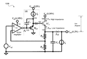
- FIGS. 1A-1B illustrate examples of a low-power low-dropout (LDO) voltage regulator device 100 A in accordance with one or more implementations of the subject technology.
- the LDO voltage regulator device 100 A (hereinafter “device 100 A”) includes an error amplifier 110 , a level-shifter circuit 120 and a pass transistor M N (e.g., a NMOS pass transistor M N , hereinafter “transistor M N ”).
- the error amplifier 110 compares a sampled portion of a regulated output voltage V out (e.g., 1.2 V) of the LDO voltage regulator device 110 A with a reference voltage V ref and generates an error signal 112 .
- the level-shifter circuit 120 is coupled to the error amplifier 110 , and can shift a voltage level of the error signal 112 to facilitate the low dropout operation of the transistor M N .
- a gate node 140 of the transistor M N is coupled to the level-shifter circuit.
- the regulated output voltage V out can be provided at a source node 142 of the transistor M N .
- An advantage of using the transistor M N is that the regulated output voltage V out can be provided with low dropout (e.g., 0.15V) and high power-supply rejection (PSR). Further, a low output impedance of the transistor M N (e.g., at node 142 ) can result in a high unity-gain-bandwidth (UGB) performance of the device 100 A, which can improve the settling time of the device 100 A by more than approximately 60%, for both dips and overshoots of the output voltage.
- UGB unity-gain-bandwidth
- the sampled portion of the regulated output voltage V out that is compared by the reference voltage V ref is generated by a voltage divider formed by the resistors R f1 and R f2 .
- the load capacitor C L in conjunction with the resistors R f1 and R f2 , provides low-pass filtering of the regulated output voltage V out and can include a capacitance of the load.
- the load current is shown as a current source i L in parallel with load capacitor C L .
- the level-shifter circuit 120 of an LDO voltage regulator device 100 B includes a source follower circuit.
- the level-shifter circuit 120 can provide the suitable level shift to properly bias the transistor M N .
- the voltage at the gate node 140 of the transistor M N equals V gsN +V out , and the level-shifter circuit 120 can provide such a voltage.
- An auxiliary supply voltage V aux (e.g., at 2.5 V) has to be used to provide the sufficient voltage at the gate node 140 .
- the source follower circuit can be formed by a transistor M LS (e.g., a PMOS transistor M LS , hereinafter “transistor M LS ”), a compensation capacitor C c , and a current source I b .
- the current source I b is coupled between a source node 124 of the transistor M LS and an auxiliary supply voltage V aux (e.g., at 2.5 V) and provide a bias current for the source node 124 of the transistor M LS .
- a power supply node 114 of the error amplifier 110 and a drain node 144 of the transistor MN can be coupled to a low-dropout input voltage supply (Vin, e.g., at 1.35 V) of the device 100 B.
- Vin low-dropout input voltage supply
- the gate voltage Vg, at the node 140 contributes to a non-dominant pole (P nd ), a large biasing current (e.g., I b ) is needed to push this pole far away from loop's UGB to guarantee a reliable stability.
- the large biasing current I b can result in additional power consumption of the level-shifter circuit 120 , which is undesirable.
- the subject technology avoids using a large biasing current I b , by using the compensation capacitor C c .
- the compensation capacitor C c is coupled between a gate node 122 and the source node 124 of the transistor M LS .
- the compensation capacitor C c allows low-current operation of the level-shifter circuit 120 .
- the low-current operation is made possible by cancellation of a p nd at the gate node 140 of the transistor M N , which is connected to the source node 124 of the transistor M LS .
- the high PSR (e.g., approximately 10 dB at 100 MHz) performance of the devices 100 A and 100 B can be supported by the high input impedance of the transistor M N (e.g., at node 144 ).
- the high input impedance e.g., 1/g dsN
- the high PSR performance is highly important for rejection of power supply ripples, which can adversely affect proper operation of radio-frequency (RF) and analog signal circuitry.
- the subject technology provides the high PSR performance while consuming significantly lower power than the existing high PSR solutions, and having a substantially lower settling time (e.g., approximately 60% lower dip and overshoot settling time).
- the lower settling time is a result of the high UGB performance.
- the high UGB performance of the devices 100 A and 100 B can be understood by the low output impedance of the transistor M N .
- the output impedance of the transistor M N as seen from the source node 142 of the transistor M N , is defined by 1/g mN , which with suitable biasing of the transistor M N , can be sufficiently small to warrant a high UGB performance of the devices 100 A and 100 B.
- Existing solutions using PMOS pass transistor, instead of the NMOS pass transistor M N suffer from large output impedance (e.g., 1/g dsP of the PMOS pass transistor), which results in a low UGB performance and a long settling time.
- FIG. 2 illustrates an example of a low-power LDO voltage regulator device 200 including a fast loop in accordance with one or more implementations of the subject technology.
- the low-power LDO voltage regulator device 200 (hereinafter “device 200 ”) is similar to the device 100 A, except for the addition of the fast loop as described herein.
- the fast loop includes a current mirror 210 coupled to the level-shifter circuit 120 (e.g., to the source node 124 of the transistor M LS ) and a gain boosting circuit 220 .
- the fast loop can improve the transient response-time and the slew rate of the device 200 .
- the current I 3 is approximately equal to the current source I DC .
- the fast loop consumes very low DC current, as the biasing current I 4 can be a small current, due to the use of the compensation capacitance C c , as discussed above.
- the gain boosting circuit 220 includes a gain boosting amplifier 222 coupled to a gate node of a transistor M 2 (e.g., an NMOS transistor).
- the gain boosting amplifier 222 is biased by the input supply voltage Vin (e.g., 1.35V).
- the gain boosting circuit 220 can increase the fast loop bandwidth, thereby improving the transient response-time and the slew rate of the device 200 .
- a coupling capacitor C SR is used by the fast loop to sense undesirable transients (e.g., dips or overshoots) in the regulated output voltage (e.g., V out ).
- the gain boosting circuit 220 can adjust a source current provided to the level-shifter circuit (e.g., the source node of the transistor M LS ) by adding a transient current component i tran to the biasing current I 4 .
- the transient current component i tran can substantially suppress dips and overshoot of the regulated output voltage.
- FIG. 3 illustrates an example of a method 300 for providing a low-power LDO voltage regulator device in accordance with one or more implementations of the subject technology.
- the example method 300 is described herein with reference to, but is not limited to, the device 100 A of FIG. 1A .
- the blocks of the example method 300 are described herein as occurring in serial, or linearly. However, multiple blocks of the example method 300 can occur in parallel.
- the blocks of the example method 300 need not be performed in the order shown and/or one or more of the blocks of the example method 300 need not be performed.
- the methods 300 includes configuring an error amplifier (e.g., 110 of FIG. 1A ) to compare a sampled portion (e.g., sampled by 130 of FIG. 1A ) of a regulated output voltage (e.g., Vout of FIG. 1A ) of the LDO voltage regulator (e.g., 100 A of FIG. 1A ) with a reference voltage (e.g., Vref of FIG. 1A ) and to generate an error signal (e.g., 112 of FIG. 1A ) ( 310 ).
- a level-shifter circuit (e.g., 120 of FIGS. 1A-1B ) may be coupled to the error amplifier ( 320 ).
- An NMOS pass transistor e.g., M N of FIG. 1A
- the level-shifter circuit is configured to shift a voltage level of the error signal to facilitate the low dropout operation of the NMOS pass transistor ( 340 ).
- FIG. 4 illustrates an example of a wireless communication device 400 in accordance with one or more implementations of the subject technology.
- the wireless communication device 400 can comprise a radio-frequency (RF) antenna 410 , a receiver 420 , a transmitter 430 , a baseband processing module 440 , a memory 450 , a processor 460 , a local oscillator generator (LOGEN) 470 , and a power supply 480 .
- RF radio-frequency
- RF radio-frequency
- the RF antenna 410 can be suitable for transmitting and/or receiving RF signals (e.g., wireless signals) over a wide range of frequencies. Although a single RF antenna 410 is illustrated, the subject technology is not so limited.
- the receiver 420 comprises suitable logic circuitry and/or code that can be operable to receive and process signals from the RF antenna 410 .
- the receiver 420 may, for example, be operable to amplify and/or down-covert received wireless signals.
- the receiver 420 is operable to cancel noise in received signals and can be linear over a wide range of frequencies. In this manner, the receiver 420 is suitable for receiving signals in accordance with a variety of wireless standards. Wi-Fi, WiMAX, Bluetooth, and various cellular standards.
- the transmitter 430 comprises suitable logic circuitry and/or code that can be operable to process and transmit signals from the RF antenna 410 .
- the transmitter 430 may, for example, be operable to up-covert baseband signals to RF signals and amplify RF signals.
- the transmitter 430 is operable to up-convert and to amplify baseband signals processed in accordance with a variety of wireless standards. Examples of such standards include Wi-Fi, WiMAX, Bluetooth, and various cellular standards.
- the transmitter 430 is operable to provide signals for further amplification by one or more power amplifiers.
- the duplexer 412 provides isolation in the transmit band to avoid saturation of the receiver 420 or damaging parts of the receiver 420 , and to relax one or more design requirements of the receiver 420 . Furthermore, the duplexer 412 can attenuate the noise in the receive band.
- the duplexer is operable in multiple frequency bands of various wireless standards.
- the baseband processing module 440 comprises suitable logic, circuitry, interfaces, and/or code that can be operable to perform processing of baseband signals.
- the baseband processing module 440 may, for example, analyze received signals and generate control and/or feedback signals for configuring various components of the wireless communication device 400 such as the receiver 420 .
- the baseband processing module 440 is operable to encode, decode, transcode, modulate, demodulate, encrypt, decrypt, scramble, descramble, and/or otherwise process data in accordance with one or more wireless standards.
- the processor 460 comprises suitable logic, circuitry, and/or code that can enable processing data and/or controlling operations of the wireless communication device 400 .
- the processor 460 is enabled to provide control signals to various other portions of the wireless communication device 400 .
- the processor 460 can also control transfers of data between various portions of the wireless communication device 400 .
- the processor 460 can enable implementation of an operating system or otherwise execute code to manage operations of the wireless communication device 400 .
- the memory 450 comprises suitable logic, circuitry, and/or code that can enable storage of various types of information such as received data, generated data, code, and/or configuration information.
- the local oscillator generator (LOG EN) 470 comprises suitable logic, circuitry, interfaces, and/or code that can be operable to generate one or more oscillating signals of one or more frequencies.
- the LOGEN 470 can be operable to generate digital and/or analog signals. In this manner, the LOGEN 470 can be operable to generate one or more clock signals and/or sinusoidal signals. Characteristics of the oscillating signals such as the frequency and duty cycle can be determined based on one or more control signals from, for example, the processor 460 and/or the baseband processing module 440 .
- the processor 460 can configure the various components of the wireless communication device 400 based on a wireless standard according to which it is desired to receive signals.
- Wireless signals can be received via the RF antenna 410 and amplified and down-converted by the receiver 420 .
- the baseband processing module 440 can perform noise estimation and/or noise cancellation, decoding, and/or demodulation of the baseband signals. In this manner, information in the received signal can be recovered and utilized appropriately. For example, the information can be audio and/or video to be presented to a user of the wireless communication device, data to be stored to the memory 450 , and/or information affecting and/or enabling operation of the wireless communication device 400 .
- the baseband processing module 440 can modulate, encode and perform other processing on audio, video, and/or control signals to be transmitted by the transmitter 430 in accordance to various wireless standards.
- the power supply 480 can provide one or more regulated rail voltages (e.g., V DD ) for various circuitries of the wireless communication device 400 .
- the power supply 480 can include a low-power low-dropout (LDO) voltage regulator device (e.g., 100 B of FIG. 1B ) of the subject technology.
- the power supply 480 can include a low-power low-dropout (LDO) voltage regulator device with a low-current fast loop (e.g., see 200 of FIG. 2 ) disclosed above, which can improve a transient response-time and a slew rate of the power supply 480 .
- LDO low-power low-dropout
- the phrase “at least one of” preceding a series of items, with the term “and” or “or” to separate any of the items, modifies the list as a whole, rather than each member of the list (i.e., each item).
- the phrase “at least one of” does not require selection of at least one of each item listed; rather, the phrase allows a meaning that includes at least one of any one of the items, and/or at least one of any combination of the items, and/or at least one of each of the items.
- phrases “at least one of A, B, and C” or “at least one of A, B, or C” each refer to only A, only B, or only C; any combination of A, B, and C; and/or at least one of each of A, B, and C.
- a phrase such as “an aspect” does not imply that such aspect is essential to the subject technology or that such aspect applies to all configurations of the subject technology.
- a disclosure relating to an aspect can apply to all configurations, or one or more configurations.
- An aspect can provide one or more examples of the disclosure.
- a phrase such as an “aspect” refers to one or more aspects and vice versa.
- a phrase such as an “embodiment” does not imply that such embodiment is essential to the subject technology or that such embodiment applies to all configurations of the subject technology.
- a disclosure relating to an embodiment can apply to all embodiments, or one or more embodiments.
- An embodiment can provide one or more examples of the disclosure.
- a phrase such an “embodiment” can refer to one or more embodiments and vice versa.
- a phrase such as a “configuration” does not imply that such configuration is essential to the subject technology or that such configuration applies to all configurations of the subject technology.
- a disclosure relating to a configuration can apply to all configurations, or one or more configurations.
- a configuration can provide one or more examples of the disclosure.
- a phrase such as a “configuration” can refer to one or more configurations and vice versa.
Landscapes
- Engineering & Computer Science (AREA)
- Physics & Mathematics (AREA)
- Electromagnetism (AREA)
- General Physics & Mathematics (AREA)
- Radar, Positioning & Navigation (AREA)
- Automation & Control Theory (AREA)
- Continuous-Control Power Sources That Use Transistors (AREA)
Abstract
Description
Claims (20)
Priority Applications (2)
| Application Number | Priority Date | Filing Date | Title |
|---|---|---|---|
| US14/173,742 US9753474B2 (en) | 2014-01-14 | 2014-02-05 | Low-power low-dropout voltage regulators with high power supply rejection and fast settling performance |
| EP14004369.6A EP2894538A3 (en) | 2014-01-14 | 2014-12-22 | Low-power low-dropout voltage regulators with high power supply rejection and fast settling performance |
Applications Claiming Priority (2)
| Application Number | Priority Date | Filing Date | Title |
|---|---|---|---|
| US201461927427P | 2014-01-14 | 2014-01-14 | |
| US14/173,742 US9753474B2 (en) | 2014-01-14 | 2014-02-05 | Low-power low-dropout voltage regulators with high power supply rejection and fast settling performance |
Publications (2)
| Publication Number | Publication Date |
|---|---|
| US20150198960A1 US20150198960A1 (en) | 2015-07-16 |
| US9753474B2 true US9753474B2 (en) | 2017-09-05 |
Family
ID=52133791
Family Applications (1)
| Application Number | Title | Priority Date | Filing Date |
|---|---|---|---|
| US14/173,742 Active 2035-04-19 US9753474B2 (en) | 2014-01-14 | 2014-02-05 | Low-power low-dropout voltage regulators with high power supply rejection and fast settling performance |
Country Status (2)
| Country | Link |
|---|---|
| US (1) | US9753474B2 (en) |
| EP (1) | EP2894538A3 (en) |
Cited By (5)
| Publication number | Priority date | Publication date | Assignee | Title |
|---|---|---|---|---|
| US20170220059A1 (en) * | 2016-01-29 | 2017-08-03 | Kabushiki Kaisha Toshiba | Regulator circuit |
| US9960737B1 (en) | 2017-03-06 | 2018-05-01 | Psemi Corporation | Stacked PA power control |
| US9998075B1 (en) * | 2017-01-25 | 2018-06-12 | Psemi Corporation | LDO with fast recovery from saturation |
| CN109976424A (en) * | 2019-04-18 | 2019-07-05 | 电子科技大学 | A kind of non-capacitive low-dropout linear voltage regulator |
| US10873257B2 (en) | 2018-11-07 | 2020-12-22 | Regents Of The University Of Minnesota | Low dropout regulator with smart offset |
Families Citing this family (43)
| Publication number | Priority date | Publication date | Assignee | Title |
|---|---|---|---|---|
| US9454168B2 (en) * | 2014-06-16 | 2016-09-27 | Linear Technology Corporation | LDO regulator powered by its regulated output voltage for high PSRR |
| US9817415B2 (en) * | 2015-07-15 | 2017-11-14 | Qualcomm Incorporated | Wide voltage range low drop-out regulators |
| US9753476B1 (en) | 2016-03-03 | 2017-09-05 | Sandisk Technologies Llc | Voltage regulator with fast overshoot settling response |
| US9778672B1 (en) | 2016-03-31 | 2017-10-03 | Qualcomm Incorporated | Gate boosted low drop regulator |
| US9806759B1 (en) * | 2016-07-01 | 2017-10-31 | Intel IP Corporation | Low drop out compensation technique for reduced dynamic errors in digital-to-time converters |
| US10014772B2 (en) | 2016-08-03 | 2018-07-03 | Nxp B.V. | Voltage regulator |
| US9791874B1 (en) | 2016-11-04 | 2017-10-17 | Nxp B.V. | NMOS-based voltage regulator |
| KR102032327B1 (en) * | 2016-11-22 | 2019-10-15 | 에스케이하이닉스 주식회사 | Digital low drop-out regulator and resistive change memory device using it |
| EP3379369B1 (en) | 2017-03-23 | 2021-05-26 | ams AG | Low-dropout regulator having reduced regulated output voltage spikes |
| US10234883B1 (en) * | 2017-12-18 | 2019-03-19 | Apple Inc. | Dual loop adaptive LDO voltage regulator |
| WO2019136299A1 (en) | 2018-01-05 | 2019-07-11 | Atlazo, Inc. | Power management system |
| US10614184B2 (en) | 2018-01-08 | 2020-04-07 | Atlazo, Inc. | Semiconductor process and performance sensor |
| US10635130B2 (en) | 2018-02-01 | 2020-04-28 | Atlazo, Inc. | Process, voltage and temperature tolerant clock generator |
| US10571945B2 (en) * | 2018-02-21 | 2020-02-25 | Atlazo, Inc. | Low power regulator circuits, systems and methods regarding the same |
| US10700604B2 (en) | 2018-03-07 | 2020-06-30 | Atlazo, Inc. | High performance switch devices and methods for operating the same |
| US10411599B1 (en) | 2018-03-28 | 2019-09-10 | Qualcomm Incorporated | Boost and LDO hybrid converter with dual-loop control |
| CN108616260B (en) * | 2018-04-02 | 2022-05-10 | 广州慧智微电子股份有限公司 | Power supply circuit of power amplifier |
| US10444780B1 (en) | 2018-09-20 | 2019-10-15 | Qualcomm Incorporated | Regulation/bypass automation for LDO with multiple supply voltages |
| US10591938B1 (en) * | 2018-10-16 | 2020-03-17 | Qualcomm Incorporated | PMOS-output LDO with full spectrum PSR |
| US10545523B1 (en) | 2018-10-25 | 2020-01-28 | Qualcomm Incorporated | Adaptive gate-biased field effect transistor for low-dropout regulator |
| US11372436B2 (en) | 2019-10-14 | 2022-06-28 | Qualcomm Incorporated | Simultaneous low quiescent current and high performance LDO using single input stage and multiple output stages |
| EP3812872B1 (en) * | 2019-10-25 | 2023-06-14 | Nxp B.V. | A system comprising a low drop-out regulator |
| EP3832428B1 (en) * | 2019-12-04 | 2023-07-19 | Nxp B.V. | Apparatuses and methods involving switching between dual inputs of power amplication circuitry |
| CN111290460B (en) * | 2020-02-25 | 2021-08-06 | 电子科技大学 | A Low Dropout Linear Regulator with High Power Supply Rejection Ratio and Fast Transient Response |
| CN111474975B (en) * | 2020-05-18 | 2021-08-31 | 成都市易冲半导体有限公司 | Output current sampling circuit of LDO (low dropout regulator) and sampling precision adjusting method |
| CN111665894B (en) * | 2020-06-23 | 2021-04-02 | 上海安路信息科技股份有限公司 | Low dropout voltage regulator |
| US12276993B2 (en) | 2020-07-24 | 2025-04-15 | Qualcomm Incorporated | Charge pump based low dropout regulator |
| CN112068627B (en) * | 2020-09-11 | 2021-04-09 | 杭州万高科技股份有限公司 | Voltage output regulating module |
| CN112286334B (en) * | 2020-10-30 | 2021-07-23 | 广州鸿博微电子技术有限公司 | Low-power power switching circuit for MCU and its realization method |
| US11561563B2 (en) | 2020-12-11 | 2023-01-24 | Skyworks Solutions, Inc. | Supply-glitch-tolerant regulator |
| US11817854B2 (en) | 2020-12-14 | 2023-11-14 | Skyworks Solutions, Inc. | Generation of positive and negative switch gate control voltages |
| US11556144B2 (en) * | 2020-12-16 | 2023-01-17 | Skyworks Solutions, Inc. | High-speed low-impedance boosting low-dropout regulator |
| US11295787B1 (en) * | 2020-12-28 | 2022-04-05 | Nxp B.V. | Reducing SRAM leakage using scalable switched capacitor regulators |
| US11687104B2 (en) * | 2021-03-25 | 2023-06-27 | Qualcomm Incorporated | Power supply rejection enhancer |
| US11502683B2 (en) | 2021-04-14 | 2022-11-15 | Skyworks Solutions, Inc. | Calibration of driver output current |
| CN114578884B (en) * | 2021-05-03 | 2024-02-02 | 宁波奥拉半导体股份有限公司 | Linear voltage regulator and system with same |
| US12045073B2 (en) | 2021-05-03 | 2024-07-23 | Ningbo Aura Semiconductor Co., Limited | Enabling fast transient response in a linear regulator when loop-gain reduction is employed for frequency compensation |
| US11906998B2 (en) * | 2021-09-23 | 2024-02-20 | Apple Inc. | NMOS super source follower low dropout regulator |
| US12068687B2 (en) | 2021-10-15 | 2024-08-20 | Advanced Micro Devices, Inc. | Method to reduce overshoot in a voltage regulating power supply |
| CN118226913A (en) * | 2022-12-21 | 2024-06-21 | 川能电子有限公司 | Dual-loop linear regulator and stability compensation circuit and control method thereof |
| CN116166083B (en) * | 2023-04-23 | 2023-07-21 | 盈力半导体(上海)有限公司 | Low dropout linear voltage stabilizing circuit and buck circuit |
| CN116301181B (en) * | 2023-05-16 | 2023-07-21 | 上海灵动微电子股份有限公司 | Overshoot suppression circuit for load jump of low-dropout linear voltage regulator |
| CN119002615B (en) * | 2024-10-25 | 2025-01-24 | 成都市易冲半导体有限公司 | A low voltage drop linear regulator and electronic equipment |
Citations (11)
| Publication number | Priority date | Publication date | Assignee | Title |
|---|---|---|---|---|
| US6225857B1 (en) * | 2000-02-08 | 2001-05-01 | Analog Devices, Inc. | Non-inverting driver circuit for low-dropout voltage regulator |
| US6556083B2 (en) * | 2000-12-15 | 2003-04-29 | Semiconductor Components Industries Llc | Method and apparatus for maintaining stability in a circuit under variable load conditions |
| US20040080367A1 (en) * | 2002-10-29 | 2004-04-29 | Crain Ethan A. | Low power low voltage differential signal receiver with improved skew and jitter performance |
| US20100156362A1 (en) * | 2008-12-23 | 2010-06-24 | Texas Instruments Incorporated | Load transient response time of LDOs with NMOS outputs with a voltage controlled current source |
| US20110156670A1 (en) | 2009-12-29 | 2011-06-30 | Texas Instruments Incorporated | Passive bootstrapped charge pump for nmos power device based regulators |
| US20120176107A1 (en) | 2011-01-11 | 2012-07-12 | Freescale Semiconductor, Inc | Ldo linear regulator with improved transient response |
| US20130063637A1 (en) * | 2011-09-12 | 2013-03-14 | Sony Corporation | Solid-state image pickup device and camera system |
| US20130176006A1 (en) | 2012-01-06 | 2013-07-11 | Micrel, Inc. | High Bandwidth PSRR Power Supply Regulator |
| US8604762B2 (en) * | 2006-05-25 | 2013-12-10 | Texas Instruments Incorporated | Low noise, low dropout regulators |
| US20140340067A1 (en) * | 2013-05-14 | 2014-11-20 | Intel IP Corporation | Output voltage variation reduction |
| US8953364B2 (en) * | 2012-09-18 | 2015-02-10 | Micron Technology, Inc. | Voltage rail noise sensing circuit and method |
-
2014
- 2014-02-05 US US14/173,742 patent/US9753474B2/en active Active
- 2014-12-22 EP EP14004369.6A patent/EP2894538A3/en not_active Withdrawn
Patent Citations (11)
| Publication number | Priority date | Publication date | Assignee | Title |
|---|---|---|---|---|
| US6225857B1 (en) * | 2000-02-08 | 2001-05-01 | Analog Devices, Inc. | Non-inverting driver circuit for low-dropout voltage regulator |
| US6556083B2 (en) * | 2000-12-15 | 2003-04-29 | Semiconductor Components Industries Llc | Method and apparatus for maintaining stability in a circuit under variable load conditions |
| US20040080367A1 (en) * | 2002-10-29 | 2004-04-29 | Crain Ethan A. | Low power low voltage differential signal receiver with improved skew and jitter performance |
| US8604762B2 (en) * | 2006-05-25 | 2013-12-10 | Texas Instruments Incorporated | Low noise, low dropout regulators |
| US20100156362A1 (en) * | 2008-12-23 | 2010-06-24 | Texas Instruments Incorporated | Load transient response time of LDOs with NMOS outputs with a voltage controlled current source |
| US20110156670A1 (en) | 2009-12-29 | 2011-06-30 | Texas Instruments Incorporated | Passive bootstrapped charge pump for nmos power device based regulators |
| US20120176107A1 (en) | 2011-01-11 | 2012-07-12 | Freescale Semiconductor, Inc | Ldo linear regulator with improved transient response |
| US20130063637A1 (en) * | 2011-09-12 | 2013-03-14 | Sony Corporation | Solid-state image pickup device and camera system |
| US20130176006A1 (en) | 2012-01-06 | 2013-07-11 | Micrel, Inc. | High Bandwidth PSRR Power Supply Regulator |
| US8953364B2 (en) * | 2012-09-18 | 2015-02-10 | Micron Technology, Inc. | Voltage rail noise sensing circuit and method |
| US20140340067A1 (en) * | 2013-05-14 | 2014-11-20 | Intel IP Corporation | Output voltage variation reduction |
Non-Patent Citations (2)
| Title |
|---|
| Easwaran, "A Low Power NMOS LDO in the Philips CO50PMU Process," Mar. 2006, Masters Thesis, University of Twente, retrieved from http://eprints.eemcs.utwente.nl/8601/01/Easwaran-S.-Navaneeth.-MSc2006-A-Low-Power-NMOS-LDO-in-the-Philips-CO50PMU-Process.pdf. |
| Easwaran, "A Low Power NMOS LDO in the Philips CO50PMU Process," Mar. 2006, Masters Thesis, University of Twente, retrieved from http://eprints.eemcs.utwente.nl/8601/01/Easwaran—S.—Navaneeth.—MSc2006—A—Low—Power—NMOS—LDO—in—the—Philips—CO50PMU—Process.pdf. |
Cited By (6)
| Publication number | Priority date | Publication date | Assignee | Title |
|---|---|---|---|---|
| US20170220059A1 (en) * | 2016-01-29 | 2017-08-03 | Kabushiki Kaisha Toshiba | Regulator circuit |
| US9998075B1 (en) * | 2017-01-25 | 2018-06-12 | Psemi Corporation | LDO with fast recovery from saturation |
| US9960737B1 (en) | 2017-03-06 | 2018-05-01 | Psemi Corporation | Stacked PA power control |
| US10873257B2 (en) | 2018-11-07 | 2020-12-22 | Regents Of The University Of Minnesota | Low dropout regulator with smart offset |
| CN109976424A (en) * | 2019-04-18 | 2019-07-05 | 电子科技大学 | A kind of non-capacitive low-dropout linear voltage regulator |
| CN109976424B (en) * | 2019-04-18 | 2020-07-31 | 电子科技大学 | Non-capacitor type low dropout linear voltage regulator |
Also Published As
| Publication number | Publication date |
|---|---|
| US20150198960A1 (en) | 2015-07-16 |
| EP2894538A3 (en) | 2015-08-05 |
| EP2894538A2 (en) | 2015-07-15 |
Similar Documents
| Publication | Publication Date | Title |
|---|---|---|
| US9753474B2 (en) | Low-power low-dropout voltage regulators with high power supply rejection and fast settling performance | |
| US9225234B2 (en) | In-rush current control for charge-pump LDO | |
| US9837993B2 (en) | Voltage generator with charge pump and related methods and apparatus | |
| US11726513B2 (en) | On-chip dual-supply multi-mode CMOS regulators | |
| EP3031135B1 (en) | Analog switch for rf front end | |
| US7956682B2 (en) | Amplifier | |
| US8989688B2 (en) | Low-noise TIA-to-ADC interface with a wide-range of passive gain control | |
| US9246438B2 (en) | Receiver architecture for a compact and low power receiver | |
| EP3262479A1 (en) | Transmit digital to analog converter (dac) spur attenuation | |
| US8626092B2 (en) | Low variation current multiplier | |
| US12045073B2 (en) | Enabling fast transient response in a linear regulator when loop-gain reduction is employed for frequency compensation | |
| US9160388B2 (en) | Receiver architecture with complementary passive mixer and complementary common-gate tia with low-noise gain control | |
| US9325313B2 (en) | Low-power level-shift circuit for data-dependent signals | |
| US20200144927A1 (en) | Dual-comparator current-mode rectifier | |
| US10270348B2 (en) | Synchronous switching regulator circuit | |
| JP4887470B2 (en) | Voltage regulator with shunt feedback | |
| US9331655B2 (en) | Pop-click noise grounding switch design with deep sub-micron CMOS technology | |
| US10476400B1 (en) | Dual-comparator current-mode rectifier | |
| US20080181144A1 (en) | RF transceiver system with impedance mismatch detection and control and methods for use therewith | |
| US9411387B2 (en) | Pre-charging mechanism for multi-input switching charger | |
| US20080182625A1 (en) | RF transeiver system with antenna configuration control and methods for use therewith | |
| US7518421B1 (en) | System and method for providing a kick back compensated charge pump with kicker capacitor |
Legal Events
| Date | Code | Title | Description |
|---|---|---|---|
| AS | Assignment |
Owner name: BROADCOM CORPORATION, CALIFORNIA Free format text: ASSIGNMENT OF ASSIGNORS INTEREST;ASSIGNORS:ZHANG, JINGHUA;SETIAWAN, RICKY;HARRISON, JEFFREY NORWOOD;SIGNING DATES FROM 20140127 TO 20140128;REEL/FRAME:032215/0175 |
|
| AS | Assignment |
Owner name: BANK OF AMERICA, N.A., AS COLLATERAL AGENT, NORTH CAROLINA Free format text: PATENT SECURITY AGREEMENT;ASSIGNOR:BROADCOM CORPORATION;REEL/FRAME:037806/0001 Effective date: 20160201 Owner name: BANK OF AMERICA, N.A., AS COLLATERAL AGENT, NORTH Free format text: PATENT SECURITY AGREEMENT;ASSIGNOR:BROADCOM CORPORATION;REEL/FRAME:037806/0001 Effective date: 20160201 |
|
| AS | Assignment |
Owner name: AVAGO TECHNOLOGIES GENERAL IP (SINGAPORE) PTE. LTD., SINGAPORE Free format text: ASSIGNMENT OF ASSIGNORS INTEREST;ASSIGNOR:BROADCOM CORPORATION;REEL/FRAME:041706/0001 Effective date: 20170120 Owner name: AVAGO TECHNOLOGIES GENERAL IP (SINGAPORE) PTE. LTD Free format text: ASSIGNMENT OF ASSIGNORS INTEREST;ASSIGNOR:BROADCOM CORPORATION;REEL/FRAME:041706/0001 Effective date: 20170120 |
|
| AS | Assignment |
Owner name: BROADCOM CORPORATION, CALIFORNIA Free format text: TERMINATION AND RELEASE OF SECURITY INTEREST IN PATENTS;ASSIGNOR:BANK OF AMERICA, N.A., AS COLLATERAL AGENT;REEL/FRAME:041712/0001 Effective date: 20170119 |
|
| STCF | Information on status: patent grant |
Free format text: PATENTED CASE |
|
| AS | Assignment |
Owner name: AVAGO TECHNOLOGIES INTERNATIONAL SALES PTE. LIMITE Free format text: MERGER;ASSIGNOR:AVAGO TECHNOLOGIES GENERAL IP (SINGAPORE) PTE. LTD.;REEL/FRAME:047422/0464 Effective date: 20180509 |
|
| AS | Assignment |
Owner name: AVAGO TECHNOLOGIES INTERNATIONAL SALES PTE. LIMITE Free format text: CORRECTIVE ASSIGNMENT TO CORRECT THE EXECUTION DATE PREVIOUSLY RECORDED AT REEL: 047422 FRAME: 0464. ASSIGNOR(S) HEREBY CONFIRMS THE MERGER;ASSIGNOR:AVAGO TECHNOLOGIES GENERAL IP (SINGAPORE) PTE. LTD.;REEL/FRAME:048883/0702 Effective date: 20180905 |
|
| MAFP | Maintenance fee payment |
Free format text: PAYMENT OF MAINTENANCE FEE, 4TH YEAR, LARGE ENTITY (ORIGINAL EVENT CODE: M1551); ENTITY STATUS OF PATENT OWNER: LARGE ENTITY Year of fee payment: 4 |
|
| MAFP | Maintenance fee payment |
Free format text: PAYMENT OF MAINTENANCE FEE, 8TH YEAR, LARGE ENTITY (ORIGINAL EVENT CODE: M1552); ENTITY STATUS OF PATENT OWNER: LARGE ENTITY Year of fee payment: 8 |