US9728906B2 - Power adapter with a single-piece insulator assembly - Google Patents
Power adapter with a single-piece insulator assembly Download PDFInfo
- Publication number
- US9728906B2 US9728906B2 US15/156,629 US201615156629A US9728906B2 US 9728906 B2 US9728906 B2 US 9728906B2 US 201615156629 A US201615156629 A US 201615156629A US 9728906 B2 US9728906 B2 US 9728906B2
- Authority
- US
- United States
- Prior art keywords
- electrical assembly
- connector
- power adapter
- electrical
- voltage
- Prior art date
- Legal status (The legal status is an assumption and is not a legal conclusion. Google has not performed a legal analysis and makes no representation as to the accuracy of the status listed.)
- Expired - Fee Related
Links
Images


Classifications
-
- H—ELECTRICITY
- H01—ELECTRIC ELEMENTS
- H01R—ELECTRICALLY-CONDUCTIVE CONNECTIONS; STRUCTURAL ASSOCIATIONS OF A PLURALITY OF MUTUALLY-INSULATED ELECTRICAL CONNECTING ELEMENTS; COUPLING DEVICES; CURRENT COLLECTORS
- H01R13/00—Details of coupling devices of the kinds covered by groups H01R12/70 or H01R24/00 - H01R33/00
- H01R13/66—Structural association with built-in electrical component
- H01R13/665—Structural association with built-in electrical component with built-in electronic circuit
- H01R13/6675—Structural association with built-in electrical component with built-in electronic circuit with built-in power supply
-
- H—ELECTRICITY
- H01—ELECTRIC ELEMENTS
- H01B—CABLES; CONDUCTORS; INSULATORS; SELECTION OF MATERIALS FOR THEIR CONDUCTIVE, INSULATING OR DIELECTRIC PROPERTIES
- H01B17/00—Insulators or insulating bodies characterised by their form
- H01B17/56—Insulating bodies
- H01B17/64—Insulating bodies with conductive admixtures, inserts or layers
-
- H—ELECTRICITY
- H01—ELECTRIC ELEMENTS
- H01R—ELECTRICALLY-CONDUCTIVE CONNECTIONS; STRUCTURAL ASSOCIATIONS OF A PLURALITY OF MUTUALLY-INSULATED ELECTRICAL CONNECTING ELEMENTS; COUPLING DEVICES; CURRENT COLLECTORS
- H01R13/00—Details of coupling devices of the kinds covered by groups H01R12/70 or H01R24/00 - H01R33/00
- H01R13/66—Structural association with built-in electrical component
- H01R13/665—Structural association with built-in electrical component with built-in electronic circuit
-
- H—ELECTRICITY
- H01—ELECTRIC ELEMENTS
- H01R—ELECTRICALLY-CONDUCTIVE CONNECTIONS; STRUCTURAL ASSOCIATIONS OF A PLURALITY OF MUTUALLY-INSULATED ELECTRICAL CONNECTING ELEMENTS; COUPLING DEVICES; CURRENT COLLECTORS
- H01R31/00—Coupling parts supported only by co-operation with counterpart
- H01R31/06—Intermediate parts for linking two coupling parts, e.g. adapter
- H01R31/065—Intermediate parts for linking two coupling parts, e.g. adapter with built-in electric apparatus
-
- H—ELECTRICITY
- H01—ELECTRIC ELEMENTS
- H01R—ELECTRICALLY-CONDUCTIVE CONNECTIONS; STRUCTURAL ASSOCIATIONS OF A PLURALITY OF MUTUALLY-INSULATED ELECTRICAL CONNECTING ELEMENTS; COUPLING DEVICES; CURRENT COLLECTORS
- H01R4/00—Electrically-conductive connections between two or more conductive members in direct contact, i.e. touching one another; Means for effecting or maintaining such contact; Electrically-conductive connections having two or more spaced connecting locations for conductors and using contact members penetrating insulation
- H01R4/70—Insulation of connections
-
- H—ELECTRICITY
- H02—GENERATION; CONVERSION OR DISTRIBUTION OF ELECTRIC POWER
- H02M—APPARATUS FOR CONVERSION BETWEEN AC AND AC, BETWEEN AC AND DC, OR BETWEEN DC AND DC, AND FOR USE WITH MAINS OR SIMILAR POWER SUPPLY SYSTEMS; CONVERSION OF DC OR AC INPUT POWER INTO SURGE OUTPUT POWER; CONTROL OR REGULATION THEREOF
- H02M7/00—Conversion of AC power input into DC power output; Conversion of DC power input into AC power output
- H02M7/003—Constructional details, e.g. physical layout, assembly, wiring or busbar connections
-
- H—ELECTRICITY
- H02—GENERATION; CONVERSION OR DISTRIBUTION OF ELECTRIC POWER
- H02M—APPARATUS FOR CONVERSION BETWEEN AC AND AC, BETWEEN AC AND DC, OR BETWEEN DC AND DC, AND FOR USE WITH MAINS OR SIMILAR POWER SUPPLY SYSTEMS; CONVERSION OF DC OR AC INPUT POWER INTO SURGE OUTPUT POWER; CONTROL OR REGULATION THEREOF
- H02M7/00—Conversion of AC power input into DC power output; Conversion of DC power input into AC power output
- H02M7/02—Conversion of AC power input into DC power output without possibility of reversal
- H02M7/04—Conversion of AC power input into DC power output without possibility of reversal by static converters
-
- H—ELECTRICITY
- H01—ELECTRIC ELEMENTS
- H01R—ELECTRICALLY-CONDUCTIVE CONNECTIONS; STRUCTURAL ASSOCIATIONS OF A PLURALITY OF MUTUALLY-INSULATED ELECTRICAL CONNECTING ELEMENTS; COUPLING DEVICES; CURRENT COLLECTORS
- H01R13/00—Details of coupling devices of the kinds covered by groups H01R12/70 or H01R24/00 - H01R33/00
- H01R13/46—Bases; Cases
- H01R13/502—Bases; Cases composed of different pieces
- H01R13/504—Bases; Cases composed of different pieces different pieces being moulded, cemented, welded, e.g. ultrasonic welding, or swaged together
-
- H—ELECTRICITY
- H01—ELECTRIC ELEMENTS
- H01R—ELECTRICALLY-CONDUCTIVE CONNECTIONS; STRUCTURAL ASSOCIATIONS OF A PLURALITY OF MUTUALLY-INSULATED ELECTRICAL CONNECTING ELEMENTS; COUPLING DEVICES; CURRENT COLLECTORS
- H01R13/00—Details of coupling devices of the kinds covered by groups H01R12/70 or H01R24/00 - H01R33/00
- H01R13/66—Structural association with built-in electrical component
- H01R13/6608—Structural association with built-in electrical component with built-in single component
- H01R13/6633—Structural association with built-in electrical component with built-in single component with inductive component, e.g. transformer
Definitions
- Power adapters are ubiquitous and are used in a variety of electronic devices. Some power adapters convert an incoming AC voltage into a DC voltage for use be a connected electronic devices. Some other power adapters convert an AC waveform to another AC waveform, where the output voltage and frequency can be set arbitrarily. Most electronic devices operate on a DC voltage. Examples of electronic devices include but are not limited to computers, portable media players, tablets, mobile phones, etc.
- a transformer converts the incoming AC power to DC power and associated circuitry may filter and regulate the DC to a desired value.
- Each of the individual components of a basic conventional AC-DC adapter is well-known in the art.
- insulator material is provided between the high-voltage circuitry of the adapter (e.g., AC voltage) and the low voltage circuitry (e.g., DC voltage). The insulator material helps to protect the low voltage circuitry from being affected by malfunction in the high voltage circuitry.
- the process of assembling a power adapter includes many manual steps.
- an insulating material such as a Kapton® tape is hand-wrapped around the high-voltage components in order to provide the required insulation.
- a manual process is prone to large variations in quality and reliability, a better process of manufacturing a power adapter will greatly alleviate the quality issues and aid in the manufacturability of the power adapters.
- Other potential problems may be related to the use of separate printed circuit boards (i.e., one for the AC circuit and the other for the DC circuit), in that the boards must be electrically connected to each other prior to final assembly.
- connection wires may need to be hand soldered and because the small components must be held in place in a very small area during the manufacturing process.
- Some attempts at dealing with the potential wiring issues have been made by utilizing ribbon cable.
- Such cables can be bulky, stiff and hard to work with in the small confines of power adaptors. They may, for example, require tape and/or glue to be held in place.
- Embodiments of the present invention are generally related to power adapters. More specifically, some embodiments of the present invention are related to a single-piece insulator assembly that has features and channels embedded therein that assist in quick and accurate assembly of a power adapter.
- the power adapter includes a first connector and a first electrical assembly coupled to the first connector and configured to receive an incoming AC voltage and convert it to a DC voltage.
- the power adapter further includes a second connector and a second electrical assembly coupled to the second connector and configured to accept the DC voltage and output the DC voltage via the second connector.
- the power adapter also includes a single-piece insulator unit that has a first side and a second side.
- the first electrical assembly is coupled to the first side and the second electrical assembly is coupled to the second side.
- the insulator assembly further includes one or more channels embedded within it to provide an electrical path between the first electrical assembly and the second electrical assembly at designated locations.
- the power adapter further includes a power transformer attached to the single-piece insulator unit and a common mode choke attached to the single-piece insulator unit.
- the insulator assembly includes a single-piece structure that has a first side and a second side. Each of the first and the second side has features thereon to enable the single-piece structure to accept a first circuitry and a second circuitry, respectively. There are one or more channels embedded in the single-piece structure. Each of the one or more channels extends from the first side to the second side.
- the single-piece structure further includes electrically conducting members disposed in each of the one or more channels to provide electrical connection between the first circuitry and the second circuitry.
- the single-piece structure is made from a material that has a V-0 flame rating, e.g., glass-filled nylon.
- Some other embodiments of the present invention provide a method for assembling or manufacturing a power adapter.
- the method includes providing a single-piece insulator unit that has a first side and a second side. Each of the first side and the second side includes features that are formed thereon.
- the method further includes attaching a transformer at a first predefined location of the single-piece insulator unit and attaching a common mode choke at a second predefined location of the single-piece insulator unit.
- the method also includes attaching a primary printed circuit board (PCB) including a first circuitry to the first side of the single-piece insulator unit and attaching a secondary PCB including a second circuitry to the second side of the single-piece insulator unit.
- PCB primary printed circuit board
- the method includes providing electrical connectivity between the primary PCB and the secondary PCB.
- the method includes attaching a cap assembly to the single-piece insulator unit, placing the single-piece insulator unit inside housing, and attaching the cap assembly to the housing to seal the single-piece insulator unit within the housing.
- FIGS. 1A and 1B illustrate a power adapter according to an embodiment of the present invention.
- FIG. 2 is a partially exploded view of a power adapter illustrating various top-level components of the power adapter according to an embodiment of the present invention.
- FIGS. 3A and 3B illustrates partial cross-sectional views of the adapter according to an embodiment of the present invention.
- FIG. 4 illustrates an exploded view of the top-level electrical assembly according to an embodiment of the present invention.
- FIG. 5 is an isometric view of the single-piece insulator according to an embodiment of the present invention.
- FIGS. 6A-6J illustrate a process for assembling the power adapter according to an embodiment of the present invention.
- FIGS. 7A and 7B is a flow chart of a process for manufacturing a power adapter corresponding to FIGS. 6A-6J , according to an embodiment of the present invention.
- Embodiments of the present invention are generally related to power adapters. More specifically, some embodiments of the present invention provide a power adapter that includes a single-piece insulator structure.
- the insulator structure includes features that are designed to accept a primary printed circuit board (PCB), a transformer, and a secondary PCB.
- the insulator structure has embedded channels in it and metal members can be inserted in the channels to create an electrical path between the primary PCB and the secondary PCB.
- Power adapters for use with portable electronic devices are disclosed.
- the power adapters disclosed herein can be manufactured in a more efficient and consistent manner that can result in one or more advantages.
- the use of a single-piece insulator assembly results in consistent, reliable and adequate spacing between the primary and secondary circuits such that the power adapters consistently meet or exceed the required safety tolerances.
- the use of conductive pins/members instead of wires, as described below, to electrically couple the primary and secondary stages together also results in reduced manufacturing requirements and more consistently manufactured and reliable end products.
- inventions of the present invention provide method for manufacturing a power adapter.
- the method includes providing a single-piece insulator structure that has embedded electrical pathways that extend from one side to another side of the insulator structure.
- a common mode choke, a transformer, a primary PCB that includes high-voltage (e.g., AC) circuitry, and a secondary PCB that includes a low-voltage (e.g., DC) circuitry are attached to the insulator structure in that order to form the electrical assembly of the power adapter.
- the input to the common mode choke is connected to the input prongs on a cap assembly.
- the entire assembly is then inserted into a housing and the cap assembly is ultrasonically welded to the housing to complete the adapter.
- FIGS. 1A and 1B illustrate isometric views of a power adapter 100 according to an embodiment of the present invention.
- Power adapter 100 includes a housing 102 and a cap assembly 104 .
- Housing 102 can be made of any suitable material, e.g., plastic, rubber, ceramic, silicon, etc. Although housing 102 is illustrated as having a rectangular shape, this is not needed. Housing 102 can have any other shape as needed for a particular application.
- Cap assembly 104 may include two or more connectors 106 . Connectors 106 are designed to mate with a corresponding receptacle connector that provides AC power, e.g., a wall outlet. At an end opposing the cap assembly, adapter 100 may include another connector 108 .
- connector 108 may be a USB connector; however, any other connector may also be used.
- Connector 108 can be used to couple adapter 100 with an external device to power or charge the external device.
- a cable having a complimentary USB connector can be connected to connector 108 .
- the other end of the cable may have any other suitable connector based on the application. Examples of such connector includes but is not limited to a ⁇ USB connector, a 30-pin connector used by Apple Inc. device, a Lightning® connector used by Apple Inc. devices, etc.
- adapter 100 is about 28 mm in height (not including prongs 106 ) or about 34-35 mm in height including prongs 106 .
- the width of the adapter may be between 25 mm and 27 mm and the depth of the adapter may be between 25 mm and 28 mm.
- FIG. 2 illustrates an exploded view of adapter 100 according to an embodiment of the present invention.
- adapter 100 includes housing 102 and cap assembly 104 .
- Disposed within housing 102 is an electrical assembly 202 .
- Electrical assembly 202 includes circuitry for receiving AC voltage, converting the AC voltage to a desired DC voltage, and outputting the DC voltage via another connector (not shown).
- Housing 102 may include rails (not shown) or guide pins that allow precise positioning of electrical assembly 202 within housing 102 .
- electrical assembly 202 may need to be inserted in a particular orientation in order to fit inside housing 102 .
- FIGS. 3A and 3B illustrate partial cross-sectional views of adapter 100 according to an embodiment of the present invention.
- electrical assembly 202 can be positioned using channels 302 that may be formed in cap assembly 104 and an internal surface of housing 102 opposing cap assembly 104 .
- An opening 304 in a side of housing 102 that is opposite to cap assembly 104 can accommodate connector 108 .
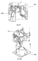
- FIG. 4 is an exploded view of electrical assembly 202 showing its constituent components according to an embodiment of the present invention.
- Electrical assembly 202 includes a single-piece insulator 404 that includes pre-defined features that facilitate attachment of other components of electrical assembly 202 . Insulator 404 is described in more detail below.
- Electrical assembly 202 may also include a primary PCB 402 having circuitry formed thereon.
- Primary PCB 402 may include multiple electronic components such as capacitors, resistors, transistors, etc. that are exposed to the incoming AC voltage, which is higher than the output DC voltage.
- Primary PCB 402 may be manufactured using any of the conventional techniques.
- Electrical assembly further includes a secondary PCB 406 that has circuitry thereon. The circuitry on secondary PCB may include filter circuit for smoothing out the DC voltage before being outputted.
- Secondary PCB 406 also includes connector 108 that can be used to output the DC voltage to external devices.
- FIG. 5 illustrates an isometric view of a single-piece insulator 404 according to an embodiment of the present invention.
- Insulator 404 can be prepared using a mold and filling the mold with glass-filled nylon to generate a single homogenous unit.
- insulator 404 has several features formed thereon. Each of these features serve a specific purpose.
- a recess 502 is designed to accommodate sections of a primary PCB (e.g., primary PCB 402 of FIG. 4 ).
- Opening 504 is designed to accommodate a transformer that is used to convert AC voltage to DC voltage.
- Recessed feature 506 is designed to accommodate a secondary PCB (e.g., PCB 406 of FIG. 4 ) and its associated connector (e.g., connector 108 of FIG.
- channels 508 are formed in the insulator walls. Channels 508 extend from a first surface of insulator 404 that receives the primary PCB to a second surface that receives the secondary PCB. Conductive members/pins 510 that are disposed in channels 508 provide electrical connectivity between the primary PCB and the secondary PCB. Pins 510 can be inserted into channels 508 within such that they extend slightly beyond each end of the channels. In some embodiments, conductive pins 510 may be manufactured using stainless steel as a core material, which would provide desired strength and stiffness. The core could be coated with a layer of copper to provide pins 510 with excellent conductivity properties.
- the layer of copper could be coated with a layer of nickel such that the pins should form excellent solder joints when soldered to other components or PCBs.
- the use of pins and channels simplifies the manufacturing process while improving overall reliability (due to the interconnections being physically fixed in place instead of being taped and/or glued in place).
- the use of pins and channels also reduces the overall space requirements for wiring, which is at a premium in a confined space such as within housing 102 .
- Insulator 404 may at the same time provide insulation and isolation between other sections of the two PCB's. In order to protect the low voltage sections of the adapter from the high voltage sections, it is beneficial to have an insulating material between the two voltage sections. If the power adapter is sufficiently large in dimension, air can be used as an effective insulator. However, in compact power adapter such as the one described herein, the various components of the adapter are packed densely leading to very little space between the low and high voltage components. In these circumstances, air is not an effective insulating medium and other insulating mechanisms may be needed.
- insulator 404 may be made from a material that is V-0 safety rated per the UL standards.
- insulator 404 may be made from glass-filled nylon. Other suitable materials such as silicone-based materials may also be used. Since the manufacturing process for the adapter includes several rounds to wave soldering, any material chose for insulator 404 needs to withstand wave soldering temperatures, which range from between 200° C. to 300° C.
- insulator 404 may have the following dimensions: a length in the range of about 20 mm to 22 mm, a width in the range of about 19 mm to 21 mm, and a height in the range of about 18 mm to 21 mm.
- an insulating tape can be used to cover the high voltage components; however such a manual technique is difficult to replicate with accuracy in a mass manufacturing environment. Also, allowing such an important step in the manufacturing process to be manual may expose the adapter to increased failure rates and more importantly is a significant safety hazard. A failure of the insulation may result in arcing or permanently damage the adapter and/or the external device connected to the adapter.
- the manufacturing process is greatly simplified and is more repeatable since the number of manual steps are significantly decreased or eliminated altogether.
- FIGS. 6A-6J illustrates steps in the assembly process of a power adapter according to an embodiment of the present invention.
- FIGS. 7A and 7B illustrate a corresponding flow diagram 700 for the assembly process depicted in FIGS. 6A-6J .
- the assembly process is described below with reference to FIGS. 6A-6J and 7A-7B .
- the entire assembly process may be automated or some parts of the assembly process may be manual while others may be automated.
- a different machine may be used to perform each step of the process or several steps in the process may be performed by a single machine.
- One skilled in the art will realize numerous variations in how the process is performed.
- a single-piece insulator structure 600 may be provided (Step 702 ).
- single-piece insulator structure 600 may be made using glass-filled nylon that is introduced into a custom mold.
- Single-piece insulator structure 600 includes many features formed thereon as described above.
- electrically conducting members 602 are inserted into the various channels that are formed in single-piece insulator structure 600 for that purpose (Step 704 ).
- Electrically conducting members may be made of any suitable conducting material such as copper clad steel, brass, aluminum, conductive metal alloys, etc. As described above, the electrically conducting members/pins provide an electrical path between the high-voltage circuitry and the low-voltage circuitry of the adapter.
- power transformer 604 is inserted in a recess of single-piece insulator structure 600 that is designed to accept the power transformer, as illustrated in FIG. 6B and Step 706 .
- an adhesive such as epoxy-based glue is applied around power transformer 604 and a compressive force is applied to the power transformer for a predetermined time in order to further ensure that the attachment of transformer 604 to single-piece insulator structure 600 is robust.
- a common mode choke 606 is attached to single-piece insulator structure 600 as illustrated in FIG. 6C (Step 708 ). Wires from common mode choke 606 are routed via designated channels 607 .
- pre-formed channels helps to keep the common mode choke wires in the right location (e.g., they remain tight and close to insulator structure 600 which makes installation of the completed subassembly in housing 102 significantly more efficient) and also increases overall manufacturing efficiency in that channels maintain the wires in the proper location for termination to other components downstream in the manufacturing process.
- a primary PCB 608 is attached to single-piece insulator structure 600 at a designated side as illustrated in FIG. 6D (Step 710 ).
- primary PCB 608 has high-voltage circuitry that interacts with the incoming AC voltage.
- an adhesive may be used to further make the attachment of primary PCB 608 to single-piece insulator 600 more robust.
- FIG. 6E illustrates assembly 610 that includes the single-piece insulator, the common mode choke, and the primary PCB attached together. Assembly 610 is shown flipped over to reveal the region of single-piece insulator that can accept the secondary PCB.
- insulator structure 600 in the process greatly increases the likelihood that the manufacturing process has been accomplished without error.
- a wave solder process can be used to solder the pins, capacitors and other components to primary PCB 608 , at which point the subassembly is substantially complete.
- Secondary PCB includes low-voltage circuitry and connector 108 , which is described above.
- the low voltage circuitry may include, e.g., filter circuitry to smooth out the DC output voltage before it is provided to a connected external device.
- FIG. 6G shows a completely electrical assembly 614 . Assembly 614 is similar to assembly 202 illustrated in FIG. 2 . Another wave soldering process can be utilized to secure and electrically couple connector 108 (and any additional discrete components needs (not shown)) to secondary PCB 612 , as well as securing and electrically coupling the appropriate pins to secondary PCB 612 .
- Step 714 the inputs to the primary stage of the transformer of assembly 614 are connected to input terminals 616 of cap assembly 104 (Step 714 ) which provides the capability for wall power to be coupled to the primary stage of the transformer when the completed power adapter is plugged into a wall outlet, as illustrated in FIG. 6H .
- the entire assembly 614 is inserted into adapter housing 102 (Step 716 ), as illustrated in FIG. 6I .
- cap assembly 104 is welded to housing 102 using ultrasonic welding (Step 718 ).
- power adapter 100 is complete as illustrated in FIG. 6J .
- FIGS. 6A-6J and 7A-7B provide a particular method of manufacturing a power adapter according to an embodiment of the present invention. Other sequences of steps may also be performed according to alternative embodiments. For example, alternative embodiments of the present invention may perform the steps outlined above in a different order. Moreover, the individual steps illustrated in FIGS. 6A-6J and 7A-7B may include multiple sub-steps that may be performed in various sequences as appropriate to the individual step. Furthermore, additional steps may be added or removed depending on the particular applications. One of ordinary skill in the art would recognize many variations, modifications, and alternatives.
Landscapes
- Engineering & Computer Science (AREA)
- Microelectronics & Electronic Packaging (AREA)
- Power Engineering (AREA)
- Connector Housings Or Holding Contact Members (AREA)
- Rectifiers (AREA)
- Dc-Dc Converters (AREA)
Abstract
Description
Claims (20)
Priority Applications (1)
| Application Number | Priority Date | Filing Date | Title |
|---|---|---|---|
| US15/156,629 US9728906B2 (en) | 2011-10-13 | 2016-05-17 | Power adapter with a single-piece insulator assembly |
Applications Claiming Priority (4)
| Application Number | Priority Date | Filing Date | Title |
|---|---|---|---|
| US201161547020P | 2011-10-13 | 2011-10-13 | |
| PCT/US2012/059798 WO2013055948A2 (en) | 2011-10-13 | 2012-10-11 | Power adapter with a single-piece insulator assembly |
| US201414351287A | 2014-04-11 | 2014-04-11 | |
| US15/156,629 US9728906B2 (en) | 2011-10-13 | 2016-05-17 | Power adapter with a single-piece insulator assembly |
Related Parent Applications (2)
| Application Number | Title | Priority Date | Filing Date |
|---|---|---|---|
| PCT/US2012/059798 Continuation WO2013055948A2 (en) | 2011-10-13 | 2012-10-11 | Power adapter with a single-piece insulator assembly |
| US14/351,287 Continuation US9343850B2 (en) | 2011-10-13 | 2012-11-10 | Power adapter with a single-piece insulator assembly |
Publications (2)
| Publication Number | Publication Date |
|---|---|
| US20160276783A1 US20160276783A1 (en) | 2016-09-22 |
| US9728906B2 true US9728906B2 (en) | 2017-08-08 |
Family
ID=47190130
Family Applications (2)
| Application Number | Title | Priority Date | Filing Date |
|---|---|---|---|
| US14/351,287 Active 2032-11-06 US9343850B2 (en) | 2011-10-13 | 2012-11-10 | Power adapter with a single-piece insulator assembly |
| US15/156,629 Expired - Fee Related US9728906B2 (en) | 2011-10-13 | 2016-05-17 | Power adapter with a single-piece insulator assembly |
Family Applications Before (1)
| Application Number | Title | Priority Date | Filing Date |
|---|---|---|---|
| US14/351,287 Active 2032-11-06 US9343850B2 (en) | 2011-10-13 | 2012-11-10 | Power adapter with a single-piece insulator assembly |
Country Status (6)
| Country | Link |
|---|---|
| US (2) | US9343850B2 (en) |
| EP (2) | EP2766960B1 (en) |
| KR (1) | KR20140075001A (en) |
| CN (2) | CN103959574B (en) |
| TW (1) | TWI495233B (en) |
| WO (1) | WO2013055948A2 (en) |
Cited By (3)
| Publication number | Priority date | Publication date | Assignee | Title |
|---|---|---|---|---|
| US20220416490A1 (en) * | 2020-03-18 | 2022-12-29 | Guangdong Gopod Group Holding Co., Ltd. | Power adapter |
| US11605925B2 (en) | 2020-03-18 | 2023-03-14 | Guangdong Gopod Group Holding Co., Ltd. | Power adapter |
| US20240204395A1 (en) * | 2021-07-13 | 2024-06-20 | Honor Device Co., Ltd. | Elastic piece connection structure and electronic device |
Families Citing this family (77)
| Publication number | Priority date | Publication date | Assignee | Title |
|---|---|---|---|---|
| EP2766960B1 (en) | 2011-10-13 | 2020-07-01 | Apple Inc. | Insulator assembly for power adapter, power adapter and method for assembling a power adapter |
| TW201423355A (en) * | 2012-12-03 | 2014-06-16 | Hon Hai Prec Ind Co Ltd | Power supply module |
| US20150064970A1 (en) * | 2013-09-04 | 2015-03-05 | Qualcomm Incorporated | Systems, apparatus, and methods for an embedded emissions filter circuit in a power cable |
| US9362765B1 (en) * | 2013-11-08 | 2016-06-07 | Amazon Technologies, Inc. | Systems and methods for a power adapter for mobile devices |
| CN204361885U (en) * | 2015-01-05 | 2015-05-27 | 富士康(昆山)电脑接插件有限公司 | Power supply adaptor |
| CN106208174B (en) * | 2015-05-07 | 2025-05-27 | 上海飞科电器股份有限公司 | Waterproof power adapter with USB port |
| CN106469973B (en) * | 2015-08-10 | 2019-04-02 | 全汉企业股份有限公司 | Adapter power supply |
| US10256583B2 (en) * | 2015-08-10 | 2019-04-09 | Fsp Technology Inc. | Power adapter |
| US9356380B1 (en) * | 2015-08-20 | 2016-05-31 | Stuff Electronics (Dongguan) Limited | Power adaptor |
| US9680249B2 (en) * | 2015-09-30 | 2017-06-13 | Apple Inc. | Molded enclosures having a seamless appearance |
| TWM544183U (en) * | 2015-09-30 | 2017-06-21 | 蘋果公司 | Enclosures having a seamless appearance |
| USD778825S1 (en) * | 2016-01-05 | 2017-02-14 | Battery-Biz, Inc. | Portable charger |
| USD778823S1 (en) * | 2016-01-05 | 2017-02-14 | Battery-Biz, Inc. | Portable charger |
| USD778824S1 (en) * | 2016-01-05 | 2017-02-14 | Battery-Biz, Inc. | Portable charger |
| USD778826S1 (en) * | 2016-01-05 | 2017-02-14 | Battery-Biz, Inc. | Portable charger |
| EP3258547A1 (en) * | 2016-06-17 | 2017-12-20 | Tyco Electronics Componentes Electromecanicos Lda | Electric automotive connector with increased mounting surface |
| USD790465S1 (en) * | 2016-06-20 | 2017-06-27 | Dongguan Zhaoshun Electronics Technology Co., Ltd | Power adapter |
| CN107645231B (en) | 2016-07-20 | 2019-10-11 | 光宝电子(广州)有限公司 | Power adapter |
| CA172904S (en) * | 2016-08-04 | 2017-11-10 | Norman R Byrne | Electrical power unit |
| CN106229733A (en) * | 2016-09-29 | 2016-12-14 | 赫霍艾迪欧洲公司 | Safety power socket for children adapter |
| TWI654512B (en) | 2016-10-06 | 2019-03-21 | 綠點高新科技股份有限公司 | Power adapter device and manufacturing method thereof |
| CN106602342B (en) * | 2017-01-09 | 2019-01-01 | 广州华凌制冷设备有限公司 | socket and preparation method thereof |
| US12027968B2 (en) | 2017-04-01 | 2024-07-02 | John J. King | Power adapters and methods of implementing a power adapter |
| US12093004B1 (en) | 2017-04-01 | 2024-09-17 | Smart Power Partners LLC | In-wall power adapter and method of implementing an in-wall power adapter |
| US10996645B1 (en) | 2017-04-01 | 2021-05-04 | Smart Power Partners LLC | Modular power adapters and methods of implementing modular power adapters |
| US10727731B1 (en) | 2017-04-01 | 2020-07-28 | Smart Power Partners, LLC | Power adapters adapted to receive a module and methods of implementing power adapters with modules |
| US10530597B1 (en) | 2017-04-01 | 2020-01-07 | Smart Power Partners LLC | System for controlling a plurality of power switches configured to apply power to devices |
| USD819566S1 (en) * | 2017-06-23 | 2018-06-05 | Delta Electronics, Inc. | Power adapter |
| TWI638511B (en) * | 2017-07-11 | 2018-10-11 | 綠點高新科技股份有限公司 | Power converter |
| USD841582S1 (en) * | 2017-10-11 | 2019-02-26 | Shenzhen TXRICH technology Co., LTD | Charger |
| USD879720S1 (en) * | 2017-12-05 | 2020-03-31 | Ningbo Gongniu Digital Technology Co., Ltd | Electric socket |
| USD867989S1 (en) | 2018-05-16 | 2019-11-26 | Apple Inc. | Adapter |
| USD867285S1 (en) * | 2018-05-16 | 2019-11-19 | Apple Inc. | Adapter |
| CN110553676B (en) * | 2018-05-30 | 2022-02-01 | 南昌欧菲显示科技有限公司 | sensor |
| US10622752B2 (en) | 2018-05-31 | 2020-04-14 | Apple Inc. | Ultrasonic weld joint with integral flash trap |
| US10505308B1 (en) * | 2018-05-31 | 2019-12-10 | Apple Inc. | Dual cup enclosure for electronic devices |
| USD864871S1 (en) * | 2018-06-07 | 2019-10-29 | Lingan Intelligent Technology Co., Ltd | Socket |
| USD867286S1 (en) | 2018-06-07 | 2019-11-19 | Apple Inc. | Adapter |
| USD874400S1 (en) | 2018-06-07 | 2020-02-04 | Apple Inc. | Adapter |
| USD867287S1 (en) | 2018-06-07 | 2019-11-19 | Apple Inc. | Adapter |
| FR3082369B1 (en) * | 2018-06-08 | 2021-02-19 | Valeo Equip Electr Moteur | ELECTRICAL CIRCUIT, SWITCHING ARM AND VOLTAGE CONVERTER |
| DE202018106353U1 (en) * | 2018-11-08 | 2020-02-11 | Woco Industrietechnik Gmbh | Plug adapter for docking to a solenoid valve |
| USD858439S1 (en) * | 2019-05-09 | 2019-09-03 | Shenzhen Hai Run Tian Heng Technology Co., Ltd. | Charging socket |
| US12045071B1 (en) | 2019-06-30 | 2024-07-23 | Smart Power Partners LLC | In-wall power adapter having an outlet |
| US11579640B1 (en) | 2019-06-30 | 2023-02-14 | Smart Power Partners LLC | Control attachment for an in-wall power adapter |
| US10958020B1 (en) | 2019-06-30 | 2021-03-23 | Smart Power Partners LLC | Control attachment for an in-wall power adapter and method of controlling an in-wall power adapter |
| US11231730B1 (en) | 2019-06-30 | 2022-01-25 | Smart Power Power LLC | Control attachment for a power adapter configured to control power applied to a load |
| US11189948B1 (en) | 2019-06-30 | 2021-11-30 | Smart Power Partners LLC | Power adapter and method of implementing a power adapter to provide power to a load |
| US11201444B1 (en) | 2019-06-30 | 2021-12-14 | Smart Power Partners LLC | Power adapter having contact elements in a recess and method of controlling a power adapter |
| US12066848B1 (en) | 2019-06-30 | 2024-08-20 | Smart Power Partners LLC | In-wall power adaper adapted to receive a control attachment and method of implementing a power adapter |
| US10958026B1 (en) | 2019-06-30 | 2021-03-23 | Smart Power Partners LLC | Contactless thermometer for an in-wall power adapter |
| US11460874B1 (en) | 2019-06-30 | 2022-10-04 | Smart Power Partners LLC | In-wall power adapter configured to control the application of power to a load |
| US10917956B1 (en) | 2019-06-30 | 2021-02-09 | Smart Power Partners LLC | Control attachment configured to provide power to a load and method of configuring a control attachment |
| US11599177B1 (en) | 2019-06-30 | 2023-03-07 | Smart Power Partners LLC | Power adapter arrangement having a power adapter and a control attachment |
| US11264769B1 (en) | 2019-06-30 | 2022-03-01 | Smart Power Partners LLC | Power adapter having contact elements in a recess and method of controlling a power adapter |
| US11043768B1 (en) | 2019-06-30 | 2021-06-22 | Smart Power Partners LLC | Power adapter configured to provide power to a load and method of implementing a power adapter |
| US10938168B2 (en) | 2019-06-30 | 2021-03-02 | Smart Power Partners LLC | In-wall power adapter and method of controlling the application of power to a load |
| US10965068B1 (en) | 2019-06-30 | 2021-03-30 | Smart Power Partners LLC | In-wall power adapter having an outlet and method of controlling an in-wall power adapter |
| US12164350B1 (en) | 2019-06-30 | 2024-12-10 | Smart Power Partners LLC | Power adapter configured to provide power to a load |
| CN112366481A (en) * | 2019-07-25 | 2021-02-12 | 富士康(昆山)电脑接插件有限公司 | Electric connector combination, plug connector and socket connector |
| USD879711S1 (en) * | 2019-10-22 | 2020-03-31 | Huang Ruiwu | USB plug |
| USD879712S1 (en) * | 2019-11-22 | 2020-03-31 | Shenzhen Shibituo Technology Co., Ltd. | Battery charger |
| USD879044S1 (en) * | 2019-11-22 | 2020-03-24 | Shenzhen Shibituo Technology Co., Ltd. | Battery adapter |
| USD941766S1 (en) * | 2020-03-09 | 2022-01-25 | Guangdong Gopod Group Holding Co., Ltd. | Power adapter |
| JP1671480S (en) * | 2020-03-09 | 2020-11-02 | ||
| US11515679B2 (en) * | 2020-06-24 | 2022-11-29 | Apple Inc. | Power adapter for electronic devices |
| USD942939S1 (en) * | 2020-09-07 | 2022-02-08 | Babyliss FACO SRL | Charger |
| USD942938S1 (en) * | 2020-09-07 | 2022-02-08 | Babyliss FACO SRL | Charger |
| US12300948B2 (en) | 2021-11-03 | 2025-05-13 | Smart Power Partners LLC | Control module having a control circuit and adapted to be attached to a power adapter |
| USD1008973S1 (en) * | 2021-12-08 | 2023-12-26 | Xianpo Chen | Outlet converter |
| CN114552944B (en) * | 2022-01-29 | 2026-03-17 | 华为数字能源技术有限公司 | power adapter |
| KR102529189B1 (en) * | 2022-11-15 | 2023-05-04 | 정지민 | Space saving multi outlet |
| KR102751006B1 (en) * | 2023-03-08 | 2025-01-06 | 엘지전자 주식회사 | Display device |
| USD1007430S1 (en) * | 2023-08-10 | 2023-12-12 | Shenzhen Early Century Technology Co., Ltd. | Charging adapter |
| USD1008189S1 (en) * | 2023-09-27 | 2023-12-19 | Shenzhen Shi C&C Technology Co., LTD | Electric plug |
| USD1008190S1 (en) * | 2023-09-27 | 2023-12-19 | Shenzhen Shi C&C Technology Co., LTD | Electric plug |
| USD1074589S1 (en) * | 2024-07-15 | 2025-05-13 | Guilin Cao | Charger |
Citations (25)
| Publication number | Priority date | Publication date | Assignee | Title |
|---|---|---|---|---|
| US3930707A (en) | 1974-06-10 | 1976-01-06 | A P Products Incorporated | Interface connector |
| US4156219A (en) | 1976-01-12 | 1979-05-22 | Ottermill Limited | Electric circuit breaker |
| US5403208A (en) | 1989-01-19 | 1995-04-04 | Burndy Corporation | Extended card edge connector and socket |
| WO2001008262A2 (en) | 1999-07-23 | 2001-02-01 | Walter Roland Chen | Ac/dc adapter 110/230 volts, with multiple dc outputs |
| US20030082952A1 (en) | 2000-10-24 | 2003-05-01 | Bel-Fuse, Inc. | Split-package AC adapter |
| US20050266730A1 (en) | 1994-04-26 | 2005-12-01 | Comarco Wireless Technologies, Inc. | Programmable power supply |
| US7121847B1 (en) | 2005-02-24 | 2006-10-17 | Yazaki North America, Inc. | Flame-retardant cap for a high current connection |
| US20080315831A1 (en) | 2007-06-20 | 2008-12-25 | Li Peter T | Ac-to-dc adapter for mobile system |
| US20080315931A1 (en) | 2007-06-20 | 2008-12-25 | Kawasaki Microelectronics, Inc. | Semiconductor integrated circuit having active and sleep modes and non-retention flip-flop that is initialized when switching from sleep mode to active mode |
| TW200903962A (en) | 2007-07-13 | 2009-01-16 | Hon Hai Prec Ind Co Ltd | Multiple output AC/DC power adapter |
| US20090093149A1 (en) | 2007-10-09 | 2009-04-09 | Anderson Power Products, Inc. | Electrical connector system with two part housing |
| CN101552541A (en) | 2008-12-08 | 2009-10-07 | 厦门大学 | Universal power adapter |
| CN101552514A (en) | 2009-05-14 | 2009-10-07 | 永济新时速电机电器有限责任公司 | High-rotating-speed pulling motor |
| CN101901998A (en) | 2009-05-26 | 2010-12-01 | 富士康(昆山)电脑接插件有限公司 | Electric connector |
| TWM404542U (en) | 2010-12-08 | 2011-05-21 | Darfon Electronics Corp | Power adapter |
| US7978489B1 (en) | 2007-08-03 | 2011-07-12 | Flextronics Ap, Llc | Integrated power converters |
| US8011975B1 (en) | 2010-05-27 | 2011-09-06 | Apple Inc. | Power connector having protective interior cover |
| US8021183B2 (en) * | 2008-10-31 | 2011-09-20 | Apple Inc. | Cold headed electric plug arm |
| US20120155041A1 (en) * | 2008-12-23 | 2012-06-21 | Wey-Jiun Lin | Compact device housing and assembly techniques therefor |
| US20120169272A1 (en) * | 2011-01-03 | 2012-07-05 | David Khalepari | Portable usb mini-charger device |
| WO2013055948A2 (en) | 2011-10-13 | 2013-04-18 | Apple Inc. | Power adapter with a single-piece insulator assembly |
| US8460017B1 (en) * | 2009-01-26 | 2013-06-11 | Amazon Technologies, Inc. | Electrical power adapter |
| US20130300366A1 (en) * | 2012-03-23 | 2013-11-14 | Cheng Uei Precision Industry Co., Ltd. | Charger |
| US8597049B2 (en) | 2011-07-19 | 2013-12-03 | Cooper Technologies Company | Modular open fuse holder |
| US8790124B2 (en) * | 2012-06-01 | 2014-07-29 | Lite-On Electronics (Guangzhou) Limited | Electrical plug device and electronic apparatus including the same |
-
2012
- 2012-10-11 EP EP12787558.1A patent/EP2766960B1/en active Active
- 2012-10-11 CN CN201280049938.1A patent/CN103959574B/en active Active
- 2012-10-11 KR KR1020147012530A patent/KR20140075001A/en not_active Ceased
- 2012-10-11 EP EP20183147.6A patent/EP3790124A1/en not_active Withdrawn
- 2012-10-11 WO PCT/US2012/059798 patent/WO2013055948A2/en not_active Ceased
- 2012-10-11 CN CN201610509487.5A patent/CN105914537B/en not_active Expired - Fee Related
- 2012-10-12 TW TW101137816A patent/TWI495233B/en active
- 2012-11-10 US US14/351,287 patent/US9343850B2/en active Active
-
2016
- 2016-05-17 US US15/156,629 patent/US9728906B2/en not_active Expired - Fee Related
Patent Citations (32)
| Publication number | Priority date | Publication date | Assignee | Title |
|---|---|---|---|---|
| US3930707A (en) | 1974-06-10 | 1976-01-06 | A P Products Incorporated | Interface connector |
| US4156219A (en) | 1976-01-12 | 1979-05-22 | Ottermill Limited | Electric circuit breaker |
| US5403208A (en) | 1989-01-19 | 1995-04-04 | Burndy Corporation | Extended card edge connector and socket |
| US20050266730A1 (en) | 1994-04-26 | 2005-12-01 | Comarco Wireless Technologies, Inc. | Programmable power supply |
| WO2001008262A2 (en) | 1999-07-23 | 2001-02-01 | Walter Roland Chen | Ac/dc adapter 110/230 volts, with multiple dc outputs |
| US20030082952A1 (en) | 2000-10-24 | 2003-05-01 | Bel-Fuse, Inc. | Split-package AC adapter |
| US7121847B1 (en) | 2005-02-24 | 2006-10-17 | Yazaki North America, Inc. | Flame-retardant cap for a high current connection |
| US20080315831A1 (en) | 2007-06-20 | 2008-12-25 | Li Peter T | Ac-to-dc adapter for mobile system |
| US20080315931A1 (en) | 2007-06-20 | 2008-12-25 | Kawasaki Microelectronics, Inc. | Semiconductor integrated circuit having active and sleep modes and non-retention flip-flop that is initialized when switching from sleep mode to active mode |
| TWI345358B (en) | 2007-07-13 | 2011-07-11 | Hon Hai Prec Ind Co Ltd | Multiple output ac/dc power adapter |
| TW200903962A (en) | 2007-07-13 | 2009-01-16 | Hon Hai Prec Ind Co Ltd | Multiple output AC/DC power adapter |
| US7978489B1 (en) | 2007-08-03 | 2011-07-12 | Flextronics Ap, Llc | Integrated power converters |
| US20090093149A1 (en) | 2007-10-09 | 2009-04-09 | Anderson Power Products, Inc. | Electrical connector system with two part housing |
| US8021183B2 (en) * | 2008-10-31 | 2011-09-20 | Apple Inc. | Cold headed electric plug arm |
| CN101552541A (en) | 2008-12-08 | 2009-10-07 | 厦门大学 | Universal power adapter |
| US20120155041A1 (en) * | 2008-12-23 | 2012-06-21 | Wey-Jiun Lin | Compact device housing and assembly techniques therefor |
| US8460017B1 (en) * | 2009-01-26 | 2013-06-11 | Amazon Technologies, Inc. | Electrical power adapter |
| CN101552514A (en) | 2009-05-14 | 2009-10-07 | 永济新时速电机电器有限责任公司 | High-rotating-speed pulling motor |
| CN101901998A (en) | 2009-05-26 | 2010-12-01 | 富士康(昆山)电脑接插件有限公司 | Electric connector |
| US8011975B1 (en) | 2010-05-27 | 2011-09-06 | Apple Inc. | Power connector having protective interior cover |
| US20110300754A1 (en) * | 2010-05-27 | 2011-12-08 | Apple Inc. | Power connector having protective interior cover |
| TWM404542U (en) | 2010-12-08 | 2011-05-21 | Darfon Electronics Corp | Power adapter |
| US20120169272A1 (en) * | 2011-01-03 | 2012-07-05 | David Khalepari | Portable usb mini-charger device |
| US8597049B2 (en) | 2011-07-19 | 2013-12-03 | Cooper Technologies Company | Modular open fuse holder |
| WO2013055948A2 (en) | 2011-10-13 | 2013-04-18 | Apple Inc. | Power adapter with a single-piece insulator assembly |
| TW201330467A (en) | 2011-10-13 | 2013-07-16 | Apple Inc | Power adapter with a single-piece insulator assembly |
| CN103959574A (en) | 2011-10-13 | 2014-07-30 | 苹果公司 | Power Adapter with One-Piece Insulator Assembly |
| US20140308853A1 (en) | 2011-10-13 | 2014-10-16 | Apple Inc. | Power adapter with a single-piece insulator assembly |
| CN105914537A (en) | 2011-10-13 | 2016-08-31 | 苹果公司 | Power adapter with a single-piece insulator assembly |
| US20160276783A1 (en) | 2011-10-13 | 2016-09-22 | Apple Inc. | Power adapter with a single-piece insulator assembly |
| US20130300366A1 (en) * | 2012-03-23 | 2013-11-14 | Cheng Uei Precision Industry Co., Ltd. | Charger |
| US8790124B2 (en) * | 2012-06-01 | 2014-07-29 | Lite-On Electronics (Guangzhou) Limited | Electrical plug device and electronic apparatus including the same |
Non-Patent Citations (14)
| Title |
|---|
| International Preliminary Report on Patentability for International PCT Application No. PCT/US2012/059798, mailed Apr. 24, 2014, 8 pages. |
| International Search Report and Written Opinion for International PCT Application No. PCT/US2012/059798, mailed Apr. 9, 2013, 13 pages. |
| Musavi et al., "Energy Efficiency in Plug-in Hybrid Electric Vehicle Chargers: Evaluation and Comparison of Front End AC-DC Topologies", Energy Conversion Congress and Exposition (ECCE), IEEE, Sep. 2011, pp. 273-280. |
| Non-Final Office Action for U.S. Appl. No. 14/351,287, mailed Sep. 16, 2015, 20 pages. |
| Notice of Allowance for Taiwanese Patent Application No. 101137816, mailed May 26, 2015, 3 pages. |
| Notice of Allowance for U.S. Appl. No. 14/351,287, mailed Feb. 17, 2016, 8 pages. |
| Office Action for Chinese Patent Application No. 201280049938.1, mailed Apr. 22, 2016, 7 pages. |
| Office Action for Chinese Patent Application No. 201280049938.1, mailed Aug. 19, 2015, 18 pages. |
| Office Action for Chinese Patent Application No. 201280049938.1, mailed Oct. 8, 2016, 6 pages. |
| Office Action for European Patent Application No. 12787558.1, mailed Feb. 15, 2016, 5 pages. |
| Office Action for European Patent Application No. 12787558.1, mailed Jan. 21, 2015, 3 pages. |
| Office Action for European Patent Application No. 12787558.1, mailed Jul. 21, 2015, 3 pages. |
| Office Action for European Patent Application No. 12787558.1, mailed May 21, 2014, 2 pages. |
| Office Action for Taiwanese Patent Application No. 101137816, mailed Jun. 23, 2014, 21 pages. |
Cited By (5)
| Publication number | Priority date | Publication date | Assignee | Title |
|---|---|---|---|---|
| US20220416490A1 (en) * | 2020-03-18 | 2022-12-29 | Guangdong Gopod Group Holding Co., Ltd. | Power adapter |
| US11605925B2 (en) | 2020-03-18 | 2023-03-14 | Guangdong Gopod Group Holding Co., Ltd. | Power adapter |
| US11757241B2 (en) * | 2020-03-18 | 2023-09-12 | Guangdong Gopod Group Holding Co., Ltd. | Power adapter with protective shield |
| US20240204395A1 (en) * | 2021-07-13 | 2024-06-20 | Honor Device Co., Ltd. | Elastic piece connection structure and electronic device |
| US12519220B2 (en) * | 2021-07-13 | 2026-01-06 | Honor Device Co., Ltd. | Elastic piece connection structure and electronic device |
Also Published As
| Publication number | Publication date |
|---|---|
| US20160276783A1 (en) | 2016-09-22 |
| US9343850B2 (en) | 2016-05-17 |
| CN105914537A (en) | 2016-08-31 |
| CN103959574A (en) | 2014-07-30 |
| TW201330467A (en) | 2013-07-16 |
| TWI495233B (en) | 2015-08-01 |
| WO2013055948A3 (en) | 2013-07-04 |
| CN103959574B (en) | 2017-04-05 |
| EP2766960B1 (en) | 2020-07-01 |
| US20140308853A1 (en) | 2014-10-16 |
| CN105914537B (en) | 2018-04-13 |
| KR20140075001A (en) | 2014-06-18 |
| EP3790124A1 (en) | 2021-03-10 |
| WO2013055948A2 (en) | 2013-04-18 |
| EP2766960A2 (en) | 2014-08-20 |
Similar Documents
| Publication | Publication Date | Title |
|---|---|---|
| US9728906B2 (en) | Power adapter with a single-piece insulator assembly | |
| US8743556B2 (en) | Printed circuit board connection assembly | |
| CN101443966B (en) | Modular electronic header assembly and methods of manufacture | |
| JP5990376B2 (en) | Power supply unit partially filled with compound and manufacturing method thereof | |
| US9486956B2 (en) | Power adapter components, housing and methods of assembly | |
| US11855373B2 (en) | Connector assembly with a detection system | |
| US8888509B2 (en) | Electrical connector and method of assembling same | |
| CN107808756A (en) | A kind of flat-plate transformer and switch power source adapter | |
| CN101908683B (en) | Electric connector and assembly method thereof | |
| CN106953200A (en) | Electronic card supports, assemblies, voltage converters and motors | |
| CN113162295B (en) | DC brush motor | |
| US20110122589A1 (en) | Magnetic element having improved transformers and commom mode chokes | |
| US11165178B2 (en) | Electrical interconnection system and method for electrically interconnecting electrical components of a module | |
| CN217848536U (en) | High-reliability filtering electric connector for socket or plug | |
| CN215989578U (en) | USB interface and electronic equipment | |
| CN212062873U (en) | electrical connector | |
| CN201311976Y (en) | Improved wire conductor clamping structure of control box with circuit | |
| CN221614318U (en) | Circuit board, power module and power system | |
| CN100530847C (en) | Plug-in power pack | |
| CN120895808B (en) | Button cell and electronic equipment | |
| CN211320522U (en) | Transmission connector and transmission cable | |
| CN210535907U (en) | USB A male plug and data line with same | |
| CN115693320A (en) | Connection structure between members | |
| CN116646755A (en) | High voltage connector and high voltage distribution box | |
| CN102801025A (en) | Electric connector |
Legal Events
| Date | Code | Title | Description |
|---|---|---|---|
| FEPP | Fee payment procedure |
Free format text: PAYER NUMBER DE-ASSIGNED (ORIGINAL EVENT CODE: RMPN); ENTITY STATUS OF PATENT OWNER: LARGE ENTITY Free format text: PAYOR NUMBER ASSIGNED (ORIGINAL EVENT CODE: ASPN); ENTITY STATUS OF PATENT OWNER: LARGE ENTITY |
|
| STCF | Information on status: patent grant |
Free format text: PATENTED CASE |
|
| MAFP | Maintenance fee payment |
Free format text: PAYMENT OF MAINTENANCE FEE, 4TH YEAR, LARGE ENTITY (ORIGINAL EVENT CODE: M1551); ENTITY STATUS OF PATENT OWNER: LARGE ENTITY Year of fee payment: 4 |
|
| FEPP | Fee payment procedure |
Free format text: MAINTENANCE FEE REMINDER MAILED (ORIGINAL EVENT CODE: REM.); ENTITY STATUS OF PATENT OWNER: LARGE ENTITY |
|
| LAPS | Lapse for failure to pay maintenance fees |
Free format text: PATENT EXPIRED FOR FAILURE TO PAY MAINTENANCE FEES (ORIGINAL EVENT CODE: EXP.); ENTITY STATUS OF PATENT OWNER: LARGE ENTITY |
|
| STCH | Information on status: patent discontinuation |
Free format text: PATENT EXPIRED DUE TO NONPAYMENT OF MAINTENANCE FEES UNDER 37 CFR 1.362 |
|
| FP | Lapsed due to failure to pay maintenance fee |
Effective date: 20250808 |