US9720299B1 - Electrochromic multi-layer devices with cross-linked ion conducting polymer - Google Patents
Electrochromic multi-layer devices with cross-linked ion conducting polymer Download PDFInfo
- Publication number
- US9720299B1 US9720299B1 US14/994,090 US201614994090A US9720299B1 US 9720299 B1 US9720299 B1 US 9720299B1 US 201614994090 A US201614994090 A US 201614994090A US 9720299 B1 US9720299 B1 US 9720299B1
- Authority
- US
- United States
- Prior art keywords
- ion conducting
- conducting polymer
- layer
- electrochromic
- cross
- Prior art date
- Legal status (The legal status is an assumption and is not a legal conclusion. Google has not performed a legal analysis and makes no representation as to the accuracy of the status listed.)
- Active - Reinstated
Links
- 239000002322 conducting polymer Substances 0.000 title claims abstract description 72
- 229920001940 conductive polymer Polymers 0.000 title claims abstract description 72
- 150000002500 ions Chemical class 0.000 claims abstract description 128
- 238000000034 method Methods 0.000 claims abstract description 25
- 229910001416 lithium ion Inorganic materials 0.000 claims abstract description 24
- 229910052744 lithium Inorganic materials 0.000 claims abstract description 19
- WHXSMMKQMYFTQS-UHFFFAOYSA-N Lithium Chemical compound [Li] WHXSMMKQMYFTQS-UHFFFAOYSA-N 0.000 claims abstract description 18
- 230000008569 process Effects 0.000 claims abstract description 18
- HBBGRARXTFLTSG-UHFFFAOYSA-N Lithium ion Chemical compound [Li+] HBBGRARXTFLTSG-UHFFFAOYSA-N 0.000 claims abstract description 17
- 239000000758 substrate Substances 0.000 claims description 53
- 239000011521 glass Substances 0.000 claims description 20
- 238000004132 cross linking Methods 0.000 claims description 17
- 238000000151 deposition Methods 0.000 claims description 5
- 238000004519 manufacturing process Methods 0.000 claims description 5
- 230000009477 glass transition Effects 0.000 claims description 4
- 238000010030 laminating Methods 0.000 claims description 3
- 230000001678 irradiating effect Effects 0.000 claims description 2
- 239000000853 adhesive Substances 0.000 abstract description 5
- 230000001070 adhesive effect Effects 0.000 abstract description 5
- 239000000463 material Substances 0.000 description 59
- 239000000178 monomer Substances 0.000 description 45
- 239000000203 mixture Substances 0.000 description 41
- 239000010416 ion conductor Substances 0.000 description 37
- 230000003287 optical effect Effects 0.000 description 24
- 230000008859 change Effects 0.000 description 22
- -1 oligomer Substances 0.000 description 22
- 238000009472 formulation Methods 0.000 description 17
- 230000005670 electromagnetic radiation Effects 0.000 description 15
- 239000003795 chemical substances by application Substances 0.000 description 13
- PXHVJJICTQNCMI-UHFFFAOYSA-N Nickel Chemical compound [Ni] PXHVJJICTQNCMI-UHFFFAOYSA-N 0.000 description 12
- 239000004014 plasticizer Substances 0.000 description 12
- 229920000642 polymer Polymers 0.000 description 12
- 239000003054 catalyst Substances 0.000 description 11
- 229910052751 metal Inorganic materials 0.000 description 11
- 239000002184 metal Substances 0.000 description 11
- 239000007787 solid Substances 0.000 description 11
- 239000010408 film Substances 0.000 description 10
- 238000000576 coating method Methods 0.000 description 9
- 239000004020 conductor Substances 0.000 description 9
- HXJUTPCZVOIRIF-UHFFFAOYSA-N sulfolane Chemical compound O=S1(=O)CCCC1 HXJUTPCZVOIRIF-UHFFFAOYSA-N 0.000 description 9
- 230000007704 transition Effects 0.000 description 9
- XLOMVQKBTHCTTD-UHFFFAOYSA-N Zinc monoxide Chemical compound [Zn]=O XLOMVQKBTHCTTD-UHFFFAOYSA-N 0.000 description 8
- AMWRITDGCCNYAT-UHFFFAOYSA-L hydroxy(oxo)manganese;manganese Chemical compound [Mn].O[Mn]=O.O[Mn]=O AMWRITDGCCNYAT-UHFFFAOYSA-L 0.000 description 8
- 229910044991 metal oxide Inorganic materials 0.000 description 8
- 150000004706 metal oxides Chemical class 0.000 description 8
- 238000004040 coloring Methods 0.000 description 7
- 229920003023 plastic Polymers 0.000 description 7
- 239000004033 plastic Substances 0.000 description 7
- 229910052721 tungsten Inorganic materials 0.000 description 7
- 229910001930 tungsten oxide Inorganic materials 0.000 description 7
- VYPSYNLAJGMNEJ-UHFFFAOYSA-N Silicium dioxide Chemical compound O=[Si]=O VYPSYNLAJGMNEJ-UHFFFAOYSA-N 0.000 description 6
- 239000002800 charge carrier Substances 0.000 description 6
- 239000002131 composite material Substances 0.000 description 6
- 125000001183 hydrocarbyl group Chemical group 0.000 description 6
- 239000007788 liquid Substances 0.000 description 6
- 229910052759 nickel Inorganic materials 0.000 description 6
- USPVIMZDBBWXGM-UHFFFAOYSA-N nickel;oxotungsten Chemical compound [Ni].[W]=O USPVIMZDBBWXGM-UHFFFAOYSA-N 0.000 description 6
- QGLKJKCYBOYXKC-UHFFFAOYSA-N nonaoxidotritungsten Chemical compound O=[W]1(=O)O[W](=O)(=O)O[W](=O)(=O)O1 QGLKJKCYBOYXKC-UHFFFAOYSA-N 0.000 description 6
- 238000006116 polymerization reaction Methods 0.000 description 6
- 239000010409 thin film Substances 0.000 description 6
- 150000001412 amines Chemical class 0.000 description 5
- 239000011248 coating agent Substances 0.000 description 5
- 229910003002 lithium salt Inorganic materials 0.000 description 5
- 159000000002 lithium salts Chemical class 0.000 description 5
- 150000002739 metals Chemical class 0.000 description 5
- 230000037230 mobility Effects 0.000 description 5
- 229910000480 nickel oxide Inorganic materials 0.000 description 5
- RUOJZAUFBMNUDX-UHFFFAOYSA-N propylene carbonate Chemical compound CC1COC(=O)O1 RUOJZAUFBMNUDX-UHFFFAOYSA-N 0.000 description 5
- 229910052719 titanium Inorganic materials 0.000 description 5
- 239000010936 titanium Substances 0.000 description 5
- WFKWXMTUELFFGS-UHFFFAOYSA-N tungsten Chemical compound [W] WFKWXMTUELFFGS-UHFFFAOYSA-N 0.000 description 5
- 239000010937 tungsten Substances 0.000 description 5
- OKTJSMMVPCPJKN-UHFFFAOYSA-N Carbon Chemical compound [C] OKTJSMMVPCPJKN-UHFFFAOYSA-N 0.000 description 4
- XEEYBQQBJWHFJM-UHFFFAOYSA-N Iron Chemical compound [Fe] XEEYBQQBJWHFJM-UHFFFAOYSA-N 0.000 description 4
- 239000002202 Polyethylene glycol Substances 0.000 description 4
- GWEVSGVZZGPLCZ-UHFFFAOYSA-N Titan oxide Chemical compound O=[Ti]=O GWEVSGVZZGPLCZ-UHFFFAOYSA-N 0.000 description 4
- RTAQQCXQSZGOHL-UHFFFAOYSA-N Titanium Chemical compound [Ti] RTAQQCXQSZGOHL-UHFFFAOYSA-N 0.000 description 4
- 239000000654 additive Substances 0.000 description 4
- 230000001351 cycling effect Effects 0.000 description 4
- ZUOUZKKEUPVFJK-UHFFFAOYSA-N diphenyl Chemical compound C1=CC=CC=C1C1=CC=CC=C1 ZUOUZKKEUPVFJK-UHFFFAOYSA-N 0.000 description 4
- 230000007613 environmental effect Effects 0.000 description 4
- 125000000524 functional group Chemical group 0.000 description 4
- VOZRXNHHFUQHIL-UHFFFAOYSA-N glycidyl methacrylate Chemical compound CC(=C)C(=O)OCC1CO1 VOZRXNHHFUQHIL-UHFFFAOYSA-N 0.000 description 4
- 229910052739 hydrogen Inorganic materials 0.000 description 4
- 239000001257 hydrogen Substances 0.000 description 4
- 230000000670 limiting effect Effects 0.000 description 4
- MHCFAGZWMAWTNR-UHFFFAOYSA-M lithium perchlorate Chemical compound [Li+].[O-]Cl(=O)(=O)=O MHCFAGZWMAWTNR-UHFFFAOYSA-M 0.000 description 4
- 229910001486 lithium perchlorate Inorganic materials 0.000 description 4
- 230000003647 oxidation Effects 0.000 description 4
- 238000007254 oxidation reaction Methods 0.000 description 4
- 229910052760 oxygen Inorganic materials 0.000 description 4
- 125000001997 phenyl group Chemical group [H]C1=C([H])C([H])=C(*)C([H])=C1[H] 0.000 description 4
- 229920001223 polyethylene glycol Polymers 0.000 description 4
- 230000005855 radiation Effects 0.000 description 4
- LIVNPJMFVYWSIS-UHFFFAOYSA-N silicon monoxide Chemical class [Si-]#[O+] LIVNPJMFVYWSIS-UHFFFAOYSA-N 0.000 description 4
- 229910052814 silicon oxide Inorganic materials 0.000 description 4
- 229910001415 sodium ion Inorganic materials 0.000 description 4
- 229910001887 tin oxide Inorganic materials 0.000 description 4
- 238000002834 transmittance Methods 0.000 description 4
- 238000001429 visible spectrum Methods 0.000 description 4
- 239000011787 zinc oxide Substances 0.000 description 4
- DGAQECJNVWCQMB-PUAWFVPOSA-M Ilexoside XXIX Chemical compound C[C@@H]1CC[C@@]2(CC[C@@]3(C(=CC[C@H]4[C@]3(CC[C@@H]5[C@@]4(CC[C@@H](C5(C)C)OS(=O)(=O)[O-])C)C)[C@@H]2[C@]1(C)O)C)C(=O)O[C@H]6[C@@H]([C@H]([C@@H]([C@H](O6)CO)O)O)O.[Na+] DGAQECJNVWCQMB-PUAWFVPOSA-M 0.000 description 3
- ZOKXTWBITQBERF-UHFFFAOYSA-N Molybdenum Chemical compound [Mo] ZOKXTWBITQBERF-UHFFFAOYSA-N 0.000 description 3
- 229920002367 Polyisobutene Polymers 0.000 description 3
- 238000002441 X-ray diffraction Methods 0.000 description 3
- 239000002253 acid Substances 0.000 description 3
- 125000003118 aryl group Chemical group 0.000 description 3
- 230000004888 barrier function Effects 0.000 description 3
- 229920002301 cellulose acetate Polymers 0.000 description 3
- 239000002019 doping agent Substances 0.000 description 3
- 239000003792 electrolyte Substances 0.000 description 3
- 239000000499 gel Substances 0.000 description 3
- 125000002887 hydroxy group Chemical group [H]O* 0.000 description 3
- AMGQUBHHOARCQH-UHFFFAOYSA-N indium;oxotin Chemical compound [In].[Sn]=O AMGQUBHHOARCQH-UHFFFAOYSA-N 0.000 description 3
- 238000002329 infrared spectrum Methods 0.000 description 3
- 238000003475 lamination Methods 0.000 description 3
- 239000011244 liquid electrolyte Substances 0.000 description 3
- 229910052750 molybdenum Inorganic materials 0.000 description 3
- 239000011733 molybdenum Substances 0.000 description 3
- 125000002524 organometallic group Chemical group 0.000 description 3
- 229920002492 poly(sulfone) Polymers 0.000 description 3
- 239000005518 polymer electrolyte Substances 0.000 description 3
- 230000009467 reduction Effects 0.000 description 3
- 229910052708 sodium Inorganic materials 0.000 description 3
- 239000011734 sodium Substances 0.000 description 3
- 229910052715 tantalum Inorganic materials 0.000 description 3
- XOLBLPGZBRYERU-UHFFFAOYSA-N tin dioxide Chemical compound O=[Sn]=O XOLBLPGZBRYERU-UHFFFAOYSA-N 0.000 description 3
- 238000002211 ultraviolet spectrum Methods 0.000 description 3
- YSUQLAYJZDEMOT-UHFFFAOYSA-N 2-(butoxymethyl)oxirane Chemical compound CCCCOCC1CO1 YSUQLAYJZDEMOT-UHFFFAOYSA-N 0.000 description 2
- IJGRMHOSHXDMSA-UHFFFAOYSA-N Atomic nitrogen Chemical compound N#N IJGRMHOSHXDMSA-UHFFFAOYSA-N 0.000 description 2
- KZMGYPLQYOPHEL-UHFFFAOYSA-N Boron trifluoride etherate Chemical compound FB(F)F.CCOCC KZMGYPLQYOPHEL-UHFFFAOYSA-N 0.000 description 2
- BHPQYMZQTOCNFJ-UHFFFAOYSA-N Calcium cation Chemical compound [Ca+2] BHPQYMZQTOCNFJ-UHFFFAOYSA-N 0.000 description 2
- VYZAMTAEIAYCRO-UHFFFAOYSA-N Chromium Chemical compound [Cr] VYZAMTAEIAYCRO-UHFFFAOYSA-N 0.000 description 2
- XTHFKEDIFFGKHM-UHFFFAOYSA-N Dimethoxyethane Chemical compound COCCOC XTHFKEDIFFGKHM-UHFFFAOYSA-N 0.000 description 2
- 239000004593 Epoxy Substances 0.000 description 2
- KMTRUDSVKNLOMY-UHFFFAOYSA-N Ethylene carbonate Chemical compound O=C1OCCO1 KMTRUDSVKNLOMY-UHFFFAOYSA-N 0.000 description 2
- JLVVSXFLKOJNIY-UHFFFAOYSA-N Magnesium ion Chemical compound [Mg+2] JLVVSXFLKOJNIY-UHFFFAOYSA-N 0.000 description 2
- 229920003171 Poly (ethylene oxide) Polymers 0.000 description 2
- 239000004642 Polyimide Substances 0.000 description 2
- ZLMJMSJWJFRBEC-UHFFFAOYSA-N Potassium Chemical compound [K] ZLMJMSJWJFRBEC-UHFFFAOYSA-N 0.000 description 2
- FKNQFGJONOIPTF-UHFFFAOYSA-N Sodium cation Chemical compound [Na+] FKNQFGJONOIPTF-UHFFFAOYSA-N 0.000 description 2
- PPBRXRYQALVLMV-UHFFFAOYSA-N Styrene Chemical compound C=CC1=CC=CC=C1 PPBRXRYQALVLMV-UHFFFAOYSA-N 0.000 description 2
- DTQVDTLACAAQTR-UHFFFAOYSA-N Trifluoroacetic acid Chemical compound OC(=O)C(F)(F)F DTQVDTLACAAQTR-UHFFFAOYSA-N 0.000 description 2
- 238000005299 abrasion Methods 0.000 description 2
- 125000001931 aliphatic group Chemical group 0.000 description 2
- 125000004429 atom Chemical group 0.000 description 2
- QVGXLLKOCUKJST-UHFFFAOYSA-N atomic oxygen Chemical compound [O] QVGXLLKOCUKJST-UHFFFAOYSA-N 0.000 description 2
- 230000008901 benefit Effects 0.000 description 2
- 230000005540 biological transmission Effects 0.000 description 2
- 235000010290 biphenyl Nutrition 0.000 description 2
- 239000004305 biphenyl Substances 0.000 description 2
- UTDPRMMIFFJALK-UHFFFAOYSA-N bis(oxiran-2-ylmethyl) cyclohexane-1,1-dicarboxylate Chemical compound C1CCCCC1(C(=O)OCC1OC1)C(=O)OCC1CO1 UTDPRMMIFFJALK-UHFFFAOYSA-N 0.000 description 2
- 229910052797 bismuth Inorganic materials 0.000 description 2
- JCXGWMGPZLAOME-UHFFFAOYSA-N bismuth atom Chemical compound [Bi] JCXGWMGPZLAOME-UHFFFAOYSA-N 0.000 description 2
- 229920002678 cellulose Polymers 0.000 description 2
- 239000001913 cellulose Substances 0.000 description 2
- 229910052804 chromium Inorganic materials 0.000 description 2
- 239000011651 chromium Substances 0.000 description 2
- 229910017052 cobalt Inorganic materials 0.000 description 2
- 239000010941 cobalt Substances 0.000 description 2
- GUTLYIVDDKVIGB-UHFFFAOYSA-N cobalt atom Chemical compound [Co] GUTLYIVDDKVIGB-UHFFFAOYSA-N 0.000 description 2
- 230000000295 complement effect Effects 0.000 description 2
- 125000004122 cyclic group Chemical group 0.000 description 2
- 230000003247 decreasing effect Effects 0.000 description 2
- 230000008021 deposition Effects 0.000 description 2
- 238000005137 deposition process Methods 0.000 description 2
- QDOXWKRWXJOMAK-UHFFFAOYSA-N dichromium trioxide Chemical compound O=[Cr]O[Cr]=O QDOXWKRWXJOMAK-UHFFFAOYSA-N 0.000 description 2
- 238000009792 diffusion process Methods 0.000 description 2
- 238000003618 dip coating Methods 0.000 description 2
- 238000009826 distribution Methods 0.000 description 2
- 230000000694 effects Effects 0.000 description 2
- 239000007772 electrode material Substances 0.000 description 2
- 238000005516 engineering process Methods 0.000 description 2
- 239000005329 float glass Substances 0.000 description 2
- 229910021485 fumed silica Inorganic materials 0.000 description 2
- 150000004820 halides Chemical class 0.000 description 2
- 229910052736 halogen Inorganic materials 0.000 description 2
- 125000005843 halogen group Chemical group 0.000 description 2
- 150000002367 halogens Chemical class 0.000 description 2
- 150000004679 hydroxides Chemical class 0.000 description 2
- 238000010348 incorporation Methods 0.000 description 2
- 229910003437 indium oxide Inorganic materials 0.000 description 2
- PJXISJQVUVHSOJ-UHFFFAOYSA-N indium(iii) oxide Chemical compound [O-2].[O-2].[O-2].[In+3].[In+3] PJXISJQVUVHSOJ-UHFFFAOYSA-N 0.000 description 2
- 229910010272 inorganic material Inorganic materials 0.000 description 2
- 239000011147 inorganic material Substances 0.000 description 2
- 229910052741 iridium Inorganic materials 0.000 description 2
- GKOZUEZYRPOHIO-UHFFFAOYSA-N iridium atom Chemical compound [Ir] GKOZUEZYRPOHIO-UHFFFAOYSA-N 0.000 description 2
- 229910052742 iron Inorganic materials 0.000 description 2
- 239000011133 lead Substances 0.000 description 2
- 229910001496 lithium tetrafluoroborate Inorganic materials 0.000 description 2
- QSZMZKBZAYQGRS-UHFFFAOYSA-N lithium;bis(trifluoromethylsulfonyl)azanide Chemical compound [Li+].FC(F)(F)S(=O)(=O)[N-]S(=O)(=O)C(F)(F)F QSZMZKBZAYQGRS-UHFFFAOYSA-N 0.000 description 2
- 125000001624 naphthyl group Chemical group 0.000 description 2
- 230000007935 neutral effect Effects 0.000 description 2
- 229910052758 niobium Inorganic materials 0.000 description 2
- 239000010955 niobium Substances 0.000 description 2
- GUCVJGMIXFAOAE-UHFFFAOYSA-N niobium atom Chemical compound [Nb] GUCVJGMIXFAOAE-UHFFFAOYSA-N 0.000 description 2
- URLJKFSTXLNXLG-UHFFFAOYSA-N niobium(5+);oxygen(2-) Chemical class [O-2].[O-2].[O-2].[O-2].[O-2].[Nb+5].[Nb+5] URLJKFSTXLNXLG-UHFFFAOYSA-N 0.000 description 2
- 150000004767 nitrides Chemical class 0.000 description 2
- 239000011368 organic material Substances 0.000 description 2
- 125000001181 organosilyl group Chemical group [SiH3]* 0.000 description 2
- GNRSAWUEBMWBQH-UHFFFAOYSA-N oxonickel Chemical compound [Ni]=O GNRSAWUEBMWBQH-UHFFFAOYSA-N 0.000 description 2
- VVRQVWSVLMGPRN-UHFFFAOYSA-N oxotungsten Chemical class [W]=O VVRQVWSVLMGPRN-UHFFFAOYSA-N 0.000 description 2
- 239000001301 oxygen Substances 0.000 description 2
- BASFCYQUMIYNBI-UHFFFAOYSA-N platinum Chemical compound [Pt] BASFCYQUMIYNBI-UHFFFAOYSA-N 0.000 description 2
- 229920001721 polyimide Polymers 0.000 description 2
- 229910052700 potassium Inorganic materials 0.000 description 2
- 239000011591 potassium Substances 0.000 description 2
- 229910001414 potassium ion Inorganic materials 0.000 description 2
- 238000002360 preparation method Methods 0.000 description 2
- 230000002829 reductive effect Effects 0.000 description 2
- 230000002441 reversible effect Effects 0.000 description 2
- 229910052703 rhodium Inorganic materials 0.000 description 2
- 239000010948 rhodium Substances 0.000 description 2
- MHOVAHRLVXNVSD-UHFFFAOYSA-N rhodium atom Chemical compound [Rh] MHOVAHRLVXNVSD-UHFFFAOYSA-N 0.000 description 2
- 229910001925 ruthenium oxide Inorganic materials 0.000 description 2
- WOCIAKWEIIZHES-UHFFFAOYSA-N ruthenium(iv) oxide Chemical compound O=[Ru]=O WOCIAKWEIIZHES-UHFFFAOYSA-N 0.000 description 2
- 239000000377 silicon dioxide Substances 0.000 description 2
- 239000005361 soda-lime glass Substances 0.000 description 2
- 238000001228 spectrum Methods 0.000 description 2
- 238000005507 spraying Methods 0.000 description 2
- 125000001424 substituent group Chemical group 0.000 description 2
- GUVRBAGPIYLISA-UHFFFAOYSA-N tantalum atom Chemical compound [Ta] GUVRBAGPIYLISA-UHFFFAOYSA-N 0.000 description 2
- 229910052720 vanadium Inorganic materials 0.000 description 2
- GPPXJZIENCGNKB-UHFFFAOYSA-N vanadium Chemical compound [V]#[V] GPPXJZIENCGNKB-UHFFFAOYSA-N 0.000 description 2
- XLYOFNOQVPJJNP-UHFFFAOYSA-N water Chemical class O XLYOFNOQVPJJNP-UHFFFAOYSA-N 0.000 description 2
- BHKKSKOHRFHHIN-MRVPVSSYSA-N 1-[[2-[(1R)-1-aminoethyl]-4-chlorophenyl]methyl]-2-sulfanylidene-5H-pyrrolo[3,2-d]pyrimidin-4-one Chemical compound N[C@H](C)C1=C(CN2C(NC(C3=C2C=CN3)=O)=S)C=CC(=C1)Cl BHKKSKOHRFHHIN-MRVPVSSYSA-N 0.000 description 1
- XNWFRZJHXBZDAG-UHFFFAOYSA-N 2-METHOXYETHANOL Chemical compound COCCO XNWFRZJHXBZDAG-UHFFFAOYSA-N 0.000 description 1
- CMJLMPKFQPJDKP-UHFFFAOYSA-N 3-methylthiolane 1,1-dioxide Chemical compound CC1CCS(=O)(=O)C1 CMJLMPKFQPJDKP-UHFFFAOYSA-N 0.000 description 1
- QGHDLJAZIIFENW-UHFFFAOYSA-N 4-[1,1,1,3,3,3-hexafluoro-2-(4-hydroxy-3-prop-2-enylphenyl)propan-2-yl]-2-prop-2-enylphenol Chemical group C1=C(CC=C)C(O)=CC=C1C(C(F)(F)F)(C(F)(F)F)C1=CC=C(O)C(CC=C)=C1 QGHDLJAZIIFENW-UHFFFAOYSA-N 0.000 description 1
- ZCYVEMRRCGMTRW-UHFFFAOYSA-N 7553-56-2 Chemical compound [I] ZCYVEMRRCGMTRW-UHFFFAOYSA-N 0.000 description 1
- 239000004356 Acetylated distarch glycerol Substances 0.000 description 1
- NIXOWILDQLNWCW-UHFFFAOYSA-M Acrylate Chemical compound [O-]C(=O)C=C NIXOWILDQLNWCW-UHFFFAOYSA-M 0.000 description 1
- DJHGAFSJWGLOIV-UHFFFAOYSA-K Arsenate3- Chemical compound [O-][As]([O-])([O-])=O DJHGAFSJWGLOIV-UHFFFAOYSA-K 0.000 description 1
- ZOXJGFHDIHLPTG-UHFFFAOYSA-N Boron Chemical compound [B] ZOXJGFHDIHLPTG-UHFFFAOYSA-N 0.000 description 1
- WKBOTKDWSSQWDR-UHFFFAOYSA-N Bromine atom Chemical compound [Br] WKBOTKDWSSQWDR-UHFFFAOYSA-N 0.000 description 1
- 239000007848 Bronsted acid Substances 0.000 description 1
- DQEFEBPAPFSJLV-UHFFFAOYSA-N Cellulose propionate Chemical compound CCC(=O)OCC1OC(OC(=O)CC)C(OC(=O)CC)C(OC(=O)CC)C1OC1C(OC(=O)CC)C(OC(=O)CC)C(OC(=O)CC)C(COC(=O)CC)O1 DQEFEBPAPFSJLV-UHFFFAOYSA-N 0.000 description 1
- 229920002284 Cellulose triacetate Polymers 0.000 description 1
- 229910052684 Cerium Inorganic materials 0.000 description 1
- ZAMOUSCENKQFHK-UHFFFAOYSA-N Chlorine atom Chemical compound [Cl] ZAMOUSCENKQFHK-UHFFFAOYSA-N 0.000 description 1
- QPLDLSVMHZLSFG-UHFFFAOYSA-N Copper oxide Chemical compound [Cu]=O QPLDLSVMHZLSFG-UHFFFAOYSA-N 0.000 description 1
- XFXPMWWXUTWYJX-UHFFFAOYSA-N Cyanide Chemical compound N#[C-] XFXPMWWXUTWYJX-UHFFFAOYSA-N 0.000 description 1
- OIFBSDVPJOWBCH-UHFFFAOYSA-N Diethyl carbonate Chemical compound CCOC(=O)OCC OIFBSDVPJOWBCH-UHFFFAOYSA-N 0.000 description 1
- VGGSQFUCUMXWEO-UHFFFAOYSA-N Ethene Chemical compound C=C VGGSQFUCUMXWEO-UHFFFAOYSA-N 0.000 description 1
- 239000001856 Ethyl cellulose Substances 0.000 description 1
- ZZSNKZQZMQGXPY-UHFFFAOYSA-N Ethyl cellulose Chemical compound CCOCC1OC(OC)C(OCC)C(OCC)C1OC1C(O)C(O)C(OC)C(CO)O1 ZZSNKZQZMQGXPY-UHFFFAOYSA-N 0.000 description 1
- 239000005977 Ethylene Substances 0.000 description 1
- PXGOKWXKJXAPGV-UHFFFAOYSA-N Fluorine Chemical compound FF PXGOKWXKJXAPGV-UHFFFAOYSA-N 0.000 description 1
- UFHFLCQGNIYNRP-UHFFFAOYSA-N Hydrogen Chemical compound [H][H] UFHFLCQGNIYNRP-UHFFFAOYSA-N 0.000 description 1
- 229930194542 Keto Natural products 0.000 description 1
- 239000002841 Lewis acid Substances 0.000 description 1
- 229910000552 LiCF3SO3 Inorganic materials 0.000 description 1
- BPQQTUXANYXVAA-UHFFFAOYSA-N Orthosilicate Chemical compound [O-][Si]([O-])([O-])[O-] BPQQTUXANYXVAA-UHFFFAOYSA-N 0.000 description 1
- 229910019142 PO4 Inorganic materials 0.000 description 1
- 239000004698 Polyethylene Substances 0.000 description 1
- NPYPAHLBTDXSSS-UHFFFAOYSA-N Potassium ion Chemical compound [K+] NPYPAHLBTDXSSS-UHFFFAOYSA-N 0.000 description 1
- XUIMIQQOPSSXEZ-UHFFFAOYSA-N Silicon Chemical compound [Si] XUIMIQQOPSSXEZ-UHFFFAOYSA-N 0.000 description 1
- BQCADISMDOOEFD-UHFFFAOYSA-N Silver Chemical compound [Ag] BQCADISMDOOEFD-UHFFFAOYSA-N 0.000 description 1
- NINIDFKCEFEMDL-UHFFFAOYSA-N Sulfur Chemical compound [S] NINIDFKCEFEMDL-UHFFFAOYSA-N 0.000 description 1
- 239000012963 UV stabilizer Substances 0.000 description 1
- NNLVGZFZQQXQNW-ADJNRHBOSA-N [(2r,3r,4s,5r,6s)-4,5-diacetyloxy-3-[(2s,3r,4s,5r,6r)-3,4,5-triacetyloxy-6-(acetyloxymethyl)oxan-2-yl]oxy-6-[(2r,3r,4s,5r,6s)-4,5,6-triacetyloxy-2-(acetyloxymethyl)oxan-3-yl]oxyoxan-2-yl]methyl acetate Chemical compound O([C@@H]1O[C@@H]([C@H]([C@H](OC(C)=O)[C@H]1OC(C)=O)O[C@H]1[C@@H]([C@@H](OC(C)=O)[C@H](OC(C)=O)[C@@H](COC(C)=O)O1)OC(C)=O)COC(=O)C)[C@@H]1[C@@H](COC(C)=O)O[C@@H](OC(C)=O)[C@H](OC(C)=O)[C@H]1OC(C)=O NNLVGZFZQQXQNW-ADJNRHBOSA-N 0.000 description 1
- GZRQIDVFTAQASP-UHFFFAOYSA-N [Ce+3].[O-2].[Ti+4] Chemical compound [Ce+3].[O-2].[Ti+4] GZRQIDVFTAQASP-UHFFFAOYSA-N 0.000 description 1
- JFBZPFYRPYOZCQ-UHFFFAOYSA-N [Li].[Al] Chemical compound [Li].[Al] JFBZPFYRPYOZCQ-UHFFFAOYSA-N 0.000 description 1
- YJSAVIWBELEHDD-UHFFFAOYSA-N [Li].[Si]=O Chemical compound [Li].[Si]=O YJSAVIWBELEHDD-UHFFFAOYSA-N 0.000 description 1
- LFZYLAXEYRJERI-UHFFFAOYSA-N [Li].[Zr] Chemical compound [Li].[Zr] LFZYLAXEYRJERI-UHFFFAOYSA-N 0.000 description 1
- LFYMLMKKOJHYFY-UHFFFAOYSA-N [O-2].[Al+3].[Ni+2] Chemical compound [O-2].[Al+3].[Ni+2] LFYMLMKKOJHYFY-UHFFFAOYSA-N 0.000 description 1
- QLEJXAMHPYMIFG-UHFFFAOYSA-N [O-2].[Al+3].[Si+4].[Li+].[O-2].[O-2].[O-2] Chemical compound [O-2].[Al+3].[Si+4].[Li+].[O-2].[O-2].[O-2] QLEJXAMHPYMIFG-UHFFFAOYSA-N 0.000 description 1
- FLAMVRNMRAHFGQ-UHFFFAOYSA-N [O-2].[V+5].[Ni+2] Chemical compound [O-2].[V+5].[Ni+2] FLAMVRNMRAHFGQ-UHFFFAOYSA-N 0.000 description 1
- YAIQCYZCSGLAAN-UHFFFAOYSA-N [Si+4].[O-2].[Al+3] Chemical compound [Si+4].[O-2].[Al+3] YAIQCYZCSGLAAN-UHFFFAOYSA-N 0.000 description 1
- 150000001241 acetals Chemical class 0.000 description 1
- 125000002252 acyl group Chemical group 0.000 description 1
- 125000004423 acyloxy group Chemical group 0.000 description 1
- 238000004220 aggregation Methods 0.000 description 1
- 230000002776 aggregation Effects 0.000 description 1
- 239000003570 air Substances 0.000 description 1
- 125000003545 alkoxy group Chemical group 0.000 description 1
- 229910045601 alloy Inorganic materials 0.000 description 1
- 239000000956 alloy Substances 0.000 description 1
- 229910052782 aluminium Inorganic materials 0.000 description 1
- XAGFODPZIPBFFR-UHFFFAOYSA-N aluminium Chemical compound [Al] XAGFODPZIPBFFR-UHFFFAOYSA-N 0.000 description 1
- PGTAKMRAYVRICI-UHFFFAOYSA-N aluminum lithium borate Chemical compound B([O-])([O-])[O-].[Al+3].[Li+] PGTAKMRAYVRICI-UHFFFAOYSA-N 0.000 description 1
- 239000012080 ambient air Substances 0.000 description 1
- 125000003368 amide group Chemical group 0.000 description 1
- 239000010405 anode material Substances 0.000 description 1
- 238000013459 approach Methods 0.000 description 1
- 229940000489 arsenate Drugs 0.000 description 1
- 125000004104 aryloxy group Chemical group 0.000 description 1
- 230000000712 assembly Effects 0.000 description 1
- 238000000429 assembly Methods 0.000 description 1
- 239000012298 atmosphere Substances 0.000 description 1
- 229910001422 barium ion Inorganic materials 0.000 description 1
- XDFCIPNJCBUZJN-UHFFFAOYSA-N barium(2+) Chemical compound [Ba+2] XDFCIPNJCBUZJN-UHFFFAOYSA-N 0.000 description 1
- 125000002619 bicyclic group Chemical group 0.000 description 1
- 230000015572 biosynthetic process Effects 0.000 description 1
- 239000007844 bleaching agent Substances 0.000 description 1
- 229910052796 boron Inorganic materials 0.000 description 1
- 150000001642 boronic acid derivatives Chemical class 0.000 description 1
- GDTBXPJZTBHREO-UHFFFAOYSA-N bromine Substances BrBr GDTBXPJZTBHREO-UHFFFAOYSA-N 0.000 description 1
- 229910052794 bromium Inorganic materials 0.000 description 1
- 229910001424 calcium ion Inorganic materials 0.000 description 1
- 229910052799 carbon Inorganic materials 0.000 description 1
- 239000002041 carbon nanotube Substances 0.000 description 1
- 229910021393 carbon nanotube Inorganic materials 0.000 description 1
- 125000002915 carbonyl group Chemical group [*:2]C([*:1])=O 0.000 description 1
- 125000002091 cationic group Chemical group 0.000 description 1
- 150000001768 cations Chemical class 0.000 description 1
- 229920006218 cellulose propionate Polymers 0.000 description 1
- 229920003174 cellulose-based polymer Polymers 0.000 description 1
- 239000000919 ceramic Substances 0.000 description 1
- 229910010293 ceramic material Inorganic materials 0.000 description 1
- ZMIGMASIKSOYAM-UHFFFAOYSA-N cerium Chemical compound [Ce][Ce][Ce][Ce][Ce][Ce][Ce][Ce][Ce][Ce][Ce][Ce][Ce][Ce][Ce][Ce][Ce][Ce][Ce][Ce][Ce][Ce][Ce][Ce][Ce][Ce][Ce][Ce][Ce][Ce][Ce][Ce][Ce][Ce][Ce][Ce][Ce][Ce] ZMIGMASIKSOYAM-UHFFFAOYSA-N 0.000 description 1
- 238000005229 chemical vapour deposition Methods 0.000 description 1
- 239000000460 chlorine Substances 0.000 description 1
- 229910052801 chlorine Inorganic materials 0.000 description 1
- OLFCLHDBKGQITG-UHFFFAOYSA-N chromium(3+) nickel(2+) oxygen(2-) Chemical compound [Ni+2].[O-2].[Cr+3] OLFCLHDBKGQITG-UHFFFAOYSA-N 0.000 description 1
- KAGOZRSGIYZEKW-UHFFFAOYSA-N cobalt(3+);oxygen(2-) Chemical compound [O-2].[O-2].[O-2].[Co+3].[Co+3] KAGOZRSGIYZEKW-UHFFFAOYSA-N 0.000 description 1
- 150000001875 compounds Chemical class 0.000 description 1
- 239000011370 conductive nanoparticle Substances 0.000 description 1
- 238000010276 construction Methods 0.000 description 1
- 229920001577 copolymer Polymers 0.000 description 1
- 239000013078 crystal Substances 0.000 description 1
- 125000004093 cyano group Chemical group *C#N 0.000 description 1
- 230000007812 deficiency Effects 0.000 description 1
- 229910052805 deuterium Inorganic materials 0.000 description 1
- 238000010586 diagram Methods 0.000 description 1
- JAONJTDQXUSBGG-UHFFFAOYSA-N dialuminum;dizinc;oxygen(2-) Chemical compound [O-2].[O-2].[O-2].[O-2].[O-2].[Al+3].[Al+3].[Zn+2].[Zn+2] JAONJTDQXUSBGG-UHFFFAOYSA-N 0.000 description 1
- HNCXPJFPCAYUGJ-UHFFFAOYSA-N dilithium bis(trifluoromethylsulfonyl)azanide Chemical group [Li+].[Li+].FC(F)(F)S(=O)(=O)[N-]S(=O)(=O)C(F)(F)F.FC(F)(F)S(=O)(=O)[N-]S(=O)(=O)C(F)(F)F HNCXPJFPCAYUGJ-UHFFFAOYSA-N 0.000 description 1
- KPUWHANPEXNPJT-UHFFFAOYSA-N disiloxane Chemical group [SiH3]O[SiH3] KPUWHANPEXNPJT-UHFFFAOYSA-N 0.000 description 1
- GNTDGMZSJNCJKK-UHFFFAOYSA-N divanadium pentaoxide Chemical compound O=[V](=O)O[V](=O)=O GNTDGMZSJNCJKK-UHFFFAOYSA-N 0.000 description 1
- 238000004070 electrodeposition Methods 0.000 description 1
- 238000005868 electrolysis reaction Methods 0.000 description 1
- 238000005265 energy consumption Methods 0.000 description 1
- 150000002148 esters Chemical class 0.000 description 1
- 150000002170 ethers Chemical class 0.000 description 1
- 229920001249 ethyl cellulose Polymers 0.000 description 1
- 235000019325 ethyl cellulose Nutrition 0.000 description 1
- 238000000605 extraction Methods 0.000 description 1
- 229910052731 fluorine Inorganic materials 0.000 description 1
- 239000011737 fluorine Substances 0.000 description 1
- HPMFRDSCZCZVKX-UHFFFAOYSA-N fluoro hypofluorite zinc Chemical compound [Zn].FOF HPMFRDSCZCZVKX-UHFFFAOYSA-N 0.000 description 1
- PCHJSUWPFVWCPO-UHFFFAOYSA-N gold Chemical compound [Au] PCHJSUWPFVWCPO-UHFFFAOYSA-N 0.000 description 1
- 229910052737 gold Inorganic materials 0.000 description 1
- 239000010931 gold Substances 0.000 description 1
- 125000005842 heteroatom Chemical group 0.000 description 1
- BHEPBYXIRTUNPN-UHFFFAOYSA-N hydridophosphorus(.) (triplet) Chemical compound [PH] BHEPBYXIRTUNPN-UHFFFAOYSA-N 0.000 description 1
- 150000002431 hydrogen Chemical class 0.000 description 1
- 125000004435 hydrogen atom Chemical group [H]* 0.000 description 1
- XLYOFNOQVPJJNP-UHFFFAOYSA-M hydroxide Chemical compound [OH-] XLYOFNOQVPJJNP-UHFFFAOYSA-M 0.000 description 1
- 238000011065 in-situ storage Methods 0.000 description 1
- 230000000977 initiatory effect Effects 0.000 description 1
- 229910001410 inorganic ion Inorganic materials 0.000 description 1
- 238000003780 insertion Methods 0.000 description 1
- 230000037431 insertion Effects 0.000 description 1
- 229910052740 iodine Inorganic materials 0.000 description 1
- 239000011630 iodine Substances 0.000 description 1
- 230000037427 ion transport Effects 0.000 description 1
- LUXYLEKXHLMESQ-UHFFFAOYSA-N iridium(3+);oxygen(2-) Chemical compound [O-2].[O-2].[O-2].[Ir+3].[Ir+3] LUXYLEKXHLMESQ-UHFFFAOYSA-N 0.000 description 1
- DCYOBGZUOMKFPA-UHFFFAOYSA-N iron(2+);iron(3+);octadecacyanide Chemical compound [Fe+2].[Fe+2].[Fe+2].[Fe+3].[Fe+3].[Fe+3].[Fe+3].N#[C-].N#[C-].N#[C-].N#[C-].N#[C-].N#[C-].N#[C-].N#[C-].N#[C-].N#[C-].N#[C-].N#[C-].N#[C-].N#[C-].N#[C-].N#[C-].N#[C-].N#[C-] DCYOBGZUOMKFPA-UHFFFAOYSA-N 0.000 description 1
- 230000002427 irreversible effect Effects 0.000 description 1
- 239000012948 isocyanate Substances 0.000 description 1
- 150000002513 isocyanates Chemical class 0.000 description 1
- 125000000468 ketone group Chemical group 0.000 description 1
- 239000012669 liquid formulation Substances 0.000 description 1
- 229910001540 lithium hexafluoroarsenate(V) Inorganic materials 0.000 description 1
- PAZHGORSDKKUPI-UHFFFAOYSA-N lithium metasilicate Chemical compound [Li+].[Li+].[O-][Si]([O-])=O PAZHGORSDKKUPI-UHFFFAOYSA-N 0.000 description 1
- GQYHUHYESMUTHG-UHFFFAOYSA-N lithium niobate Chemical compound [Li+].[O-][Nb](=O)=O GQYHUHYESMUTHG-UHFFFAOYSA-N 0.000 description 1
- 229910052912 lithium silicate Inorganic materials 0.000 description 1
- URIIGZKXFBNRAU-UHFFFAOYSA-N lithium;oxonickel Chemical compound [Li].[Ni]=O URIIGZKXFBNRAU-UHFFFAOYSA-N 0.000 description 1
- MCVFFRWZNYZUIJ-UHFFFAOYSA-M lithium;trifluoromethanesulfonate Chemical compound [Li+].[O-]S(=O)(=O)C(F)(F)F MCVFFRWZNYZUIJ-UHFFFAOYSA-M 0.000 description 1
- 229910001425 magnesium ion Inorganic materials 0.000 description 1
- BXNFVPMHMPQBRO-UHFFFAOYSA-N magnesium nickel(2+) oxygen(2-) Chemical compound [O--].[O--].[Mg++].[Ni++] BXNFVPMHMPQBRO-UHFFFAOYSA-N 0.000 description 1
- BLYYANNQIHKJMU-UHFFFAOYSA-N manganese(2+) nickel(2+) oxygen(2-) Chemical compound [O--].[O--].[Mn++].[Ni++] BLYYANNQIHKJMU-UHFFFAOYSA-N 0.000 description 1
- 238000005259 measurement Methods 0.000 description 1
- 229920000609 methyl cellulose Polymers 0.000 description 1
- 239000001923 methylcellulose Substances 0.000 description 1
- 229910003455 mixed metal oxide Inorganic materials 0.000 description 1
- 238000002156 mixing Methods 0.000 description 1
- 238000012986 modification Methods 0.000 description 1
- 230000004048 modification Effects 0.000 description 1
- 239000002808 molecular sieve Substances 0.000 description 1
- JKQOBWVOAYFWKG-UHFFFAOYSA-N molybdenum trioxide Chemical compound O=[Mo](=O)=O JKQOBWVOAYFWKG-UHFFFAOYSA-N 0.000 description 1
- 125000002950 monocyclic group Chemical group 0.000 description 1
- QWDUNBOWGVRUCG-UHFFFAOYSA-N n-(4-chloro-2-nitrophenyl)acetamide Chemical compound CC(=O)NC1=CC=C(Cl)C=C1[N+]([O-])=O QWDUNBOWGVRUCG-UHFFFAOYSA-N 0.000 description 1
- 239000002105 nanoparticle Substances 0.000 description 1
- GNMQOUGYKPVJRR-UHFFFAOYSA-N nickel(3+);oxygen(2-) Chemical compound [O-2].[O-2].[O-2].[Ni+3].[Ni+3] GNMQOUGYKPVJRR-UHFFFAOYSA-N 0.000 description 1
- 229910000484 niobium oxide Inorganic materials 0.000 description 1
- 125000000449 nitro group Chemical group [O-][N+](*)=O 0.000 description 1
- 229910052757 nitrogen Inorganic materials 0.000 description 1
- 239000005416 organic matter Substances 0.000 description 1
- KFAFTZQGYMGWLU-UHFFFAOYSA-N oxo(oxovanadiooxy)vanadium Chemical compound O=[V]O[V]=O KFAFTZQGYMGWLU-UHFFFAOYSA-N 0.000 description 1
- BPUBBGLMJRNUCC-UHFFFAOYSA-N oxygen(2-);tantalum(5+) Chemical class [O-2].[O-2].[O-2].[O-2].[O-2].[Ta+5].[Ta+5] BPUBBGLMJRNUCC-UHFFFAOYSA-N 0.000 description 1
- 239000006174 pH buffer Substances 0.000 description 1
- 239000002245 particle Substances 0.000 description 1
- 238000000059 patterning Methods 0.000 description 1
- NBIIXXVUZAFLBC-UHFFFAOYSA-K phosphate Chemical compound [O-]P([O-])([O-])=O NBIIXXVUZAFLBC-UHFFFAOYSA-K 0.000 description 1
- 239000010452 phosphate Substances 0.000 description 1
- 229910052697 platinum Inorganic materials 0.000 description 1
- 229920003229 poly(methyl methacrylate) Polymers 0.000 description 1
- 229920000058 polyacrylate Polymers 0.000 description 1
- 239000004417 polycarbonate Substances 0.000 description 1
- 229920000515 polycarbonate Polymers 0.000 description 1
- 125000003367 polycyclic group Chemical group 0.000 description 1
- 229920000728 polyester Polymers 0.000 description 1
- 229920000570 polyether Polymers 0.000 description 1
- 229920000573 polyethylene Polymers 0.000 description 1
- 239000005076 polymer ester Substances 0.000 description 1
- 239000004926 polymethyl methacrylate Substances 0.000 description 1
- 229920000098 polyolefin Polymers 0.000 description 1
- 229920001296 polysiloxane Polymers 0.000 description 1
- 239000005077 polysulfide Substances 0.000 description 1
- 229920001021 polysulfide Polymers 0.000 description 1
- 150000008117 polysulfides Polymers 0.000 description 1
- 229920002635 polyurethane Polymers 0.000 description 1
- 239000004814 polyurethane Substances 0.000 description 1
- 229920002689 polyvinyl acetate Polymers 0.000 description 1
- 125000002924 primary amino group Chemical group [H]N([H])* 0.000 description 1
- 229960003351 prussian blue Drugs 0.000 description 1
- 239000013225 prussian blue Substances 0.000 description 1
- 230000027756 respiratory electron transport chain Effects 0.000 description 1
- 238000007761 roller coating Methods 0.000 description 1
- 238000007650 screen-printing Methods 0.000 description 1
- 238000007789 sealing Methods 0.000 description 1
- 150000004760 silicates Chemical class 0.000 description 1
- 239000010703 silicon Substances 0.000 description 1
- 229910052710 silicon Inorganic materials 0.000 description 1
- 229910052709 silver Inorganic materials 0.000 description 1
- 239000004332 silver Substances 0.000 description 1
- 239000004984 smart glass Substances 0.000 description 1
- URGAHOPLAPQHLN-UHFFFAOYSA-N sodium aluminosilicate Chemical compound [Na+].[Al+3].[O-][Si]([O-])=O.[O-][Si]([O-])=O URGAHOPLAPQHLN-UHFFFAOYSA-N 0.000 description 1
- HUAUNKAZQWMVFY-UHFFFAOYSA-M sodium;oxocalcium;hydroxide Chemical compound [OH-].[Na+].[Ca]=O HUAUNKAZQWMVFY-UHFFFAOYSA-M 0.000 description 1
- 239000011877 solvent mixture Substances 0.000 description 1
- 230000003595 spectral effect Effects 0.000 description 1
- 239000007921 spray Substances 0.000 description 1
- 229910001427 strontium ion Inorganic materials 0.000 description 1
- PWYYWQHXAPXYMF-UHFFFAOYSA-N strontium(2+) Chemical compound [Sr+2] PWYYWQHXAPXYMF-UHFFFAOYSA-N 0.000 description 1
- 125000000472 sulfonyl group Chemical group *S(*)(=O)=O 0.000 description 1
- 229910052717 sulfur Inorganic materials 0.000 description 1
- 239000011593 sulfur Substances 0.000 description 1
- 229910001936 tantalum oxide Inorganic materials 0.000 description 1
- 238000012360 testing method Methods 0.000 description 1
- 238000007736 thin film deposition technique Methods 0.000 description 1
- 238000000427 thin-film deposition Methods 0.000 description 1
- 150000003568 thioethers Chemical class 0.000 description 1
- 150000003573 thiols Chemical class 0.000 description 1
- QHGNHLZPVBIIPX-UHFFFAOYSA-N tin(ii) oxide Chemical class [Sn]=O QHGNHLZPVBIIPX-UHFFFAOYSA-N 0.000 description 1
- OGIDPMRJRNCKJF-UHFFFAOYSA-N titanium oxide Inorganic materials [Ti]=O OGIDPMRJRNCKJF-UHFFFAOYSA-N 0.000 description 1
- 239000005341 toughened glass Substances 0.000 description 1
- 238000012546 transfer Methods 0.000 description 1
- 238000004627 transmission electron microscopy Methods 0.000 description 1
- 238000000411 transmission spectrum Methods 0.000 description 1
- 239000012780 transparent material Substances 0.000 description 1
- RIUWBIIVUYSTCN-UHFFFAOYSA-N trilithium borate Chemical compound [Li+].[Li+].[Li+].[O-]B([O-])[O-] RIUWBIIVUYSTCN-UHFFFAOYSA-N 0.000 description 1
- BHZCMUVGYXEBMY-UHFFFAOYSA-N trilithium;azanide Chemical compound [Li+].[Li+].[Li+].[NH2-] BHZCMUVGYXEBMY-UHFFFAOYSA-N 0.000 description 1
- ZNOKGRXACCSDPY-UHFFFAOYSA-N tungsten trioxide Chemical compound O=[W](=O)=O ZNOKGRXACCSDPY-UHFFFAOYSA-N 0.000 description 1
- 238000005019 vapor deposition process Methods 0.000 description 1
- 125000000391 vinyl group Chemical group [H]C([*])=C([H])[H] 0.000 description 1
- 229920002554 vinyl polymer Polymers 0.000 description 1
Images


Classifications
-
- G—PHYSICS
- G02—OPTICS
- G02F—OPTICAL DEVICES OR ARRANGEMENTS FOR THE CONTROL OF LIGHT BY MODIFICATION OF THE OPTICAL PROPERTIES OF THE MEDIA OF THE ELEMENTS INVOLVED THEREIN; NON-LINEAR OPTICS; FREQUENCY-CHANGING OF LIGHT; OPTICAL LOGIC ELEMENTS; OPTICAL ANALOGUE/DIGITAL CONVERTERS
- G02F1/00—Devices or arrangements for the control of the intensity, colour, phase, polarisation or direction of light arriving from an independent light source, e.g. switching, gating or modulating; Non-linear optics
- G02F1/01—Devices or arrangements for the control of the intensity, colour, phase, polarisation or direction of light arriving from an independent light source, e.g. switching, gating or modulating; Non-linear optics for the control of the intensity, phase, polarisation or colour
- G02F1/15—Devices or arrangements for the control of the intensity, colour, phase, polarisation or direction of light arriving from an independent light source, e.g. switching, gating or modulating; Non-linear optics for the control of the intensity, phase, polarisation or colour based on an electrochromic effect
- G02F1/153—Constructional details
- G02F1/155—Electrodes
-
- C—CHEMISTRY; METALLURGY
- C08—ORGANIC MACROMOLECULAR COMPOUNDS; THEIR PREPARATION OR CHEMICAL WORKING-UP; COMPOSITIONS BASED THEREON
- C08G—MACROMOLECULAR COMPOUNDS OBTAINED OTHERWISE THAN BY REACTIONS ONLY INVOLVING UNSATURATED CARBON-TO-CARBON BONDS
- C08G59/00—Polycondensates containing more than one epoxy group per molecule; Macromolecules obtained by polymerising compounds containing more than one epoxy group per molecule using curing agents or catalysts which react with the epoxy groups
- C08G59/18—Macromolecules obtained by polymerising compounds containing more than one epoxy group per molecule using curing agents or catalysts which react with the epoxy groups ; e.g. general methods of curing
- C08G59/20—Macromolecules obtained by polymerising compounds containing more than one epoxy group per molecule using curing agents or catalysts which react with the epoxy groups ; e.g. general methods of curing characterised by the epoxy compounds used
- C08G59/22—Di-epoxy compounds
- C08G59/223—Di-epoxy compounds together with monoepoxy compounds
-
- C—CHEMISTRY; METALLURGY
- C08—ORGANIC MACROMOLECULAR COMPOUNDS; THEIR PREPARATION OR CHEMICAL WORKING-UP; COMPOSITIONS BASED THEREON
- C08K—Use of inorganic or non-macromolecular organic substances as compounding ingredients
- C08K5/00—Use of organic ingredients
- C08K5/36—Sulfur-, selenium-, or tellurium-containing compounds
- C08K5/43—Compounds containing sulfur bound to nitrogen
-
- C—CHEMISTRY; METALLURGY
- C08—ORGANIC MACROMOLECULAR COMPOUNDS; THEIR PREPARATION OR CHEMICAL WORKING-UP; COMPOSITIONS BASED THEREON
- C08K—Use of inorganic or non-macromolecular organic substances as compounding ingredients
- C08K5/00—Use of organic ingredients
- C08K5/36—Sulfur-, selenium-, or tellurium-containing compounds
- C08K5/45—Heterocyclic compounds having sulfur in the ring
- C08K5/46—Heterocyclic compounds having sulfur in the ring with oxygen or nitrogen in the ring
-
- C—CHEMISTRY; METALLURGY
- C08—ORGANIC MACROMOLECULAR COMPOUNDS; THEIR PREPARATION OR CHEMICAL WORKING-UP; COMPOSITIONS BASED THEREON
- C08L—COMPOSITIONS OF MACROMOLECULAR COMPOUNDS
- C08L63/00—Compositions of epoxy resins; Compositions of derivatives of epoxy resins
-
- G—PHYSICS
- G02—OPTICS
- G02F—OPTICAL DEVICES OR ARRANGEMENTS FOR THE CONTROL OF LIGHT BY MODIFICATION OF THE OPTICAL PROPERTIES OF THE MEDIA OF THE ELEMENTS INVOLVED THEREIN; NON-LINEAR OPTICS; FREQUENCY-CHANGING OF LIGHT; OPTICAL LOGIC ELEMENTS; OPTICAL ANALOGUE/DIGITAL CONVERTERS
- G02F1/00—Devices or arrangements for the control of the intensity, colour, phase, polarisation or direction of light arriving from an independent light source, e.g. switching, gating or modulating; Non-linear optics
- G02F1/01—Devices or arrangements for the control of the intensity, colour, phase, polarisation or direction of light arriving from an independent light source, e.g. switching, gating or modulating; Non-linear optics for the control of the intensity, phase, polarisation or colour
- G02F1/15—Devices or arrangements for the control of the intensity, colour, phase, polarisation or direction of light arriving from an independent light source, e.g. switching, gating or modulating; Non-linear optics for the control of the intensity, phase, polarisation or colour based on an electrochromic effect
- G02F1/1514—Devices or arrangements for the control of the intensity, colour, phase, polarisation or direction of light arriving from an independent light source, e.g. switching, gating or modulating; Non-linear optics for the control of the intensity, phase, polarisation or colour based on an electrochromic effect characterised by the electrochromic material, e.g. by the electrodeposited material
- G02F1/1523—Devices or arrangements for the control of the intensity, colour, phase, polarisation or direction of light arriving from an independent light source, e.g. switching, gating or modulating; Non-linear optics for the control of the intensity, phase, polarisation or colour based on an electrochromic effect characterised by the electrochromic material, e.g. by the electrodeposited material comprising inorganic material
- G02F1/1525—Devices or arrangements for the control of the intensity, colour, phase, polarisation or direction of light arriving from an independent light source, e.g. switching, gating or modulating; Non-linear optics for the control of the intensity, phase, polarisation or colour based on an electrochromic effect characterised by the electrochromic material, e.g. by the electrodeposited material comprising inorganic material characterised by a particular ion transporting layer, e.g. electrolyte
-
- G02F2001/1519—
-
- G—PHYSICS
- G02—OPTICS
- G02F—OPTICAL DEVICES OR ARRANGEMENTS FOR THE CONTROL OF LIGHT BY MODIFICATION OF THE OPTICAL PROPERTIES OF THE MEDIA OF THE ELEMENTS INVOLVED THEREIN; NON-LINEAR OPTICS; FREQUENCY-CHANGING OF LIGHT; OPTICAL LOGIC ELEMENTS; OPTICAL ANALOGUE/DIGITAL CONVERTERS
- G02F1/00—Devices or arrangements for the control of the intensity, colour, phase, polarisation or direction of light arriving from an independent light source, e.g. switching, gating or modulating; Non-linear optics
- G02F1/01—Devices or arrangements for the control of the intensity, colour, phase, polarisation or direction of light arriving from an independent light source, e.g. switching, gating or modulating; Non-linear optics for the control of the intensity, phase, polarisation or colour
- G02F1/15—Devices or arrangements for the control of the intensity, colour, phase, polarisation or direction of light arriving from an independent light source, e.g. switching, gating or modulating; Non-linear optics for the control of the intensity, phase, polarisation or colour based on an electrochromic effect
- G02F2001/164—Devices or arrangements for the control of the intensity, colour, phase, polarisation or direction of light arriving from an independent light source, e.g. switching, gating or modulating; Non-linear optics for the control of the intensity, phase, polarisation or colour based on an electrochromic effect the electrolyte is made of polymers
Definitions
- the present disclosure generally relates to cross-linked ion conducting polymers for thin film deposition onto a substrate for the formation of switchable electrochromic multi-layer devices, and methods for assembling multi-layer structures comprising such films.
- Such switchable glazing devices also commonly known as smart windows and electrochromic window devices, are well known for use as mirrors in motor vehicles, aircraft window assemblies, sunroofs, skylights, and architectural windows.
- Such devices may comprise, for example, active inorganic electrochromic layers, organic electrochromic layers, inorganic ion-conducting layers, organic ion-conducting layers and hybrids of these sandwiched between two conducting layers.
- active inorganic electrochromic layers organic electrochromic layers
- inorganic ion-conducting layers organic ion-conducting layers and hybrids of these sandwiched between two conducting layers.
- Such optical property changes typically include a modulation of the transmissivity of the visible or the solar sub-portion of the electromagnetic spectrum.
- the two optical states will be referred to as a bleached state and a darkened state in the present disclosure, but it should be understood that these are merely examples and relative terms (i.e., a first one of the two states is more transmissive or “more bleached” than the other state and the other of the two states is less transmissive or “more darkened” than the first state) and that there could be a set of bleached and darkened states between the most transmissive state and the least transmissive state that are attainable for a specific electrochromic device; for example, it is feasible to switch between intermediate bleached and darkened states in such a set.
- Electrochromic window devices based on metal oxides represent the most promising technology for these needs.
- such devices comprise two electrochromic materials (a cathode and an anode) separated by an ion-conducting film and sandwiched between two transparent conducting oxide (TCO) layers.
- TCO transparent conducting oxide
- a voltage is applied across the device that causes current to flow in the external circuit, oxidation and reduction of the electrode materials and, to maintain charge balance, mobile cations to enter or leave the electrodes.
- This facile electrochemical process causes the window to reversibly change from a more bleached (e.g., a relatively greater optical transmissivity) to a more darkened state (e.g., a relatively lesser optical transmissivity).
- Ion conducting materials used in electrochromic windows are typically capable of adhering the two TCO layers to one another to form a multi-layer stack.
- Prior art ion conducting materials suffer from certain limitations that impede the performance and durability of the electrochromic windows that encompass such ion conducting materials.
- ion conducting polymers having high conductivity to ions such as lithium typically do not possess the mechanical properties necessary to endure physical stresses and strain placed on the multi-layer stack during its manufacture, its incorporation into a structure (e.g., an automobile, aircraft, or building), and/or its intended end-use environment (e.g., as an architectural window, sunroof, skylight, mirror, etc., in such a structure).
- ion conducting materials capable of enduring significant physical stress without succumbing to adhesive or cohesive failure typically do not possess the electrochemical properties necessary to maintain high ionic conductivity over an extended period of time under variable environmental conditions.
- the present disclosure is directed to multi-layer electrochromic structures incorporating a cross-linked ion conducting polymer layer that maintains high adhesive and cohesive strength in combination with high ionic conductivity for an extended period of time.
- an electrochromic structure comprising a cross-linked lithium-ion conducting polymer layer between opposing first and second substrates, the first substrate comprising a first electrochromic layer between the first substrate and the cross-linked lithium-ion conducting polymer layer, wherein, at room temperature, the cross-linked ion conducting polymer (i) is electrochemically stable at voltages between about 1.3 V and about 4.4 V relative to lithium, (ii) has a lithium ion conductivity of at least about 10 ⁇ 5 S/cm, and (iii) lap shear strength of at least 100 kPa, as measured at 1.27 mm/min at room temperature in accordance with ASTM International standard D1002 or D3163.
- a further aspect of the present disclosure is a process for forming an electrochromic structure.
- the process of assembling an electrochromic multi-layer stack comprises (A) depositing a layer of an ion conducting polymer feedstock onto a first multi-layer stack, the first multi-layer stack comprising a first substrate and a first electrode layer, (B) laminating a second multi-layer stack comprising a second substrate and a second electrode layer to the first multi-layer stack to form an electrochromic multi-layer stack comprising, in succession, the first substrate, the first electrode layer, the ion conducting polymer feedstock layer, the second electrode layer, and the second substrate, the first electrode layer, the second electrode layer, or both comprising an electrochromic material; and (C) irradiating the electrochromic multi-layer stack to polymerize the ion conducting polymer feedstock, forming a cross-linked ion conducting polymer layer, wherein the cross-linked ion conducting polymer, at room temperature, (i) is electrochemically stable at voltages
- a further aspect of the present disclosure is an ion conducting polymer feedstock material having a viscosity of about 20,000 cP to about 50,000 cP, the ion conducting polymer feedstock material comprising between about 5 wt. % and about 50 wt. % monomer, oligomer, or a mixture of monomers and/or oligomers, an ionizable charge carrier, and a plasticizer.
- the ion conducting polymer feedstock material is capable of being cross-linked to form a cross-linked ion conducting polymer, wherein the cross-linked ion conducting polymer at room temperature is characterized by (i) electrochemical stability at voltages between about 1.3 V and about 4.4 V, (ii) ionic conductivity of at least about 10 ⁇ 5 S/cm, and (iii) lap shear strength of at least 100 kPa, as measured at 1.27 mm/min in accordance with ASTM International standard D1002 or D3163.
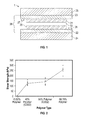
- FIG. 1 is a schematic cross-section of a multi-layer electrochromic device of the present disclosure.
- FIG. 2 is a plot illustrating variation in lap shear strength with polymer content.
- FIG. 3 is a stress-strain curve corresponding to a lap shear strength measurement, as more fully described in Example 3.
- FIG. 4 is an embodiment of a cross-section of a device during manufacturing.
- amine or “amino,” as used herein alone or as part of another group, represents a group of formula —N(R 8 )(R 9 ), wherein R 8 and R 9 are independently hydrogen, hydrocarbyl, substituted hydrocarbyl, silyl, or R 8 and R 9 taken together form a substituted or unsubstituted cyclic or polycyclic moiety, each as defined in connection with such terms, typically having from 3 to 8 atoms in the ring.
- Substituted amine refers to a group of formula —N(R 8 )(R 9 ), wherein at least one of R 8 and R 9 are other than hydrogen.
- Unsubstituted amine for example, refers to a group of formula —N(R 8 )(R 9 ), wherein R 8 and R 9 are both hydrogen.
- anodic electrochromic material refers to an electrochromic material that changes from a less optically transmissive state to a less optically transmissive state (e.g., darkens) upon oxidation (i.e., removal of electrons).
- aryl as used herein alone or as part of another group denotes optionally substituted homocyclic aromatic groups, preferably monocyclic or bicyclic groups containing from 6 to 12 carbons in the ring portion, such as phenyl, biphenyl, naphthyl, substituted phenyl, substituted biphenyl or substituted naphthyl. Phenyl and substituted phenyl are the more preferred aryl.
- each refers to the transition of an electrochromic material from a first optical state to a second optical state wherein the first optical state is less transmissive than the second optical state.
- bleached state voltage refers to the open circuit voltage (V oc ) of the anodic electrochromic layer versus Li/Li+ in an electrochemical cell in a propylene carbonate solution containing 1M lithium perchlorate when the transmissivity of said layer is at 95% of its “fully bleached state” transmissivity.
- cathodic electrochromic material refers to an electrochromic material that changes from a less optically transmissive state to a more optically transmissive state (e.g., darkens) upon reduction (i.e., addition of electrons).
- darken refers to the transition of an electrochromic material from a first optical state to a second optical state wherein the first optical state is more transmissive than the second optical state.
- electrochromic material refers to a material that is able to change its optical properties as a result of the insertion or extraction of ions and electrons.
- an electrochromic material may change between (i) a colored, translucent or opaque state and a transparent state or (ii) a colored, opaque state and a colored, translucent state.
- the change can be reversible while in other examples, the change can be irreversible.
- electrical potential refers to the voltage occurring across a device comprising an electrode/ion conductor/electrode stack.
- electrochemically matched refers to a set of cathode and anode electrochromic films or materials with similar charge capacities and complementary oxidation states such that when joined together by a suitable ion-conducting and electrically insulating layer, a functional electrochromic device is formed that shows reversible switching behavior over a substantial range of the theoretical charge capacities of the films or materials, respectively.
- electrode layer refers to a layer capable of conducting ions as well as electrons.
- the electrode layer contains a species that can be oxidized when ions are inserted into the material and contains a species that can be reduced when ions are extracted from the layer. This change in oxidation state of a species in the electrode layer is responsible for the change in optical properties in the device.
- the term “fully bleached state” as used in connection with an anodic electrochromic material refers to the state of maximum transmissivity of an anodic electrochromic layer in an electrochemical cell at or above 1.5V versus Li/Li+ in a propylene carbonate solution containing 1 M lithium perchlorate at 25° C. (under anhydrous conditions and in an Ar atmosphere).
- halide as used herein alone or as part of another group refer to chlorine, bromine, fluorine, and iodine.
- lap shear strength refers to the stress point at which either adhesive or cohesive failure occurs.
- sil as used herein describes substituents of the general formula —Si(X 8 )(X 9 )(X 10 ) where X 8 , X 9 , and X 10 are independently hydrocarbyl or substituted hydrocarbyl.
- substituted hydrocarbyl moieties described herein are hydrocarbyl moieties which are substituted with at least one atom other than carbon, including moieties in which a carbon chain atom is substituted with a hetero atom such as nitrogen, oxygen, silicon, phosphorous, boron, sulfur, or a halogen atom.
- substituents include halogen, heterocyclo, alkoxy, alkenoxy, alkynoxy, aryloxy, hydroxy, protected hydroxy, keto, acyl, acyloxy, nitro, amino, amido, nitro, cyano, thiol, ketals, acetals, esters, ethers, and thioethers.
- transmissive is used to denote transmission of electromagnetic radiation through a material.
- T vis is calculated/obtained by integrating the transmission spectrum in the wavelength range of 400-730 nm using the spectral photopic efficiency l_p(lambda) (CIE, 1924) as a weighting factor. (Ref: ASTM E1423).
- transparent is used to denote substantial transmission of electromagnetic radiation through a material such that, for example, bodies situated beyond or behind the material can be distinctly seen or imaged using appropriate image sensing technology.
- the present disclosure provides ion conducting polymers with sufficient cross-link densities to endure high levels of physical stress without limiting ion mobility, while remaining electrochemically stable.
- FIG. 1 depicts a cross-sectional structural diagram of electrochromic device 1 according to a first embodiment of the present disclosure.
- electrochromic device 1 comprises an ion conductor layer 10 .
- First electrode layer 20 is on one side of and in contact with a first surface of ion conductor layer 10
- second electrode layer 21 is on the other side of and in contact with a second surface of ion conductor layer 10 .
- at least one of first and second electrode layers 20 , 21 comprises electrochromic material; in one embodiment, first and second electrode layers 20 , 21 each comprise electrochromic material.
- the central structure that is, layers 20 , 10 , 21 , is positioned between first and second electrically conductive layers 22 and 23 which, in turn, are arranged against outer substrates 24 , 25 .
- Elements 22 , 20 , 10 , 21 , and 23 are collectively referred to as an electrochromic stack 28 .
- Electrically conductive layer 22 is in electrical contact with one terminal of a power supply (not shown) via bus bar 26 and electrically conductive layer 23 is in electrical contact with the other terminal of a power supply (not shown) via bus bar 27 whereby the transmissivity of electrochromic device 10 may be changed by applying a voltage pulse to electrically conductive layers 22 and 23 .
- the pulse causes electrons and ions to move between first and second electrode layers 20 and 21 and, as a result, electrochromic material in the first and/or second electrode layer(s) change(s) optical states, thereby switching electrochromic device 1 from a more transmissive state to a less transmissive state, or from a less transmissive state to a more transmissive state.
- electrochromic device 1 is transparent before the voltage pulse and less transmissive (e.g., more reflective or colored) after the voltage pulse or vice versa.
- the change in transmissivity may be a change from a first optical state to a second optical state that is (i) relatively more absorptive (i.e., less transmissive) than the first state, (ii) relatively less absorptive (i.e., more transmissive) than the first state, (iii) relatively more reflective (i.e., less transmissive) than the first state, (iv) relatively less reflective (i.e., more transmissive) than the first state, (v) relatively more reflective and more absorptive (i.e., less transmissive) than the first state or (vi) relatively less reflective and less absorptive (i.e., more transmissive) than the first state.
- the change may be between the two extreme optical states attainable by an electrochromic device, e.g., between a first transparent state and a second state, the second state being opaque or reflective (mirror).
- the change may be between two optical states, at least one of which is intermediate along the spectrum between the two extreme states (e.g., transparent and opaque or transparent and mirror) attainable for a specific electrochromic device.
- the corresponding device or process encompasses other optical state transitions such as non-reflective-reflective, transparent-opaque, etc.
- the term “bleached” refers to an optically neutral state, e.g., uncolored, transparent or translucent. Still further, unless specified otherwise herein, the “color” of an electrochromic transition is not limited to any particular wavelength or range of wavelengths. As understood by those of skill in the art, the choice of appropriate electrochromic and counter electrode materials governs the relevant optical transition.
- the change in transmissivity preferably comprises a change in transmissivity to electromagnetic radiation having a wavelength in the range of infrared to ultraviolet radiation.
- the change in transmissivity is predominately a change in transmissivity to electromagnetic radiation in the infrared spectrum.
- the change in transmissivity is to electromagnetic radiation having wavelengths predominately in the visible spectrum.
- the change in transmissivity is to electromagnetic radiation having wavelengths predominately in the ultraviolet spectrum.
- the change in transmissivity is to electromagnetic radiation having wavelengths predominately in the ultraviolet and visible spectra.
- the change in transmissivity is to electromagnetic radiation having wavelengths predominately in the infrared and visible spectra.
- the change in transmissivity is to electromagnetic radiation having wavelengths predominately in the ultraviolet, visible and infrared spectra.
- the materials making up electrochromic stack 28 may comprise organic or inorganic materials, and they may be solid or liquid.
- the electrochromic stack 28 comprises materials that are inorganic, solid (i.e., in the solid state), or both inorganic and solid.
- Inorganic materials have shown better reliability in architectural applications. Materials in the solid state can also offer the advantage of not having containment and leakage issues, as materials in the liquid state often do.
- any one or more of the layers in the stack may contain some amount of organic material, but in many implementations one or more of the layers contains little or no organic matter. The same can be said for liquids that may be present in one or more layers in small amounts.
- some or all of the materials making up electrochromic stack 28 are organic.
- Organic ion conductors can offer higher mobilities and thus potentially better device switching performance.
- Organic electrochromic layers can provide higher contrast ratios and more diverse color options. Each of the layers in the electrochromic device is discussed in detail, below. It should also be understood that solid state material may be deposited or otherwise formed by processes employing liquid components such as certain processes employing sol-gels or chemical vapor deposition.
- Ion conductor layer 10 serves as a medium through which ions are transported (in the manner of an electrolyte) when the electrochromic device switches between an optically less transmissive (“colored”) state and an optically more transmissive (“bleached”). Stated differently, the ion conducting layer permits sufficient ionic conduction between the first and second electrode layers 20 , 21 upon the application of a voltage across electrochromic stack 28 .
- ions include lithium ions (Li + ) and hydrogen ions (H + ) (i.e., protons). Other ions may also be employed in certain embodiments.
- ion conductor layer 10 has a lithium ion conductivity of at least about 10 ⁇ 5 S/cm at room temperature (i.e., 25° C.).
- ion conductor layer 10 has a lithium ion conductivity of at least about 10 ⁇ 4 S/cm at room temperature.
- ion conductor layer 10 has a lithium ion conductivity of at least about 10 ⁇ 3 S/cm at room temperature.
- ion conductor layer 10 has a lithium ion conductivity of at least about 10 ⁇ 2 S/cm at room temperature.
- ion conductor layer 10 has sufficiently low electron conductivity that negligible electron transfer takes place during normal operation.
- Ion conductor layer 10 is also preferably sufficiently durable so as to withstand repeated cycling of the electrochromic device between an optically less transmissive state and an optically more transmissive state.
- lithium ion conductivity of ion conductor layer 10 varies less than about 0.1% to about 5% upon cycling of the electrochromic device between a less transmissive state (e.g. about 5% transmissive) and a more transmissive state (e.g. about 70% transmissive) for at least 100 hours at 85° C.
- lithium ion conductivity of ion conductor layer 10 varies less than about 0.01% to about 2% upon cycling of the electrochromic device between a less transmissive state and a more transmissive state for at least 100 hours at 85° C.
- ion conductor layer 10 has a relatively low glass transition temperature (T g ), enabling the cured polymer network to remain soft and pliable upon exposure of electrochromic stack 28 to low environmental temperatures.
- T g glass transition temperature
- ion conductor layer 10 has a glass transition temperature of less than about ⁇ 5° C. to about ⁇ 40° C. and more particularly between the range of about ⁇ 10° C. to about ⁇ 25° C.
- the glass transition temperature of ion conductor layer 10 may be lowered under controlled conditions, e.g. the addition of a plasticizer, according to methods known in the art (see, e.g., U.S. Patent Publication No. 20120237704).
- the voltage applied across electrochromic stack 28 to reversibly switch electrochromic device between an optically less transmissive state and an optically more transmissive state is typically in the range of about 1 V to about ⁇ 4.5 V versus lithium (Li/Li + ).
- ion conducting layer be electrochemically stable (or within the electrochemical window) at voltages within this range.
- the ion conducting layer is electrochemically stable at voltages in the range of about 1.3 V and about 4.4 V relative to lithium (Li/Li + ).
- the ion conducting layer is electrochemically stable at voltages in the range of about 1.3 V and about 4 V relative to lithium (Li/Li + ).
- the ion conducting layer is electrochemically stable at voltages in the range of about 2 V and about 4 V relative to lithium (Li/Li + ).
- ion conductor layer 10 also possesses sufficient cohesion and adhesion to the first and second electrode layers 20 and 21 .
- ion conductor layer 10 has a lap shear strength of at least 100 kPa to at least 600 kPa, and more particularly between the range of 200 kPa to 400 kPa, as measured at 1.27 mm/min, at room temperature, in accordance with ASTM International standard D1002 or D3163.
- ion conductor layer 10 is elastically deformable.
- ion conductor layer 10 has an elongation to failure of at least 1 mm.
- electrolytes typically incorporated into ion conductor layer 10 are: solid polymer electrolytes (SPE), such as poly(ethylene oxide) with a dissolved lithium salt; gel polymer electrolytes (GPE), such as mixtures of poly(methyl methacrylate) and propylene carbonate with a lithium salt; composite gel polymer electrolytes (CGPE) that are similar to GPE's but with an addition of a second polymer such a poly(ethylene oxide), and liquid electrolytes (LE) such as a solvent mixture of ethylene carbonate/diethyl carbonate with a lithium salt; and composite organic-inorganic electrolytes (CE), comprising an LE with an addition of titania, silica or other oxides.
- SPE solid polymer electrolytes
- GPE gel polymer electrolytes
- CGPE composite gel polymer electrolytes
- LE liquid electrolytes
- CE composite organic-inorganic electrolytes
- lithium salts used are LiTFSl (lithium bis(trifluoromethane) sulfonimide), LiBF 4 (lithium tetrafluoroborate), LiAsF 6 (lithium hexafluoro arsenate), LiCF 3 SO 3 (lithium trifluoromethane sulfonate), and LiClO 4 (lithium perchlorate).
- suitable ion conducting layers include silicates, silicon oxides, tungsten oxides, tantalum oxides, niobium oxides, and borates.
- the silicon oxides include silicon-aluminum-oxide. These materials may be doped with different dopants, including lithium.
- Lithium doped silicon oxides include lithium silicon-aluminum-oxide.
- the ion conducting layer comprises a silicate-based structure.
- suitable ion conductors particularly adapted for lithium ion transport include, but are not limited to, lithium silicate, lithium aluminum silicate, lithium aluminum borate, lithium aluminum fluoride, lithium borate, lithium nitride, lithium zirconium silicate, lithium niobate, lithium borosilicate, lithium phosphosilicate, and other such lithium-based ceramic materials, silicas, or silicon oxides, including lithium silicon-oxide.
- the thickness of the ion conductor layer 10 will vary depending on the material. In some embodiments using an inorganic ion conductor the ion conductor layer 10 is about 250 nm to 1 nm thick, and more particularly about 50 nm to 5 nm thick. In some embodiments using an organic ion conductor, the ion conducting layer is between about 1 ⁇ m and 1000 ⁇ m thick or, more particularly, between about 100 ⁇ m and 500 ⁇ m thick. The thickness of the ion conducting layer is also substantially uniform. In one embodiment, a substantially uniform ion conducting layer varies by not more than about +/ ⁇ 10% in each of the aforementioned thickness ranges.
- a substantially uniform ion conducting layer varies by not more than about +/ ⁇ 5% in each of the aforementioned thickness ranges. In another embodiment, a substantially uniform ion conducting layer varies by not more than about +/ ⁇ 3% in each of the aforementioned thickness ranges.
- the power supply (not shown) connected to bus bars 26 , 27 is typically a voltage source with optional current limits or current control features and may be configured to operate in conjunction with local thermal, photosensitive or other environmental sensors.
- the voltage source may also be configured to interface with an energy management system, such as a computer system that controls the electrochromic device according to factors such as the time of year, time of day, and measured environmental conditions.
- an energy management system in conjunction with large area electrochromic devices (e.g., an electrochromic architectural window), can dramatically lower the energy consumption of a building.
- At least one of the substrates 24 , 25 is preferably transparent, in order to reveal the electrochromic properties of the stack 28 to the surroundings.
- Any material having suitable optical, electrical, thermal, and mechanical properties may be used as first substrate 24 or second substrate 25 .
- Such substrates include, for example, glass, plastic, metal, and metal coated glass or plastic.
- Non-exclusive examples of possible plastic substrates are polycarbonates, polyacrylics, polyurethanes, urethane carbonate copolymers, polysulfones, polyimides, polyacrylates, polyethers, polyester, polyethylenes, polyalkenes, polyimides, polysulfides, polyvinylacetates and cellulose-based polymers.
- a plastic substrate may be barrier protected and abrasion protected using a hard coat of, for example, a diamond-like protection coating, a silica/silicone anti-abrasion coating, or the like, such as is well known in the plastic glazing art.
- Suitable glasses include either clear or tinted soda lime glass, including soda lime float glass. The glass may be tempered or untempered.
- electrochromic device 1 with glass e.g.
- soda lime glass used as first substrate 24 and/or second substrate 25 , there is a sodium diffusion barrier layer (not shown) between first substrate 24 and first electrically conductive layer 22 and/or between second substrate 25 and second electrically conductive layer 23 to prevent the diffusion of sodium ions from the glass into first and/or second electrically conductive layer 23 .
- second substrate 25 is omitted.
- the substrate first and or second substrates may also be a composite of two or materials.
- Thin glass or plastic substrates may be used to manufacture the electrochromic device and may be laminated to a thicker carrier glass to provide mechanical strength and durability to large scale products incorporating the electrochromic devices.
- the carrier glass is tempered glass.
- the thicker carrier glass may be laminated to the thinner substrates prior to deposition of the layers of the electrochromic device or after the completion of the device and the lamination of the ion conductor. Additionally there may be more than one electrochromic device formed on thin glass or plastic laminated to carrier glass, thereby increasing the possible strain on the device.
- the use of carrier glass increases the weight and embodiments of the current invention may be advantageous in maintaining the durability and mechanical strength of devices according to embodiments of this disclosure.
- the tunability of the ion conductor to provide the desired bonding strength once cross-linked is an advantage in these embodiments.
- an Insulated Glass Unit there are typically at least two complete electrochromic devices integrated on each of the panes. In some embodiments there may be more than two panes having electrochromic devices or an additional pane of glass only to increase the insulative properties of the IGU.
- first substrate 24 and second substrate 25 are each float glass.
- this glass is at least 0.5 meters by 0.5 meters, and can be much larger, e.g., as large as about 3 meters by 4 meters. In such applications, this glass is typically at least about 2 mm thick and more commonly 4-6 mm thick.
- the electrochromic devices of the present disclosure may have a wide range of sizes.
- the electrochromic device comprise a substrate having a surface with a surface area of at least 0.001 meter 2 .
- the electrochromic device comprises a substrate having a surface with a surface area of at least 0.01 meter 2 .
- the electrochromic device comprises a substrate having a surface with a surface area of at least 0.1 meter 2 .
- the electrochromic device comprises a substrate having a surface with a surface area of at least 1 meter 2 .
- the electrochromic device comprises a substrate having a surface with a surface area of at least 5 meter 2 .
- the electrochromic device comprises a substrate having a surface with a surface area of at least 10 meter 2 .
- At least one of the two electrically conductive layers 22 , 23 is also preferably transparent in order to reveal the electrochromic properties of the stack 28 to the surroundings.
- electrically conductive layer 23 is transparent.
- electrically conductive layer 22 is transparent.
- electrically conductive layers 22 , 23 are each transparent.
- one or both of the electrically conductive layers 22 , 23 is inorganic and/or solid. Electrically conductive layers 22 and 23 may be made from a number of different transparent materials, including transparent conductive oxides, thin metallic coatings, networks of conductive nano particles (e.g., rods, tubes, dots) conductive metal nitrides, and composite conductors.
- Transparent conductive oxides include metal oxides and metal oxides doped with one or more metals.
- metal oxides and doped metal oxides include indium oxide, indium tin oxide, doped indium oxide, tin oxide, doped tin oxide, zinc oxide, aluminum zinc oxide, doped zinc oxide, ruthenium oxide, doped ruthenium oxide and the like.
- Transparent conductive oxides are sometimes referred to as (TCO) layers.
- Thin metallic coatings that are substantially transparent may also be used. Examples of metals used for such thin metallic coatings include gold, platinum, silver, aluminum, nickel, and alloys of these.
- transparent conductive nitrides examples include titanium nitrides, tantalum nitrides, titanium oxynitrides, and tantalum oxynitrides.
- Electrically conducting layers 22 and 23 may also be transparent composite conductors. Such composite conductors may be fabricated by placing highly conductive ceramic and metal wires or conductive layer patterns on one of the faces of the substrate and then over-coating with transparent conductive materials such as doped tin oxides or indium tin oxide. Ideally, such wires should be thin enough as to be invisible to the naked eye (e.g., about 100 ⁇ m or thinner).
- Non-exclusive examples of electron conductors 22 and 23 transparent to visible light are thin films of indium tin oxide (ITO), tin oxide, zinc oxide, titanium oxide, n- or p-doped zinc oxide and zinc oxyfluoride.
- ITO indium tin oxide
- Metal-based layers, such as ZnS/Ag/ZnS and carbon nanotube layers have been recently explored as well.
- one or both electrically conductive layers 22 and 23 may be made of or include a metal grid.
- the thickness of the electrically conductive layer may be influenced by the composition of the material comprised within the layer and its transparent character.
- electrically conductive layers 22 and 23 are transparent and each have a thickness that is between about 1000 nm and about 50 nm. In some embodiments, the thickness of electrically conductive layers 22 and 23 is between about 500 nm and about 100 nm. In other embodiments, the electrically conductive layers 22 and 23 each have a thickness that is between about 400 nm and about 200 nm. In general, thicker or thinner layers may be employed so long as they provide the necessary electrical properties (e.g., conductivity) and optical properties (e.g., transmittance). For certain applications it will generally be preferred that electrically conductive layers 22 and 23 be as thin as possible to increase transparency and to reduce cost.
- the function of the electrically conductive layers is to apply the electric potential provided by a power supply over the entire surface of the electrochromic stack 28 to interior regions of the stack.
- the electric potential is transferred to the conductive layers though electrical connections to the conductive layers.
- bus bars one in contact with first electrically conductive layer 22 and one in contact with second electrically conductive layer 23 provide the electric connection between the voltage source and the electrically conductive layers 22 and 23 .
- the sheet resistance, R s , of the first and second electrically conductive layers 22 and 23 is about 500 ⁇ / ⁇ to 1 ⁇ / ⁇ . In some embodiments, the sheet resistance of first and second electrically conductive layers 22 and 23 is about 100 ⁇ / ⁇ to 5 ⁇ / ⁇ . In general, it is desirable that the sheet resistance of each of the first and second electrically conductive layers 22 and 23 be about the same. In one embodiment, first and second electrically conductive layers 22 and 23 each have a sheet resistance of about 20 ⁇ / ⁇ to about 8 ⁇ / ⁇ .
- At least one of electrically conductive layers 22 , 23 preferably has a sheet resistance, R s , to the flow of electrons through the layer that is non-uniform.
- R s sheet resistance
- first and second electrically conductive layers 22 , 23 has a non-uniform sheet resistance to the flow of electrons through the layer.
- first electrically conductive layer 22 and second electrically conductive layer 23 each have a non-uniform sheet resistance to the flow of electrons through the respective layers.
- spatially varying the sheet resistance of electrically conductive layer 22 improves the switching performance of the device by controlling the voltage drop in the conductive layer to provide uniform potential drop or a desired non-uniform potential drop across the device, over the area of the device.
- electrical circuit modeling may be used to determine the sheet resistance distribution providing desired switching performance, taking into account the type of electrochromic device, the device shape and dimensions, electrode characteristics, and the placement of electrical connections (e.g., bus bars) to the voltage source.
- the sheet resistance distribution in turn, can be controlled, at least in part, by grading the thickness of the first and/or second electrically conductive layer(s), grading the composition of the first and/or second electrically conductive layer(s), or patterning the first and/or second electrically conductive layer(s), or some combination of these.
- the electrochromic device is a rectangular electrochromic window.
- first substrate 24 and second substrate 25 are rectangular panes of glass or other transparent substrate and electrochromic device 1 has two bus bars 26 , 27 located on opposite sides of first electrode layer 20 and second electrode layer 21 , respectively.
- electrochromic device 1 has two bus bars 26 , 27 located on opposite sides of first electrode layer 20 and second electrode layer 21 , respectively.
- the resistance to the flow of electrons in first electrically conductive layer 22 increases with increasing distance from bus bar 26 and that the resistance to the flow of electrons in second electrically conductive layer 23 increases with increasing distance from bus bar 27 .
- This can be effected, for example, by decreasing the thickness of first electrically conductive layer 22 as a function of increasing distance from bus bar 26 and decreasing the thickness of second electrically conductive layer 23 as a function of increasing distance from bus bar 27 .
- the multi-layer devices of the present disclosure may have a shape other than rectangular, may have more than two bus bars, and/or may not have the bus bars on opposite sides of the device.
- the multi-layer device may have a perimeter that is more generally a quadrilateral, or a shape with greater or fewer sides than four for example, the multi-layer device may be triangular, pentagonal, hexagonal, etc., in shape.
- the multi-layer device may have a perimeter that is curved but lacks vertices, e.g., circular, oval, etc.
- the multi-layer device may comprise three, four or more bus bars connecting the multi-layer device to a voltage source, or the bus bars, independent of number may be located on non-opposing sides.
- the preferred resistance profile in the electrically conductive layer(s) may vary from that which is described for the rectangular, two bus bar configuration.
- first and second electrode layers 20 and 21 are electrochromic, one of the first and second electrode layers is the counter electrode for the other, and first and second electrode layers 20 and 21 are inorganic and/or solid.
- electrochromic electrode layers 20 and 21 are cathodically coloring thin films of oxides based on tungsten, molybdenum, niobium, titanium, lead and/or bismuth, or anodically coloring thin films of oxides, hydroxides and/or oxy-hydrides based on nickel, iridium, iron, chromium, cobalt and/or rhodium.
- first electrode layer 20 contains any one or more of a number of different electrochromic materials, including metal oxides.
- metal oxides include tungsten oxide (WO 3 ), molybdenum oxide (MoO 3 ), niobium oxide (Nb 2 O 5 ), titanium oxide (TiO 2 ), copper oxide (CuO), iridium oxide (Ir 2 O 3 ), chromium oxide (Cr 2 O 3 ), manganese oxide (Mn 2 O 3 ), vanadium oxide (V 2 O 3 ), nickel oxide (Ni 2 O 3 ), cobalt oxide (Co 2 O 3 ) and the like.
- the metal oxide is doped with one or more dopants such as lithium, sodium, potassium, molybdenum, vanadium, titanium, and/or other suitable metals or compounds containing metals.
- dopants such as lithium, sodium, potassium, molybdenum, vanadium, titanium, and/or other suitable metals or compounds containing metals.
- Mixed oxides e.g., W—Mo oxide, W—V oxide are also used in certain embodiments.
- first electrode layer 20 is electrochromic and is made substantially of WO x , where “x” refers to an atomic ratio of oxygen to tungsten in the electrochromic layer, and x is between about 2.7 and 3.5.
- the electrochromic mixed metal oxide is crystalline, nanocrystalline, or amorphous.
- the tungsten oxide is substantially nanocrystalline, with grain sizes, on average, from about 5 nm to 50 nm (or from about 5 nm to 20 nm), as characterized by transmission electron microscopy (TEM).
- TEM transmission electron microscopy
- the tungsten oxide morphology may also be characterized as nanocrystalline using x-ray diffraction (XRD); XRD.
- nanocrystalline electrochromic tungsten oxide may be characterized by the following XRD features: a crystal size of about 10 to 100 nm (e.g., about 55 nm.
- nanocrystalline tungsten oxide may exhibit limited long range order, e.g., on the order of several (about 5 to 20) tungsten oxide unit cells.
- first electrode layer 20 depends on the electrochromic material selected for the electrochromic layer. In some embodiments, first electrode layer 20 is about 50 nm to 2,000 nm, or about 100 nm to 700 nm. In some embodiments, the first electrode layer 20 is about 250 nm to about 500 nm.
- Second electrode layer 21 serves as the counter electrode to first electrode layer 20 and, like first electrode layer 20 , second electrode layer 21 may comprise electrochromic materials as well as non-electrochromic materials.
- Non-exclusive examples of second electrode layer 21 are cathodically coloring electrochromic thin films of oxides based on tungsten, molybdenum, niobium, titanium, lead and/or bismuth, anodically coloring electrochromic thin films of oxides, hydroxides and/or oxy-hydrides based on nickel, iridium, iron, chromium, cobalt and/or rhodium, or non-electrochromic thin films, e.g., of oxides based on vanadium and/or cerium as well as activated carbon. Also combinations of such materials can be used as second electrode layer 21 .
- second electrode layer 21 may comprise one or more of a number of different materials that are capable of serving as reservoirs of ions when the electrochromic device is in the bleached state.
- the counter electrode layer transfers some or all of the ions it holds to the electrochromic first electrode layer 20 , changing the electrochromic first electrode layer 20 to the colored state.
- suitable materials for a counter electrode complementary to WO 3 include nickel oxide (NiO), nickel tungsten oxide (NiWO), nickel vanadium oxide, nickel chromium oxide, nickel aluminum oxide, nickel manganese oxide, nickel magnesium oxide, chromium oxide (Cr 2 O 3 ), manganese oxide (MnO 2 ), and Prussian blue.
- Optically passive counter electrodes comprise cerium titanium oxide (CeO 2 —TiO 2 ), cerium zirconium oxide (CeO 2 —ZrO 2 ), nickel oxide (NiO), nickel-tungsten oxide (NiWO), vanadium oxide (V 2 O 5 ), and mixtures of oxides (e.g., a mixture of Ni 2 O 3 and WO 3 ).
- first electrode layer 20 contains the ions used to produce the electrochromic phenomenon in the electrochromic material when the electrochromic material is in the bleached state
- the counter electrode preferably has high transmittance and a neutral color when it holds significant quantities of these ions.
- nickel-tungsten oxide is used in the counter electrode layer.
- the amount of nickel present in the nickel-tungsten oxide can be up to about 90% by weight of the nickel-tungsten oxide.
- the mass ratio of nickel to tungsten in the nickel-tungsten oxide is between about 4:6 and 6:4 (e.g., about 1:1).
- the NiWO is between about 15% (atomic) Ni and about 60% Ni; between about 10% W and about 40% W; and between about 30% O and about 75% O.
- the thickness of second electrode layer 21 is about 50 nm about 650 nm. In some embodiments, the thickness of second electrode layer 21 is about 100 nm to about 400 nm, preferably in the range of about 200 nm to 300 nm.
- substrates 24 and 25 have flat surfaces. That is, they have a surface coincides with the tangential plane in each point.
- substrates with flat surfaces are typically employed for electrochromic architectural windows and many other electrochromic devices, it is contemplated that the multi-layer devices of the present disclosure may have a single or even a doubly curved surface.
- each of the layers of stack 28 have a corresponding radius of curvature. See, for example, U.S. Pat. No. 7,808,692 which is incorporated herein by reference in its entirety with respect to the definition of single and doubly curved surfaces and methods for the preparation thereof.
- ion conductor layer 10 is produced from a liquid ion conducting polymer feedstock that comprises a monomer, oligomer, or mixture of monomers and/or oligimers, a plasticizer, and an ionizable charge carrier such as a lithium salt.
- the ion conducting polymer feedstock may additionally comprise a cross-linking catalyst and/or a viscosity increasing agent.
- the ion conducting polymer feedstock imparts certain mechanical and electrochemical properties to ion conductor layer 10 .
- the respective components of the ion conducting polymer feedstock i.e.
- the ion conducting polymer feedstock may also comprise other additives to promote device performance such as moisture reduction additives (e.g. nanoparticles of molecular sieves or fumed silica), UV stabilizers, pH buffers, and the like.
- moisture reduction additives e.g. nanoparticles of molecular sieves or fumed silica
- UV stabilizers e.g. UV stabilizers, pH buffers, and the like.
- Typical monomers, oligomers, or mixtures of monomers and/or oligomers used in the ion conducting polymer feedstock may comprise, for example, at least one functional group selected from the group of epoxy, hydroxyl, carbonyl, sulfonyl, ethylene, styrene, vinyl, isocyanate, and acrylate, or repeat units of siloxane, polysulfone, or an oligomer comprising one or more of the listed functional groups.
- the selected monomer or oligomer may be cyclic or, more preferably, aliphatic.
- the selected monomer(s) or oligomer(s) may comprise monofunctional or polyfunctional (e.g. difunctional or trifunctional) monomer repeat unit(s), i.e.
- the density of the crosslink within ion conducting layer 10 tends to increase with the amount and/or the degree of polyfunctional monomer present in the ion conducting polymer feedstock.
- an ion conducting polymer feedstock having a ratio of polyfunctional monomer (e.g. diepoxide) to monofunctional monomer e.g.
- ion conducting layer having lower ion mobility and higher lap shear strength than an ion conductor layer produced from a feedstock having a polyfunctional monomer to monofunctional monomer ratio of 1:1.
- Other variations in ion conducting polymer feedstock such as polymer backbone rigidity may also affect the mechanical and electrochemical properties of ion conducting layer 10 .
- a pre-formed polymer having crosslinkable functionality such as glycidyl methacrylate (GMA) or poly-GMA, may be used in place of the monomer(s), oligomer(s), or mixture of monomer(s) and/or oligomer(s) in the ion conducting formulation.
- the pre-formed polymer may be polyethylene glycol methyl ether methacrylate (PEGMEMA) in combination with poly-GMA.
- PEGMEMA polyethylene glycol methyl ether methacrylate
- the ratio of poly-EGMEMA to poly-GMA units in the pre-formed polymer may be in the range of approximately 1:1 to 9:1.
- the monomer(s), oligomer(s), or mixture of monomer(s) and/or oligomer(s) is/are present in the ion conducting polymer feedstock in an amount ranging from about 0 wt. % to 90 wt. % of the of the total ion conducting polymer feedstock formulation.
- the monomer(s), oligomer(s), or mixture of monomer(s) and/or oligomer(s) is/are present in an amount ranging from 5 wt. % to 50 wt. % of the of the total mass of ion conducting polymer feedstock.
- the monomer(s), oligomer(s), or mixture of monomer(s) and/or oligomer(s) is/are present at about 30 wt. % of the total mass of ion conducting polymer feedstock.
- the monomer(s), oligomer(s), or mixture of monomer(s) and/or oligomer(s) may preferably contain polyfunctional monomer in an amount ranging between about 0 wt. % and about 25 wt. % of the total mass of ion conducting polymer feedstock, varied relative to monofunctional monomer to optimize mechanical and electrochemical device properties.
- polyfunctional monomer feedstock having difunctional and monofunctional monomer in a ratio of about 3:1 will produce an ion conducting layer having a higher cross-link density than a feedstock having a 1:1 difunctional to monofunctional monomer ratio.
- This higher cross-link density would be expected to reduce ion mobility and may affect switching kinetics between less transmissive and more transmissive states. Additionally, higher cross-link density may also affect the adhesive and cohesive properties (as measured by lap shear tests) of the ion conducting layer.
- the plasticizer of the ion conducting polymer feedstock may be any known plasticizer for electrochromic or battery systems, such as sulfolane, 3-methyl sulfolane, propylene carbonate, ethylene carbonate, or polyethylene glycol dimethyl ether, optionally combined with a viscosity-increasing agent.
- the plasticizer is sulfolane, as ion conducting layers comprising sulfolane possess enhanced durability and color characteristics for the applications described elsewhere in this application over those ion conducting layers comprising propylene carbonate or polyethylene glycol dimethyl ether.
- plasticizer is present in the ion conducting polymer feedstock in an amount ranging from 10 wt. % to 90 wt. % of the of the total ion conducting polymer feedstock formulation.
- plasticizer is present in the ion conducting polymer feedstock in an amount ranging from 40 wt. % to 60 wt. % of the total ion conducting polymer feedstock formulation.
- the monomer(s), oligomer(s), or mixture of monomer(s) and/or oligomer(s) may be polymerized and cross-linked in situ where the polymerization reaction is initiated by a cross-linking catalyst comprising an ionizable charge carrier, preferably by cationic initiation.
- the source of the ionic charge carrier may be selected from a lithium ion source, a sodium ion source, a potassium ion source, or a proton source.
- the source of the ionizable charge carrier is lithium bis-trifluoromethanesulfonimide (LiTFSi).
- one or more Lewis or BrOnsted acids such as BF 3 , trifilic acid, mesic acid, trifluoroacetic acid, and nanozeolites, may be added to the liquid formulation where necessary or desired to catalyze the polymerization reaction.
- free standing fully formulated ion conducting films may be used in place of the crosslinking ion conducting formulation or the liquid ion conducting formulation may be used in a “cast in place” process where a pre-formed cavity between the anode and cathode is produced (edge sealed) and the formulation is forced into this cavity through fill ports.
- the ion conducting polymer feedstock comprises a viscosity-increasing agent.
- the viscosity-increasing agent may be any polymer compatible with the polymerization system, whether or not the polymer contains a reactive functional group. Suitable polymers include, for example, cellulose and cellulose derivatives (e.g. cellulose acetate, cellulose triacetate, cellulose propionate acetate, ethyl cellulose, methylcellulose, etc.), polysulfones, and polymer esters.
- the durability of the ion conducting layer may be improved where the viscosity-increasing agent lacks amine functionality and is substantially free of polyethylene glycol.
- the coloring of the ion conducting layer may shift from more yellow to less yellow or colorless where the viscosity-increasing agent is aliphatic and/or lacking amine functionality.
- the viscosity increasing agent may be anhydrous to prevent electrolysis under the conditions of cycling.
- the viscosity increasing agent may be solid and inert.
- the viscosity-increasing agent may comprise an aggregation of particles such as fumed silica.
- the ion conductor polymer feedstock may be stored for a period of time prior to use in forming an ion conducting layer.
- the ion conducting polymer feedstock may be formulated in two or more distinct components and stored in separate containers.
- the first component may comprise a monomer, oligomer, or mixture of monomers and/or oligomers
- the second component may comprise a cross-linking catalyst (i.e. an ionizable charge carrier and/or acid)
- either the first component or the second component or both may comprise other additives such as a plasticizer or viscosity-increasing agent.
- the separately-stored monomer and cross-linking catalyst components may be mixed at the point of deposition onto a substrate in proportions sufficient to result in the desired cross-linking density upon polymerization.
- the ion conducting polymer feedstock may be formulated in a single container comprising monomer(s), oligomer(s), or mixture of monomer(s) and/or oligomer(s), a cross-linking catalyst, and other additives such as a plasticizer or viscosity-increasing agent.
- a single-container ion conducting feedstock may be used where the monomer and cross-linking catalyst components remain unreacted until an external energy source such as thermal or UV radiation is applied to the system to initiate polymerization and cross-linking.
- the viscosity of the ion conducting formulation as dispensed may be engineered to achieve a desired viscosity.
- the ion conducting formulation as dispensed may, for example, have a viscosity of between about 15,000 cP and about 100,000 cP at room temperature (i.e. 25° C.).
- the ion conducting formulation as dispensed may have a viscosity of between about 20,000 cP and 50,000 cP at room temperature.
- the ion conducting formulation as dispensed may have a viscosity of between about 25,000 cP and 35,000 cP at room temperature.
- the ion conducting formulation as dispensed may have a viscosity of about 30,000 cP at room temperature.
- each of the monomer component and the cross-linking catalyst component may be engineered to achieve a desired viscosity upon mixing of the two components for dispense (e.g. dispense from a nozzle onto a substrate).
- viscosity of the monomer component is typically increased by the addition of a viscosity-increasing agent to be substantially higher than the desired dispense viscosity.
- the viscosity of the cross-linking catalyst component is substantially lower than the desired dispense viscosity.
- a monomer component comprising an epoxy monomer may have a viscosity of about 40,000 cP at room temperature (i.e. 25° C.) and a cross-linking catalyst component may have a viscosity of about 5,000 cP at room temperature, where viscosity of the mixed monomer component and catalyst component as dispensed is between about 25,000 cP and about 35,000 cP, or more preferably about 30,000 cP, at room temperature.
- the ion conducting layer incorporated into the multi-layer structures of the present disclosure may be prepared by a number of deposition processes including wet-coating, spray coating, dip coating, roller coating, blade coating, screen printing, and nozzle application by a single jet, multiple jets, or an array of nozzles.
- ion conductor layer 10 may be incorporated into electrochromic multi-layer stack 28 by a series of steps involving dispensing the ion conducing formulation then laminating and curing the stack.
- ion conducting polymer feedstock is deposited or dispensed from a nozzle onto a first multi-layer stack comprising a first substrate and a first electrode layer.
- a second multi-layer stack comprising a second electrode layer and a second substrate is subsequently laminated onto the first multi-layer stack to form an electrochromic multi-layer stack comprising, in succession, the first substrate, the first electrode layer, the ion conducting formulation layer, the second electrode layer, and the second substrate, the first electrode layer, the second electrode layer, or both comprising an electrochromic material.
- the first or second or both the first and second multi-layer stack(s) may comprise a polyisobutylene (FIB) seal around the edge forming a barrier between the environment and the ion conducting formulation layer.
- the lamination step comprises vacuum sealing of the first and second multi-layer stacks at 1 torr to remove air and press the ion conducting formulation layer to uniform thickness.
- the vacuum-sealed multi-layer stack may be heated to between about 80° C. and about 150° C. to further seal the multi-layer stack, initiate polymerization and cross-linking, and melt polyisobutylene.
- Curing may occur by continuing to apply heat or other electromagnetic radiation such as ultraviolet, infrared, or gamma radiation.
- curing may occur by application of ultraviolet radiation for about 5 seconds.
- curing may occur by application of heat for not less than 5 minutes.
- curing may occur upon application of heat or electromagnetic radiation for between 10 minutes and 2 hours, between 15 minutes and 1 hour, or between 15 and 20 minutes.
- curing may occur upon application of heat or electromagnetic radiation over a period of hours or days.
- curing may occur upon application of heat or electromagnetic radiation over a period of hours or days.
- curing may occur upon application of heat or electromagnetic radiation for at least 16 hours.
- anodically coloring electrochromic materials and/or cathodically coloring electrochromic materials are prepared using thin-film deposition techniques.
- the resulting anodic and cathodic electrochromic films have a range of desirable properties and characteristics.
- the anodic electrochromic material may have a bleached state voltage value significantly greater than 2.0V.
- the anodic electrochromic material is provided in an electrochemically matched state relative to a cathodic electrochromic material in its fully bleached state for use in an electrochromic device.
- the anodic electrochromic material is relatively stable; for example, the lithium nickel oxide material does not darken from its fully bleached state or deactivate (e.g., remain transparent but no longer function as an electrochromic anode material or film) at elevated temperatures in the presence of ambient air.
- the electrochromic materials comprised by the anode electrode (i.e., the first or second electrode 20 , 21 ; see FIG. 1 ) of a multi-layer structure of the present disclosure are inorganic or organometallic and the electrochromic materials comprised by the cathode (i.e., the other of the first or second electrode 20 , 21 ; see FIG. 1 ) are independently inorganic or organometallic.
- the electrochromic materials comprised by the anode and/or the cathode are inorganic or organometallic solid state materials with 3-D framework structures comprising metals bridged or separated by anionic atoms or molecules such as oxide, hydroxide, phosphate, cyanide, halide, that further comprise mobile ions such as protons, lithium, sodium, potassium that can intercalate and de-intercalate as the material is reduced or oxidized during the electrochromic cycle.
- the anodic and cathodic films incorporated into the multi-layer structures of the present disclosure may be prepared by a number of deposition processes including vapor deposition processes, wet-coating processes, spray coating processes, dip coating, and electrodeposition.
- a first mixture is prepared by combining 60 g of sulfolane, 40 g of LiTFSi and 1 g of a BF 3 solution (10 mg BF 3 .OEt 2 in sulfolane).
- a second mixture is prepared by combining 60 g of sulfolane, 15 g of cellulose acetate (40K MW), 22.5 g of butyl glycidyl ether and 2.5 g of diglycidyl cyclohexanedicarboxylate.
- the first mixture and second mixture are combined immediately prior to dispense from a nozzle to form an ion conducting polymer feedstock having a viscosity of approximately 25,000 cP at room temperature.
- a first mixture is prepared by combining 60 g of sulfolane, 40 g of LiTFSi and 1 g of a BF 3 solution (10 mg BF 3 .OEt 2 in sulfolane).
- a second mixture is prepared by combining 60 g of sulfolane, 15 g of cellulose acetate (40K MW), 17.5 g of butyl glycidyl ether and 7.5 g of diglycidyl cyclohexanedicarboxylate.
- the first mixture and second mixture are combined immediately prior to dispense from a nozzle to form an ion conducting polymer feedstock having a viscosity of approximately 25,000 cP at room temperature.
- an edge seal B comprising polyisobutylene is deposited on the perimeter of a first electrode A.
- the ion conducting polymer feedstock C of Example 2 is coated onto first electrode B using a slot die, a spray coater, a wire bar coater, or a roller coater without contacting the edge seal B.
- a second electrode D is then paired with first electrode A supporting the ion conducting polymer feedstock and laminated to form multi-layer stack E.
- the ion conducting polymer feedstock spreads evenly to cover the space between first electrode A and second electrode C.
- Edge seal B is compressed and becomes directly adjacent to the ion conductor layer.
- the laminate is cured at 150° C. for 16 hours. Lap shear strength of the ion conductor layer after cure is about 180 kPa, as measured at 1.27 mm at room temperature according to ASTM D3163.
Abstract
Description
Claims (12)
Priority Applications (4)
| Application Number | Priority Date | Filing Date | Title |
|---|---|---|---|
| US14/994,090 US9720299B1 (en) | 2015-01-12 | 2016-01-12 | Electrochromic multi-layer devices with cross-linked ion conducting polymer |
| US15/662,740 US10723835B2 (en) | 2015-01-12 | 2017-07-28 | Electrochromic multi-layer devices with cross-linked ion conducting polymer |
| US16/940,169 US11708449B2 (en) | 2015-01-12 | 2020-07-27 | Electrochromic multi-layer devices with cross-linked ion conducting polymer |
| US18/333,790 US20230323014A1 (en) | 2015-01-12 | 2023-06-13 | Electrochromic multi-layer devices with cross-linked ion conducting polymer |
Applications Claiming Priority (2)
| Application Number | Priority Date | Filing Date | Title |
|---|---|---|---|
| US201562102401P | 2015-01-12 | 2015-01-12 | |
| US14/994,090 US9720299B1 (en) | 2015-01-12 | 2016-01-12 | Electrochromic multi-layer devices with cross-linked ion conducting polymer |
Related Child Applications (1)
| Application Number | Title | Priority Date | Filing Date |
|---|---|---|---|
| US15/662,740 Division US10723835B2 (en) | 2015-01-12 | 2017-07-28 | Electrochromic multi-layer devices with cross-linked ion conducting polymer |
Publications (1)
| Publication Number | Publication Date |
|---|---|
| US9720299B1 true US9720299B1 (en) | 2017-08-01 |
Family
ID=59383359
Family Applications (4)
| Application Number | Title | Priority Date | Filing Date |
|---|---|---|---|
| US14/994,090 Active - Reinstated US9720299B1 (en) | 2015-01-12 | 2016-01-12 | Electrochromic multi-layer devices with cross-linked ion conducting polymer |
| US15/662,740 Active 2036-01-18 US10723835B2 (en) | 2015-01-12 | 2017-07-28 | Electrochromic multi-layer devices with cross-linked ion conducting polymer |
| US16/940,169 Active 2037-03-25 US11708449B2 (en) | 2015-01-12 | 2020-07-27 | Electrochromic multi-layer devices with cross-linked ion conducting polymer |
| US18/333,790 Pending US20230323014A1 (en) | 2015-01-12 | 2023-06-13 | Electrochromic multi-layer devices with cross-linked ion conducting polymer |
Family Applications After (3)
| Application Number | Title | Priority Date | Filing Date |
|---|---|---|---|
| US15/662,740 Active 2036-01-18 US10723835B2 (en) | 2015-01-12 | 2017-07-28 | Electrochromic multi-layer devices with cross-linked ion conducting polymer |
| US16/940,169 Active 2037-03-25 US11708449B2 (en) | 2015-01-12 | 2020-07-27 | Electrochromic multi-layer devices with cross-linked ion conducting polymer |
| US18/333,790 Pending US20230323014A1 (en) | 2015-01-12 | 2023-06-13 | Electrochromic multi-layer devices with cross-linked ion conducting polymer |
Country Status (1)
| Country | Link |
|---|---|
| US (4) | US9720299B1 (en) |
Cited By (13)
| Publication number | Priority date | Publication date | Assignee | Title |
|---|---|---|---|---|
| WO2018204719A1 (en) | 2017-05-03 | 2018-11-08 | Kinestral Technologies, Inc. | Flexible and multilayer electrochromic devices and methods of making the same |
| US20190379085A1 (en) * | 2018-06-08 | 2019-12-12 | Solid State Battery Incorporated | Composite solid polymer electrolytes for energy storage devices |
| US10667417B2 (en) * | 2016-11-10 | 2020-05-26 | Samsung Display Co., Ltd. | Cover window for display device and display device including the same |
| US10775649B2 (en) | 2018-05-17 | 2020-09-15 | Cardinal Cg Company | Elastomeric optical device and related methods |
| CN112987427A (en) * | 2019-12-14 | 2021-06-18 | 传奇视界有限公司 | Electro-dimming glass and preparation method thereof |
| US20210273291A1 (en) * | 2017-11-28 | 2021-09-02 | Quantumscape Battery, Inc. | Catholyte management for a solid-state separator |
| US11221534B2 (en) | 2018-03-05 | 2022-01-11 | Heliotrope Technologies, Inc. | Methods of manufacturing electrochromic devices containing a solid-state electrolyte |
| US11289700B2 (en) | 2016-06-28 | 2022-03-29 | The Research Foundation For The State University Of New York | KVOPO4 cathode for sodium ion batteries |
| US11340479B2 (en) | 2018-05-17 | 2022-05-24 | Cardinal Cg Company | Elastomeric optical device and related operation methods |
| US11409176B2 (en) | 2017-12-26 | 2022-08-09 | Heliotrope Europe S.L. | Gel electrolyte precursor compositions, electrochromic devices including gel electrolytes, and manufacturing methods thereof |
| US11831027B2 (en) | 2021-09-27 | 2023-11-28 | Quantumscape Battery, Inc. | Electrochemical stack and method of assembly thereof |
| US11881596B2 (en) | 2016-05-13 | 2024-01-23 | Quantumscape Battery, Inc. | Solid electrolyte separator bonding agent |
| US11930565B1 (en) * | 2021-02-05 | 2024-03-12 | Mainstream Engineering Corporation | Carbon nanotube heater composite tooling apparatus and method of use |
Families Citing this family (4)
| Publication number | Priority date | Publication date | Assignee | Title |
|---|---|---|---|---|
| US10294415B2 (en) | 2014-06-09 | 2019-05-21 | iGlass Technology, Inc. | Electrochromic composition and electrochromic device using same |
| US10344208B2 (en) | 2014-06-09 | 2019-07-09 | iGlass Technology, Inc. | Electrochromic device and method for manufacturing electrochromic device |
| US9720299B1 (en) * | 2015-01-12 | 2017-08-01 | Kinestral Technologies, Inc. | Electrochromic multi-layer devices with cross-linked ion conducting polymer |
| CN109581776B (en) * | 2019-01-02 | 2020-06-19 | 华南理工大学 | Low-cost electrochromic device and preparation method thereof |
Citations (2)
| Publication number | Priority date | Publication date | Assignee | Title |
|---|---|---|---|---|
| US7208243B2 (en) * | 2004-12-01 | 2007-04-24 | Toyota Technical Center Usa, Inc. | Proton exchange membranes using cycloaddition reaction between azide and alkyne containing components |
| US7466539B2 (en) * | 2005-09-30 | 2008-12-16 | Wisconsin Alumni Research Foundation | Electrochemical double-layer capacitor using organosilicon electrolytes |
Family Cites Families (28)
| Publication number | Priority date | Publication date | Assignee | Title |
|---|---|---|---|---|
| US5227043A (en) | 1989-01-07 | 1993-07-13 | Hitachi Maxell, Ltd. | Ionic conductive polymer electrolyte and cell comprising the same |
| JP2914388B2 (en) | 1990-04-17 | 1999-06-28 | 株式会社ユアサコーポレーション | Polymer solid electrolyte |
| US5300374A (en) * | 1992-08-31 | 1994-04-05 | Donnelly Corporation | Ion conducting polymers |
| US5668663A (en) * | 1994-05-05 | 1997-09-16 | Donnelly Corporation | Electrochromic mirrors and devices |
| CA2175950C (en) | 1995-05-08 | 2008-12-02 | Shinzo Kohjiya | Polymer solid electrolyte |
| US5603982A (en) * | 1995-09-19 | 1997-02-18 | Battery Engineering, Inc. | Thin film solid electrolyte production method |
| JP3301378B2 (en) | 1998-03-24 | 2002-07-15 | ダイソー株式会社 | Polyether copolymer and crosslinked polymer solid electrolyte |
| DE69930030T2 (en) | 1998-06-25 | 2006-11-09 | Hydro-Québec, Montréal | Material with ionic conductivity |
| EP1024502A4 (en) | 1998-08-05 | 2001-10-24 | Sony Corp | Composition for electrolyte, electrolyte and process for producing the same, and cell containing the same |
| JP2000082330A (en) | 1998-09-07 | 2000-03-21 | Sony Corp | Electrolyte, composition for it, manufacture of electrolyte, and battery using such electrolyte |
| US7324261B2 (en) * | 1999-07-09 | 2008-01-29 | Gentex Corporation | Electrochromic devices with thin bezel-covered edge |
| US6249369B1 (en) * | 1999-07-09 | 2001-06-19 | Gentex Corporation | Coupled electrochromic compounds with photostable dication oxidation states |
| KR20010099677A (en) * | 1999-08-12 | 2001-11-09 | 모치즈키 아키히로 | Electrode structure, electric component and production methods |
| US6680149B2 (en) | 2000-10-02 | 2004-01-20 | Hanyang Hak Won Co., Ltd. | Solid polymer electrolytes using polyether poly (N-substituted urethane) |
| JP4361229B2 (en) * | 2001-07-04 | 2009-11-11 | 日産自動車株式会社 | Battery system |
| KR100560208B1 (en) * | 2002-03-12 | 2006-03-10 | 에스케이씨 주식회사 | Composition for gel polymer electrolyte gellationable at ambient temperature |
| TWI283085B (en) * | 2002-07-30 | 2007-06-21 | Dainichiseika Color Chem | Electrolyte compositions |
| US20040126665A1 (en) * | 2002-12-26 | 2004-07-01 | Luying Sun | Gel polymer electrolyte battery and method of producing the same |
| US7342708B2 (en) * | 2004-04-26 | 2008-03-11 | Tropics Enterprise Co. Ltd. | Electrochromic device using poly(3,4-ethylenedioxythiophene) and derivatives thereof |
| US20050248825A1 (en) * | 2004-05-04 | 2005-11-10 | Rockwell Scientific Licensing, Llc | Reversible electrodeposition optical modulation device with conducting polymer counter electrode |
| TWM266470U (en) * | 2004-10-22 | 2005-06-01 | Hon Hai Prec Ind Co Ltd | Electrochromic glass device |
| JP5396185B2 (en) * | 2009-07-31 | 2014-01-22 | 日立ビークルエナジー株式会社 | Lithium ion secondary battery |
| US8906548B2 (en) * | 2009-10-07 | 2014-12-09 | Miltec Corporation | Actinic and electron beam radiation curable electrode binders and electrodes incorporating same |
| WO2011145609A1 (en) * | 2010-05-19 | 2011-11-24 | 日産自動車株式会社 | Bipolar secondary battery |
| EP2570846A1 (en) | 2011-09-19 | 2013-03-20 | Hydro-Québec | Flexible transparent electrochromic device |
| WO2013152425A1 (en) * | 2012-04-09 | 2013-10-17 | Switch Materials , Inc. | Switching materials, and compositions and methods for making same |
| JP5987439B2 (en) * | 2012-04-19 | 2016-09-07 | 日立化成株式会社 | Negative electrode active material for lithium ion secondary battery and lithium ion secondary battery |
| US9720299B1 (en) * | 2015-01-12 | 2017-08-01 | Kinestral Technologies, Inc. | Electrochromic multi-layer devices with cross-linked ion conducting polymer |
-
2016
- 2016-01-12 US US14/994,090 patent/US9720299B1/en active Active - Reinstated
-
2017
- 2017-07-28 US US15/662,740 patent/US10723835B2/en active Active
-
2020
- 2020-07-27 US US16/940,169 patent/US11708449B2/en active Active
-
2023
- 2023-06-13 US US18/333,790 patent/US20230323014A1/en active Pending
Patent Citations (2)
| Publication number | Priority date | Publication date | Assignee | Title |
|---|---|---|---|---|
| US7208243B2 (en) * | 2004-12-01 | 2007-04-24 | Toyota Technical Center Usa, Inc. | Proton exchange membranes using cycloaddition reaction between azide and alkyne containing components |
| US7466539B2 (en) * | 2005-09-30 | 2008-12-16 | Wisconsin Alumni Research Foundation | Electrochemical double-layer capacitor using organosilicon electrolytes |
Cited By (17)
| Publication number | Priority date | Publication date | Assignee | Title |
|---|---|---|---|---|
| US11881596B2 (en) | 2016-05-13 | 2024-01-23 | Quantumscape Battery, Inc. | Solid electrolyte separator bonding agent |
| US11289700B2 (en) | 2016-06-28 | 2022-03-29 | The Research Foundation For The State University Of New York | KVOPO4 cathode for sodium ion batteries |
| US11894550B2 (en) | 2016-06-28 | 2024-02-06 | The Research Foundation For The State University Of New York | VOPO4 cathode for sodium ion batteries |
| US10667417B2 (en) * | 2016-11-10 | 2020-05-26 | Samsung Display Co., Ltd. | Cover window for display device and display device including the same |
| US11058021B2 (en) * | 2016-11-10 | 2021-07-06 | Samsung Display Co., Ltd. | Cover window for display device and display device including the same |
| WO2018204719A1 (en) | 2017-05-03 | 2018-11-08 | Kinestral Technologies, Inc. | Flexible and multilayer electrochromic devices and methods of making the same |
| US20210273291A1 (en) * | 2017-11-28 | 2021-09-02 | Quantumscape Battery, Inc. | Catholyte management for a solid-state separator |
| US11409176B2 (en) | 2017-12-26 | 2022-08-09 | Heliotrope Europe S.L. | Gel electrolyte precursor compositions, electrochromic devices including gel electrolytes, and manufacturing methods thereof |
| US11650472B2 (en) | 2018-03-05 | 2023-05-16 | Hivisq Technologies, S.L. | Methods of manufacturing electrochromic devices containing a solid-state electrolyte |
| US11221534B2 (en) | 2018-03-05 | 2022-01-11 | Heliotrope Technologies, Inc. | Methods of manufacturing electrochromic devices containing a solid-state electrolyte |
| US11340479B2 (en) | 2018-05-17 | 2022-05-24 | Cardinal Cg Company | Elastomeric optical device and related operation methods |
| US10775649B2 (en) | 2018-05-17 | 2020-09-15 | Cardinal Cg Company | Elastomeric optical device and related methods |
| US11394056B2 (en) * | 2018-06-08 | 2022-07-19 | Solid State Battery Incorporated | Composite solid polymer electrolytes for energy storage devices |
| US20190379085A1 (en) * | 2018-06-08 | 2019-12-12 | Solid State Battery Incorporated | Composite solid polymer electrolytes for energy storage devices |
| CN112987427A (en) * | 2019-12-14 | 2021-06-18 | 传奇视界有限公司 | Electro-dimming glass and preparation method thereof |
| US11930565B1 (en) * | 2021-02-05 | 2024-03-12 | Mainstream Engineering Corporation | Carbon nanotube heater composite tooling apparatus and method of use |
| US11831027B2 (en) | 2021-09-27 | 2023-11-28 | Quantumscape Battery, Inc. | Electrochemical stack and method of assembly thereof |
Also Published As
| Publication number | Publication date |
|---|---|
| US10723835B2 (en) | 2020-07-28 |
| US20200354509A1 (en) | 2020-11-12 |
| US20170329196A1 (en) | 2017-11-16 |
| US20230323014A1 (en) | 2023-10-12 |
| US11708449B2 (en) | 2023-07-25 |
Similar Documents
| Publication | Publication Date | Title |
|---|---|---|
| US11708449B2 (en) | Electrochromic multi-layer devices with cross-linked ion conducting polymer | |
| CN107710064B (en) | Electrochromic element, display device, and driving method thereof | |
| US11086181B2 (en) | Polymeric ion-conductive electrolyte sheet | |
| US11221533B2 (en) | Electrochromic device | |
| US10495937B2 (en) | Electrochromic device and production method thereof | |
| Heuer et al. | Electrochromic window based on conducting poly (3, 4‐ethylenedioxythiophene)–poly (styrene sulfonate) | |
| KR101535100B1 (en) | Electrochromic smart window and manufacturing method thereof | |
| JP6318633B2 (en) | Electrochromic display device and manufacturing method thereof | |
| US5142406A (en) | Electrochromic optical switching device | |
| US5442478A (en) | Electrochromic device using mercaptans and organothiolate compounds | |
| EP3182197B1 (en) | Electrochromic element | |
| EP2875402A1 (en) | An electrochromic device and a method for manufacturing an electrochromic device | |
| WO2000036464A1 (en) | Aromatic glycidyl amine-based epoxy edge seals for electrooptic devices | |
| JP6295616B2 (en) | Light control lens unit | |
| US11156892B2 (en) | Electrochromic device comprising hybrid electrolyte layer and method for fabricating the same | |
| EP3444663B1 (en) | Electrochromic device and manufacturing method therefor | |
| JP7194255B2 (en) | Electrochromic device and method of manufacturing electrochromic device | |
| KR102042797B1 (en) | Electrochromic device with hybrid electrolyte and method of fabricating the same | |
| JPH06250230A (en) | Electrochromic element and its production | |
| JP2023017033A (en) | Electrochromic device and method of manufacturing the same | |
| Kour et al. | Polymer Composites for Electrochromic Potential Windows | |
| KR20240022260A (en) | Electrochromic device and window apparatus | |
| KR20180025239A (en) | Electrochromic cast-resin laminated glass and method for the production thereof |
Legal Events
| Date | Code | Title | Description |
|---|---|---|---|
| STCF | Information on status: patent grant |
Free format text: PATENTED CASE |
|
| AS | Assignment |
Owner name: KINESTRAL TECHNOLOGIES, INC., CALIFORNIA Free format text: ASSIGNMENT OF ASSIGNORS INTEREST;ASSIGNORS:MICKLATCHER, MARK;KERSZULIS, JUSTIN;REEL/FRAME:043106/0284 Effective date: 20170626 |
|
| AS | Assignment |
Owner name: GPB DEBT HOLDINGS II, LLC, NEW YORK Free format text: SECURITY INTEREST;ASSIGNOR:KINESTRAL TECHNOLOGIES, INC.;REEL/FRAME:046328/0594 Effective date: 20180531 |
|
| AS | Assignment |
Owner name: MURCHINSON VENTURE CREDIT LLC, CANADA Free format text: SECURITY INTEREST;ASSIGNOR:KINESTRAL TECHNOLOGIES, INC.;REEL/FRAME:047972/0503 Effective date: 20181204 |
|
| AS | Assignment |
Owner name: SK HOLDINGS CO., LTD., KOREA, REPUBLIC OF Free format text: SECURITY INTEREST;ASSIGNOR:KINESTRAL TECHNOLOGIES, INC.;REEL/FRAME:048199/0113 Effective date: 20190131 |
|
| AS | Assignment |
Owner name: KINESTRAL TECHNOLOGIES, INC., CALIFORNIA Free format text: RELEASE BY SECURED PARTY;ASSIGNOR:GPB DEBT HOLDINGS II, LLC;REEL/FRAME:048226/0446 Effective date: 20190131 |
|
| AS | Assignment |
Owner name: HORIZON TECHNOLOGY FINANCE CORPORATION, CONNECTICUT Free format text: SECURITY INTEREST;ASSIGNOR:KINESTRAL TECHNOLOGIES, INC.;REEL/FRAME:051059/0378 Effective date: 20191108 Owner name: HORIZON TECHNOLOGY FINANCE CORPORATION, CONNECTICU Free format text: SECURITY INTEREST;ASSIGNOR:KINESTRAL TECHNOLOGIES, INC.;REEL/FRAME:051059/0378 Effective date: 20191108 |
|
| AS | Assignment |
Owner name: KINESTRAL TECHNOLOGIES, INC., CALIFORNIA Free format text: RELEASE BY SECURED PARTY;ASSIGNOR:HORIZON TECHNOLOGY FINANCE CORPORATION;REEL/FRAME:052887/0962 Effective date: 20200608 |
|
| AS | Assignment |
Owner name: SK HOLDINGS CO., LTD., KOREA, REPUBLIC OF Free format text: SECURITY INTEREST;ASSIGNOR:KINESTRAL TECHNOLOGIES, INC.;REEL/FRAME:053180/0686 Effective date: 20200703 |
|
| FEPP | Fee payment procedure |
Free format text: MAINTENANCE FEE REMINDER MAILED (ORIGINAL EVENT CODE: REM.); ENTITY STATUS OF PATENT OWNER: LARGE ENTITY |
|
| AS | Assignment |
Owner name: HALIO, INC., CALIFORNIA Free format text: CHANGE OF NAME;ASSIGNOR:KINESTRAL TECHNOLOGIES, INC.;REEL/FRAME:056031/0001 Effective date: 20210318 |
|
| LAPS | Lapse for failure to pay maintenance fees |
Free format text: PATENT EXPIRED FOR FAILURE TO PAY MAINTENANCE FEES (ORIGINAL EVENT CODE: EXP.); ENTITY STATUS OF PATENT OWNER: LARGE ENTITY |
|
| STCH | Information on status: patent discontinuation |
Free format text: PATENT EXPIRED DUE TO NONPAYMENT OF MAINTENANCE FEES UNDER 37 CFR 1.362 |
|
| FP | Lapsed due to failure to pay maintenance fee |
Effective date: 20210801 |
|
| AS | Assignment |
Owner name: SK INC., KOREA, REPUBLIC OF Free format text: SECURITY INTEREST;ASSIGNOR:HALIO, INC.;REEL/FRAME:058084/0947 Effective date: 20211012 |
|
| FEPP | Fee payment procedure |
Free format text: PETITION RELATED TO MAINTENANCE FEES FILED (ORIGINAL EVENT CODE: PMFP); ENTITY STATUS OF PATENT OWNER: LARGE ENTITY Free format text: SURCHARGE, PETITION TO ACCEPT PYMT AFTER EXP, UNINTENTIONAL (ORIGINAL EVENT CODE: M1558); ENTITY STATUS OF PATENT OWNER: LARGE ENTITY |
|
| MAFP | Maintenance fee payment |
Free format text: PAYMENT OF MAINTENANCE FEE, 4TH YEAR, LARGE ENTITY (ORIGINAL EVENT CODE: M1551); ENTITY STATUS OF PATENT OWNER: LARGE ENTITY Year of fee payment: 4 |
|
| AS | Assignment |
Owner name: PLUTUS CAPITAL NY, INC., NEW YORK Free format text: SECURITY INTEREST;ASSIGNOR:HALIO, INC.;REEL/FRAME:064753/0657 Effective date: 20230801 |
|
| AS | Assignment |
Owner name: PLUTUS CAPITAL NY, INC., NEW YORK Free format text: SECURITY INTEREST;ASSIGNOR:HALIO, INC.;REEL/FRAME:065084/0633 Effective date: 20230925 |
|
| AS | Assignment |
Owner name: HALIO, INC., CALIFORNIA Free format text: RELEASE BY SECURED PARTY;ASSIGNOR:SK INC.;REEL/FRAME:065382/0722 Effective date: 20231011 Owner name: HALIO, INC. (FORMERLY KNOWN AS KINESTRAL TECHNOLOGIES, INC.), CALIFORNIA Free format text: RELEASE BY SECURED PARTY;ASSIGNOR:SK INC. (FORMERLY KNOWN AS SK HOLDINGS CO., LTD.);REEL/FRAME:065383/0200 Effective date: 20231011 |
|
| AS | Assignment |
Owner name: SKC CO., LTD., AS AGENT, KOREA, REPUBLIC OF Free format text: SECURITY INTEREST;ASSIGNOR:HALIO, INC.;REEL/FRAME:065612/0158 Effective date: 20231113 |
|
| FEPP | Fee payment procedure |
Free format text: PETITION RELATED TO MAINTENANCE FEES DISMISSED (ORIGINAL EVENT CODE: PMFS); ENTITY STATUS OF PATENT OWNER: LARGE ENTITY |
|
| FEPP | Fee payment procedure |
Free format text: PETITION RELATED TO MAINTENANCE FEES FILED (ORIGINAL EVENT CODE: PMFP); ENTITY STATUS OF PATENT OWNER: LARGE ENTITY |
|
| PRDP | Patent reinstated due to the acceptance of a late maintenance fee |
Effective date: 20240304 |
|
| FEPP | Fee payment procedure |
Free format text: PETITION RELATED TO MAINTENANCE FEES GRANTED (ORIGINAL EVENT CODE: PMFG); ENTITY STATUS OF PATENT OWNER: LARGE ENTITY |
|
| STCF | Information on status: patent grant |
Free format text: PATENTED CASE |