CROSS-REFERENCE TO RELATED APPLICATIONS
This is a U.S. national stage of application No. PCT/EP2014/077655, filed on 12 Dec. 2014, which claims priority to the German Application No. 10 2013 226 547.6 filed 18 Dec. 2013, the content of both incorporated herein by reference.
BACKGROUND OF THE INVENTION
1. Field of the Invention
The invention relates to a method for producing a display unit and to a display unit that comprises an electro-optical display having a sheet-like actively controllable region and a covering glass arranged in front on the observer side, a layer of transparent bonding mass being arranged between the electro-optical display and the covering glass and the covering glass being connected to the electro-optical display by adhesive connections by a bonding frame to form a structural unit, which can be inserted into a recess of a display panel in such a way that the surfaces on the observer side of the covering glass and the display panel lie in one plane.
2. Related Art
In the case of such display units, to avoid optical impairments of the displays of the display unit it is necessary that the sheet-like actively controllable region and the covering glass are arranged at a defined distance from one another. Furthermore, the gap formed between the electro-optical display and the covering glass, and filled with the bonding mass, must be maintained exactly at a specific dimension in order to be able to set the volume of the bonding mass in a defined manner.
For this purpose, it is known to determine this gap by spacers between the covering glass and the display glass on the front side of the electro-optical display. This, however, leads to a complicated structure and is distracting in the area that can be seen by an observer.
SUMMARY OF THE INVENTION
An object of the invention is therefore to provide a method for producing a display unit and a display unit that is simply constructed, so as to avoid optical impairments, and can be easily produced and can be easily mounted on the display panel.
This object is achieved according to one aspect of the invention by a method for producing a display unit by providing that the covering glass is placed into a first receptacle of a positioning device until it lies on a first contact surface parallel to the plane of the covering glass, that thereafter the bonding frame is placed into a second receptacle of the positioning device until it lies on a second contact surface parallel to the plane of the first contact surface, the distance of the planes of the first and second contact surfaces from one another corresponding to the thickness of the display panel in its region enclosing the recess, that the bonding frame has a leg parallel to the covering glass and the peripheral edge of which, directed toward the covering glass, encloses the peripheral edge of the covering glass at a distance forming a groove, the leg having on its side facing away from the observer side a third contact surface, which is parallel to the plane of the covering glass and the plane of which extends parallel to and at a certain distance from the surface of the covering glass that is facing away from an observer, that thereafter the groove between the covering glass and the leg of the bonding frame is filled with a first adhesive, connecting these two parts to one another, that thereafter the surface of the covering glass that is facing away from an observer is covered with the layer of transparent bonding mass, which extends up to the end face of the leg that is facing the covering glass and the side of which that is facing away from an observer forms a plane with the third contact surface of the leg, that thereafter the electro-optical display is placed with its observer side onto the bonding mass, so that, with its radially peripheral edge region that extends beyond the covering glass, the electro-optical display is lying on the third contact surface of the leg, that thereafter a second adhesive is introduced between the peripheral edge region of the electro-optical display and the bonding frame, connecting the electro-optical display directly or indirectly to the bonding frame, and that thereafter the structural unit consisting of the covering glass, the electro-optical display and the bonding frame is brought up to the display panel from the side that is facing away from an observer until the bonding frame comes to lie against the display panel and is connected to the latter, the covering glass entering the recess of the display panel.
The electro-optical display is preferably a liquid crystal display or an OLED display.
The electro-optical display may not only have a planar form but also a domed or convex form, the contact surfaces of the positioning device being formed in a correspondingly domed or convex manner.
In preparation for introducing the bonding mass between the bonding frame and the covering glass by exact positioning in relation to one another in the positioning device and subsequent adhesive bonding, this production method creates a parallel receiving gap of a defined volume, into which the correspondingly defined volume of bonding mass can then be introduced. Distracting spacers are no longer required.
The groove between the covering glass and the bonding frame is closed in a liquid-impermeable manner by the first adhesive.
Preferably, the positioning device has a nonstick coating, at least on its surfaces that are acted upon by the components of the display unit, so that there is also no adhesion between the adhesive and the positioning device.
On the side of the electro-optical display that is facing away from an observer, a unit comprising control electronics and/or a lighting unit may be arranged, it being possible for the second adhesive to be introduced between the peripheral edge region of the unit that connects the unit securely connected to the electro-optical display to the bonding frame and the bonding frame.
The object is achieved according to another aspect of the invention in respect of a display unit by providing that between the side of the covering glass that is facing away from an observer and a front side of the electro-optical display there is a gap filled by the transparent bonding mass, a region of the electro-optical display that extends beyond the plane of the covering glass lying with its front side on a third contact surface of a leg of a bonding frame that is parallel to the covering glass, the third contact surface being the side of the leg that is remote from an observer and the side of the leg that is toward an observer extending parallel to the front side of the covering glass and at a distance from it that corresponds to the thickness of the display panel in its region surrounding the recess, with a distance between the mutually opposing radially peripheral sides of the leg and the covering glass, forming a groove, into which there has been introduced a first adhesive, connecting the covering glass and the bonding frame, with a second adhesive, which has been introduced between the radially peripheral edge of the electro-optical display, or the radially peripheral edge of a unit securely connected to the electro-optical display, and a region of the bonding frame that encloses the electro-optical display or the unit securely connected to it.
The same advantages and properties as in respect of a display unit produced by the method described above are achieved by this form.
An easily mountable, compact display device of low weight results if the bonding frame has an L-shaped cross section, the first portion of which, directed parallel to the covering glass, forms the leg of the bonding frame and the second portion of which is directed away from the display panel, the second adhesive having been introduced between the radially peripheral edge of the electro-optical display or the radially peripheral edge of a unit securely connected to the electro-optical display and the second portion of the L-shaped bonding frame.
The bonding frame may also have any other suitable cross-section.
If the bonding mass has a refractive index that corresponds at least approximately to the refractive indices of the covering glass and the substrate on the front side of the electro-optical display, the light passing through the covering glass, the bonding mass and the front glass of the electro-optical display is not refracted and not reflected at the boundary surfaces of these parts.
A light reflection of the light impinging on the covering glass is avoided if the covering glass consists of a material of low reflection and has an antiglare-antireflective coating on the front side.
For controlling the actively controllable region and for lighting the electro-optical display, the unit may comprise control electronics and/or a lighting unit, which is arranged on the side of the electro-optical display that is facing away from an observer, it being possible for the unit to have a housing to protect the control electronics and the lighting unit and also to form a light box.
If the actively controllable region of the electro-optical display extends over an area region that is the areal extent of the covering glass, a large area of the controllable region, and consequently a large area for displaying information, is made possible in relation to the front area of the display unit.
BRIEF DESCRIPTION OF THE DRAWINGS
An exemplary embodiment of the invention is described in more detail below and is represented in the drawings, in which:
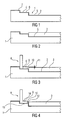
FIG. 1 shows a detail of a positioning device in cross section;
FIG. 2 shows a detail of the positioning device as shown in FIG. 1 with a placed-in covering glass in cross section;
FIG. 3 shows a detail of the positioning device as shown in FIG. 1 with a placed-in covering glass and a bonding frame in cross section;
FIG. 4 shows a detail of the positioning device as shown in FIG. 1 with a placed-in covering glass and a bonding frame and also a first adhesive in cross section;
FIG. 5 shows a detail of the positioning device as shown in FIG. 1 with a placed-in covering glass and a bonding frame and also a first adhesive and an introduced bonding mass in cross section;
FIG. 6 shows a detail of the positioning device as shown in FIG. 1 with a placed-in covering glass, a bonding frame, a liquid crystal display and a display module and also a first adhesive and an introduced bonding mass in cross section;
FIG. 7 shows a detail of the positioning device as shown in FIG. 1 with a placed-in covering glass, a bonding frame, a liquid crystal display and a display module and also a first and a second adhesive and an introduced bonding mass in cross section; and
FIG. 8 shows a detail of a display unit inserted into a recess of a display panel in cross section.
DETAILED DESCRIPTION OF THE PRESENTLY PREFERRED EMBODIMENTS
The positioning device 1 represented in FIG. 1 has a lower-lying first stepped recess 2, which corresponds in its peripheral contour to a covering glass 3 to be placed in and is open to one side. On the opening side of the first stepped recess 2, in the positioning device 1 there is formed a second stepped recess 4, the areal extent of which is greater than that of the first stepped recess 2, so that an offset in relation to the first stepped recess 2 is formed peripherally by the second stepped recess 4.
The bottom of the first stepped recess 2 forms a first contact surface 5 and the bottom of the second stepped recess 4 forms a second contact surface 6, parallel to the first contact surface 5.
The walls of the first and second stepped recesses 2 and 4 are provided with a nonstick coating 7.
In FIG. 2, the covering glass 3, which consists of a glass of low reflection and has an antiglare-antireflective coating on the front side, has been placed in.
As FIG. 3 shows, in the second stepped recess 4 there has subsequently been placed an L-shaped bonding frame 8, which lies with the outer side 15 of its first portion, extending parallel to the plane of the covering glass 3 and forming a leg 9, on the first contact surface 5 and is directed with its free end toward the covering glass. In this case, a distance that forms a groove 10 remains between the end face at the free end of the leg 9 and the radially peripheral end face of the covering glass 3.
The inner side 16 of the leg 9, parallel to the outer side 15 of the leg 9, extends in a plane that extends parallel to and at a certain distance 11 from the plane of the side of the covering glass 3 that is facing away from an observer.
In FIG. 4, the groove 10 has been filled with a first adhesive 12, and thus has connected the covering glass 3 to the bonding frame 8.
As FIG. 5 shows, the side of the covering glass 3 that is facing away from an observer has been covered with a layer of a defined volume of a transparent bonding mass 13 in such a way that its plane facing away from an observer extends in the same plane as the inner side 16 of the leg 9. The layer of the bonding mass 13 reaches beyond the first adhesive 12 up to the free end face of the leg 9.
The second portion 14 of the L-shaped bonding frame 8 extends away from the second contact surface 6 and is lying with its outer side 17 against the side wall 18 of the second stepped recess 4.
In the receptacle formed by the bonding frame 8 there has subsequently been inserted a structural unit comprising a liquid crystal display 20 and a display module 19. As FIG. 7 shows, the liquid crystal display 20 has a greater extent than the covering glass 3 and lies with its region 21 of its front side 22 that extends beyond the covering glass 3 on the inner side 16 of the leg 9. Otherwise, the liquid crystal display is lying with its front side, formed by a display glass, on the bonding mass 13.
The covering glass, the bonding mass 13 and the display glass of the liquid crystal display 20 have largely corresponding refractive indices.
The extent of the area region of the actively controllable region 23 of the liquid crystal display 20 corresponds to the area of the covering glass 3 and is in parallel congruence with the latter.
The display module 19 has a housing 24 and has been connected by a second adhesive 25 to the second portion 14 of the bonding frame 8 (FIG. 7), so that the display unit is then ready for fitting into a recess 26 of a display panel 27.
In the housing 24 of the display module 19 there are control electronics for controlling the actively controllable region 23 of the liquid crystal display 20 and a lighting unit for transilluminating the liquid crystal display 20.
The depth of the first stepped recess 4 corresponds to the thickness of the display panel 27 in its region enclosing the recess 26. As a result, the distance 28 between the plane of the outer side 15 of the leg 9 and the area of the covering glass 3 on the observer side also corresponds to the thickness of the display panel 27 in its region enclosing the recess 26, so that the plane of the area of the covering glass 3 on the observer side extends in the same plane as the area of the display panel 27 on the observer side.
Thus, while there have been shown and described and pointed out fundamental novel features of the invention as applied to a preferred embodiment thereof, it will be understood that various omissions and substitutions and changes in the form and details of the devices illustrated, and in their operation, may be made by those skilled in the art without departing from the spirit of the invention. For example, it is expressly intended that all combinations of those elements and/or method steps which perform substantially the same function in substantially the same way to achieve the same results are within the scope of the invention. Moreover, it should be recognized that structures and/or elements and/or method steps shown and/or described in connection with any disclosed form or embodiment of the invention may be incorporated in any other disclosed or described or suggested form or embodiment as a general matter of design choice. It is the intention, therefore, to be limited only as indicated by the scope of the claims appended hereto.