US9674465B2 - Non-visible illumination scheme - Google Patents
Non-visible illumination scheme Download PDFInfo
- Publication number
- US9674465B2 US9674465B2 US14/729,585 US201514729585A US9674465B2 US 9674465 B2 US9674465 B2 US 9674465B2 US 201514729585 A US201514729585 A US 201514729585A US 9674465 B2 US9674465 B2 US 9674465B2
- Authority
- US
- United States
- Prior art keywords
- region
- interest
- image
- image sensor
- source
- Prior art date
- Legal status (The legal status is an assumption and is not a legal conclusion. Google has not performed a legal analysis and makes no representation as to the accuracy of the status listed.)
- Active, expires
Links
- 238000005286 illumination Methods 0.000 title description 9
- 238000000034 method Methods 0.000 claims abstract description 47
- 238000005096 rolling process Methods 0.000 claims abstract description 36
- 230000005855 radiation Effects 0.000 claims abstract description 25
- 230000003595 spectral effect Effects 0.000 claims description 17
- 230000003213 activating effect Effects 0.000 claims 6
- 230000004913 activation Effects 0.000 claims 2
- 239000003086 colorant Substances 0.000 claims 1
- 238000010586 diagram Methods 0.000 description 8
- 239000002184 metal Substances 0.000 description 6
- 238000003384 imaging method Methods 0.000 description 5
- 230000035945 sensitivity Effects 0.000 description 5
- 238000001514 detection method Methods 0.000 description 4
- 230000000694 effects Effects 0.000 description 4
- 230000003247 decreasing effect Effects 0.000 description 3
- 230000009977 dual effect Effects 0.000 description 3
- 230000010354 integration Effects 0.000 description 3
- 230000002207 retinal effect Effects 0.000 description 3
- 238000001228 spectrum Methods 0.000 description 3
- 239000000758 substrate Substances 0.000 description 3
- 238000012795 verification Methods 0.000 description 3
- 239000000463 material Substances 0.000 description 2
- 238000012986 modification Methods 0.000 description 2
- 230000004048 modification Effects 0.000 description 2
- 238000004904 shortening Methods 0.000 description 2
- 241001428800 Cell fusing agent virus Species 0.000 description 1
- 241000593989 Scardinius erythrophthalmus Species 0.000 description 1
- 230000003321 amplification Effects 0.000 description 1
- 238000003491 array Methods 0.000 description 1
- 238000006243 chemical reaction Methods 0.000 description 1
- 230000000295 complement effect Effects 0.000 description 1
- 238000002474 experimental method Methods 0.000 description 1
- 230000007274 generation of a signal involved in cell-cell signaling Effects 0.000 description 1
- 208000036971 interstitial lung disease 2 Diseases 0.000 description 1
- 238000004519 manufacturing process Methods 0.000 description 1
- 229910044991 metal oxide Inorganic materials 0.000 description 1
- 150000004706 metal oxides Chemical class 0.000 description 1
- 230000007935 neutral effect Effects 0.000 description 1
- 238000003199 nucleic acid amplification method Methods 0.000 description 1
- 230000003287 optical effect Effects 0.000 description 1
- 238000012545 processing Methods 0.000 description 1
- 239000004065 semiconductor Substances 0.000 description 1
- 238000003860 storage Methods 0.000 description 1
- 239000013589 supplement Substances 0.000 description 1
- 238000010200 validation analysis Methods 0.000 description 1
- 210000003462 vein Anatomy 0.000 description 1
Images


Classifications
-
- H—ELECTRICITY
- H01—ELECTRIC ELEMENTS
- H01L—SEMICONDUCTOR DEVICES NOT COVERED BY CLASS H10
- H01L27/00—Devices consisting of a plurality of semiconductor or other solid-state components formed in or on a common substrate
- H01L27/14—Devices consisting of a plurality of semiconductor or other solid-state components formed in or on a common substrate including semiconductor components sensitive to infrared radiation, light, electromagnetic radiation of shorter wavelength or corpuscular radiation and specially adapted either for the conversion of the energy of such radiation into electrical energy or for the control of electrical energy by such radiation
- H01L27/144—Devices controlled by radiation
- H01L27/146—Imager structures
- H01L27/14643—Photodiode arrays; MOS imagers
- H01L27/14645—Colour imagers
-
- H—ELECTRICITY
- H04—ELECTRIC COMMUNICATION TECHNIQUE
- H04N—PICTORIAL COMMUNICATION, e.g. TELEVISION
- H04N23/00—Cameras or camera modules comprising electronic image sensors; Control thereof
- H04N23/10—Cameras or camera modules comprising electronic image sensors; Control thereof for generating image signals from different wavelengths
- H04N23/11—Cameras or camera modules comprising electronic image sensors; Control thereof for generating image signals from different wavelengths for generating image signals from visible and infrared light wavelengths
-
- H04N5/332—
-
- H—ELECTRICITY
- H04—ELECTRIC COMMUNICATION TECHNIQUE
- H04N—PICTORIAL COMMUNICATION, e.g. TELEVISION
- H04N23/00—Cameras or camera modules comprising electronic image sensors; Control thereof
- H04N23/70—Circuitry for compensating brightness variation in the scene
- H04N23/741—Circuitry for compensating brightness variation in the scene by increasing the dynamic range of the image compared to the dynamic range of the electronic image sensors
-
- H—ELECTRICITY
- H01—ELECTRIC ELEMENTS
- H01L—SEMICONDUCTOR DEVICES NOT COVERED BY CLASS H10
- H01L27/00—Devices consisting of a plurality of semiconductor or other solid-state components formed in or on a common substrate
- H01L27/14—Devices consisting of a plurality of semiconductor or other solid-state components formed in or on a common substrate including semiconductor components sensitive to infrared radiation, light, electromagnetic radiation of shorter wavelength or corpuscular radiation and specially adapted either for the conversion of the energy of such radiation into electrical energy or for the control of electrical energy by such radiation
- H01L27/144—Devices controlled by radiation
- H01L27/146—Imager structures
- H01L27/14601—Structural or functional details thereof
- H01L27/1464—Back illuminated imager structures
-
- H—ELECTRICITY
- H04—ELECTRIC COMMUNICATION TECHNIQUE
- H04N—PICTORIAL COMMUNICATION, e.g. TELEVISION
- H04N23/00—Cameras or camera modules comprising electronic image sensors; Control thereof
- H04N23/56—Cameras or camera modules comprising electronic image sensors; Control thereof provided with illuminating means
-
- H—ELECTRICITY
- H04—ELECTRIC COMMUNICATION TECHNIQUE
- H04N—PICTORIAL COMMUNICATION, e.g. TELEVISION
- H04N23/00—Cameras or camera modules comprising electronic image sensors; Control thereof
- H04N23/70—Circuitry for compensating brightness variation in the scene
- H04N23/72—Combination of two or more compensation controls
-
- H—ELECTRICITY
- H04—ELECTRIC COMMUNICATION TECHNIQUE
- H04N—PICTORIAL COMMUNICATION, e.g. TELEVISION
- H04N25/00—Circuitry of solid-state image sensors [SSIS]; Control thereof
- H04N25/10—Circuitry of solid-state image sensors [SSIS]; Control thereof for transforming different wavelengths into image signals
- H04N25/11—Arrangement of colour filter arrays [CFA]; Filter mosaics
- H04N25/13—Arrangement of colour filter arrays [CFA]; Filter mosaics characterised by the spectral characteristics of the filter elements
- H04N25/131—Arrangement of colour filter arrays [CFA]; Filter mosaics characterised by the spectral characteristics of the filter elements including elements passing infrared wavelengths
-
- H—ELECTRICITY
- H04—ELECTRIC COMMUNICATION TECHNIQUE
- H04N—PICTORIAL COMMUNICATION, e.g. TELEVISION
- H04N25/00—Circuitry of solid-state image sensors [SSIS]; Control thereof
- H04N25/10—Circuitry of solid-state image sensors [SSIS]; Control thereof for transforming different wavelengths into image signals
- H04N25/11—Arrangement of colour filter arrays [CFA]; Filter mosaics
- H04N25/13—Arrangement of colour filter arrays [CFA]; Filter mosaics characterised by the spectral characteristics of the filter elements
- H04N25/133—Arrangement of colour filter arrays [CFA]; Filter mosaics characterised by the spectral characteristics of the filter elements including elements passing panchromatic light, e.g. filters passing white light
-
- H—ELECTRICITY
- H04—ELECTRIC COMMUNICATION TECHNIQUE
- H04N—PICTORIAL COMMUNICATION, e.g. TELEVISION
- H04N25/00—Circuitry of solid-state image sensors [SSIS]; Control thereof
- H04N25/10—Circuitry of solid-state image sensors [SSIS]; Control thereof for transforming different wavelengths into image signals
- H04N25/11—Arrangement of colour filter arrays [CFA]; Filter mosaics
- H04N25/13—Arrangement of colour filter arrays [CFA]; Filter mosaics characterised by the spectral characteristics of the filter elements
- H04N25/135—Arrangement of colour filter arrays [CFA]; Filter mosaics characterised by the spectral characteristics of the filter elements based on four or more different wavelength filter elements
-
- H—ELECTRICITY
- H04—ELECTRIC COMMUNICATION TECHNIQUE
- H04N—PICTORIAL COMMUNICATION, e.g. TELEVISION
- H04N25/00—Circuitry of solid-state image sensors [SSIS]; Control thereof
- H04N25/50—Control of the SSIS exposure
- H04N25/53—Control of the integration time
- H04N25/531—Control of the integration time by controlling rolling shutters in CMOS SSIS
-
- H—ELECTRICITY
- H04—ELECTRIC COMMUNICATION TECHNIQUE
- H04N—PICTORIAL COMMUNICATION, e.g. TELEVISION
- H04N25/00—Circuitry of solid-state image sensors [SSIS]; Control thereof
- H04N25/60—Noise processing, e.g. detecting, correcting, reducing or removing noise
- H04N25/62—Detection or reduction of noise due to excess charges produced by the exposure, e.g. smear, blooming, ghost image, crosstalk or leakage between pixels
-
- H—ELECTRICITY
- H04—ELECTRIC COMMUNICATION TECHNIQUE
- H04N—PICTORIAL COMMUNICATION, e.g. TELEVISION
- H04N25/00—Circuitry of solid-state image sensors [SSIS]; Control thereof
- H04N25/70—SSIS architectures; Circuits associated therewith
-
- H—ELECTRICITY
- H04—ELECTRIC COMMUNICATION TECHNIQUE
- H04N—PICTORIAL COMMUNICATION, e.g. TELEVISION
- H04N25/00—Circuitry of solid-state image sensors [SSIS]; Control thereof
- H04N25/70—SSIS architectures; Circuits associated therewith
- H04N25/71—Charge-coupled device [CCD] sensors; Charge-transfer registers specially adapted for CCD sensors
- H04N25/75—Circuitry for providing, modifying or processing image signals from the pixel array
-
- H—ELECTRICITY
- H04—ELECTRIC COMMUNICATION TECHNIQUE
- H04N—PICTORIAL COMMUNICATION, e.g. TELEVISION
- H04N25/00—Circuitry of solid-state image sensors [SSIS]; Control thereof
- H04N25/70—SSIS architectures; Circuits associated therewith
- H04N25/76—Addressed sensors, e.g. MOS or CMOS sensors
-
- H04N5/2256—
-
- H04N5/2352—
-
- H04N5/3532—
-
- H04N5/374—
-
- H04N9/045—
Definitions
- the disclosed embodiments relate generally to digital photography and in particular, but not exclusively, to an illumination scheme that improves imaging at with non-visible wavelengths while decreasing power consumption.
- Cameras are incorporated into many kinds of mobile devices such as cell phones, smart phones tablets and the like so much that nowadays virtually every mobile device includes a camera. Initially the camera's function was simply to take pictures, but many cameras are now also used for additional functions such as user identification and validation, gesture recognition, and so on. For various reasons many of these additional functions must be carried out using non-visible (i.e., invisible) light such as infrared, and so the mobile devices must also include some kind of radiation (i.e., light) source that provides the needed non-visible radiation.
- non-visible light i.e., invisible
- the mobile devices must also include some kind of radiation (i.e., light) source that provides the needed non-visible radiation.
- FIGS. 1A-1B are perspective and cross-sectional drawings of an embodiment of an image capture device including non-visible lighting.
- FIG. 2A is a schematic of an embodiment of an image sensor including a color filter array
- FIGS. 2B-2C are, respectively, cross-sections of embodiments of a pair of frontside-illuminated pixels and embodiments of a pair of backside-illuminated pixels.
- FIGS. 3A-3B are, respectively, a diagram of an embodiment of a color filter array (CFA) formed by tiling multiple minimal repeating units (MRUs) and a diagram of a pair of embodiments of an MRU.
- CFA color filter array
- MRUs multiple minimal repeating units
- FIG. 4 is a diagram illustrating an embodiment of the operation of a rolling shutter in an image sensor.
- FIG. 5 is a diagram of an embodiment of an image frame including a region of interest within the frame.
- FIG. 6 is a flowchart illustrating an embodiment of a process for improved non-visible illumination and image capture.
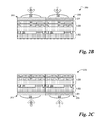
- FIGS. 7A-7B are diagrams illustrating an embodiment of exposure time adjustment.
- FIG. 8 is a timing diagram illustrating an embodiment of the timing of various events during capturing an image of a region of interest with a non-visible wavelength of light.
- Embodiments are described of an apparatus, system and method for a non-visible illumination scheme that improves image capture while decreasing power consumption. Specific details are described to provide a thorough understanding of the embodiments, but one skilled in the relevant art will recognize that the invention can be practiced without one or more of the described details, or with other methods, components, materials, etc. In some instances, well-known structures, materials, or operations are not shown or described in detail but are nonetheless encompassed within the scope of the invention.
- FIGS. 1A-1B together illustrate an embodiment of an image capture device 100 .
- the illustrated embodiment of device 100 is a camera, but in other embodiments device 100 can be any device that includes an image sensor, such as a mobile phone, smart phone, template, laptop etc.
- Device 100 includes optics 102 for focusing an image of an object 104 onto an image sensor 112 within the device.
- image sensor 112 can be a CMOS image sensor such as the ones shown in FIGS. 2A-2C , but in other embodiments can be another type of image sensor.
- Object 104 can be illuminated by different light sources. It can be illuminated by an external light source 106 which keep it can be natural light (i.e., sunlight) if object 104 is outdoors or artificial light if object 104 is indoors. If external light source 106 is to dim to properly illuminate object 104 , an onboard visible light source 108 mounted on or in device 100 can replace or supplement external light source 106 to illuminate object 104 .
- non-visible light source 110 can be used to illuminate object 104 with non-visible radiation for special imaging situations.
- non-visible light source 110 can be an infrared light source, but in other embodiments can be a non-visible light source that emits at another wavelength such as ultraviolet.
- non-visible light source 110 can be used for special imaging situations such as identity verification.
- identity verification In a smartphone, for instance, non-visible wavelengths can be used to perform a retinal scan to verify that the person trying to use the smart phone is its rightful owner.
- on-visible light source 110 is not limited to this particular application. Other applications for which it could be used include iris recognition, vein recognition, gesture detection, motion detection, face detection, proximity detection, and so on.
- all or part of object 104 is illuminated by one or both of external light source 106 or onboard visible light source 108 for normal (i.e., visible) imaging. And if a situation requiring non-visible light source 110 is present, all or part of object 104 can be illuminated with non-visible light source 110 .
- light incident on object 104 from a source reflects from the object and is focused by optics 102 onto image sensor 112 .
- Image sensor 112 has an exposure cycle during which it captures the light focused on it by optics 102 and generates electric signals that then form the basis of a digital image of object 104 .
- non-visible light source 110 when non-visible light source 110 is used it stays on during the entire exposure cycle of the image sensor, even if it is only needed to capture an image of part of the object. For instance, identity verification using a retinal scan needs only an image of the eyes, not an image of the entire person or even the entire face. But light sources like non-visible light source 110 can use a significant amount of power, and that can be a problem in devices that have power constraints—for instance, devices that operate using batteries. The embodiments described below reduce this problem by using a smart illumination scheme for non-visible light source 110 .
- FIG. 2A illustrates an embodiment of a complementary metal oxide semiconductor (CMOS) image sensor 200 including a color pixel array 205 , readout circuitry 270 coupled to the pixel array, function logic 215 coupled to the readout circuitry, and control circuitry 220 coupled to the pixel array.
- Color pixel array 205 is a two-dimensional (“2D”) array of individual imaging sensors or pixels (e.g., pixels P 1 , P 2 . . . , Pn) having X pixel columns and Y pixel rows.
- Color pixel array 205 can be implemented as a frontside-illuminated image sensor, as shown in FIG. 2A , or as a backside-illuminated image sensor, as shown in FIG. 2B .
- each pixel in the array is arranged into a row (e.g., rows R 1 to Ry) and a column (e.g., column C 1 to Cx) to acquire image data of a person, place, or object, which can then be used to render a 2D image of the person, place, or object.
- Color pixel array 205 assigns color to each pixel using a color filter array (CFA) coupled to the pixel array, as further discussed below in connection with the disclosed embodiments of color filter arrays.
- CFA color filter array
- Readout circuitry 270 can include amplification circuitry, analog-to-digital (“ADC”) conversion circuitry, or other circuits.
- Function logic 215 can store the image data and/or manipulate the image data by applying post-image effects (e.g., crop, rotate, remove red eye, adjust brightness, adjust contrast, or otherwise). Function logic 215 can also be used in one embodiment to process the image data to correct (i.e., reduce or remove) fixed pattern noise.
- Control circuitry 220 is coupled to pixel array 205 to control operational characteristic of color pixel array 205 . For example, control circuitry 220 can generate a shutter signal for controlling image acquisition.
- FIG. 2B illustrates a cross-section of an embodiment of a pair of frontside-illuminated (FSI) pixels 250 in a CMOS image sensor.
- the front side of FSI pixels 250 is the side of substrate 202 upon which the photosensitive area 204 and associated pixel circuitry are disposed, and over which metal stack 206 for redistributing signals is formed.
- Metal stack 206 includes metal layers M 1 and M 2 , which are patterned to create an optical passage through which light incident on FSI pixels 250 can reach photosensitive or photodiode (“PD”) regions 204 .
- PD photosensitive or photodiode
- the front side can include color filter array 201 , with each of its individual color filters (only two individual filters 203 and 205 are illustrated in this particular cross section) disposed under a microlens 206 that aids in focusing incident light onto PD region 204 .
- color filter array 201 can be a color filter array formed with any of the minimal repeating units and filters described in FIGS. 3A-3B .
- FIG. 2C illustrates a cross-section of an embodiment of a pair of backside-illuminated (BSI) pixels 275 in a CMOS image sensor.
- BSI pixels 250 the front side of pixels 275 is the side of substrate 202 upon which the photosensitive regions 204 and associated pixel circuitry are disposed, and over which metal stack 206 is formed for redistributing signals.
- the backside is the side of substrate 202 opposite the front side.
- the backside can include color filter array 201 , with each of its individual color filters (individual filters 203 and 205 are illustrated in this particular cross section) disposed under a microlens 206 .
- color filter array 201 can be a color filter array formed with any of the minimal repeating units and filters described in FIGS. 3A-3B .
- Microlenses 206 aid in focusing incident light onto photosensitive regions 204 .
- Backside illumination of pixels 275 means that the metal interconnect lines in metal stack 206 do not obscure the path between the object being imaged and the photosensitive regions 204 , resulting in greater signal generation by photosensitive regions 204 .
- FIG. 3A illustrates a color filter array (CFA) 300 including a plurality of minimal repeating units (MRUs) that are tiled to form the CFA.
- CFA 300 includes a number of individual filters that substantially corresponds to the number of individual pixels in the pixel array to which the CFA is or will be coupled. Each individual filter is optically coupled to a corresponding individual pixel in the pixel array and has a particular spectral photoresponse selected from a set of spectral photoresponses. A particular spectral photoresponse has high sensitivity to certain portions of the electromagnetic spectrum but low sensitivity to other portions of the spectrum.
- a pixel can be referred to as a “clear pixel” if it has no filter or is coupled to a clear (i.e., colorless or panchromatic) filter, as a “blue pixel” if it is coupled to a blue filter, as a “green pixel” if it is coupled to a green filter, or as a “red pixel” if it is coupled to a red filter, and so on.
- the set of spectral photoresponses selected for use in a CFA usually has at least three different photoresponses, but in some embodiments can include four or more.
- the set of photoresponses can be red, green, blue, and clear or panchromatic (i.e., neutral or colorless).
- CFA 300 can include other photoresponses in addition to, or instead of, those listed.
- other embodiments can include cyan (C), magenta (M), and yellow (Y) filters, clear (i.e., colorless) filters, infrared filters, ultraviolet filters, x-ray filters, etc.
- Multi-band filters which have high sensitivity to multiple parts of the electromagnetic spectrum, can also be used in some embodiments.
- CFA 300 The individual filters in CFA 300 are grouped into minimal repeating units (MRUs) such as MRU 302 , and MRUs 302 are then tiled vertically and horizontally, as indicated by the arrows, to form CFA 300 .
- MRUs minimal repeating units
- a minimal repeating unit is a repeating unit such that no other repeating unit has fewer individual filters.
- a color filter array can include several different repeating units, but a repeating unit is not a minimal repeating unit if there is another repeating unit in the array with fewer individual filters.
- Other embodiments of CFA 300 can be tiled using an MRU that includes a greater or smaller number of pixels than illustrated for MRU 302 .
- FIG. 3B illustrates embodiments of a minimal repeating unit (MRU) 302 .
- the four individual filters within MRU 302 include three dual-band filters and one single-band filter.
- the dual-band filters as their name implies, have spectral photoresponses that allow them to filter two different electromagnetic wavelength bands.
- the dual-band filters each filter a visible wavelength (e.g., red, blue, and green) and a non-visible wavelength (e.g., infrared (IR), and near infrared (NIR)) while the single-band filter filters the non-visible wavelength.
- IR infrared
- NIR near infrared
- This arrangement of dual-band filters and a single-band filter where the single-band filter's band matches the non-visible band of the dual-band filter allows any image sensor to which color filter array 300 is optically coupled to capture full-resolution images at the non-visible wavelength, instead of the quarter-resolution images that would be captured if only single-band filters were used in the color filter array.
- the dual-band filters have infrared as their non-visible wavelength and have red (R), green (G), and blue (B) as their visible wavelength.
- the embodiment shown on the right is similar except that it uses a different primary color set. Instead of the RGB color set, the embodiment on the left uses the cyan-magenta-yellow (CMY) color set for the visible wavelengths filtered by the dual-band filters.
- the single-band filter is an infrared filter, so that the non-visible wavelengths filtered by the dual-band filters are substantially the same as the non-visible wavelengths filtered by the one single-band filter.
- FIG. 4 illustrates an embodiment of operation of a rolling shutter generally found in CMOS image sensors.
- a rolling shutter is not a mechanical device that opens and closes to expose the image sensor to light. It is instead a procedure for exposing and reading pixels in a CMOS image sensor.
- light exposure starts and ends at different times for different rows of pixels.
- First row R 1 is subjected to a reset, then automatically exposed to light; thus integration (production of photoelectric charges) starts immediately after reset.
- the exposure time i.e., the exposure time
- the second row is then reset and starts light exposure and integration at a predetermined time after the first row is reset; but the second row readout commences readout only after the first row readout is finished, because the image sensor can only read out one row of pixels at a time.
- This reset, integration, and signal readout process is done row by row in the image sensor, from first row R 1 to last row Ry, to produce a full image frame.
- the rolling shutter causes each frame captured to appear as a parallelogram because of the way the rolling shutter captures each subsequent row slightly later than the previous row.
- an image sensor usually uses its rolling shutter to capture multiple frames before producing a final output (see, e.g., FIG. 8 ).
- Many of the early frames captured are used for other purposes, such as exposure adjustment or focus adjustment, then discarded before or when the final image is captures or output.
- FIG. 5 illustrates an embodiment of an image frame 500 of object 503 that can be captured using a rolling shutter.
- the rolling shutter starts at top row R 1 and scans down through Ry in the procedure shown in FIG. 4 .
- Frame 500 includes a region of interest (ROI) 502 that extends vertically between row Ri and row Rj, and has a height, measured in rows, of ⁇ R. Also within frame 500 are an upper region 504 and a lower region 506 that are within frame 500 but outside ROI 502 : upper region 504 extends from the top of the frame to where ROI 502 begins at row Ri, while lower region 506 extends from where ROI 502 ends at row Rj to the bottom of frame 500 .
- ROI region of interest
- the position of ROI 502 within frame 500 is determined based upon one or more previous visible-light frames of object 503 .
- ROI 502 includes the features of object 503 that are to be imaged with non-visible light.
- object 503 is a person's face and ROI 502 encompasses the person's eyes; this embodiment can be useful, for instance, for identity verification using a retinal scan.
- ROI 502 includes not only the person's eyes, but also a 10% margin above and below the eyes to ensure a full coverage of the eyes. But in other embodiments the object and region of interest can of course be different depending on the application.
- FIG. 6 illustrates an embodiment of a process 600 for providing efficient non-visible lighting during capture of an image of a region of interest (ROI) (see FIG. 5 ) by image capture device 100 using a color filter array such as CFA 300 with MRU 302 .
- the process starts at block 602 .
- one or more full-resolution frames of the object are captured at visible wavelengths using an external light source or an onboard visible light source (see FIGS. 1A-1B ).
- the full-resolution frames captured at block 604 are used to determine the region of interest within the frame, for instance using feature recognition software.
- the process determines an adjusted exposure time that will substantially reduce or eliminate the amount of visible light captured by the image sensor. If necessary the process can continue to block 610 , which has a dashed outline to indicate that it is optional, where additional image frames at visible wavelengths can be captured and used to determine the adjusted exposure time. In one embodiment the process at block 610 can capture multiple frames at decreasing exposure times and use the captured frames to extrapolate the required adjusted exposure time. But in other embodiments the adjusted exposure time can be determined differently. After determining the adjusted exposure time, which is inversely related to the image sensor's frame rate (exposure time ⁇ 1/frame rate), the process sets the exposure time of the image sensor to the adjusted exposure time. In one embodiment the image sensor's exposure time can be set by adjusting the vertical blanking period, but in other embodiments it can be set differently, for instance by adjusting the sensor's frame rate.
- the process determines a delay for the non-visible light source.
- the delay substantially corresponds to the time from when the rolling shutters starts scanning the frame at row R 1 until it reaches row Ri, which marks the beginning of the ROI 502 .
- the delay depends on the value of Ri—or, put differently, on the position of ROI 502 within frame 500 —as well as on the adjusted exposure time set at block 608 .
- the process determines and sets the intensity and pulse duration of the non-visible light source.
- the intensity depends on factors such as the adjusted exposure time; the adjusted exposure time is typically made short to exclude as much visible light as possible, but the short exposure time can require a higher-intensity non-visible pulse than might otherwise be required.
- the duration of the non-visible pulse depends on the amount of time it takes the rolling shutter to traverse pixel rows within the ROI, which in turn depends on the exposure time and the dimensions of the ROI. In FIG. 5 , for instance, the duration of the non-visible light pulse depends on the adjusted exposure time as well as on AR, the height in rows of ROI 502 .
- the process starts the rolling shutter at the beginning of frame 500 .
- the process checks whether the delay has expired. If at block 618 the delay has not expired, it means the rolling shutter is still in region 504 and has not reached ROI 502 , so the process continues to block 620 where the rolling shutter keeps on capturing rows of the image frame. But if at block 618 the delay has expired, it means the rolling shutter has reached ROI 502 and the process continues to block 622 , where it activates the non-visible light source at the determined intensity.
- the process checks whether the non-visible light source has been on for the determined duration. If at block 624 the non-visible light source has not been on for the duration, it means the rolling shutter is still within ROI 502 and the process returns to block 622 , where it keeps the non-visible light source activated at the determined intensity. But if at block 624 the non-visible light source has been on for the determined duration, it means the rolling shutter has reached the end of ROI 502 and is about to enter region 506 where the non-visible light source is no longer needed. Because the delay has expired, the process continues to block 626 where it deactivates the non-visible light source.
- the process determines whether an acceptable image of the ROI was captured.
- the captured image of the ROI will be a full-resolution image because of the use of dual band filters, but it is possible that not every combination of delay, duration, and intensity will produce an acceptable image. If at block 628 the process determines that an acceptable image was captured the process continues to block 430 were it stops. But if at block 628 the process determines that an acceptable image was not captured then it proceeds to block 632 .
- At block 632 to the process determines if the ROI needs to be updated, for instance because object 503 has moved relative to frame 500 . If at block 632 the process determines that an ROI update is needed, the process returns to block 604 and goes through the remainder of process 600 . But if at block 632 the process determines that no ROI update is needed, it returns to block 608 and goes through the remainder of process 600 .
- FIGS. 7A-7B illustrate an embodiment of the effect of exposure adjustment on an image frame.
- FIG. 7A shows a parallelogram representing a single frame, as discussed above for FIG. 4 .
- the length of a side along the time axis represents the exposure time E of the frame.
- FIG. 7B shows the effect of shortening the exposure time to eliminate or substantially reduce visible light.
- the net effect of shortening the exposure time is to substantially reduce the width of the parallelogram.
- the number of rows in the ROI remains constant, but because the parallelogram is narrowed an image of ROI 502 can be captured much more quickly, and with a shorter non-visible illumination pulse, while excluding most or all visible light that can interfere with the capture of a non-visible ROI image.
- the exposure time is controlled so that the image signal generated by visible light is one tenth of the image signal generated by non-visible IR light, or less. Since dual band filters generate photoelectric image signals caused by both visible light and non-visible IR light, too much visible light will cause significant noise to the desired IR image for applications such as iris recognition of the eyes. In particular, for the visible light (e.g., red, blue and green) channels, a visible light noise that is more than 10% of the IR signal may be deemed excessive. Accordingly, the exposure time for IR image generation is set to a level such that the signal to noise ratio is 10:1, or more.
- ambient light source that includes a high level of IR (e.g., outdoor lighting under the sun) means a relatively small amount of visible light noise and a relatively large amount of IR signal, while certain types of indoor fluorescent light (e.g., compact fluorescent light) is mostly in the visible range, thereby causing a relatively high amount of visible light noise.
- indoor fluorescent light e.g., compact fluorescent light
- a high wattage of the non-visible IR LED light source increases the IR signal to visible noise ratio.
- the distance between the non-visible IR LED light source and the object affects the amount of non-visible IR light upon the object, following an inverse square relationship (i.e., power is inversely proportional to the square of the distance).
- a longer duration of the non-visible IR radiation e.g., non-visible IR LED pulse
- a shorter exposure time of image sensor pixels that include dual band visible plus non-visible IR pixels reduces the noise caused by visible light. In addition to the above five factors, several other factors should also be considered.
- pixel's inherent sensitivity to IR e.g., front side illumination, or FSI sensors tend to have lower IR sensitivity than back side illumination, or BSI sensors
- pixel's inherent sensitivity to IR e.g., pixel size (e.g., larger pixel is more sensitive to IR), etc.
- IR LED when IR LED is pulse flashed for 0.5 ms, a pixel exposure time of 8 ms yields an unsatisfactory result of IR signal to visible noise ratio of less than 10.
- the pixel exposure time is reduced to 2.5 ms, the IR signal to visible noise ratio reaches a satisfactory level of over ten.
- FIG. 8 illustrates an embodiment of a timing diagram for functions that implement process 600 .
- the horizontal axis at the top represents time and hence the lines below the horizontal axis illustrate the timing of five different functions used in an implementation of process 600 .
- the illustrated timings are of the vertical blanking period, the exposure, the data output, the assertion of the strobe request, and the strobe pulse.
- the first row shows the timing of the vertical blanking period.
- a vertical blanking period also known as a vertical blanking interval, is the time between when the rolling shutter finishes capture of the final line of a frame and when it starts capture of the first line of the next frame.
- the vertical blanking period can be used to adjust the exposure time of an image frame; for a given frame rate, a longer blanking period means a shorter exposure.
- the second row illustrates the exposure—in this case, the capture of multiple image frames.
- each parallelogram 801 through 805 is an image frame, meaning that some of several image frames are captured. As explained above, one or more early flame frames are used for functions such as exposure time adjustment and then discarded.
- the fourth complete frame 804 is used for capture of the ROI image, although other embodiments can use a different frame for the capture of the ROI image.
- the third row of FIG. 8 shows the timing of the data output (i.e., output of the image data from each captured frame).
- the fourth row shows the assertion of the strobe request.
- the strobe request is asserted in an earlier frame and de-asserted after capture of the non-visible image of the ROI.
- the fifth and final row shows the timing of the strobe pulls; as discussed above, the strobe pulls happens during exposure by the rolling shutter of the ROI as discussed above.
Priority Applications (3)
| Application Number | Priority Date | Filing Date | Title |
|---|---|---|---|
| US14/729,585 US9674465B2 (en) | 2015-06-03 | 2015-06-03 | Non-visible illumination scheme |
| CN201610323185.9A CN106254785B (zh) | 2015-06-03 | 2016-05-16 | 图像传感器及用于改进非可见照明的方法 |
| TW105117453A TWI612371B (zh) | 2015-06-03 | 2016-06-02 | 影像感測器及影像擷取程序 |
Applications Claiming Priority (1)
| Application Number | Priority Date | Filing Date | Title |
|---|---|---|---|
| US14/729,585 US9674465B2 (en) | 2015-06-03 | 2015-06-03 | Non-visible illumination scheme |
Publications (2)
| Publication Number | Publication Date |
|---|---|
| US20160360124A1 US20160360124A1 (en) | 2016-12-08 |
| US9674465B2 true US9674465B2 (en) | 2017-06-06 |
Family
ID=57452652
Family Applications (1)
| Application Number | Title | Priority Date | Filing Date |
|---|---|---|---|
| US14/729,585 Active 2035-07-14 US9674465B2 (en) | 2015-06-03 | 2015-06-03 | Non-visible illumination scheme |
Country Status (3)
| Country | Link |
|---|---|
| US (1) | US9674465B2 (zh) |
| CN (1) | CN106254785B (zh) |
| TW (1) | TWI612371B (zh) |
Cited By (1)
| Publication number | Priority date | Publication date | Assignee | Title |
|---|---|---|---|---|
| US11527053B2 (en) | 2018-12-12 | 2022-12-13 | Samsung Electronics Co., Ltd. | Method and apparatus of processing image |
Families Citing this family (13)
| Publication number | Priority date | Publication date | Assignee | Title |
|---|---|---|---|---|
| US20170061210A1 (en) * | 2015-08-26 | 2017-03-02 | Intel Corporation | Infrared lamp control for use with iris recognition authentication |
| US10699147B2 (en) * | 2017-06-22 | 2020-06-30 | BITO Robotics, Inc. | Systems and methods for fast identification and processing of an image area of interest |
| CN107205126B (zh) * | 2017-06-30 | 2020-04-24 | 联想(北京)有限公司 | 一种控制方法及处理装置 |
| TWI630556B (zh) * | 2017-07-26 | 2018-07-21 | 聚晶半導體股份有限公司 | 影像擷取裝置及其紅外線感測方法 |
| US11280908B2 (en) * | 2017-08-15 | 2022-03-22 | Black Sesame Technologies Inc. | Obstacle detection by global shutter image sensor |
| US10771766B2 (en) * | 2018-03-30 | 2020-09-08 | Mediatek Inc. | Method and apparatus for active stereo vision |
| FR3091114B1 (fr) * | 2018-12-19 | 2021-06-11 | Valeo Comfort & Driving Assistance | dispositif de capture d’images et système de surveillance d’un conducteur associé |
| WO2020237482A1 (zh) * | 2019-05-27 | 2020-12-03 | 深圳市汇顶科技股份有限公司 | 用于人脸识别的光学传感器、装置、方法和电子设备 |
| CN112036222B (zh) * | 2019-06-04 | 2023-12-29 | 星宸科技股份有限公司 | 脸部辨识系统及方法 |
| CN111611952B (zh) * | 2020-05-27 | 2023-07-14 | 深圳市汇顶科技股份有限公司 | 指纹识别装置和电子设备 |
| CN115917297A (zh) * | 2020-05-29 | 2023-04-04 | 奎多公司 | 用于疾病诊断的样本测定的远程评估的系统和方法 |
| CN114257712A (zh) * | 2020-09-25 | 2022-03-29 | 华为技术有限公司 | 控制摄像头模组补光时间的方法及装置 |
| CN114697474B (zh) * | 2020-12-25 | 2023-07-21 | Oppo广东移动通信有限公司 | 电子设备的控制方法、电子设备及计算机可读存储介质 |
Citations (8)
| Publication number | Priority date | Publication date | Assignee | Title |
|---|---|---|---|---|
| US6239840B1 (en) * | 1996-12-25 | 2001-05-29 | Matsushita Electric Industrial Co., Ltd. | Exposure controller having coring value adapted to the discharge pulse count |
| US6292212B1 (en) * | 1994-12-23 | 2001-09-18 | Eastman Kodak Company | Electronic color infrared camera |
| US20070221849A1 (en) * | 2005-07-12 | 2007-09-27 | Northrop Grumman Corporation | Infrared laser illuminated imaging systems and methods |
| US20110260059A1 (en) * | 2010-04-21 | 2011-10-27 | Sionyx, Inc. | Photosensitive imaging devices and associated methods |
| US20110298886A1 (en) * | 2010-06-06 | 2011-12-08 | Apple, Inc. | Auto Exposure Techniques for Variable Lighting Conditions |
| US20110304614A1 (en) | 2010-06-11 | 2011-12-15 | Sony Corporation | Stereoscopic image display device and stereoscopic image display method |
| US8446470B2 (en) | 2007-10-04 | 2013-05-21 | Magna Electronics, Inc. | Combined RGB and IR imaging sensor |
| US20140160253A1 (en) | 2012-12-10 | 2014-06-12 | Microsoft Corporation | Hyperspectral imager |
Family Cites Families (5)
| Publication number | Priority date | Publication date | Assignee | Title |
|---|---|---|---|---|
| US20100148291A1 (en) * | 2008-12-15 | 2010-06-17 | Tivarus Cristian A | Ultraviolet light filter layer in image sensors |
| US8947572B2 (en) * | 2010-05-24 | 2015-02-03 | Omnivision Technologies, Inc. | Dual-sided image sensor |
| US9692992B2 (en) * | 2013-07-01 | 2017-06-27 | Omnivision Technologies, Inc. | Color and infrared filter array patterns to reduce color aliasing |
| TW201514599A (zh) * | 2013-10-07 | 2015-04-16 | Novatek Microelectronics Corp | 影像感測器及影像擷取系統 |
| CN103902390B (zh) * | 2014-03-12 | 2017-04-19 | 深圳创维-Rgb电子有限公司 | 基于Android的应用层的进程间通信方法及基础应用通信系统 |
-
2015
- 2015-06-03 US US14/729,585 patent/US9674465B2/en active Active
-
2016
- 2016-05-16 CN CN201610323185.9A patent/CN106254785B/zh active Active
- 2016-06-02 TW TW105117453A patent/TWI612371B/zh active
Patent Citations (8)
| Publication number | Priority date | Publication date | Assignee | Title |
|---|---|---|---|---|
| US6292212B1 (en) * | 1994-12-23 | 2001-09-18 | Eastman Kodak Company | Electronic color infrared camera |
| US6239840B1 (en) * | 1996-12-25 | 2001-05-29 | Matsushita Electric Industrial Co., Ltd. | Exposure controller having coring value adapted to the discharge pulse count |
| US20070221849A1 (en) * | 2005-07-12 | 2007-09-27 | Northrop Grumman Corporation | Infrared laser illuminated imaging systems and methods |
| US8446470B2 (en) | 2007-10-04 | 2013-05-21 | Magna Electronics, Inc. | Combined RGB and IR imaging sensor |
| US20110260059A1 (en) * | 2010-04-21 | 2011-10-27 | Sionyx, Inc. | Photosensitive imaging devices and associated methods |
| US20110298886A1 (en) * | 2010-06-06 | 2011-12-08 | Apple, Inc. | Auto Exposure Techniques for Variable Lighting Conditions |
| US20110304614A1 (en) | 2010-06-11 | 2011-12-15 | Sony Corporation | Stereoscopic image display device and stereoscopic image display method |
| US20140160253A1 (en) | 2012-12-10 | 2014-06-12 | Microsoft Corporation | Hyperspectral imager |
Non-Patent Citations (2)
| Title |
|---|
| ROC (Taiwan) Pat. Appl. No. 105117453-First Office Action with English Translation mailed Feb. 3, 2017, 13 pages. |
| ROC (Taiwan) Pat. Appl. No. 105117453—First Office Action with English Translation mailed Feb. 3, 2017, 13 pages. |
Cited By (2)
| Publication number | Priority date | Publication date | Assignee | Title |
|---|---|---|---|---|
| US11527053B2 (en) | 2018-12-12 | 2022-12-13 | Samsung Electronics Co., Ltd. | Method and apparatus of processing image |
| US11830234B2 (en) | 2018-12-12 | 2023-11-28 | Samsung Electronics Co., Ltd. | Method and apparatus of processing image |
Also Published As
| Publication number | Publication date |
|---|---|
| TWI612371B (zh) | 2018-01-21 |
| TW201716849A (zh) | 2017-05-16 |
| CN106254785A (zh) | 2016-12-21 |
| CN106254785B (zh) | 2019-05-17 |
| US20160360124A1 (en) | 2016-12-08 |
Similar Documents
| Publication | Publication Date | Title |
|---|---|---|
| US9674465B2 (en) | Non-visible illumination scheme | |
| US9521381B2 (en) | RGBC color filter array patterns to minimize color aliasing | |
| US8405748B2 (en) | CMOS image sensor with improved photodiode area allocation | |
| US9756298B2 (en) | Color filter array with reference pixel to reduce spectral crosstalk | |
| US9154750B2 (en) | Correction of image sensor fixed-pattern noise (FPN) due to color filter pattern | |
| US10009556B2 (en) | Large dynamic range cameras | |
| JP5675157B2 (ja) | 焦点検出装置 | |
| TWI628470B (zh) | 低彩色誤差及高信嗓比之多層彩色濾光器 | |
| US20160037043A1 (en) | High dynamic range (hdr) images free of motion artifacts | |
| TWI567963B (zh) | 在彩色濾波器陣列上之光學隔離柵格 | |
| JP2011227388A (ja) | 撮像装置 | |
| CN107154411B (zh) | 包含钻石形像素的滤色器 | |
| JP2022002229A (ja) | 撮像装置、および撮像素子 | |
| US20240113146A1 (en) | Imaging system with selective readout for visible-infrared image capture | |
| US20240114258A1 (en) | Method of operation for visibile-infrared image capture with imaging system |
Legal Events
| Date | Code | Title | Description |
|---|---|---|---|
| AS | Assignment |
Owner name: OMNIVISION TECHNOLOGIES, INC, CALIFORNIA Free format text: ASSIGNMENT OF ASSIGNORS INTEREST;ASSIGNORS:SHAN, JIZHANG;HSU, MING-KAI;SIGNING DATES FROM 20150526 TO 20150528;REEL/FRAME:035780/0203 |
|
| STCF | Information on status: patent grant |
Free format text: PATENTED CASE |
|
| MAFP | Maintenance fee payment |
Free format text: PAYMENT OF MAINTENANCE FEE, 4TH YEAR, LARGE ENTITY (ORIGINAL EVENT CODE: M1551); ENTITY STATUS OF PATENT OWNER: LARGE ENTITY Year of fee payment: 4 |