US9614072B2 - Semiconductor device - Google Patents
Semiconductor device Download PDFInfo
- Publication number
- US9614072B2 US9614072B2 US14/819,049 US201514819049A US9614072B2 US 9614072 B2 US9614072 B2 US 9614072B2 US 201514819049 A US201514819049 A US 201514819049A US 9614072 B2 US9614072 B2 US 9614072B2
- Authority
- US
- United States
- Prior art keywords
- electrode
- semiconductor region
- region
- insulation
- semiconductor
- Prior art date
- Legal status (The legal status is an assumption and is not a legal conclusion. Google has not performed a legal analysis and makes no representation as to the accuracy of the status listed.)
- Active
Links
- 239000004065 semiconductor Substances 0.000 title claims abstract description 356
- 238000009413 insulation Methods 0.000 claims abstract description 141
- 230000005669 field effect Effects 0.000 claims description 2
- 239000012535 impurity Substances 0.000 description 21
- 230000015556 catabolic process Effects 0.000 description 17
- 238000000034 method Methods 0.000 description 17
- 238000011084 recovery Methods 0.000 description 10
- 230000004048 modification Effects 0.000 description 8
- 238000012986 modification Methods 0.000 description 8
- 239000000758 substrate Substances 0.000 description 6
- 238000005229 chemical vapour deposition Methods 0.000 description 5
- 230000000052 comparative effect Effects 0.000 description 5
- 238000004519 manufacturing process Methods 0.000 description 5
- VYPSYNLAJGMNEJ-UHFFFAOYSA-N Silicium dioxide Chemical compound O=[Si]=O VYPSYNLAJGMNEJ-UHFFFAOYSA-N 0.000 description 3
- 230000005684 electric field Effects 0.000 description 3
- 238000001020 plasma etching Methods 0.000 description 3
- 229910021420 polycrystalline silicon Inorganic materials 0.000 description 3
- 229910052814 silicon oxide Inorganic materials 0.000 description 3
- 239000000969 carrier Substances 0.000 description 2
- 239000000463 material Substances 0.000 description 2
- 238000007254 oxidation reaction Methods 0.000 description 2
- 238000006467 substitution reaction Methods 0.000 description 2
- ZOXJGFHDIHLPTG-UHFFFAOYSA-N Boron Chemical compound [B] ZOXJGFHDIHLPTG-UHFFFAOYSA-N 0.000 description 1
- KRHYYFGTRYWZRS-UHFFFAOYSA-N Fluorane Chemical compound F KRHYYFGTRYWZRS-UHFFFAOYSA-N 0.000 description 1
- OAICVXFJPJFONN-UHFFFAOYSA-N Phosphorus Chemical compound [P] OAICVXFJPJFONN-UHFFFAOYSA-N 0.000 description 1
- 238000009825 accumulation Methods 0.000 description 1
- 229910052785 arsenic Inorganic materials 0.000 description 1
- RQNWIZPPADIBDY-UHFFFAOYSA-N arsenic atom Chemical compound [As] RQNWIZPPADIBDY-UHFFFAOYSA-N 0.000 description 1
- 229910052796 boron Inorganic materials 0.000 description 1
- 239000002800 charge carrier Substances 0.000 description 1
- 230000003247 decreasing effect Effects 0.000 description 1
- 238000001312 dry etching Methods 0.000 description 1
- 230000000694 effects Effects 0.000 description 1
- 238000005516 engineering process Methods 0.000 description 1
- 238000005530 etching Methods 0.000 description 1
- 229910044991 metal oxide Inorganic materials 0.000 description 1
- 150000004706 metal oxides Chemical class 0.000 description 1
- 238000000059 patterning Methods 0.000 description 1
- 229910052698 phosphorus Inorganic materials 0.000 description 1
- 239000011574 phosphorus Substances 0.000 description 1
- 238000001004 secondary ion mass spectrometry Methods 0.000 description 1
- 229910052710 silicon Inorganic materials 0.000 description 1
- 239000010703 silicon Substances 0.000 description 1
- 239000000126 substance Substances 0.000 description 1
- 238000001039 wet etching Methods 0.000 description 1
Images


Classifications
-
- H—ELECTRICITY
- H01—ELECTRIC ELEMENTS
- H01L—SEMICONDUCTOR DEVICES NOT COVERED BY CLASS H10
- H01L29/00—Semiconductor devices adapted for rectifying, amplifying, oscillating or switching, or capacitors or resistors with at least one potential-jump barrier or surface barrier, e.g. PN junction depletion layer or carrier concentration layer; Details of semiconductor bodies or of electrodes thereof ; Multistep manufacturing processes therefor
- H01L29/66—Types of semiconductor device ; Multistep manufacturing processes therefor
- H01L29/68—Types of semiconductor device ; Multistep manufacturing processes therefor controllable by only the electric current supplied, or only the electric potential applied, to an electrode which does not carry the current to be rectified, amplified or switched
- H01L29/76—Unipolar devices, e.g. field effect transistors
- H01L29/772—Field effect transistors
- H01L29/78—Field effect transistors with field effect produced by an insulated gate
- H01L29/7827—Vertical transistors
-
- H—ELECTRICITY
- H01—ELECTRIC ELEMENTS
- H01L—SEMICONDUCTOR DEVICES NOT COVERED BY CLASS H10
- H01L29/00—Semiconductor devices adapted for rectifying, amplifying, oscillating or switching, or capacitors or resistors with at least one potential-jump barrier or surface barrier, e.g. PN junction depletion layer or carrier concentration layer; Details of semiconductor bodies or of electrodes thereof ; Multistep manufacturing processes therefor
- H01L29/66—Types of semiconductor device ; Multistep manufacturing processes therefor
- H01L29/68—Types of semiconductor device ; Multistep manufacturing processes therefor controllable by only the electric current supplied, or only the electric potential applied, to an electrode which does not carry the current to be rectified, amplified or switched
- H01L29/76—Unipolar devices, e.g. field effect transistors
- H01L29/772—Field effect transistors
- H01L29/78—Field effect transistors with field effect produced by an insulated gate
- H01L29/7801—DMOS transistors, i.e. MISFETs with a channel accommodating body or base region adjoining a drain drift region
- H01L29/7802—Vertical DMOS transistors, i.e. VDMOS transistors
- H01L29/7813—Vertical DMOS transistors, i.e. VDMOS transistors with trench gate electrode, e.g. UMOS transistors
-
- H—ELECTRICITY
- H01—ELECTRIC ELEMENTS
- H01L—SEMICONDUCTOR DEVICES NOT COVERED BY CLASS H10
- H01L29/00—Semiconductor devices adapted for rectifying, amplifying, oscillating or switching, or capacitors or resistors with at least one potential-jump barrier or surface barrier, e.g. PN junction depletion layer or carrier concentration layer; Details of semiconductor bodies or of electrodes thereof ; Multistep manufacturing processes therefor
- H01L29/02—Semiconductor bodies ; Multistep manufacturing processes therefor
- H01L29/06—Semiconductor bodies ; Multistep manufacturing processes therefor characterised by their shape; characterised by the shapes, relative sizes, or dispositions of the semiconductor regions ; characterised by the concentration or distribution of impurities within semiconductor regions
- H01L29/0603—Semiconductor bodies ; Multistep manufacturing processes therefor characterised by their shape; characterised by the shapes, relative sizes, or dispositions of the semiconductor regions ; characterised by the concentration or distribution of impurities within semiconductor regions characterised by particular constructional design considerations, e.g. for preventing surface leakage, for controlling electric field concentration or for internal isolations regions
- H01L29/0607—Semiconductor bodies ; Multistep manufacturing processes therefor characterised by their shape; characterised by the shapes, relative sizes, or dispositions of the semiconductor regions ; characterised by the concentration or distribution of impurities within semiconductor regions characterised by particular constructional design considerations, e.g. for preventing surface leakage, for controlling electric field concentration or for internal isolations regions for preventing surface leakage or controlling electric field concentration
- H01L29/0611—Semiconductor bodies ; Multistep manufacturing processes therefor characterised by their shape; characterised by the shapes, relative sizes, or dispositions of the semiconductor regions ; characterised by the concentration or distribution of impurities within semiconductor regions characterised by particular constructional design considerations, e.g. for preventing surface leakage, for controlling electric field concentration or for internal isolations regions for preventing surface leakage or controlling electric field concentration for increasing or controlling the breakdown voltage of reverse biased devices
- H01L29/0615—Semiconductor bodies ; Multistep manufacturing processes therefor characterised by their shape; characterised by the shapes, relative sizes, or dispositions of the semiconductor regions ; characterised by the concentration or distribution of impurities within semiconductor regions characterised by particular constructional design considerations, e.g. for preventing surface leakage, for controlling electric field concentration or for internal isolations regions for preventing surface leakage or controlling electric field concentration for increasing or controlling the breakdown voltage of reverse biased devices by the doping profile or the shape or the arrangement of the PN junction, or with supplementary regions, e.g. junction termination extension [JTE]
-
- H—ELECTRICITY
- H01—ELECTRIC ELEMENTS
- H01L—SEMICONDUCTOR DEVICES NOT COVERED BY CLASS H10
- H01L29/00—Semiconductor devices adapted for rectifying, amplifying, oscillating or switching, or capacitors or resistors with at least one potential-jump barrier or surface barrier, e.g. PN junction depletion layer or carrier concentration layer; Details of semiconductor bodies or of electrodes thereof ; Multistep manufacturing processes therefor
- H01L29/02—Semiconductor bodies ; Multistep manufacturing processes therefor
- H01L29/06—Semiconductor bodies ; Multistep manufacturing processes therefor characterised by their shape; characterised by the shapes, relative sizes, or dispositions of the semiconductor regions ; characterised by the concentration or distribution of impurities within semiconductor regions
- H01L29/0603—Semiconductor bodies ; Multistep manufacturing processes therefor characterised by their shape; characterised by the shapes, relative sizes, or dispositions of the semiconductor regions ; characterised by the concentration or distribution of impurities within semiconductor regions characterised by particular constructional design considerations, e.g. for preventing surface leakage, for controlling electric field concentration or for internal isolations regions
- H01L29/0642—Isolation within the component, i.e. internal isolation
- H01L29/0649—Dielectric regions, e.g. SiO2 regions, air gaps
-
- H—ELECTRICITY
- H01—ELECTRIC ELEMENTS
- H01L—SEMICONDUCTOR DEVICES NOT COVERED BY CLASS H10
- H01L29/00—Semiconductor devices adapted for rectifying, amplifying, oscillating or switching, or capacitors or resistors with at least one potential-jump barrier or surface barrier, e.g. PN junction depletion layer or carrier concentration layer; Details of semiconductor bodies or of electrodes thereof ; Multistep manufacturing processes therefor
- H01L29/02—Semiconductor bodies ; Multistep manufacturing processes therefor
- H01L29/06—Semiconductor bodies ; Multistep manufacturing processes therefor characterised by their shape; characterised by the shapes, relative sizes, or dispositions of the semiconductor regions ; characterised by the concentration or distribution of impurities within semiconductor regions
- H01L29/0684—Semiconductor bodies ; Multistep manufacturing processes therefor characterised by their shape; characterised by the shapes, relative sizes, or dispositions of the semiconductor regions ; characterised by the concentration or distribution of impurities within semiconductor regions characterised by the shape, relative sizes or dispositions of the semiconductor regions or junctions between the regions
- H01L29/0692—Surface layout
- H01L29/0696—Surface layout of cellular field-effect devices, e.g. multicellular DMOS transistors or IGBTs
-
- H—ELECTRICITY
- H01—ELECTRIC ELEMENTS
- H01L—SEMICONDUCTOR DEVICES NOT COVERED BY CLASS H10
- H01L29/00—Semiconductor devices adapted for rectifying, amplifying, oscillating or switching, or capacitors or resistors with at least one potential-jump barrier or surface barrier, e.g. PN junction depletion layer or carrier concentration layer; Details of semiconductor bodies or of electrodes thereof ; Multistep manufacturing processes therefor
- H01L29/02—Semiconductor bodies ; Multistep manufacturing processes therefor
- H01L29/06—Semiconductor bodies ; Multistep manufacturing processes therefor characterised by their shape; characterised by the shapes, relative sizes, or dispositions of the semiconductor regions ; characterised by the concentration or distribution of impurities within semiconductor regions
- H01L29/08—Semiconductor bodies ; Multistep manufacturing processes therefor characterised by their shape; characterised by the shapes, relative sizes, or dispositions of the semiconductor regions ; characterised by the concentration or distribution of impurities within semiconductor regions with semiconductor regions connected to an electrode carrying current to be rectified, amplified or switched and such electrode being part of a semiconductor device which comprises three or more electrodes
- H01L29/0843—Source or drain regions of field-effect devices
- H01L29/0847—Source or drain regions of field-effect devices of field-effect transistors with insulated gate
- H01L29/0852—Source or drain regions of field-effect devices of field-effect transistors with insulated gate of DMOS transistors
- H01L29/0856—Source regions
- H01L29/086—Impurity concentration or distribution
-
- H—ELECTRICITY
- H01—ELECTRIC ELEMENTS
- H01L—SEMICONDUCTOR DEVICES NOT COVERED BY CLASS H10
- H01L29/00—Semiconductor devices adapted for rectifying, amplifying, oscillating or switching, or capacitors or resistors with at least one potential-jump barrier or surface barrier, e.g. PN junction depletion layer or carrier concentration layer; Details of semiconductor bodies or of electrodes thereof ; Multistep manufacturing processes therefor
- H01L29/02—Semiconductor bodies ; Multistep manufacturing processes therefor
- H01L29/06—Semiconductor bodies ; Multistep manufacturing processes therefor characterised by their shape; characterised by the shapes, relative sizes, or dispositions of the semiconductor regions ; characterised by the concentration or distribution of impurities within semiconductor regions
- H01L29/10—Semiconductor bodies ; Multistep manufacturing processes therefor characterised by their shape; characterised by the shapes, relative sizes, or dispositions of the semiconductor regions ; characterised by the concentration or distribution of impurities within semiconductor regions with semiconductor regions connected to an electrode not carrying current to be rectified, amplified or switched and such electrode being part of a semiconductor device which comprises three or more electrodes
- H01L29/1095—Body region, i.e. base region, of DMOS transistors or IGBTs
-
- H—ELECTRICITY
- H01—ELECTRIC ELEMENTS
- H01L—SEMICONDUCTOR DEVICES NOT COVERED BY CLASS H10
- H01L29/00—Semiconductor devices adapted for rectifying, amplifying, oscillating or switching, or capacitors or resistors with at least one potential-jump barrier or surface barrier, e.g. PN junction depletion layer or carrier concentration layer; Details of semiconductor bodies or of electrodes thereof ; Multistep manufacturing processes therefor
- H01L29/40—Electrodes ; Multistep manufacturing processes therefor
- H01L29/402—Field plates
- H01L29/404—Multiple field plate structures
-
- H—ELECTRICITY
- H01—ELECTRIC ELEMENTS
- H01L—SEMICONDUCTOR DEVICES NOT COVERED BY CLASS H10
- H01L29/00—Semiconductor devices adapted for rectifying, amplifying, oscillating or switching, or capacitors or resistors with at least one potential-jump barrier or surface barrier, e.g. PN junction depletion layer or carrier concentration layer; Details of semiconductor bodies or of electrodes thereof ; Multistep manufacturing processes therefor
- H01L29/40—Electrodes ; Multistep manufacturing processes therefor
- H01L29/402—Field plates
- H01L29/407—Recessed field plates, e.g. trench field plates, buried field plates
-
- H—ELECTRICITY
- H01—ELECTRIC ELEMENTS
- H01L—SEMICONDUCTOR DEVICES NOT COVERED BY CLASS H10
- H01L29/00—Semiconductor devices adapted for rectifying, amplifying, oscillating or switching, or capacitors or resistors with at least one potential-jump barrier or surface barrier, e.g. PN junction depletion layer or carrier concentration layer; Details of semiconductor bodies or of electrodes thereof ; Multistep manufacturing processes therefor
- H01L29/66—Types of semiconductor device ; Multistep manufacturing processes therefor
- H01L29/66007—Multistep manufacturing processes
- H01L29/66075—Multistep manufacturing processes of devices having semiconductor bodies comprising group 14 or group 13/15 materials
- H01L29/66227—Multistep manufacturing processes of devices having semiconductor bodies comprising group 14 or group 13/15 materials the devices being controllable only by the electric current supplied or the electric potential applied, to an electrode which does not carry the current to be rectified, amplified or switched, e.g. three-terminal devices
- H01L29/66409—Unipolar field-effect transistors
- H01L29/66477—Unipolar field-effect transistors with an insulated gate, i.e. MISFET
- H01L29/66674—DMOS transistors, i.e. MISFETs with a channel accommodating body or base region adjoining a drain drift region
- H01L29/66712—Vertical DMOS transistors, i.e. VDMOS transistors
- H01L29/66734—Vertical DMOS transistors, i.e. VDMOS transistors with a step of recessing the gate electrode, e.g. to form a trench gate electrode
-
- H—ELECTRICITY
- H01—ELECTRIC ELEMENTS
- H01L—SEMICONDUCTOR DEVICES NOT COVERED BY CLASS H10
- H01L29/00—Semiconductor devices adapted for rectifying, amplifying, oscillating or switching, or capacitors or resistors with at least one potential-jump barrier or surface barrier, e.g. PN junction depletion layer or carrier concentration layer; Details of semiconductor bodies or of electrodes thereof ; Multistep manufacturing processes therefor
- H01L29/66—Types of semiconductor device ; Multistep manufacturing processes therefor
- H01L29/68—Types of semiconductor device ; Multistep manufacturing processes therefor controllable by only the electric current supplied, or only the electric potential applied, to an electrode which does not carry the current to be rectified, amplified or switched
- H01L29/76—Unipolar devices, e.g. field effect transistors
- H01L29/772—Field effect transistors
- H01L29/78—Field effect transistors with field effect produced by an insulated gate
- H01L29/7801—DMOS transistors, i.e. MISFETs with a channel accommodating body or base region adjoining a drain drift region
- H01L29/7802—Vertical DMOS transistors, i.e. VDMOS transistors
- H01L29/7811—Vertical DMOS transistors, i.e. VDMOS transistors with an edge termination structure
-
- H—ELECTRICITY
- H01—ELECTRIC ELEMENTS
- H01L—SEMICONDUCTOR DEVICES NOT COVERED BY CLASS H10
- H01L29/00—Semiconductor devices adapted for rectifying, amplifying, oscillating or switching, or capacitors or resistors with at least one potential-jump barrier or surface barrier, e.g. PN junction depletion layer or carrier concentration layer; Details of semiconductor bodies or of electrodes thereof ; Multistep manufacturing processes therefor
- H01L29/02—Semiconductor bodies ; Multistep manufacturing processes therefor
- H01L29/06—Semiconductor bodies ; Multistep manufacturing processes therefor characterised by their shape; characterised by the shapes, relative sizes, or dispositions of the semiconductor regions ; characterised by the concentration or distribution of impurities within semiconductor regions
- H01L29/0603—Semiconductor bodies ; Multistep manufacturing processes therefor characterised by their shape; characterised by the shapes, relative sizes, or dispositions of the semiconductor regions ; characterised by the concentration or distribution of impurities within semiconductor regions characterised by particular constructional design considerations, e.g. for preventing surface leakage, for controlling electric field concentration or for internal isolations regions
- H01L29/0607—Semiconductor bodies ; Multistep manufacturing processes therefor characterised by their shape; characterised by the shapes, relative sizes, or dispositions of the semiconductor regions ; characterised by the concentration or distribution of impurities within semiconductor regions characterised by particular constructional design considerations, e.g. for preventing surface leakage, for controlling electric field concentration or for internal isolations regions for preventing surface leakage or controlling electric field concentration
- H01L29/0638—Semiconductor bodies ; Multistep manufacturing processes therefor characterised by their shape; characterised by the shapes, relative sizes, or dispositions of the semiconductor regions ; characterised by the concentration or distribution of impurities within semiconductor regions characterised by particular constructional design considerations, e.g. for preventing surface leakage, for controlling electric field concentration or for internal isolations regions for preventing surface leakage or controlling electric field concentration for preventing surface leakage due to surface inversion layer, e.g. with channel stopper
Definitions
- Embodiments described herein relate generally to a semiconductor device.
- a semiconductor device such as a metal oxide semiconductor field effect transistor (MOSFET) has a diode embedded therein in some cases. While the MOSFET is in an off state, for example, a current flows in a forward direction of the embedded diode.
- MOSFET metal oxide semiconductor field effect transistor
- a reverse voltage is applied to the diode, electrons accumulated in the diode are discharged to a drain electrode, and holes are discharged to a source electrode.
- the state in which previously accumulated charge carriers are discharged from the diode is referred to as a reverse recovery state. In the reverse recovery state, a current flows due to the carriers being discharged. When a density of a current flowing is high in the semiconductor device, a breakdown of the semiconductor device may occur in some cases.
- FIG. 1 is a plan view which shows a semiconductor device according to a first embodiment.
- FIG. 2 is a cross-sectional view of the semiconductor device according to a first embodiment taken along line A-A′ of FIG. 1 .
- FIG. 3 is a cross-sectional view of the semiconductor device according to a first embodiment taken along line B-B′ of FIG. 1 .
- FIG. 4 is an enlarged plan view of a portion C of FIG. 1 .
- FIG. 5 is an enlarged plan view of a portion D of FIG. 1 .
- FIG. 6 is a cross-sectional view of the semiconductor device according to a first embodiment taken along line E-E′ of FIG. 1 .
- FIGS. 7A and 7B to FIGS. 12A and 12B are cross-sectional views which show a manufacturing process of the semiconductor device according to a first embodiment.
- FIG. 13 is a cross-sectional view which shows a semiconductor device according to a modification example of the first embodiment.
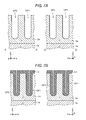
- FIG. 14 is a plan view which shows a semiconductor device according to a second embodiment.
- FIG. 15 is a cross-sectional view of the semiconductor device according to a second embodiment taken along line A-A′ of FIG. 14 .
- FIG. 16 is a cross-sectional view of the semiconductor device according to a second embodiment taken along line B-B′ of FIG. 14 .
- FIG. 17 is a cross-sectional view of the semiconductor device according to a second embodiment taken long line C-C′ of FIG. 14 .
- Embodiments provide a semiconductor device which may suppress a breakdown of a semiconductor device in a reverse recovery state.
- a semiconductor device in general, includes a first semiconductor region of a first conductivity type, a first electrode, a second electrode, a third electrode, a first insulation portion (region), a second insulation portion (region), a second semiconductor region of a second conductivity type, a third semiconductor region of the first conductivity type, a fourth semiconductor region of the second conductivity type, and a fourth electrode.
- the first electrode extends in a first direction.
- the second electrode is provided spaced from the first electrode.
- the second electrode includes a first portion and a second portion. The first portion extends in a second direction intersecting with the first direction. A plurality of first portions are spaced from each other along the first direction. The second portion extends in the first direction.
- the second portion is provided between the plurality of first portions and the first electrode in the second direction.
- the third electrode is provided spaced from the first electrode and the second electrode.
- the first insulation region is provided between the first semiconductor region and the first electrode and between the first semiconductor region and the third electrode.
- the second insulation region is provided between the first semiconductor region and the second electrode.
- the second semiconductor region is provided on the first semiconductor region.
- the second semiconductor region faces the second electrode through the second insulation region.
- the third semiconductor region is selectively provided on the second semiconductor region.
- the fourth semiconductor region is provided on the first semiconductor region.
- the fourth semiconductor region is between adjacent first portions of the second electrode in the first direction.
- the fourth electrode is provided on the third semiconductor region.
- the fourth electrode is electrically connected to the second semiconductor region, the third semiconductor region, the fourth semiconductor region, the first electrode, and the second electrode.
- the drawings are schematic and/or conceptual, such that a relationship between a thickness and a width of each portion, and a size ratio between portions are not necessarily the same as those in an actual device.
- different dimensions or ratios may be depicted in the drawings in some cases.
- the same elements are denoted by the same reference numerals in the specification and in each drawing, and a detailed description of repeated or common element may be omitted.
- An XYZ orthogonal coordinate system is used for a description of each embodiment.
- Two directions which are substantially parallel to a surface of the semiconductor layer S and orthogonal to each other are set to be an X direction (second direction) and a Y direction (first direction), and a direction orthogonal to both of these X and Y directions is set to be a Z direction.
- n + , n ⁇ , p + , p, and p ⁇ shows a relative level of the impurity concentration for each conductivity type. That is, n + shows a relatively higher n-type impurity concentration than n ⁇ . In addition, p + shows a relatively higher p-type impurity concentration than p, and p ⁇ shows a relatively lower p-type impurity concentration than p.
- each embodiment may also be implemented by inverting a p-type and an n-type for each semiconductor region.
- a semiconductor device 100 according to a first embodiment will be described with reference to FIGS. 1 to 6 .
- FIG. 1 is a plan view which shows the semiconductor device 100 according to a first embodiment.
- FIG. 2 is a cross-sectional view taken along line A-A′ of FIG. 1 .
- FIG. 3 is a cross-sectional view taken along line B-B′ of FIG. 1 .
- FIG. 4 is an enlarged plan view of a C portion of FIG. 1 .
- FIG. 5 is an enlarged plan view of a D portion of FIG. 1 .
- FIG. 6 is a cross-sectional view taken along line E-E′ of FIG. 1 .
- first insulation portion 21 Only a first insulation portion 21 , a second insulation portion 22 , and a third insulation portion 23 which are provided in a semiconductor layer S are shown, and the other components are omitted in FIG. 1 for purposes of explanation.
- An insulation layer 24 , a source electrode 31 , a portion of the first insulation portion 21 , and a portion of the second insulation portion 22 are omitted in FIG. 4 for purposes of explanation.
- the insulation layer 24 , the source electrode 31 , a portion of the second insulation portion 22 , and a portion of the third insulation portion 23 are omitted in FIG. 5 for purposes of explanation.
- the semiconductor device 100 according to the first embodiment is, for example, a MOSFET.
- the semiconductor device 100 includes an n + -type drain region 1 , a semiconductor region 2 (first semiconductor region) of an n ⁇ -type (first conductivity type), a base region 3 (second semiconductor region) of a p-type (second conductivity type), an n + -type source region 4 (third semiconductor region), a p + -type contact region 5 (seventh semiconductor region), a p ⁇ -type semiconductor region 6 (fourth semiconductor region), a p + -type semiconductor region 7 (eighth semiconductor region), a p ⁇ -type semiconductor region 8 (fifth semiconductor region), an n + -type semiconductor region 9 (sixth semiconductor region), a gate electrode 11 , a field plate electrode 12 (second electrode), a gate electrode 14 (third electrode), a field plate electrode 15 (first electrode), a gate electrode 16 , a field plate electrode 17 , the first insulation portion 21 , the second insulation portion 22 , the third insulation portion 23 , a drain electrode 30 , and
- the semiconductor device 100 includes the first insulation portion 21 , a plurality of the second insulation portions 22 , and the third insulation portion 23 provided in the semiconductor layer S.
- the first insulation portion 21 , the plurality of second insulation portions 22 , and the third insulation portion 23 are spaced from each other in an X direction.
- the first insulation portion 21 includes a plurality of first insulation portions 21 a and a second insulation portion 21 b.
- the third insulation portion 23 includes a plurality of third insulation portions 23 d and a fourth insulation portion 23 c.
- a plurality of the first insulation portions 21 a and a plurality of the third insulation portions 23 d are provided spaced from each other in a Y direction, each of the first insulation portions 21 a and the third insulation portions 23 d extends in the X direction.
- the second insulation portion 21 b and the fourth insulation portion 23 c extend in the Y direction.
- each of the second insulation portions 22 extends in the Y direction.
- the semiconductor layer S has a front surface S 1 and a rear surface S 2 .
- the source electrode 31 is provided on a side of the front surface S 1 (front surface side) of the semiconductor layer S
- the drain electrode 30 is provided on a side of the rear surface S 2 (back surface side) of the semiconductor layer S.
- the n + -type drain region 1 is provided in the semiconductor layer S on the back surface side at the rear surface S 2 .
- the n + -type drain region 1 is electrically connected to the drain electrode 30 .
- the n ⁇ -type semiconductor region 2 is provided on the n + -type drain region 1 .
- the p-type base region 3 is selectively provided on the n ⁇ -type semiconductor region 2 .
- a plurality of the p-type base regions 3 are provided spaced from each other in the X direction, and each of the p-type base regions 3 extends in the Y direction parallel with the gate electrode 11 .
- each of the p-type base regions 3 is provided between the first insulation portion 21 and a second insulation portion 22 , between adjacent second insulation portions 22 , or between a second insulation portion 22 and the third insulation portion 23 .
- the n + -type source region 4 is selectively provided on the p-type base region 3 .
- a plurality of the n + -type source regions 4 are provided on each of the p-type base regions 3 , and each of the n + -type source regions 4 extends in the Y direction.
- the p + -type contact region 5 is selectively provided on the p-type base region 3 .
- the p + -type contact region 5 is provided between adjacent n + -type source regions 4 on each of the p-type base regions 3 .
- Each of the p + -type contact regions 5 extends in the Y direction.
- the gate electrode 11 and the field plate (FP) electrode 12 are provided spaced from each other in the X direction.
- the gate electrode 11 is provided between the FP electrode 12 and a portion of the n ⁇ -type semiconductor region 2 , the p-type base region 3 , and a portion of the n + -type source regions 4 .
- the first insulation portion 21 is provided between the gate electrode 11 and the FP electrode 12 and the n ⁇ -type semiconductor region 2 , the p-type base region 3 , and the n + -type source regions 4 .
- the FP electrode 12 includes the first electrode portion 12 a and the second electrode portion 12 b .
- a plurality of the first electrode portions 12 a are provided spaced from each other in the Y direction, and each of the first electrode portions 12 a extends in the X direction.
- the second electrode portion 12 b extends in the Y direction.
- the first electrode portion 12 a is in contact with the second electrode portion 12 b.
- the first electrode portion 12 a and the second electrode portion 12 b may be provided spaced from each other in the X direction. That is, a portion of the first insulation portion 21 may be provided between the first electrode portion 12 a and the second electrode portion 12 b.
- the gate electrode 14 and the FP electrode 15 are provided spaced from each other in the X direction.
- the gate electrode 14 and the FP electrode 15 extend in the Y direction, and the FP electrode 15 is provided between adjacent gate electrodes 14 in the X direction.
- the second electrode portion 12 b is positioned between the plurality of first electrode portions 12 a and the gate electrode 14 and the FP electrode 15 in the X direction.
- the second insulation portion 22 is provided between the gate electrode 14 and the FP electrode 15 and between the gate electrode 14 and the n ⁇ -type semiconductor region 2 , the p-type base region 3 , and the n + -type source region 4 .
- the gate electrode 14 faces a portion of the n ⁇ -type semiconductor region 2 , the p-type base region 3 , and a portion of the n + -type source regions 4 through the second insulation portion 22 in the X direction.
- a portion of the FP electrode 15 faces a portion of the n ⁇ -type semiconductor region 2 through the second insulation portion 22 in the X direction—that is, some portion of the FP electrode 15 extends in Z direction beyond the gate electrode 14 .
- the gate electrode 16 and the FP electrode 17 are provided spaced from each other in the X direction.
- the gate electrode 16 is provided between the FP electrode 17 and a portion of the n ⁇ -type semiconductor region 2 , the p-type base region 3 , and a portion of the n + -type source regions 4 in the X direction.
- the third insulation portion 23 is provided between of the gate electrode 16 and the FP electrode 17 and between the gate electrode 16 and each of the n ⁇ -type semiconductor region 2 , the p-type base region 3 , and the n + -type source regions 4 .
- the FP electrode 17 includes a third electrode portion 17 a and a fourth electrode portion 17 b .
- a plurality of the third electrode portions 17 a are provided spaced from each other in the Y direction, and each of the third electrode portions 17 a extends in the X direction.
- the fourth electrode portion 17 b extends in the Y direction.
- the third electrode portion 17 a is in contact with the fourth electrode portion 17 b.
- the gate electrodes 11 , 14 , and 16 are electrically connected to a gate electrode pad which is not specifically depicted.
- the FP electrodes 12 , 15 , and 17 are electrically connected to the source electrode 31 .
- a distance between adjacent first electrode portions 12 a in the Y direction is set as D 1
- a distance between FP electrode 12 and a nearest on of the FP electrodes 15 in the X direction is set as D 2
- a distance between adjacent FP electrodes 15 in the X direction is set as D 3
- a distance between the FP electrode 17 and a nearest one of the FP electrodes 15 in the X direction is set as D 4 .
- each of the FP electrodes ( 12 , 15 , and 17 ) is provided so that the distances D 1 to D 4 are equal to each other.
- a thickness of the first insulation portion 21 between the FP electrode 12 and the n ⁇ -type semiconductor region 2 in the Y direction is set as T 1
- a thickness of the first insulation portion 21 between the FP electrode 12 and the n ⁇ -type semiconductor region 2 in the X direction toward a FP electrode 15 is set as T 2
- a thickness of the second insulation portion 22 between the FP electrode 15 and the n ⁇ -type semiconductor region 2 in the X direction is set as T 3
- a thickness of the third insulation portion 23 between the FP electrode 17 and the n ⁇ -type semiconductor region 2 in the X direction toward a FP electrode 15 is set as T 4 .
- the first insulation portions ( 21 , 22 , and 23 ) and each of the FP electrodes ( 12 , 15 , and 17 ) are provided so that, for example, the thicknesses T 1 to T 4 are equal to each other.
- the p ⁇ -type semiconductor region 6 is selectively provided on the n ⁇ -type semiconductor region 2 . As shown in FIGS. 3 to 5 , the p ⁇ -type semiconductor region 6 is provided between adjacent first electrode portions 12 a in the Y direction and between adjacent third electrode portions 17 a in the Y direction. The second insulation portion 21 b is provided between the p-type base region 3 and the p ⁇ -type semiconductor region 6 in the X direction.
- a portion of the second electrode portion 12 b and a portion of the fourth electrode portion 17 b are provided between the p ⁇ -type semiconductor region 6 and the p-type base region 3 in the X direction.
- the first electrode portion 12 a and the p ⁇ -type semiconductor region 6 , and the third electrode portion 17 a and the p ⁇ -type semiconductor region 6 are provided to intersect with each other in the Y direction.
- a position of at least one portion of the p ⁇ -type semiconductor region 6 in the X direction is equal to a position of at least one portion of the first electrode portion 12 a in the X direction. That is, along the X direction at least a portion of the first electrode portion 12 a overlaps with p ⁇ -type semiconductor region 6 .
- a position of the p ⁇ -type semiconductor region 6 in the Y direction is between positions of two adjacent first electrode portions 12 a in the Y direction.
- a position of at least one portion of the p ⁇ -type semiconductor region 6 in the X direction is equal to a position of at least one portion of the third electrode portion 17 a in the X direction.
- a position of the p ⁇ -type semiconductor region 6 in the Y direction is between positions of two adjacent third electrode portions 17 a in the Y direction.
- the p + -type semiconductor region 7 is selectively provided on the p ⁇ -type semiconductor region 6 .
- a plurality of the p + -type semiconductor regions 7 are provided spaced from each other in the Y direction.
- the p + -type semiconductor regions 7 are electrically connected to the source electrode 31 .
- the p ⁇ -type semiconductor region 8 may be provided on the n ⁇ -type semiconductor region 2 .
- a plurality of the p ⁇ -type semiconductor regions 8 are provided spaced from each other in the X direction.
- the plurality of p ⁇ -type semiconductor regions 8 is similarly provided at each end of the p + -type contact region 5 along the Y direction.
- the n + -type semiconductor region 9 may be further provided on the n ⁇ -type semiconductor region 2 .
- the n + -type semiconductor region 9 is provided on an outer periphery of the semiconductor device 100 so as to surround the p-type base region 3 , the n + -type source region 4 , the p + -type contact region 5 , the p ⁇ -type semiconductor region 6 , the p + -type semiconductor region 7 , and the p ⁇ -type semiconductor region 8 .
- At least one portion of the p-type base region 3 , at least one portion of the n + -type source region 4 , and at least one portion of the p + -type contact region 5 are provided between the p ⁇ -type semiconductor regions 8 in the Y direction as shown in, for example, FIG. 6 .
- a p-type impurity concentration of the p ⁇ -type semiconductor region 6 is equal to a p-type impurity concentration of the p ⁇ -type semiconductor region 8 .
- the p-type impurity concentration of the p ⁇ -type semiconductor region 6 may be equal to the p-type impurity concentration of the p-type base region 3 .
- the source electrode 31 is provided on the front surface S 1 .
- An insulation layer is provided between each gate electrode element and the source electrode 31 , and each gate electrode element is electrically insulated from the source electrode 31 .
- the source electrode 31 is electrically connected to the n + -type source region 4 , the p + -type contact region 5 , and the p + -type semiconductor region 7 .
- the p-type base region 3 is electrically connected to the source electrode through the p + -type contact region 5 .
- the p ⁇ -type semiconductor region 6 is electrically connected to the source electrode 31 through the p + -type semiconductor region 7 .
- the source electrode 31 is electrically connected to the FP electrodes 12 , 15 , and 17 .
- a voltage equal to or greater than a threshold can be applied to the gate electrode, and thereby a channel (inversion layer) will be formed in the p-type base region 3 and a MOSFET is turned on (placed in a conducting state).
- FIGS. 7A to 12B Next, an example of a method of manufacturing the semiconductor device 100 according to a first embodiment will be described referring to FIGS. 7A to 12B .
- FIGS. 7A to 12B are cross-sectional views which show a manufacture process of the semiconductor device 100 according to a first embodiment.
- FIGS. 7A to 12B are sectional views which show a manufacture process at a position corresponding to a F-F′ line of FIG. 4
- drawings on the right side of FIGS. 7A to 12B are cross-sectional views which show a manufacture process at a position corresponding to a G-G′ line of FIG. 4 .
- an n + -type semiconductor substrate (hereinafter, referred to as a substrate) 1 a is prepared. Subsequently, silicon is epitaxially grown while the n-type impurity is doped therein, thereby forming the n ⁇ -type semiconductor layer 2 a on the substrate 1 a .
- the n-type impurity it is possible to use phosphorus or arsenic.
- openings OP 1 and OP 2 are formed in the n ⁇ -type semiconductor layer 2 a .
- a portion of the opening OP 1 extends in the Y direction, and another portion of the opening OP 1 extends in the X direction.
- the opening OP 2 extends in the Y direction.
- the openings OP 1 and OP 2 are formed using a reactive ion etching (RIE) method.
- RIE reactive ion etching
- an insulation layer IL 1 is formed on an inner wall of the opening OP 1 , an inner wall of the opening OP 2 , and an upper surface of the n ⁇ -type semiconductor layer 2 a .
- a material of the insulation layer IL 1 it is possible to use silicon oxide.
- the insulation layer IL 1 is formed using a thermal oxidization method or a chemical vapor deposition (CVD) method.
- the conductive layer contains, for example, poly-silicon, and here is formed by using the CVD method.
- An n-type impurity or a p-type impurity may be doped into the poly-silicon.
- As the p-type impurity it is possible to use boron.
- a portion of the conductive layer is removed by a chemical dry etching (CDE) method.
- CDE chemical dry etching
- the FP electrode 12 is formed in the opening OP 1
- the FP electrode 15 is formed in the opening OP 2 .
- the FP electrode 12 formed in a portion of the opening OP 1 extending in the Y direction is linked to the FP electrode 12 formed in a portion of the opening OP 1 extending in the X direction.
- a portion of the insulation layer IL 1 is selectively removed.
- a side wall of the FP electrode 12 , a side wall of the FP electrode 15 , a portion of the inner wall of the opening OP 1 , and a portion of the inner wall of the opening OP 2 are exposed.
- the portion of the insulation layer IL 1 may be removed, for example, by a wet etching method in which an etching solution including hydrogen fluoride (HF) is used.
- an insulation layer IL 2 is formed by using a thermal oxidization method.
- the insulation layer IL 2 is formed on an exposed portion of the FP electrodes 12 and 15 , an exposed portion of the inner wall of the openings OP 1 and OP 2 , and the upper surface of the n ⁇ -type semiconductor layer 2 a.
- a mask M 1 which covers a portion of the insulation layer IL 2 , is formed.
- the mask M 1 covers a portion of the insulation layer IL 2 that is formed in the opening OP 1 .
- silicon oxide may be used as a material of the mask M 1 .
- a conductive layer is formed.
- the conductive layer is formed of, for example, poly-silicon formed by using a CVD method.
- a portion of this conductive layer formed in the opening OP 1 and other portions of the conductive layer formed outside of the opening OP 2 are removed by, for example, a CDE method.
- the gate electrodes 11 and 14 are formed.
- the insulation layer IL 3 contains, for example, silicon oxide, and is formed by a CVD method. Thereafter, a portion of the insulation layer IL 3 is removed by using a RIE method, and thereby the upper surface of the n ⁇ -type semiconductor layer 2 a is exposed as shown in FIG. 10A .
- each of the first insulation portion 21 , the second insulation portion 22 , and the third insulation portion 23 has a portion of the insulation layer IL 1 , a portion of the insulation layer IL 2 , and a portion of the insulation layer IL 3 .
- a mask M 2 is formed.
- a p-type impurity is ion-implanted into a portion of the n ⁇ -type semiconductor layer 2 a by using the mask M 2 , and thereby the p-type base region 3 and the p ⁇ -type semiconductor region 6 are formed.
- the p-type base region 3 and the p ⁇ -type semiconductor region 6 may be formed by different processes.
- a region other than the p-type base region 3 and the p ⁇ -type semiconductor region 6 corresponds to the n ⁇ -type semiconductor region 2 .
- a mask M 3 which covers a portion of the upper surface of the n ⁇ -type semiconductor layer 2 a , a portion of an upper surface of the p-type base region 3 , and the p ⁇ -type semiconductor region 6 is formed.
- an n-type impurity is ion-implanted into a portion of the p-type base region 3 using the mask M 3 , and thereby the n + -type source region 4 is formed as shown in FIG. 11A .
- a mask M 4 which covers a portion of the upper surface of the n ⁇ -type semiconductor layer 2 a , a portion of the upper surface of the p-type base region 3 , and a portion of the p ⁇ -type semiconductor region 6 is formed.
- a p-type impurity is ion-implanted into a portion of the p-type base region 3 and a portion of the p ⁇ -type semiconductor region 6 using the mask M 4 as shown in FIG. 11B , and thereby the p + -type contact region 5 and the p + -type semiconductor region 7 are formed.
- a conductive layer which is formed on the n + -type source region 4 , the p + -type contact region 5 , p ⁇ -type semiconductor region 6 , and the p + -type semiconductor region 7 .
- the source electrode 31 is formed, as shown in FIG. 12A , by patterning this conductive layer.
- a rear surface (back side) of the substrate 1 a is polished until the substrate 1 a has a predetermined thickness.
- the n + -type drain region 1 can be obtained.
- the drain electrode 30 is formed on the polished rear surface of the substrate, and thereby the semiconductor device 100 is obtained.
- the first embodiment it is possible to reduce a possibility of having a breakdown of a semiconductor device in a reverse recovery state while a decrease in a breakdown voltage of the semiconductor device is also suppressed.
- a semiconductor device according to the comparative example does not include the p ⁇ -type semiconductor region 6 , the p + -type semiconductor region 7 , the first electrode portion 12 a , and the third electrode portion 17 a , unlike the semiconductor device according to the first embodiment.
- a forward current flows between the p + -type contact region 5 and the n + -type drain region 1 .
- the p + -type contact region 5 is selectively formed only in a central portion (element region) of the semiconductor device above the n ⁇ -type semiconductor region 2 .
- the p + -type contact region 5 is selectively formed to be between the first insulation portion 21 and the second insulation portion 22 , between the second insulation portions 22 , and between the second insulation portion 22 and the third insulation portion 23 .
- a current density due to a discharge of holes will be higher than a current density due to a discharge of electrons.
- a p + -type semiconductor region is not provided in an outer periphery portion (terminal region) of the semiconductor device surrounding the element region, and thus, holes are accumulated and the current density is likely to be increased.
- a depletion layer when a semiconductor device includes a FP electrode connected to a source electrode, a depletion layer will expand in the n ⁇ -type semiconductor region which is a drift region due to an electric field generated by the FP electrode.
- the breakdown voltage is improved by the presence of the depletion layer, and as a result, it is possible to increase an n-type impurity concentration in the n ⁇ -type semiconductor region.
- the depletion layer is less likely to expand from the p-type semiconductor region in contact with the n ⁇ -type semiconductor region toward the drift region. Accordingly, when the p-type semiconductor region is provided in an outer periphery portion of the semiconductor device according to the comparative example, with the MOSFET in an off state, the depletion layer will not be sufficiently expanded between the p-type semiconductor region and the n ⁇ -type semiconductor region. For this reason, a device breakdown is more likely to occur at a portion in which the p-type semiconductor region is provided.
- the plurality of first electrode portions 12 a extending in the X direction are provided in a region outside the region in which a plurality of gate electrodes extending in the Y direction are provided.
- the p ⁇ -type semiconductor region 6 and the p + -type semiconductor region 7 are provided between these first electrode portions 12 a .
- the depletion layer may expand in the n ⁇ -type semiconductor region 2 by an electric field generated by the first electrode portion 12 a when the MOSFET is in an off state. Therefore, even when the p ⁇ -type semiconductor region 6 and the p + -type semiconductor region 7 are provided, it is possible to maintain a high breakdown voltage of the semiconductor device.
- a depletion layer expands in the n ⁇ -type semiconductor region 2 by an electric field generated by the third electrode portion 17 a to increase the breakdown voltage of the semiconductor device.
- the p ⁇ -type semiconductor region 6 does not need to be positioned between the entire length of the first electrode portions 12 a along the X direction, and may be positioned between only some portion of the length of the first electrode portions 12 a when viewed from the Z direction. That is, a position of at least one portion of the p ⁇ -type semiconductor region 6 aligns with a position of at least one portion of the first electrode portion 12 a along the Y direction, and a position of the p ⁇ -type semiconductor region 6 in the Y direction may be between positions of two adjacent first electrode portions 12 a in the Y direction.
- a position of at least one portion of the p ⁇ -type semiconductor region 6 aligns with a position of at least one portion of the third electrode portion 17 a in the Y direction, and a position of the p ⁇ -type semiconductor region 6 in the Y direction may be between positions of two adjacent third electrode portions 17 a in the Y direction.
- At least one portion of the FP electrode 12 overlaps in the Y direction with the n ⁇ -type semiconductor region 2 through the first insulation portion 21 .
- at least one portion of the FP electrode 17 overlaps in the Y direction with the n ⁇ -type semiconductor region 2 through the first insulation portion 21 .
- the p + -type contact region 5 is provided on the p-type base region 3 .
- the p + -type semiconductor region 7 is provided on the p ⁇ -type semiconductor region 6 .
- the p ⁇ -type semiconductor regions 8 are provided in at least one of a position between the first insulation portion 21 and the second insulation portion 22 , a position between the second insulation portions 22 , and a position between the second insulation portion 22 and the third insulation portion 23 .
- the p-type base region 3 and the p + -type contact region 5 are provided between the p ⁇ -type semiconductor regions 8 . It is possible to improve a breakdown voltage of a semiconductor device by providing the p ⁇ -type semiconductor regions 8 .
- the n + -type semiconductor region 9 which surrounds the p-type base region 3 , the n + -type source region 4 , and the p ⁇ -type semiconductor region 6 is provided, and thereby it is possible to suppresses a depletion layer from extending from the p-type base region 3 or the p ⁇ -type semiconductor region 6 toward an outer periphery of the semiconductor device 100 .
- a terminal region in the semiconductor device 100 may be decreased in size (e.g., overall die area). Accordingly, it is possible to reduce an amount of accumulation of holes in the terminal region, and to reduce a current density in the reverse recovery state.
- FIG. 13 is a cross-sectional view which shows the semiconductor device 110 according to a modification example of the first embodiment.
- FIG. 13 is a cross-sectional view of the semiconductor device 110 at a position corresponding to an A-A′ cross-section of FIG. 1 .
- the semiconductor device 110 is different from the semiconductor device 100 in that potentials of electrodes surrounded by the second insulation portion 22 differ from the semiconductor device 100 . Elements other than these electrodes ( 14 a / 14 b ) in the semiconductor device 110 are substantially the same as in the semiconductor device 100 .
- the semiconductor device 110 includes an electrode 14 a , an electrode 14 b , and an FP electrode 15 , which are surrounded by the second insulation portion 22 .
- the electrode 14 a and the electrode 14 b may have the same structure as that of the gate electrode(s) 14 in the semiconductor device 100 .
- the electrode 14 a is electrically connected to the source electrode 31 .
- the electrode 14 b is an electrode functioning as a gate electrode and thus is not electrically connected to the source electrode, but rather has a potential which varies with an intended gate potential of the semiconductor device 110 .
- the FP electrode 15 is electrically connected to the source electrode 31 in the same manner as in the semiconductor device 100 .
- a semiconductor device 200 according to a second embodiment will be described with reference to FIGS. 14 to 17 .
- FIG. 14 is a plan view which shows the semiconductor device 200 according to the second embodiment.
- FIG. 15 is an A-A′ cross-sectional view of FIG. 14 .
- FIG. 16 is a B-B′ cross-sectional view of FIG. 14 .
- FIG. 17 is a C-C′ cross-sectional view of FIG. 14 .
- the semiconductor device 200 differs from the semiconductor device 100 in the electrodes respectively surrounded by each of the first insulation portion 21 to the third insulation portion 23 . Other than this difference, the semiconductor device 200 may adopt the same structure as in the semiconductor device 100 .
- the semiconductor device 200 includes the first insulation portion 21 , the second insulation portion 22 , and the third insulation portion 23 in the same manner as the semiconductor device 100 .
- the semiconductor device 200 includes FP electrode 12 and FP electrode 13 , both of which are surrounded by the first insulation portion 21 .
- Gate electrode 14 and FP electrode 15 are both surrounded by the second insulation portion 22 .
- FP electrode 17 and FP electrode 18 are both surrounded by the third insulation portion 23 .
- the FP electrodes 12 , 13 , 17 , and 18 are electrically connected to the source electrode 31 .
- the FP electrode 12 includes the first electrode portion 12 a and the second electrode portion 12 b.
- the FP electrode 13 includes a fifth electrode portion 13 e and a sixth electrode portion 13 f.
- the FP electrode 12 is provided between the FP electrode 13 and the n ⁇ -type semiconductor region 2 in the Z direction.
- a plurality of the first electrode portions 12 a and a plurality of the fifth electrode portions 13 e are provided spaced from each other in the Y direction.
- Each of the first electrode portions 12 a and each of the fifth electrode portions 13 e extend in the X direction.
- the second electrode portion 12 b and the sixth electrode portion 13 f extend along the second insulation portion 21 b in the Y direction.
- the first electrode portion 12 a is in contact with the second electrode portion 12 b
- the fifth electrode portion 13 e is in contact with the sixth electrode portion 13 f.
- the gate electrode 14 faces a portion of the n ⁇ -type semiconductor region 2 , the p-type base region 3 , and at least one portion of the n + -type source region 4 through the second insulation portion 22 in the X direction.
- At least one portion of the FP electrode 15 faces a portion of the n ⁇ -type semiconductor region 2 through the second insulation portion 22 in the X direction.
- at least one portion of the FP electrode 15 overlaps with at least one portion of the gate electrode 14 through the second insulation portion 22 in the Z direction.
- the second electrode portion 12 b is provided between a plurality of first electrode portions 12 a and the FP electrode 15 in the X direction.
- the FP electrode 17 includes the third electrode portion 17 a and the fourth electrode portion 17 b .
- the FP electrode 18 includes a seventh electrode portion 18 b and an eighth electrode portion 18 a .
- the FP electrode 17 is provided between the FP electrode 18 and the n ⁇ -type semiconductor region 2 in the Z direction.
- a plurality of the third electrode portions 17 a are provided spaced from each other in the Y direction.
- a plurality of the seventh electrode portions 18 b are also provided spaced from each in the Y direction.
- Each of the third electrode portions 17 a and each of the seventh electrode portions 18 b extend in the X direction.
- the fourth electrode portion 17 b and the eighth electrode portion 18 a extend along the fourth insulation portion 23 d in the Y direction.
- the third electrode portion 17 a is in contact with the fourth electrode portion 17 b
- the seventh electrode portion 18 b is in contact with the eighth electrode portion 18 a.
- the FP electrode 17 faces a portion of the n ⁇ -type semiconductor region 2 through the third insulation portion 23 in the X direction and the Y direction.
- the FP electrode 18 faces a portion of the n ⁇ -type semiconductor region 2 , the p-type base region 3 , and at least one portion of the n + -type source region 4 through the third insulation portion 23 in the X direction.
- the third insulation portion 23 is provided between the FP electrode 17 and the FP electrode 18 and between the FP electrodes 17 and 18 and each of the n ⁇ -type semiconductor region 2 , the p-type base region 3 , and the n + -type source region 4 .
- only the FP electrode 12 is provided without the FP electrode 13 being provided.
- only the FP electrode 17 may is provided without the FP electrode 18 being provided in the region surrounded by the third insulation portion 23 .
- a position along the X direction of at least one portion of the p ⁇ -type semiconductor region 6 is overlapping with at least one portion of the first electrode portion 12 a along the X direction.
- a position of the p ⁇ -type semiconductor region 6 in the Y direction is between two adjacent first electrode portions 12 a .
- At least one portion of the p ⁇ -type semiconductor region 6 and at least one portion of the p + -type semiconductor region 7 are provided between adjacent fifth electrode portions 13 e.
- a position of at least one portion of the p ⁇ -type semiconductor region 6 in the X direction is equal to a position of at least one portion of the third electrode portion 17 a in the X direction.
- a position of the p ⁇ -type semiconductor region 6 in the Y direction is between positions of two adjacent third electrode portions 17 a in the Y direction.
- At least one portion of the p ⁇ -type semiconductor region 6 and at least one portion of the p + -type semiconductor region 7 are provided between adjacent seventh electrode portions 18 b.
- the second embodiment it is possible to reduce a possibility of having a breakdown of a semiconductor device in a reverse recovery state while a breakdown voltage is maintained in the same manner as in the first embodiment.
- a relative level of impurity concentration between semiconductor regions may be confirmed using, for example, scanning capacitance microscope (SCM).
- SCM scanning capacitance microscope
- a carrier concentration in each semiconductor region may be regarded to be equal to an impurity concentration activated in each semiconductor region. Accordingly, even a relative level of carrier concentration between semiconductor regions may be confirmed using the SCM.
- an impurity concentration in each semiconductor region may be measured by, for example, a secondary ion mass spectrometry (SIMS).
- SIMS secondary ion mass spectrometry
Abstract
A semiconductor device includes a first semiconductor region of a first conductivity type, a first electrode, a second electrode, a third electrode, a first insulation region, a second insulation region, a second semiconductor region of a second conductivity type, a third semiconductor region of the first conductivity type, a fourth semiconductor region of the second conductivity type, and a fourth electrode. The second electrode includes first portions and a second portion. The second portion extends in a first direction. The first portions extend in a direction away from the second portion. The second portion is between the first portions and the first electrode in a second direction. The fourth semiconductor region is positioned between adjacent first electrode portions in the first direction.
Description
This application is based upon and claims the benefit of priority from Japanese Patent Application No. 2015-047417, filed Mar. 10, 2015, the entire contents of which are incorporated herein by reference.
Embodiments described herein relate generally to a semiconductor device.
A semiconductor device such as a metal oxide semiconductor field effect transistor (MOSFET) has a diode embedded therein in some cases. While the MOSFET is in an off state, for example, a current flows in a forward direction of the embedded diode. When a reverse voltage is applied to the diode, electrons accumulated in the diode are discharged to a drain electrode, and holes are discharged to a source electrode. The state in which previously accumulated charge carriers are discharged from the diode is referred to as a reverse recovery state. In the reverse recovery state, a current flows due to the carriers being discharged. When a density of a current flowing is high in the semiconductor device, a breakdown of the semiconductor device may occur in some cases.
Embodiments provide a semiconductor device which may suppress a breakdown of a semiconductor device in a reverse recovery state.
In general, according to one embodiment, a semiconductor device, includes a first semiconductor region of a first conductivity type, a first electrode, a second electrode, a third electrode, a first insulation portion (region), a second insulation portion (region), a second semiconductor region of a second conductivity type, a third semiconductor region of the first conductivity type, a fourth semiconductor region of the second conductivity type, and a fourth electrode. The first electrode extends in a first direction. The second electrode is provided spaced from the first electrode. The second electrode includes a first portion and a second portion. The first portion extends in a second direction intersecting with the first direction. A plurality of first portions are spaced from each other along the first direction. The second portion extends in the first direction. The second portion is provided between the plurality of first portions and the first electrode in the second direction. The third electrode is provided spaced from the first electrode and the second electrode. The first insulation region is provided between the first semiconductor region and the first electrode and between the first semiconductor region and the third electrode. The second insulation region is provided between the first semiconductor region and the second electrode. The second semiconductor region is provided on the first semiconductor region. The second semiconductor region faces the second electrode through the second insulation region. The third semiconductor region is selectively provided on the second semiconductor region. The fourth semiconductor region is provided on the first semiconductor region. The fourth semiconductor region is between adjacent first portions of the second electrode in the first direction. The fourth electrode is provided on the third semiconductor region. The fourth electrode is electrically connected to the second semiconductor region, the third semiconductor region, the fourth semiconductor region, the first electrode, and the second electrode.
Hereinafter, example embodiments will be described by reference to drawings.
The drawings are schematic and/or conceptual, such that a relationship between a thickness and a width of each portion, and a size ratio between portions are not necessarily the same as those in an actual device. In addition, when showing the same portion, different dimensions or ratios may be depicted in the drawings in some cases. The same elements are denoted by the same reference numerals in the specification and in each drawing, and a detailed description of repeated or common element may be omitted.
An XYZ orthogonal coordinate system is used for a description of each embodiment. Two directions which are substantially parallel to a surface of the semiconductor layer S and orthogonal to each other are set to be an X direction (second direction) and a Y direction (first direction), and a direction orthogonal to both of these X and Y directions is set to be a Z direction.
In a following description, a notation of n+, n−, p+, p, and p− shows a relative level of the impurity concentration for each conductivity type. That is, n+ shows a relatively higher n-type impurity concentration than n−. In addition, p+ shows a relatively higher p-type impurity concentration than p, and p− shows a relatively lower p-type impurity concentration than p.
In the embodiments described below, each embodiment may also be implemented by inverting a p-type and an n-type for each semiconductor region.
(First Embodiment)
A semiconductor device 100 according to a first embodiment will be described with reference to FIGS. 1 to 6 .
Only a first insulation portion 21, a second insulation portion 22, and a third insulation portion 23 which are provided in a semiconductor layer S are shown, and the other components are omitted in FIG. 1 for purposes of explanation.
An insulation layer 24, a source electrode 31, a portion of the first insulation portion 21, and a portion of the second insulation portion 22 are omitted in FIG. 4 for purposes of explanation.
The insulation layer 24, the source electrode 31, a portion of the second insulation portion 22, and a portion of the third insulation portion 23 are omitted in FIG. 5 for purposes of explanation.
The semiconductor device 100 according to the first embodiment is, for example, a MOSFET.
The semiconductor device 100 according to the first embodiment includes an n+-type drain region 1, a semiconductor region 2 (first semiconductor region) of an n−-type (first conductivity type), a base region 3 (second semiconductor region) of a p-type (second conductivity type), an n+-type source region 4 (third semiconductor region), a p+-type contact region 5 (seventh semiconductor region), a p−-type semiconductor region 6 (fourth semiconductor region), a p+-type semiconductor region 7 (eighth semiconductor region), a p−-type semiconductor region 8 (fifth semiconductor region), an n+-type semiconductor region 9 (sixth semiconductor region), a gate electrode 11, a field plate electrode 12 (second electrode), a gate electrode 14 (third electrode), a field plate electrode 15 (first electrode), a gate electrode 16, a field plate electrode 17, the first insulation portion 21, the second insulation portion 22, the third insulation portion 23, a drain electrode 30, and a source electrode 31 (fourth electrode).
As shown in FIG. 1 , the semiconductor device 100 includes the first insulation portion 21, a plurality of the second insulation portions 22, and the third insulation portion 23 provided in the semiconductor layer S. The first insulation portion 21, the plurality of second insulation portions 22, and the third insulation portion 23 are spaced from each other in an X direction.
The first insulation portion 21 includes a plurality of first insulation portions 21 a and a second insulation portion 21 b.
The third insulation portion 23 includes a plurality of third insulation portions 23 d and a fourth insulation portion 23 c.
A plurality of the first insulation portions 21 a and a plurality of the third insulation portions 23 d are provided spaced from each other in a Y direction, each of the first insulation portions 21 a and the third insulation portions 23 d extends in the X direction. The second insulation portion 21 b and the fourth insulation portion 23 c extend in the Y direction.
In the X direction, a plurality of the second insulation portions 22 are provided between the first insulation portion 21 and the third insulation portion 23, and each of the second insulation portions 22 extends in the Y direction.
As shown in FIG. 2 , the semiconductor layer S has a front surface S1 and a rear surface S2. The source electrode 31 is provided on a side of the front surface S1 (front surface side) of the semiconductor layer S, and the drain electrode 30 is provided on a side of the rear surface S2 (back surface side) of the semiconductor layer S.
The n+-type drain region 1 is provided in the semiconductor layer S on the back surface side at the rear surface S2. The n+-type drain region 1 is electrically connected to the drain electrode 30. The n−-type semiconductor region 2 is provided on the n+-type drain region 1.
The p-type base region 3 is selectively provided on the n−-type semiconductor region 2. A plurality of the p-type base regions 3 are provided spaced from each other in the X direction, and each of the p-type base regions 3 extends in the Y direction parallel with the gate electrode 11. In addition, each of the p-type base regions 3 is provided between the first insulation portion 21 and a second insulation portion 22, between adjacent second insulation portions 22, or between a second insulation portion 22 and the third insulation portion 23.
As shown in FIGS. 2 and 4 , the n+-type source region 4 is selectively provided on the p-type base region 3. A plurality of the n+-type source regions 4 are provided on each of the p-type base regions 3, and each of the n+-type source regions 4 extends in the Y direction.
As shown in FIGS. 4 and 5 , the p+-type contact region 5 is selectively provided on the p-type base region 3. The p+-type contact region 5 is provided between adjacent n+-type source regions 4 on each of the p-type base regions 3. Each of the p+-type contact regions 5 extends in the Y direction.
The gate electrode 11 and the field plate (FP) electrode 12 are provided spaced from each other in the X direction.
The gate electrode 11 is provided between the FP electrode 12 and a portion of the n−-type semiconductor region 2, the p-type base region 3, and a portion of the n+-type source regions 4. The first insulation portion 21 is provided between the gate electrode 11 and the FP electrode 12 and the n−-type semiconductor region 2, the p-type base region 3, and the n+-type source regions 4.
As shown in FIGS. 2 to 4 , the FP electrode 12 includes the first electrode portion 12 a and the second electrode portion 12 b. A plurality of the first electrode portions 12 a are provided spaced from each other in the Y direction, and each of the first electrode portions 12 a extends in the X direction. The second electrode portion 12 b extends in the Y direction. The first electrode portion 12 a is in contact with the second electrode portion 12 b.
In some embodiments, the first electrode portion 12 a and the second electrode portion 12 b may be provided spaced from each other in the X direction. That is, a portion of the first insulation portion 21 may be provided between the first electrode portion 12 a and the second electrode portion 12 b.
The gate electrode 14 and the FP electrode 15 are provided spaced from each other in the X direction. The gate electrode 14 and the FP electrode 15 extend in the Y direction, and the FP electrode 15 is provided between adjacent gate electrodes 14 in the X direction. The second electrode portion 12 b is positioned between the plurality of first electrode portions 12 a and the gate electrode 14 and the FP electrode 15 in the X direction.
The second insulation portion 22 is provided between the gate electrode 14 and the FP electrode 15 and between the gate electrode 14 and the n−-type semiconductor region 2, the p-type base region 3, and the n+-type source region 4. The gate electrode 14 faces a portion of the n−-type semiconductor region 2, the p-type base region 3, and a portion of the n+-type source regions 4 through the second insulation portion 22 in the X direction. A portion of the FP electrode 15 faces a portion of the n−-type semiconductor region 2 through the second insulation portion 22 in the X direction—that is, some portion of the FP electrode 15 extends in Z direction beyond the gate electrode 14.
The gate electrode 16 and the FP electrode 17 are provided spaced from each other in the X direction.
The gate electrode 16 is provided between the FP electrode 17 and a portion of the n−-type semiconductor region 2, the p-type base region 3, and a portion of the n+-type source regions 4 in the X direction. The third insulation portion 23 is provided between of the gate electrode 16 and the FP electrode 17 and between the gate electrode 16 and each of the n−-type semiconductor region 2, the p-type base region 3, and the n+-type source regions 4.
As shown in FIGS. 2 and 5 , the FP electrode 17 includes a third electrode portion 17 a and a fourth electrode portion 17 b. A plurality of the third electrode portions 17 a are provided spaced from each other in the Y direction, and each of the third electrode portions 17 a extends in the X direction. The fourth electrode portion 17 b extends in the Y direction. The third electrode portion 17 a is in contact with the fourth electrode portion 17 b.
The gate electrodes 11, 14, and 16 are electrically connected to a gate electrode pad which is not specifically depicted. The FP electrodes 12, 15, and 17 are electrically connected to the source electrode 31.
Here, as shown in FIGS. 2 and 3 , a distance between adjacent first electrode portions 12 a in the Y direction is set as D1, a distance between FP electrode 12 and a nearest on of the FP electrodes 15 in the X direction is set as D2, a distance between adjacent FP electrodes 15 in the X direction is set as D3, and a distance between the FP electrode 17 and a nearest one of the FP electrodes 15 in the X direction is set as D4. Here, each of the FP electrodes (12, 15, and 17) is provided so that the distances D1 to D4 are equal to each other.
In addition, as shown in FIGS. 2 and 3 , a thickness of the first insulation portion 21 between the FP electrode 12 and the n−-type semiconductor region 2 in the Y direction is set as T1, a thickness of the first insulation portion 21 between the FP electrode 12 and the n−-type semiconductor region 2 in the X direction toward a FP electrode 15 is set as T2, a thickness of the second insulation portion 22 between the FP electrode 15 and the n−-type semiconductor region 2 in the X direction is set as T3, and a thickness of the third insulation portion 23 between the FP electrode 17 and the n−-type semiconductor region 2 in the X direction toward a FP electrode 15 is set as T4. The first insulation portions (21, 22, and 23) and each of the FP electrodes (12, 15, and 17) are provided so that, for example, the thicknesses T1 to T4 are equal to each other.
The p−-type semiconductor region 6 is selectively provided on the n−-type semiconductor region 2. As shown in FIGS. 3 to 5 , the p−-type semiconductor region 6 is provided between adjacent first electrode portions 12 a in the Y direction and between adjacent third electrode portions 17 a in the Y direction. The second insulation portion 21 b is provided between the p-type base region 3 and the p−-type semiconductor region 6 in the X direction.
As shown in FIGS. 4 and 5 , a portion of the second electrode portion 12 b and a portion of the fourth electrode portion 17 b are provided between the p−-type semiconductor region 6 and the p-type base region 3 in the X direction. In addition, when viewed from a Z direction, the first electrode portion 12 a and the p−-type semiconductor region 6, and the third electrode portion 17 a and the p−-type semiconductor region 6 are provided to intersect with each other in the Y direction.
In other words, with regard to the p−-type semiconductor region 6 provided between adjacent first electrode portions 12 a in the Y direction, a position of at least one portion of the p−-type semiconductor region 6 in the X direction is equal to a position of at least one portion of the first electrode portion 12 a in the X direction. That is, along the X direction at least a portion of the first electrode portion 12 a overlaps with p−-type semiconductor region 6. In addition, a position of the p−-type semiconductor region 6 in the Y direction is between positions of two adjacent first electrode portions 12 a in the Y direction.
In the same manner, with regard to the p−-type semiconductor region 6 provided between adjacent third electrode portions 17 a in the Y direction, a position of at least one portion of the p−-type semiconductor region 6 in the X direction is equal to a position of at least one portion of the third electrode portion 17 a in the X direction. In addition, a position of the p−-type semiconductor region 6 in the Y direction is between positions of two adjacent third electrode portions 17 a in the Y direction.
The p+-type semiconductor region 7 is selectively provided on the p−-type semiconductor region 6. A plurality of the p+-type semiconductor regions 7 are provided spaced from each other in the Y direction. The p+-type semiconductor regions 7 are electrically connected to the source electrode 31.
As shown in FIGS. 4 to 6 , the p−-type semiconductor region 8 may be provided on the n−-type semiconductor region 2. A plurality of the p−-type semiconductor regions 8 are provided spaced from each other in the X direction. The plurality of p−-type semiconductor regions 8 is similarly provided at each end of the p+-type contact region 5 along the Y direction.
As shown in FIGS. 2 to 6 , the n+-type semiconductor region 9 may be further provided on the n−-type semiconductor region 2. The n+-type semiconductor region 9 is provided on an outer periphery of the semiconductor device 100 so as to surround the p-type base region 3, the n+-type source region 4, the p+-type contact region 5, the p−-type semiconductor region 6, the p+-type semiconductor region 7, and the p−-type semiconductor region 8.
At least one portion of the p-type base region 3, at least one portion of the n+-type source region 4, and at least one portion of the p+-type contact region 5 are provided between the p−-type semiconductor regions 8 in the Y direction as shown in, for example, FIG. 6 .
A p-type impurity concentration of the p−-type semiconductor region 6 is equal to a p-type impurity concentration of the p−-type semiconductor region 8. Alternatively, the p-type impurity concentration of the p−-type semiconductor region 6 may be equal to the p-type impurity concentration of the p-type base region 3.
The source electrode 31 is provided on the front surface S1. An insulation layer is provided between each gate electrode element and the source electrode 31, and each gate electrode element is electrically insulated from the source electrode 31. The source electrode 31 is electrically connected to the n+-type source region 4, the p+-type contact region 5, and the p+-type semiconductor region 7. The p-type base region 3 is electrically connected to the source electrode through the p+-type contact region 5. The p−-type semiconductor region 6 is electrically connected to the source electrode 31 through the p+-type semiconductor region 7. In addition, the source electrode 31 is electrically connected to the FP electrodes 12, 15, and 17.
With a positive voltage with respect to the source electrode 31 applied to the drain electrode 30, a voltage equal to or greater than a threshold can be applied to the gate electrode, and thereby a channel (inversion layer) will be formed in the p-type base region 3 and a MOSFET is turned on (placed in a conducting state).
Next, an example of a method of manufacturing the semiconductor device 100 according to a first embodiment will be described referring to FIGS. 7A to 12B .
Drawings on the left side in FIGS. 7A to 12B are sectional views which show a manufacture process at a position corresponding to a F-F′ line of FIG. 4 , and drawings on the right side of FIGS. 7A to 12B are cross-sectional views which show a manufacture process at a position corresponding to a G-G′ line of FIG. 4 .
Here, an n+-type semiconductor substrate (hereinafter, referred to as a substrate) 1 a is prepared. Subsequently, silicon is epitaxially grown while the n-type impurity is doped therein, thereby forming the n−-type semiconductor layer 2 a on the substrate 1 a. As the n-type impurity, it is possible to use phosphorus or arsenic.
Then, as shown in FIG. 7A , openings OP1 and OP2 are formed in the n−-type semiconductor layer 2 a. A portion of the opening OP1 extends in the Y direction, and another portion of the opening OP1 extends in the X direction. The opening OP2 extends in the Y direction. Here, the openings OP1 and OP2 are formed using a reactive ion etching (RIE) method.
Then, as shown in FIG. 7B , an insulation layer IL1 is formed on an inner wall of the opening OP1, an inner wall of the opening OP2, and an upper surface of the n−-type semiconductor layer 2 a. As a material of the insulation layer IL1, it is possible to use silicon oxide. Here, the insulation layer IL1 is formed using a thermal oxidization method or a chemical vapor deposition (CVD) method.
Then, a conductive layer is formed to fill the remaining portions of the openings OP1 and OP2. The conductive layer contains, for example, poly-silicon, and here is formed by using the CVD method. An n-type impurity or a p-type impurity may be doped into the poly-silicon. As the p-type impurity, it is possible to use boron.
Then, as shown in FIG. 8A , a portion of the conductive layer is removed by a chemical dry etching (CDE) method. The conductive layer is etched until a position of an upper end of the conductive layer is equal to a position of an upper end of the n−-type semiconductor layer 2 a, for example.
By this process, the FP electrode 12 is formed in the opening OP1, and the FP electrode 15 is formed in the opening OP2. The FP electrode 12 formed in a portion of the opening OP1 extending in the Y direction is linked to the FP electrode 12 formed in a portion of the opening OP1 extending in the X direction.
Next, as shown in FIG. 8B , a portion of the insulation layer IL1 is selectively removed. By this process, a side wall of the FP electrode 12, a side wall of the FP electrode 15, a portion of the inner wall of the opening OP1, and a portion of the inner wall of the opening OP2 are exposed. The portion of the insulation layer IL1 may be removed, for example, by a wet etching method in which an etching solution including hydrogen fluoride (HF) is used.
Then, as shown in FIG. 9A , an insulation layer IL2 is formed by using a thermal oxidization method. The insulation layer IL2 is formed on an exposed portion of the FP electrodes 12 and 15, an exposed portion of the inner wall of the openings OP1 and OP2, and the upper surface of the n−-type semiconductor layer 2 a.
Then, a mask M1, which covers a portion of the insulation layer IL2, is formed. The mask M1 covers a portion of the insulation layer IL2 that is formed in the opening OP1. As a material of the mask M1, silicon oxide may be used.
Then, a conductive layer is formed. The conductive layer is formed of, for example, poly-silicon formed by using a CVD method. Subsequently, as shown in FIG. 9B , a portion of this conductive layer formed in the opening OP1 and other portions of the conductive layer formed outside of the opening OP2 are removed by, for example, a CDE method. By this process, the gate electrodes 11 and 14 are formed.
Then, an insulation layer IL3 is formed so as to cover the insulation layer IL2 and each gate electrode (11 and 14). The insulation layer IL3 contains, for example, silicon oxide, and is formed by a CVD method. Thereafter, a portion of the insulation layer IL3 is removed by using a RIE method, and thereby the upper surface of the n−-type semiconductor layer 2 a is exposed as shown in FIG. 10A .
By this process, the first insulation portion 21, the second insulation portion 22, and the third insulation portion 23 are formed. That is, each of the first insulation portion 21, the second insulation portion 22, and the third insulation portion 23 has a portion of the insulation layer IL1, a portion of the insulation layer IL2, and a portion of the insulation layer IL3.
Then, a mask M2 is formed. Subsequently, as shown in FIG. 10B , a p-type impurity is ion-implanted into a portion of the n−-type semiconductor layer 2 a by using the mask M2, and thereby the p-type base region 3 and the p−-type semiconductor region 6 are formed. In some embodiments, the p-type base region 3 and the p−-type semiconductor region 6 may be formed by different processes. In the n−-type semiconductor layer 2 a, a region other than the p-type base region 3 and the p−-type semiconductor region 6 corresponds to the n−-type semiconductor region 2.
Then, a mask M3 which covers a portion of the upper surface of the n−-type semiconductor layer 2 a, a portion of an upper surface of the p-type base region 3, and the p−-type semiconductor region 6 is formed. Subsequently, an n-type impurity is ion-implanted into a portion of the p-type base region 3 using the mask M3, and thereby the n+-type source region 4 is formed as shown in FIG. 11A .
Then, a mask M4 which covers a portion of the upper surface of the n−-type semiconductor layer 2 a, a portion of the upper surface of the p-type base region 3, and a portion of the p−-type semiconductor region 6 is formed. Subsequently, a p-type impurity is ion-implanted into a portion of the p-type base region 3 and a portion of the p−-type semiconductor region 6 using the mask M4 as shown in FIG. 11B , and thereby the p+-type contact region 5 and the p+-type semiconductor region 7 are formed.
Then, a conductive layer which is formed on the n+-type source region 4, the p+-type contact region 5, p−-type semiconductor region 6, and the p+-type semiconductor region 7. The source electrode 31 is formed, as shown in FIG. 12A , by patterning this conductive layer.
Then, a rear surface (back side) of the substrate 1 a is polished until the substrate 1 a has a predetermined thickness. By this process, the n+-type drain region 1 can be obtained. Subsequently, as shown in FIG. 12B , the drain electrode 30 is formed on the polished rear surface of the substrate, and thereby the semiconductor device 100 is obtained.
Here, an operation and an effect of the first embodiment will be described.
According to the first embodiment, it is possible to reduce a possibility of having a breakdown of a semiconductor device in a reverse recovery state while a decrease in a breakdown voltage of the semiconductor device is also suppressed.
A reason for this will be described referring to a comparative example described below. A semiconductor device according to the comparative example does not include the p−-type semiconductor region 6, the p+-type semiconductor region 7, the first electrode portion 12 a, and the third electrode portion 17 a, unlike the semiconductor device according to the first embodiment.
When a MOSFET is in an off state (non-conducting state) and a positive voltage with respect to the source electrode 31 is applied to the drain electrode 30, with the source electrode 31 serving as an anode electrode, and the drain electrode 30 serving as a cathode electrode, a forward current flows between the p+-type contact region 5 and the n+-type drain region 1.
Then, when a positive voltage with respect to the source electrode 31 is applied to the drain electrode 30, carriers accumulated in the n−-type semiconductor region 2 are discharged through any one of the drain electrode 30 and the source electrode 31. Specifically, an electron is discharged through the drain electrode 30, and a hole is discharged through the source electrode 31.
At this time, in a case of the semiconductor device according to the comparative example, while the n+-type drain region 1 and the drain electrode 30 are formed over the entire surface under the n−-type semiconductor region 2, the p+-type contact region 5 is selectively formed only in a central portion (element region) of the semiconductor device above the n−-type semiconductor region 2. Specifically, in a case of the semiconductor device according to a comparative example, the p+-type contact region 5 is selectively formed to be between the first insulation portion 21 and the second insulation portion 22, between the second insulation portions 22, and between the second insulation portion 22 and the third insulation portion 23.
Therefore, a current density due to a discharge of holes will be higher than a current density due to a discharge of electrons. In particular, a p+-type semiconductor region is not provided in an outer periphery portion (terminal region) of the semiconductor device surrounding the element region, and thus, holes are accumulated and the current density is likely to be increased.
In this regard, it may be considered to provide a p-type semiconductor region in the terminal region and thus to promote a discharge of the holes. However, adopting this arrangement will generally cause a breakdown voltage of the semiconductor device to be lowered when an FP electrode is provided in the semiconductor device.
Specifically, when a semiconductor device includes a FP electrode connected to a source electrode, a depletion layer will expand in the n−-type semiconductor region which is a drift region due to an electric field generated by the FP electrode. The breakdown voltage is improved by the presence of the depletion layer, and as a result, it is possible to increase an n-type impurity concentration in the n−-type semiconductor region.
By increasing the n-type impurity concentration in the n−-type semiconductor region, on-resistance may be reduced; however, the depletion layer is less likely to expand from the p-type semiconductor region in contact with the n−-type semiconductor region toward the drift region. Accordingly, when the p-type semiconductor region is provided in an outer periphery portion of the semiconductor device according to the comparative example, with the MOSFET in an off state, the depletion layer will not be sufficiently expanded between the p-type semiconductor region and the n−-type semiconductor region. For this reason, a device breakdown is more likely to occur at a portion in which the p-type semiconductor region is provided.
In contrast, in the first embodiment, the plurality of first electrode portions 12 a extending in the X direction are provided in a region outside the region in which a plurality of gate electrodes extending in the Y direction are provided. Also, the p−-type semiconductor region 6 and the p+-type semiconductor region 7 are provided between these first electrode portions 12 a. By adopting such a configuration the depletion layer may expand in the n−-type semiconductor region 2 by an electric field generated by the first electrode portion 12 a when the MOSFET is in an off state. Therefore, even when the p−-type semiconductor region 6 and the p+-type semiconductor region 7 are provided, it is possible to maintain a high breakdown voltage of the semiconductor device.
In the same manner, with respect to the third electrode portion 17 a, a depletion layer expands in the n−-type semiconductor region 2 by an electric field generated by the third electrode portion 17 a to increase the breakdown voltage of the semiconductor device.
In addition, since a hole is efficiently discharged to the source electrode 31 through the p−-type semiconductor region 6 in the reverse recovery state, a current density is kept low. As a result, according to the first embodiment, it is possible to reduce a possibility of having a breakdown of a semiconductor device in a reverse recovery state while maintaining a breakdown voltage of the semiconductor device.
The p−-type semiconductor region 6 does not need to be positioned between the entire length of the first electrode portions 12 a along the X direction, and may be positioned between only some portion of the length of the first electrode portions 12 a when viewed from the Z direction. That is, a position of at least one portion of the p−-type semiconductor region 6 aligns with a position of at least one portion of the first electrode portion 12 a along the Y direction, and a position of the p−-type semiconductor region 6 in the Y direction may be between positions of two adjacent first electrode portions 12 a in the Y direction.
In the same manner, with respect to a relationship between the p−-type semiconductor region 6 and the third electrode portion 17 a, a position of at least one portion of the p−-type semiconductor region 6 aligns with a position of at least one portion of the third electrode portion 17 a in the Y direction, and a position of the p−-type semiconductor region 6 in the Y direction may be between positions of two adjacent third electrode portions 17 a in the Y direction.
In addition, at least one portion of the FP electrode 12 overlaps in the Y direction with the n−-type semiconductor region 2 through the first insulation portion 21. Similarly, at least one portion of the FP electrode 17 overlaps in the Y direction with the n−-type semiconductor region 2 through the first insulation portion 21. Thereby, a depletion layer is likely to expand in a region between the FP electrode 12 and the n−-type semiconductor region 2. Therefore, it is possible to further reduce a possibility of having a breakdown of a semiconductor device in a region in which the p−-type semiconductor region 6 is provided.
The p+-type contact region 5 is provided on the p-type base region 3. The p+-type semiconductor region 7 is provided on the p−-type semiconductor region 6. Thereby, a discharge of holes in a reverse recovery state is efficiently performed and the current density is not increased.
The p−-type semiconductor regions 8 are provided in at least one of a position between the first insulation portion 21 and the second insulation portion 22, a position between the second insulation portions 22, and a position between the second insulation portion 22 and the third insulation portion 23. The p-type base region 3 and the p+-type contact region 5 are provided between the p−-type semiconductor regions 8. It is possible to improve a breakdown voltage of a semiconductor device by providing the p−-type semiconductor regions 8.
Moreover, the n+-type semiconductor region 9 which surrounds the p-type base region 3, the n+-type source region 4, and the p−-type semiconductor region 6 is provided, and thereby it is possible to suppresses a depletion layer from extending from the p-type base region 3 or the p−-type semiconductor region 6 toward an outer periphery of the semiconductor device 100. When the depletion layer is suppressed in this manner, a terminal region in the semiconductor device 100 may be decreased in size (e.g., overall die area). Accordingly, it is possible to reduce an amount of accumulation of holes in the terminal region, and to reduce a current density in the reverse recovery state.
Modification Example of First Embodiment
A plan view of the semiconductor device 110 according to the modification example is the same as the plan view shown in FIG. 1 . FIG. 13 is a cross-sectional view of the semiconductor device 110 at a position corresponding to an A-A′ cross-section of FIG. 1 .
The semiconductor device 110 is different from the semiconductor device 100 in that potentials of electrodes surrounded by the second insulation portion 22 differ from the semiconductor device 100. Elements other than these electrodes (14 a/14 b) in the semiconductor device 110 are substantially the same as in the semiconductor device 100.
As shown in FIG. 13 , the semiconductor device 110 includes an electrode 14 a, an electrode 14 b, and an FP electrode 15, which are surrounded by the second insulation portion 22. The electrode 14 a and the electrode 14 b may have the same structure as that of the gate electrode(s) 14 in the semiconductor device 100. Here, the electrode 14 a is electrically connected to the source electrode 31. The electrode 14 b is an electrode functioning as a gate electrode and thus is not electrically connected to the source electrode, but rather has a potential which varies with an intended gate potential of the semiconductor device 110. The FP electrode 15 is electrically connected to the source electrode 31 in the same manner as in the semiconductor device 100.
Even with this modification, it is possible to reduce a possibility of having a breakdown of a semiconductor device in a reverse recovery state while a breakdown voltage is suppressed not to be lowered in the same manner as in the semiconductor device 100.
In addition, it is possible to decrease the total number of gate electrodes in the semiconductor device 110 according to this modification example, as compared to the semiconductor device 100. Therefore, compared to the semiconductor device 100, it is possible to reduce an overall gate capacitance value and thus to improve a switching speed.
(Second Embodiment)
A semiconductor device 200 according to a second embodiment will be described with reference to FIGS. 14 to 17 .
Only the first insulation portion 21, the second insulation portion 22, and the third insulation portion 23 provided in the semiconductor layer S are shown in FIG. 14 , and the other components are omitted for purposes of explanation.
The semiconductor device 200 differs from the semiconductor device 100 in the electrodes respectively surrounded by each of the first insulation portion 21 to the third insulation portion 23. Other than this difference, the semiconductor device 200 may adopt the same structure as in the semiconductor device 100.
As shown in FIG. 14 , the semiconductor device 200 includes the first insulation portion 21, the second insulation portion 22, and the third insulation portion 23 in the same manner as the semiconductor device 100.
As shown in FIG. 15 , the semiconductor device 200 includes FP electrode 12 and FP electrode 13, both of which are surrounded by the first insulation portion 21. Gate electrode 14 and FP electrode 15 are both surrounded by the second insulation portion 22. FP electrode 17 and FP electrode 18 are both surrounded by the third insulation portion 23. Here, the FP electrodes 12, 13, 17, and 18 are electrically connected to the source electrode 31.
The FP electrode 12 includes the first electrode portion 12 a and the second electrode portion 12 b.
The FP electrode 13 includes a fifth electrode portion 13 e and a sixth electrode portion 13 f.
The FP electrode 12 is provided between the FP electrode 13 and the n−-type semiconductor region 2 in the Z direction. A plurality of the first electrode portions 12 a and a plurality of the fifth electrode portions 13 e are provided spaced from each other in the Y direction. Each of the first electrode portions 12 a and each of the fifth electrode portions 13 e extend in the X direction. The second electrode portion 12 b and the sixth electrode portion 13 f extend along the second insulation portion 21 b in the Y direction. The first electrode portion 12 a is in contact with the second electrode portion 12 b, and the fifth electrode portion 13 e is in contact with the sixth electrode portion 13 f.
The gate electrode 14 faces a portion of the n−-type semiconductor region 2, the p-type base region 3, and at least one portion of the n+-type source region 4 through the second insulation portion 22 in the X direction. At least one portion of the FP electrode 15 faces a portion of the n−-type semiconductor region 2 through the second insulation portion 22 in the X direction. In addition, at least one portion of the FP electrode 15 overlaps with at least one portion of the gate electrode 14 through the second insulation portion 22 in the Z direction. The second electrode portion 12 b is provided between a plurality of first electrode portions 12 a and the FP electrode 15 in the X direction.
As depicted in FIG. 15 , the FP electrode 17 includes the third electrode portion 17 a and the fourth electrode portion 17 b. The FP electrode 18 includes a seventh electrode portion 18 b and an eighth electrode portion 18 a. The FP electrode 17 is provided between the FP electrode 18 and the n−-type semiconductor region 2 in the Z direction. A plurality of the third electrode portions 17 a are provided spaced from each other in the Y direction. A plurality of the seventh electrode portions 18 b are also provided spaced from each in the Y direction. Each of the third electrode portions 17 a and each of the seventh electrode portions 18 b extend in the X direction. The fourth electrode portion 17 b and the eighth electrode portion 18 a extend along the fourth insulation portion 23 d in the Y direction. The third electrode portion 17 a is in contact with the fourth electrode portion 17 b, and the seventh electrode portion 18 b is in contact with the eighth electrode portion 18 a.
The FP electrode 17 faces a portion of the n−-type semiconductor region 2 through the third insulation portion 23 in the X direction and the Y direction. The FP electrode 18 faces a portion of the n−-type semiconductor region 2, the p-type base region 3, and at least one portion of the n+-type source region 4 through the third insulation portion 23 in the X direction. The third insulation portion 23 is provided between the FP electrode 17 and the FP electrode 18 and between the FP electrodes 17 and 18 and each of the n−-type semiconductor region 2, the p-type base region 3, and the n+-type source region 4.
In some embodiments, in the region surrounded by the first insulation portion 21, only the FP electrode 12 is provided without the FP electrode 13 being provided. In the same manner, in some embodiments only the FP electrode 17 may is provided without the FP electrode 18 being provided in the region surrounded by the third insulation portion 23.
As shown in FIG. 16 , a position along the X direction of at least one portion of the p−-type semiconductor region 6 is overlapping with at least one portion of the first electrode portion 12 a along the X direction. A position of the p−-type semiconductor region 6 in the Y direction is between two adjacent first electrode portions 12 a. At least one portion of the p−-type semiconductor region 6 and at least one portion of the p+-type semiconductor region 7 are provided between adjacent fifth electrode portions 13 e.
As shown in FIG. 17 , a position of at least one portion of the p−-type semiconductor region 6 in the X direction is equal to a position of at least one portion of the third electrode portion 17 a in the X direction. A position of the p−-type semiconductor region 6 in the Y direction is between positions of two adjacent third electrode portions 17 a in the Y direction. At least one portion of the p−-type semiconductor region 6 and at least one portion of the p+-type semiconductor region 7 are provided between adjacent seventh electrode portions 18 b.
In the second embodiment, it is possible to reduce a possibility of having a breakdown of a semiconductor device in a reverse recovery state while a breakdown voltage is maintained in the same manner as in the first embodiment.
In each example embodiment described above, a relative level of impurity concentration between semiconductor regions may be confirmed using, for example, scanning capacitance microscope (SCM). A carrier concentration in each semiconductor region may be regarded to be equal to an impurity concentration activated in each semiconductor region. Accordingly, even a relative level of carrier concentration between semiconductor regions may be confirmed using the SCM.
In addition, an impurity concentration in each semiconductor region may be measured by, for example, a secondary ion mass spectrometry (SIMS).
However, the above embodiments are only presented as examples and are not intended to limit a scope of the present disclosure. The aspects of these embodiments described herein may be embodied in other various forms, and various omission, substitutions, changes, and the like may be performed without departing from the scope of the present disclosure. With respect to a specific configuration of each element such as n+-type drain region, an n−-type semiconductor region, a p-type base region, an n+-type source region, a p+-type contact region, a gate electrode, a drain electrode, and a source electrode, which are included in an embodiment, those skilled in the art may appropriately select from known technologies. These embodiments and the modification example fall within the scope and spirit of the present disclosure, and are included in a scope of the present disclosure and its equivalents as set forth in the appended claims. Moreover, each embodiment described above may be implemented in combination with one another.
While certain embodiments have been described, these embodiments have been presented by way of example only, and are not intended to limit the scope of the inventions. Indeed, the novel embodiments described herein may be embodied in a variety of other forms; furthermore, various omissions, substitutions and changes in the form of the embodiments described herein may be made without departing from the spirit of the inventions. The accompanying claims and their equivalents are intended to cover such forms or modifications as would fall within the scope and spirit of the inventions.
Claims (19)
1. A semiconductor device, comprising:
a first semiconductor region of a first conductivity type;
a first electrode extending in a first direction;
a second electrode spaced from the first electrode and including:
a plurality of first portions spaced from each other along the first direction, each first portion extending in a second direction intersecting the first direction, and
a second portion extending in the first direction between the plurality of first portions, the second portion being between the plurality of first portions and the first electrode in the second direction;
a third electrode spaced from the first electrode and the second electrode in the second direction;
a first insulation region between the first semiconductor region and the second electrode;
a second insulation region between the first semiconductor region and the first electrode and between the first semiconductor region and the third electrode;
a second semiconductor region of a second conductivity type on the first semiconductor region and adjacent to the third electrode through the second insulation region;
a third semiconductor region of the first conductivity type on the second semiconductor region;
a fourth semiconductor region of the second conductivity type on the first semiconductor region and between, in the first direction, adjacent first portions of the second electrode; and
a fourth electrode on the third semiconductor region and electrically connected to the second semiconductor region, the third semiconductor region, the fourth semiconductor region, the first electrode, and the second electrode.
2. The semiconductor device according to claim 1 , wherein the first insulation region includes:
a plurality of first portions spaced from each other along the first direction, each first portion extending in the second direction, and
a second portion extending in the first direction and between the second insulation region and the plurality of first portions of the first insulation region in the second direction,
the first portions of the second electrode being in the plurality of first portions of the first insulation region, and
the second portion of the second electrode is in the second portion of the first insulation region.
3. The semiconductor device according to claim 2 , wherein the fourth semiconductor region is between adjacent first portions of the first insulating region in the first direction.
4. The semiconductor device according to claim 1 , further comprising:
a plurality of fifth semiconductor regions of the second conductivity type on the first semiconductor region, wherein
a carrier concentration in the plurality of fifth semiconductor regions is lower than a carrier concentration in the second semiconductor region, and
the second semiconductor region is between adjacent fifth semiconductor regions in the first direction.
5. The semiconductor device according to claim 4 , wherein a carrier concentration in the fourth semiconductor region is equal to a carrier concentration in the plurality of fifth semiconductor regions.
6. The semiconductor device according to claim 1 , further comprising:
a sixth semiconductor region of the first conductivity type on the first semiconductor region and surrounding the second semiconductor region, the third semiconductor region, and the fourth semiconductor region in a plane parallel to the first and second directions, wherein
a carrier concentration in the sixth semiconductor region is higher than a carrier concentration in the first semiconductor region.
7. The semiconductor device according to claim 1 , wherein a distance between adjacent first portions of the second electrode in the first direction is equal to a distance between the first electrode and the second electrode in the second direction.
8. The semiconductor device according to claim 1 , further comprising:
a seventh semiconductor region of the second conductivity type on the second semiconductor region, and
an eighth semiconductor region of the second conductivity type on the fourth semiconductor region, wherein
a carrier concentration in the seventh semiconductor region is higher than a carrier concentration in the second semiconductor region, and
a carrier concentration in the eighth semiconductor region is higher than a carrier concentration in the fourth semiconductor region.
9. The semiconductor device according to claim 8 , further comprising:
a fifth electrode spaced from the second electrode and between the second semiconductor region and the second electrode in the second direction, wherein
a portion of the first insulation region is between the second semiconductor region and the fifth electrode.
10. The semiconductor device according to claim 1 , further comprising:
a sixth electrode spaced from the first and second electrode and electrically connected to the fourth electrode, the sixth electrode including:
a plurality of third portions spaced from each other along the first direction, each third portion extending in the second direction, and
a fourth portion extending in the first direction between the plurality of third portions, the fourth portion being between the plurality of third portion and the first electrode in the second direction; and
a third insulation region between the first semiconductor region and the sixth electrode, wherein
the second insulation region is between the first insulation region and the third insulation region in the second direction.
11. The semiconductor device according to claim 10 , wherein
a plurality of second insulation regions, a plurality of first electrodes, a plurality of third electrodes, a plurality of second semiconductor regions, and a plurality of third semiconductor regions are between the second and sixth electrodes in the second direction,
each of the plurality of first electrodes and each of the plurality of third electrodes being in one of the plurality of the second insulation regions, and
the plurality of second insulation regions are between the first insulation region and the third insulation region.
12. A semiconductor device, comprising:
a first semiconductor region of a first conductivity type;
a first electrode extending in a first direction;
a second electrode spaced from the first electrode and including:
a plurality of first portions spaced from each other along the first direction and extending in a second direction intersecting the first direction, and
a second portion extending in the first direction between the plurality of first portions, the second portion being between the plurality of first portions and the first electrode in the second direction;
a third electrode spaced from the first electrode and the second electrode;
a first insulation region between the first semiconductor region and the second electrode;
a second insulation region between the first semiconductor region and the first electrode and between the first semiconductor region and the third electrode;
a second semiconductor region of a second conductivity type on the first semiconductor region and adjacent to the third electrode via the second insulation region;
a third semiconductor region of the first conductivity type on the second semiconductor region;
a fourth semiconductor region of the second conductivity type on the first semiconductor region, the first insulation region being between the fourth semiconductor region and the second semiconductor region in the second direction, and between adjacent first portions of the second electrode in the first direction; and
a fourth electrode on the third semiconductor region and electrically connected to the second semiconductor region, the third semiconductor region, the fourth semiconductor region, the first electrode, and the second electrode.
13. The semiconductor device according to claim 12 , further comprising:
a fifth semiconductor region of the second conductivity type on the second semiconductor region, and
an sixth semiconductor region of the second conductivity type on the fourth semiconductor region, wherein
a carrier concentration in the fifth semiconductor region is higher than a carrier concentration in the second semiconductor region, and
a carrier concentration in the sixth semiconductor region is higher than a carrier concentration in the fourth semiconductor region.
14. The semiconductor device according to claim 12 , further comprising:
a fifth electrode on the first semiconductor region, the first semiconductor region being between the fourth electrode and the fifth electrode; and
a sixth electrode between the third electrode and the fifth electrode.
15. The semiconductor device according to claim 12 , wherein the semiconductor device is a vertical gate metal-oxide-semiconductor field-effect transistor device.
16. A semiconductor device, comprising:
a first semiconductor region of a first conductivity type;
a first electrode extending in a first direction;
a second electrode spaced from the first electrode and including:
a plurality of first portions spaced from each other along the first direction, each first portion extending in a second direction intersecting the first direction, and
a second portion extending in the first direction between the plurality of first portions, the second portion being between the plurality of first portions and the first electrode in the second direction;
a first insulation region between the first semiconductor region and the second electrode;
a second insulation region between the first semiconductor region and the first electrode;
a second semiconductor region of a second conductivity type on the first semiconductor region and adjacent to the first electrode through the second insulation region;
a third semiconductor region of the first conductivity type on the second semiconductor region; and
a third electrode on the third semiconductor region and electrically connected to the second semiconductor region, the third semiconductor region, and the second electrode.
17. The semiconductor device according to claim 16 , further comprising:
a fourth semiconductor region of the second conductivity type on the first semiconductor region, the fourth semiconductor region being electrically connected to the third electrode and between adjacent pairs of first portions in the first direction.
18. The semiconductor device according to 16, wherein the plurality of first portions directly contact the second portion.
19. The semiconductor device according to 16, wherein a width of each first portion in the first direction is less than a width of each first portion in the second direction.
Applications Claiming Priority (2)
| Application Number | Priority Date | Filing Date | Title |
|---|---|---|---|
| JP2015-047417 | 2015-03-10 | ||
| JP2015047417A JP6334438B2 (en) | 2015-03-10 | 2015-03-10 | Semiconductor device |
Publications (2)
| Publication Number | Publication Date |
|---|---|
| US20160268419A1 US20160268419A1 (en) | 2016-09-15 |
| US9614072B2 true US9614072B2 (en) | 2017-04-04 |
Family
ID=56888214
Family Applications (1)
| Application Number | Title | Priority Date | Filing Date |
|---|---|---|---|
| US14/819,049 Active US9614072B2 (en) | 2015-03-10 | 2015-08-05 | Semiconductor device |
Country Status (3)
| Country | Link |
|---|---|
| US (1) | US9614072B2 (en) |
| JP (1) | JP6334438B2 (en) |
| CN (1) | CN105977295B (en) |
Families Citing this family (3)
| Publication number | Priority date | Publication date | Assignee | Title |
|---|---|---|---|---|
| JP6649216B2 (en) | 2016-09-16 | 2020-02-19 | 株式会社東芝 | Semiconductor device and manufacturing method thereof |
| JP6926012B2 (en) * | 2018-02-14 | 2021-08-25 | 株式会社東芝 | Semiconductor device |
| JP7224979B2 (en) * | 2019-03-15 | 2023-02-20 | 株式会社東芝 | semiconductor equipment |
Citations (7)
| Publication number | Priority date | Publication date | Assignee | Title |
|---|---|---|---|---|
| US6833583B2 (en) | 2001-09-13 | 2004-12-21 | Koninklijke Philips Electronics N.V. | Edge termination in a trench-gate MOSFET |
| US20050167749A1 (en) * | 2001-09-07 | 2005-08-04 | Power Integrations, Inc. | High-voltage vertical transistor with edge termination structure |
| US20110169103A1 (en) * | 2010-01-12 | 2011-07-14 | Maxpower Semiconductor Inc. | Devices, components and methods combining trench field plates with immobile electrostatic charge |
| US20130062688A1 (en) * | 2011-09-13 | 2013-03-14 | Kabushiki Kaisha Toshiba | Semiconductor device and method for manufacturing same |
| US20130248994A1 (en) | 2012-03-23 | 2013-09-26 | Kabushiki Kaisha Toshiba | Power semiconductor device |
| US20140084333A1 (en) | 2012-09-24 | 2014-03-27 | Kabushiki Kaisha Toshiba | Power semiconductor device |
| US8889511B2 (en) * | 2003-05-20 | 2014-11-18 | Fairchild Semiconductor Corporation | Methods of manufacturing power semiconductor devices with trenched shielded split gate transistor |
Family Cites Families (8)
| Publication number | Priority date | Publication date | Assignee | Title |
|---|---|---|---|---|
| US6693011B2 (en) * | 2001-10-02 | 2004-02-17 | Fraunhofer-Gesellschaft Zur Foerderung Der Angewandten Forschung E.V. | Power MOS element and method for producing the same |
| DE102004052678B3 (en) * | 2004-10-29 | 2006-06-14 | Infineon Technologies Ag | Power trench transistor |
| WO2006082617A1 (en) * | 2005-01-31 | 2006-08-10 | Shindengen Electric Manufacturing Co., Ltd. | Semiconductor device |
| CN101807574B (en) * | 2010-03-30 | 2012-02-29 | 无锡新洁能功率半导体有限公司 | Groove type power MOS device and manufacturing method thereof |
| JP2013065749A (en) * | 2011-09-20 | 2013-04-11 | Toshiba Corp | Semiconductor device |
| JP2013069783A (en) * | 2011-09-21 | 2013-04-18 | Toshiba Corp | Power semiconductor device |
| JP2013258327A (en) * | 2012-06-13 | 2013-12-26 | Toshiba Corp | Semiconductor device and method of manufacturing the same |
| CN103151381A (en) * | 2013-02-02 | 2013-06-12 | 张家港凯思半导体有限公司 | Groove type semiconductor power device and manufacturing method and terminal protection structure thereof |
-
2015
- 2015-03-10 JP JP2015047417A patent/JP6334438B2/en active Active
- 2015-08-05 US US14/819,049 patent/US9614072B2/en active Active
- 2015-08-28 CN CN201510541934.0A patent/CN105977295B/en active Active
Patent Citations (8)
| Publication number | Priority date | Publication date | Assignee | Title |
|---|---|---|---|---|
| US20050167749A1 (en) * | 2001-09-07 | 2005-08-04 | Power Integrations, Inc. | High-voltage vertical transistor with edge termination structure |
| US6833583B2 (en) | 2001-09-13 | 2004-12-21 | Koninklijke Philips Electronics N.V. | Edge termination in a trench-gate MOSFET |
| US8889511B2 (en) * | 2003-05-20 | 2014-11-18 | Fairchild Semiconductor Corporation | Methods of manufacturing power semiconductor devices with trenched shielded split gate transistor |
| US20110169103A1 (en) * | 2010-01-12 | 2011-07-14 | Maxpower Semiconductor Inc. | Devices, components and methods combining trench field plates with immobile electrostatic charge |
| US20130062688A1 (en) * | 2011-09-13 | 2013-03-14 | Kabushiki Kaisha Toshiba | Semiconductor device and method for manufacturing same |
| US20130248994A1 (en) | 2012-03-23 | 2013-09-26 | Kabushiki Kaisha Toshiba | Power semiconductor device |
| US20140084333A1 (en) | 2012-09-24 | 2014-03-27 | Kabushiki Kaisha Toshiba | Power semiconductor device |
| JP2014067753A (en) | 2012-09-24 | 2014-04-17 | Toshiba Corp | Electric power semiconductor element |
Also Published As
| Publication number | Publication date |
|---|---|
| JP6334438B2 (en) | 2018-05-30 |
| US20160268419A1 (en) | 2016-09-15 |
| CN105977295B (en) | 2019-10-18 |
| CN105977295A (en) | 2016-09-28 |
| JP2016167559A (en) | 2016-09-15 |
Similar Documents
| Publication | Publication Date | Title |
|---|---|---|
| US9214526B2 (en) | Semiconductor device | |
| US9059284B2 (en) | Semiconductor device | |
| US20160240614A1 (en) | Semiconductor device and semiconductor package | |
| US20120241761A1 (en) | Semiconductor device and method for manufacturing same | |
| US9842924B2 (en) | Semiconductor device having an electrode that is in a peripheral trench region and at a same potential as a source electrode | |
| US10903202B2 (en) | Semiconductor device | |
| US10872975B2 (en) | Semiconductor device | |
| US9871131B2 (en) | Semiconductor device with insulating section of varying thickness | |
| US9614072B2 (en) | Semiconductor device | |
| US9905689B2 (en) | Semiconductor device | |
| KR20160029630A (en) | Semiconductor device | |
| US9704953B2 (en) | Semiconductor device | |
| JP2015170654A (en) | semiconductor device | |
| JP2018046256A (en) | Semiconductor device | |
| US9543422B1 (en) | Semiconductor device | |
| US20220367713A1 (en) | Vertical field effect transistor and method for the formation thereof | |
| US10847646B2 (en) | Semiconductor device | |
| US9082847B2 (en) | Trench MISFET | |
| CN114586173A (en) | Vertical field effect transistor and method for its construction | |
| US10522620B2 (en) | Semiconductor device having a varying length conductive portion between semiconductor regions | |
| US9299828B2 (en) | Nitride-based transistors having structures for suppressing leakage current | |
| US20170040414A1 (en) | Semiconductor device | |
| JP2014508406A (en) | Semiconductor device with reduced on-resistance | |
| US20230070381A1 (en) | Vertical field-effect transistor and method for forming same | |
| US20240055528A1 (en) | Vertical field-effect transistor and method for forming same |
Legal Events
| Date | Code | Title | Description |
|---|---|---|---|
| AS | Assignment |
Owner name: KABUSHIKI KAISHA TOSHIBA, JAPAN Free format text: ASSIGNMENT OF ASSIGNORS INTEREST;ASSIGNOR:KAWAGUCHI, YUSUKE;REEL/FRAME:036846/0524 Effective date: 20150817 |
|
| STCF | Information on status: patent grant |
Free format text: PATENTED CASE |
|
| MAFP | Maintenance fee payment |
Free format text: PAYMENT OF MAINTENANCE FEE, 4TH YEAR, LARGE ENTITY (ORIGINAL EVENT CODE: M1551); ENTITY STATUS OF PATENT OWNER: LARGE ENTITY Year of fee payment: 4 |