US9608044B2 - OLED display panel, method for manufacturing the same, display device and electronic product - Google Patents
OLED display panel, method for manufacturing the same, display device and electronic product Download PDFInfo
- Publication number
- US9608044B2 US9608044B2 US14/405,293 US201414405293A US9608044B2 US 9608044 B2 US9608044 B2 US 9608044B2 US 201414405293 A US201414405293 A US 201414405293A US 9608044 B2 US9608044 B2 US 9608044B2
- Authority
- US
- United States
- Prior art keywords
- light emitting
- sub
- pixel
- emitting layer
- layer
- Prior art date
- Legal status (The legal status is an assumption and is not a legal conclusion. Google has not performed a legal analysis and makes no representation as to the accuracy of the status listed.)
- Active, expires
Links
Images


Classifications
-
- H01L27/3211—
-
- H01L27/3209—
-
- H01L51/5004—
-
- H01L51/504—
-
- H01L51/5044—
-
- H01L51/5206—
-
- H01L51/5221—
-
- H01L51/56—
-
- H—ELECTRICITY
- H10—SEMICONDUCTOR DEVICES; ELECTRIC SOLID-STATE DEVICES NOT OTHERWISE PROVIDED FOR
- H10K—ORGANIC ELECTRIC SOLID-STATE DEVICES
- H10K50/00—Organic light-emitting devices
- H10K50/10—OLEDs or polymer light-emitting diodes [PLED]
- H10K50/11—OLEDs or polymer light-emitting diodes [PLED] characterised by the electroluminescent [EL] layers
- H10K50/125—OLEDs or polymer light-emitting diodes [PLED] characterised by the electroluminescent [EL] layers specially adapted for multicolour light emission, e.g. for emitting white light
- H10K50/13—OLEDs or polymer light-emitting diodes [PLED] characterised by the electroluminescent [EL] layers specially adapted for multicolour light emission, e.g. for emitting white light comprising stacked EL layers within one EL unit
- H10K50/131—OLEDs or polymer light-emitting diodes [PLED] characterised by the electroluminescent [EL] layers specially adapted for multicolour light emission, e.g. for emitting white light comprising stacked EL layers within one EL unit with spacer layers between the electroluminescent layers
-
- H—ELECTRICITY
- H10—SEMICONDUCTOR DEVICES; ELECTRIC SOLID-STATE DEVICES NOT OTHERWISE PROVIDED FOR
- H10K—ORGANIC ELECTRIC SOLID-STATE DEVICES
- H10K50/00—Organic light-emitting devices
- H10K50/80—Constructional details
- H10K50/805—Electrodes
- H10K50/81—Anodes
-
- H—ELECTRICITY
- H10—SEMICONDUCTOR DEVICES; ELECTRIC SOLID-STATE DEVICES NOT OTHERWISE PROVIDED FOR
- H10K—ORGANIC ELECTRIC SOLID-STATE DEVICES
- H10K50/00—Organic light-emitting devices
- H10K50/80—Constructional details
- H10K50/805—Electrodes
- H10K50/82—Cathodes
-
- H—ELECTRICITY
- H10—SEMICONDUCTOR DEVICES; ELECTRIC SOLID-STATE DEVICES NOT OTHERWISE PROVIDED FOR
- H10K—ORGANIC ELECTRIC SOLID-STATE DEVICES
- H10K59/00—Integrated devices, or assemblies of multiple devices, comprising at least one organic light-emitting element covered by group H10K50/00
- H10K59/30—Devices specially adapted for multicolour light emission
- H10K59/32—Stacked devices having two or more layers, each emitting at different wavelengths
-
- H—ELECTRICITY
- H10—SEMICONDUCTOR DEVICES; ELECTRIC SOLID-STATE DEVICES NOT OTHERWISE PROVIDED FOR
- H10K—ORGANIC ELECTRIC SOLID-STATE DEVICES
- H10K59/00—Integrated devices, or assemblies of multiple devices, comprising at least one organic light-emitting element covered by group H10K50/00
- H10K59/30—Devices specially adapted for multicolour light emission
- H10K59/35—Devices specially adapted for multicolour light emission comprising red-green-blue [RGB] subpixels
-
- H—ELECTRICITY
- H10—SEMICONDUCTOR DEVICES; ELECTRIC SOLID-STATE DEVICES NOT OTHERWISE PROVIDED FOR
- H10K—ORGANIC ELECTRIC SOLID-STATE DEVICES
- H10K71/00—Manufacture or treatment specially adapted for the organic devices covered by this subclass
-
- H01L2251/308—
-
- H01L2251/552—
-
- H—ELECTRICITY
- H10—SEMICONDUCTOR DEVICES; ELECTRIC SOLID-STATE DEVICES NOT OTHERWISE PROVIDED FOR
- H10K—ORGANIC ELECTRIC SOLID-STATE DEVICES
- H10K2101/00—Properties of the organic materials covered by group H10K85/00
- H10K2101/30—Highest occupied molecular orbital [HOMO], lowest unoccupied molecular orbital [LUMO] or Fermi energy values
-
- H—ELECTRICITY
- H10—SEMICONDUCTOR DEVICES; ELECTRIC SOLID-STATE DEVICES NOT OTHERWISE PROVIDED FOR
- H10K—ORGANIC ELECTRIC SOLID-STATE DEVICES
- H10K2101/00—Properties of the organic materials covered by group H10K85/00
- H10K2101/40—Interrelation of parameters between multiple constituent active layers or sublayers, e.g. HOMO values in adjacent layers
-
- H—ELECTRICITY
- H10—SEMICONDUCTOR DEVICES; ELECTRIC SOLID-STATE DEVICES NOT OTHERWISE PROVIDED FOR
- H10K—ORGANIC ELECTRIC SOLID-STATE DEVICES
- H10K2102/00—Constructional details relating to the organic devices covered by this subclass
- H10K2102/10—Transparent electrodes, e.g. using graphene
- H10K2102/101—Transparent electrodes, e.g. using graphene comprising transparent conductive oxides [TCO]
- H10K2102/103—Transparent electrodes, e.g. using graphene comprising transparent conductive oxides [TCO] comprising indium oxides, e.g. ITO
Definitions
- the present disclosure relates to the field of display technology, in particular to an OLED display panel, a method for manufacturing the same, a display device and an electronic product.
- An organic light emitting device is a display device emitting light by use of an electroluminescent phosphor or an organic phosphor.
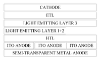
- the OLED drives a plurality of organic light emitting diodes to display an image, the organic light emitting diode includes an anode, an organic thin layer and a cathode.
- the organic thin layer usually has a multilayer structure including a light emitting layer (EML), an electron transport layer (ETL) and a hole transport layer (HTL), to improve the balance between electrons and holes, thereby improving luminescent efficiency.
- the multilayer structure may further include an electron injection layer (EIL) and a hole injection layer (HIL).
- red (R), green (G) and blue (B) light emitting layers may be patterned respectively.
- a shadow mask may be used in a case of a small-molecule OLED, and an inkjet printing method or a laser induced thermal imaging (LITI) method may be used in a case of a polymer OLED.
- LITI laser induced thermal imaging
- an organic layer may be finely patterned.
- the LITI method may be used for a large area, and an advantage of LITI method is a high resolution.
- a display with high pixels per inch (PPI) is a major trend of the current display device.
- FIG. 1 firstly, light emitting layers of sub-pixels of two colors, for example, R and G, are made simultaneously; then by using different optical thicknesses of the light emitting layers of the two sub-pixels, one of the colors, for example, R or G, is extracted by a micro-cavity effect; after that, when making a light emitting layer of a third color sub-pixel, the light emitting layer of the third color for example, B, may be formed in the entire pixel region.
- the OLED made in this manner along with the perspective being changed, a color cast is very serious, and the luminescent efficiency of the light emitting layers of the two colors manufactured simultaneously may also be decreased.
- One technical problem to be solved by the present disclosure is to provide an OLED display panel, a method for manufacturing the same, a display device and an electronic product, which can enhance a pixel density of an OLED display panel without changing the FMM accuracy.
- one embodiment of the present disclosure provides technical solutions as follows.
- an OLED display panel is provided.
- One pixel of the OLED display panel includes a first sub-pixel, a second sub-pixel and a third sub-pixel displaying different colors.
- the OLED display panel sequentially includes:
- a first light emitting layer covering at least two adjacent sub-pixels including the first sub-pixel
- a third light emitting layer covering at least two adjacent sub-pixels including the third sub-pixel
- LUMO energy levels of a main material of the charge blocking layer, a main light emitting material of the third light emitting layer, a main light emitting material of the second light emitting layer and a main light emitting material of the first light emitting layer are sequentially decreased;
- HOMO energy levels of the main light emitting material of the first light emitting layer, the main light emitting material of the second light emitting layer, the main light emitting material of the third light emitting layer and the main material of the charge blocking layer are sequentially decreased.
- the OLED display panel sequentially includes:
- the second light emitting layer covering the first sub-pixel and the second sub-pixel
- the third light emitting layer covering the entire pixel.
- the OLED display panel sequentially includes:
- the second light emitting layer covering the first sub-pixel and the second sub-pixel
- the third light emitting layer covering the second sub-pixel and the third sub-pixel.
- the OLED display panel sequentially includes:
- the first light emitting layer covering the first sub-pixel and the second sub-pixel
- the second light emitting layer covering the first sub-pixel and the second sub-pixel
- the third light emitting layer covering the entire pixel.
- the OLED display panel includes:
- the OLED display panel includes:
- One embodiment of the present disclosure further provides a display device including the OLED display panel described above.
- One embodiment of the present disclosure further provides a method for manufacturing an OLED display panel, one pixel of the OLED display panel including a first sub-pixel, a second sub-pixel and a third sub-pixel displaying different colors respectively, wherein the method includes:
- first light emitting layer covering at least two adjacent sub-pixels including the first sub-pixel
- LUMO energy levels of a main material of the charge blocking layer, a main light emitting material of the third light emitting layer, a main light emitting material of the second light emitting layer and a main light emitting material of the first light emitting layer are sequentially decreased;
- HOMO energy levels of the main light emitting material of the first light emitting layer, the main light emitting material of the second light emitting layer, the main light emitting material of the third light emitting layer and the main material of the charge blocking layer are sequentially decreased.
- the method includes:
- the manufacturing method includes:
- One embodiment of the present disclosure further provides an electronic product including the display device described above.
- each of the first light emitting layer, the charge blocking layer, the second light emitting layer and the third light emitting layer covers at least two sub-pixels, so that when the light emitting layer is manufactured by using FMM, a minimum opening of the FMM may be at least as large as two sub-pixel regions, thereby enhancing the pixel density of the OLED display panel without changing the FMM.
- the OLED display panel according to one embodiment of the present disclosure does not rely on an optical effect to extract light of a certain color, so that the luminescent efficiency is not lost, and a color cast problem is not occurred.
- the OLED display panel according to one embodiment of the present disclosure does not need to change the arrangement sequence of sub-pixels, and thus the screen display is not affected.
- FIG. 1 is a schematic diagram showing an OLED display panel in the related art
- FIG. 2 is a schematic diagram showing manufacturing a light emitting layer by using FMM with a large opening in the related art
- FIG. 3 is a schematic diagram showing LUMO energy levels of each of light emitting layers and a charge blocking layer according to a first embodiment of the present disclosure
- FIG. 4 is a schematic diagram showing an OLED display panel according to the first embodiment of the present disclosure.
- FIG. 5 is a schematic diagram showing HOMO energy levels of each of light emitting layers and a charge blocking layer according to a second embodiment of the present disclosure
- FIG. 6 is a schematic diagram showing an OLED display panel according to the second embodiment of the present disclosure.
- One embodiment of the present disclosure provides an OLED display panel, a method for manufacturing the same, a display device and an electronic product, which may enhance a pixel density of an OLED display panel without changing the FMM accuracy.
- One embodiment of the present disclosure provides an OLED display panel.
- One pixel of the OLED display panel includes a first sub-pixel, a second sub-pixel and a third sub-pixel displaying different colors.
- the OLED display panel sequentially includes:
- a first light emitting layer covering at least two adjacent sub-pixels including the first sub-pixel
- a third light emitting layer covering at least two adjacent sub-pixels including the third sub-pixel.
- the lowest unoccupied molecular orbital (LUMO) (note: an orbital unoccupied by an electron with the lowest energy level is referred as the lowest unoccupied orbital) energy levels of a main material of the charge blocking layer, a main light emitting material of the third light emitting layer, a main light emitting material of the second light emitting layer and a main light emitting material of the first light emitting layer are sequentially decreased; or, the highest occupied molecular orbital (HOMO) (note: an orbital occupied by an electron with the highest energy level is referred as the highest occupied orbital) energy levels of the main light emitting material of the first light emitting layer, the main light emitting material of the second light emitting layer, the main light emitting material of the third light emitting layer and the main material of the charge blocking layer are sequentially decreased.
- HOMO the highest occupied molecular orbital
- each of the first light emitting layer, the charge blocking layer, the second light emitting layer and the third light emitting layer covers at least two sub-pixels, so that when the light emitting layer is manufactured by using FMM, a minimum opening of the FMM may be at least as large as two sub-pixel regions, thereby enhancing the pixel density of the OLED display panel without changing the FMM.
- the OLED display panel according to one embodiment of the present disclosure does not rely on an optical effect to extract light of a certain color, so that the luminescent efficiency is not lost, and a color cast problem is also not occurred.
- the OLED display panel according to one embodiment of the present disclosure does not need to change the arrangement sequence of sub-pixels, and the screen display is not affected.
- the OLED display panel may sequentially include:
- the second light emitting layer covering the first sub-pixel and the second sub-pixel
- the third light emitting layer covering the entire pixel.
- the OLED display panel may sequentially include:
- the second light emitting layer covering the first sub-pixel and the second sub-pixel
- the third light emitting layer covering the second sub-pixel and the third sub-pixel.
- the OLED display panel may sequentially include:
- the first light emitting layer covering the first sub-pixel and the second sub-pixel
- the second light emitting layer covering the first sub-pixel and the second sub-pixel
- the OLED display panel may sequentially include:
- the first light emitting layer covering the first sub-pixel and the second sub-pixel
- the second light emitting layer covering the first sub-pixel and the second sub-pixel
- the third light emitting layer covering the entire pixel.
- the OLED display panel may specifically include:
- the OLED display panel may specifically include:
- the metal cathode layer on the electron transport layer is the metal cathode layer on the electron transport layer.
- the anode layer is set to be made of a semi-transparent material (e.g., indium tin oxide (ITO)) while the cathode layer is made of a metal, however, the embodiment of the present disclosure is not limited thereto. It should also be understood by those skilled in the art that the anode layer may be made of a metal and the cathode layer may be made of an ITO. Further, the following embodiment takes an example in which three sub-pixels are provided with anodes separately and share one cathode for illustration. However, those skilled in the art should understand that as an alternative, the three sub-pixels may share one anode and use separate cathodes for their own.
- a semi-transparent material e.g., indium tin oxide (ITO)
- ITO indium tin oxide
- One embodiment of the present disclosure further provides a display device, including the OLED display panel as described above.
- the structure and the working principle of the OLED display panel are as same as that in the above-described embodiment which will be omitted here. Further, the structure of the rest of the display device may refer to the related art, which will not be described in detail herein.
- the display device may be a product or component having any display function, such as an electronic paper, a TV, a monitor, a digital photo frame, a mobile phone, a tablet computer and the like.
- One embodiment of the present disclosure also provides a method for manufacturing an OLED display panel.
- One pixel of the OLED display panel includes a first sub-pixel, a second sub-pixel and a third sub-pixel displaying different colors.
- the manufacturing method includes:
- first light emitting layer covering at least two adjacent sub-pixels including the first sub-pixel
- Energy levels of LUMOs of a main material of the charge blocking layer, a main light emitting material of the third light emitting layer, a main light emitting material of the second light emitting layer and a main light emitting material of the first light emitting layer are sequentially decreased; or, energy levels of HOMOs of the main light emitting material of the first light emitting layer, the main light emitting material of the second light emitting layer, the main light emitting material of the third light emitting layer and the main material of the charge blocking layer are sequentially decreased.
- each of the first light emitting layer, the charge blocking layer, the second light emitting layer and the third light emitting layer covers at least two sub-pixels, so that when the light emitting layer is manufactured by using FMM, a minimum opening of the FMM may be at least as large as two sub-pixel regions, thereby enhancing the pixel density of the OLED display panel without changing the FMM.
- the OLED display panel according to one embodiment of the present disclosure does not rely on an optical effect to extract light of a certain color, so that the luminescent efficiency is not lost, and a color cast problem is not occurred.
- the OLED display panel according to one embodiment of the present disclosure does not need to change the arrangement sequence of sub-pixels, and thus the screen display is not affected.
- the method may specifically include:
- the method may specifically include:
- one embodiment of the present disclosure also provides an electronic product, including the display device described above.
- the structure and the working principle of the electronic product are as same as the above-described embodiment, which will be omitted here. Further, the structure of the rest of the electronic product may refer to the related art, which will not be described in detail herein.
- the electronic product may be a product or a component having any display function, such as a home appliance, a communication equipment, an engineering equipment, an electronic entertainment product and the like.
- OLED display panel and the method for manufacturing the same according to the present disclosure will be described in detail hereinafter in conjunction with the specific embodiments.
- one pixel of the OLED display panel includes a first sub-pixel displaying red, a second sub-pixel displaying green and a third sub-pixel displaying blue.
- the OLED display panel sequentially includes:
- EML 1 a first light emitting layer covering at least two adjacent sub-pixels including the first sub-pixel and configured to emit red light
- CBL charge blocking layer
- EML 2 a second light emitting layer covering the first sub-pixel and the second sub-pixel and configured to emit green light
- a third light emitting layer covering at least two adjacent sub-pixels including the third sub-pixel and configured to emit blue light.
- FIG. 3 is a diagram showing the LUMO energy levels of each light emitting layer and the charge blocking layer according to the first embodiment of the present disclosure.
- An arrow direction in FIG. 3 indicates an absolute value of the energy level.
- the LUMO energy levels of the first light emitting layer, the second light emitting layer, the third light emitting layer and the charge blocking layer are all negative; the LUMO energy level of the first light emitting layer is lower than that of the second light emitting layer, the LUMO energy level of the second light emitting layer is lower than that of the third light emitting layer, the LUMO energy level of the third light emitting layer is lower than that of the charge blocking layer.
- the OLED display panel may include:
- a method for manufacturing an OLED display panel includes following steps of:
- the light emitting layer is very thin, electrons are more likely to move in a direction from the cathode layer to the anode layer, and are not likely to move transversely in a direction perpendicular to an electric field. Electrons are readily to jump from one light emitting layer with a higher LUMO energy level to one light emitting layer with a lower LUMO energy level, and are difficult to jump from one light emitting layer with a lower LUMO energy level to one light emitting layer with a higher LUMO energy level. When an electron remains in one light emitting layer and encounters with a hole, an exciton is formed and light is emitted. According to the above principle, in the OLED display panel shown in FIG.
- the electrons start from the cathode layer. Since the LUMO energy level of the EML 2 is higher than that of the EML 1 , thus the electrons may pass through the EML 2 to reach EML 1 , but cannot pass through HTL. The electrons stay in the EML 1 to excite the EML 1 to emit red light, so that the first sub-pixel displays red light.
- the electrons may pass through the EML 3 to reach EML 2 , but cannot pass through the CBL, electrons stay in the EML 2 to excite the EML 2 to emit green light, so that the second sub-pixel displays green light.
- the electrons since the LUMO energy level of the EML 3 is lower than that of the CBL, thus, the electrons cannot pass through the CBL, the electrons stay in the EML 3 to excite the EML 3 to emit blue light, so that the third sub-pixel displays blue light.
- each of the first light emitting layer, the charge blocking layer, the second light emitting layer and the third light emitting layer covers at least two sub-pixels, so that when the light emitting layer is manufactured by using FMM, a minimum opening of the FMM may be at least as large as two sub-pixel regions, thereby enhancing the pixel density of the OLED display panel by twice without changing the FMM.
- the OLED display panel according to one embodiment of the present disclosure does not rely on an optical effect to extract light of a certain color, so that the luminescent efficiency is not lost, and a color cast problem is not occurred.
- the OLED display panel according to one embodiment of the present disclosure does not need to change the arrangement sequence of sub-pixels, and thus the screen display is not affected.
- the OLED display panel is not limited to the structure shown in FIG. 4 , instead of covering the entire pixel, the first light emitting layer may also cover only the first sub-pixel and the second sub-pixel; instead of covering the second sub-pixel and the third sub-pixel, the third light emitting layer may also cover the entire pixel.
- the second light emitting layer may only cover the first sub-pixel and the second sub-pixel, and the charge blocking layer may only cover the second sub-pixel and the third sub-pixel.
- the first sub-pixel is not limited to display red
- the second sub-pixel is not limited to display green
- the third sub-pixel is not limited to display blue, as long as the first sub-pixel, the second sub-pixel and the third sub-pixel display different colors, and each displays one of the red, green and blue.
- one pixel of the OLED display panel includes a first sub-pixel displaying red, a second sub-pixel displaying green and a third sub-pixel displaying blue.
- the OLED display panel sequentially includes:
- EML 1 a first light emitting layer covering at least two adjacent sub-pixels including the first sub-pixel and configured to emit red light
- CBL charge blocking layer
- EML 2 a second light emitting layer covering the first sub-pixel and the second sub-pixel and configured to emit green light
- a third light emitting layer covering at least two adjacent sub-pixels including the third sub-pixel and configured to emit blue light.
- FIG. 5 is a diagram showing HOMO energy levels of each light emitting layer and the charge blocking layer according to the second embodiment of the present disclosure.
- An arrow direction in FIG. 5 indicates an absolute value of the energy level.
- HOMO energy levels of the first light emitting layer, the second light emitting layer, the third light emitting layer and the charge blocking layer are all negative; the HOMO energy level of the first light emitting layer is higher than that of the second light emitting layer, the HOMO energy level of the second light emitting layer is higher than that of the third light emitting layer, the HOMO energy level of the third light emitting layer is higher than that of the charge blocking layer.
- the OLED display panel may include:
- a method for manufacturing an OLED display panel includes steps of:
- the light emitting layer is very thin, holes are more likely to move in a direction from the anode layer to the cathode layer, and are not likely to move transversely in a direction perpendicular to the electric field.
- the holes are readily to jump from one light emitting layer with a lower HOMO energy level to one light emitting layer with a higher HOMO energy level, and are difficult to jump from one light emitting layer with a higher HOMO energy level to one light emitting layer with a lower HOMO energy level.
- the holes start from the anode layer. Since the HOMO energy level of the EML 2 is lower than that of the EML 1 , thus the holes may pass through the EML 2 to reach EML 1 , but cannot pass through the ETL, the holes stay in the EML 1 to excite the EML 1 to emit red light, so that the first sub-pixel displays red light.
- the holes may pass through the EML 3 to reach EML 2 , but cannot pass through the CBL, holes stay in the EML 2 to excite the EML 2 to emit green light, so that the second sub-pixel displays green light.
- the HOMO energy level of the EML 3 is higher than that of the CBL, thus the holes cannot pass through the CBL, holes stay in the EML 3 to excite the EML 3 to emit blue light, so that the third sub-pixel displays blue light.
- each of the first light emitting layer, the charge blocking layer, the second light emitting layer and the third light emitting layer covers at least two sub-pixels, so that when the light emitting layer is manufactured by using FMM, a minimum opening of the FMM may be at least as large as two sub-pixel regions, thereby enhancing the pixel density of the OLED display panel by twice without changing the FMM.
- the OLED display panel according to one embodiment of the present disclosure does not rely on an optical effect to extract light of a certain color, so that the luminescent efficiency is not lost, and a color cast problem is not occurred.
- the OLED display panel according to one embodiment of the present disclosure does not need to change the arrangement sequence of sub-pixels, and thus the screen display is not affected.
- the OLED display panel is not limited to the structure shown in FIG. 6 , instead of covering the entire pixel, the first light emitting layer may also cover only the first sub-pixel and the second sub-pixel; instead of covering the second sub-pixel and the third sub-pixel, the third light emitting layer may also cover the entire pixel.
- the second light emitting layer may only cover the first sub-pixel and the second sub-pixel, and the charge blocking layer may only cover the second sub-pixel and the third sub-pixel.
- the first sub-pixel is not limited to display red
- the second sub-pixel is not limited to display green
- the third sub-pixel is not limited to display blue, as long as the first sub-pixel, the second sub-pixel and the third sub-pixel display different colors, and each displays one of the red, green and blue.
Applications Claiming Priority (4)
| Application Number | Priority Date | Filing Date | Title |
|---|---|---|---|
| CN201310669698.1A CN103824875B (zh) | 2013-12-10 | 2013-12-10 | Oled显示面板及其制作方法、显示装置 |
| CN201310669698 | 2013-12-10 | ||
| CN201310669698.1 | 2013-12-10 | ||
| PCT/CN2014/074155 WO2015085681A1 (zh) | 2013-12-10 | 2014-03-27 | Oled显示面板及其制作方法、显示装置、电子产品 |
Publications (2)
| Publication Number | Publication Date |
|---|---|
| US20160268351A1 US20160268351A1 (en) | 2016-09-15 |
| US9608044B2 true US9608044B2 (en) | 2017-03-28 |
Family
ID=50759837
Family Applications (1)
| Application Number | Title | Priority Date | Filing Date |
|---|---|---|---|
| US14/405,293 Active 2034-08-02 US9608044B2 (en) | 2013-12-10 | 2014-03-27 | OLED display panel, method for manufacturing the same, display device and electronic product |
Country Status (3)
| Country | Link |
|---|---|
| US (1) | US9608044B2 (zh) |
| CN (1) | CN103824875B (zh) |
| WO (1) | WO2015085681A1 (zh) |
Cited By (1)
| Publication number | Priority date | Publication date | Assignee | Title |
|---|---|---|---|---|
| US20160163772A1 (en) * | 2014-01-06 | 2016-06-09 | Boe Technology Group Co., Ltd. | Organic light-emitting diode (oled) display panel and display device |
Families Citing this family (9)
| Publication number | Priority date | Publication date | Assignee | Title |
|---|---|---|---|---|
| CN104617130A (zh) * | 2015-02-06 | 2015-05-13 | 京东方科技集团股份有限公司 | 一种oled像素单元、oled显示面板及显示装置 |
| CN104617231B (zh) * | 2015-02-06 | 2017-07-18 | 京东方科技集团股份有限公司 | 阵列基板及其制作方法、显示装置 |
| CN104733506B (zh) * | 2015-04-01 | 2017-10-24 | 京东方科技集团股份有限公司 | 一种电致发光显示器件及显示装置 |
| CN105226076B (zh) * | 2015-09-07 | 2018-03-27 | 深圳市华星光电技术有限公司 | 显示面板 |
| CN106229300B (zh) | 2016-08-23 | 2019-03-22 | 武汉华星光电技术有限公司 | 像素结构及制作方法 |
| US10181574B2 (en) | 2016-12-29 | 2019-01-15 | Lg Display Co., Ltd. | Organic light emitting device |
| US10418583B2 (en) * | 2017-02-27 | 2019-09-17 | Lg Display Co., Ltd. | Organic light emitting device |
| CN107170900B (zh) | 2017-05-12 | 2019-11-22 | 京东方科技集团股份有限公司 | Oled基板及其制备方法、显示装置 |
| CN109768178B (zh) * | 2019-01-22 | 2021-03-30 | 京东方科技集团股份有限公司 | 有机电致发光器件、显示基板、显示装置 |
Citations (10)
| Publication number | Priority date | Publication date | Assignee | Title |
|---|---|---|---|---|
| US20060238119A1 (en) | 2005-04-25 | 2006-10-26 | Eastman Kodak Company | Multicolor OLED displays |
| US20070046195A1 (en) | 2005-08-31 | 2007-03-01 | Univision Technology Inc. | Organic light-emitting display and fabricating method thereof |
| US20070046185A1 (en) * | 2005-08-26 | 2007-03-01 | Kim Byung H | Organic light emitting display and method for fabricating the same |
| US20080238300A1 (en) * | 2007-04-02 | 2008-10-02 | Sang Tae Park | Organic electroluminescence device and method for fabricating the same |
| US20100090241A1 (en) * | 2008-10-14 | 2010-04-15 | Universal Display Corporation | Emissive layer patterning for oled |
| JP2011048962A (ja) | 2009-08-26 | 2011-03-10 | Canon Inc | 有機el表示装置 |
| CN102856507A (zh) | 2011-06-29 | 2013-01-02 | 三星显示有限公司 | 发光结构、包括发光结构的显示装置及其制造方法 |
| US20130140533A1 (en) * | 2011-12-05 | 2013-06-06 | Au Optronics Corp. | Pixel structure of electroluminescent display panel |
| US20130153881A1 (en) * | 2010-09-24 | 2013-06-20 | Hitachi, Ltd. | Organic light-emitting devices and light source systems |
| CN103779387A (zh) | 2014-01-06 | 2014-05-07 | 京东方科技集团股份有限公司 | Oled显示面板及显示装置 |
-
2013
- 2013-12-10 CN CN201310669698.1A patent/CN103824875B/zh active Active
-
2014
- 2014-03-27 WO PCT/CN2014/074155 patent/WO2015085681A1/zh active Application Filing
- 2014-03-27 US US14/405,293 patent/US9608044B2/en active Active
Patent Citations (10)
| Publication number | Priority date | Publication date | Assignee | Title |
|---|---|---|---|---|
| US20060238119A1 (en) | 2005-04-25 | 2006-10-26 | Eastman Kodak Company | Multicolor OLED displays |
| US20070046185A1 (en) * | 2005-08-26 | 2007-03-01 | Kim Byung H | Organic light emitting display and method for fabricating the same |
| US20070046195A1 (en) | 2005-08-31 | 2007-03-01 | Univision Technology Inc. | Organic light-emitting display and fabricating method thereof |
| US20080238300A1 (en) * | 2007-04-02 | 2008-10-02 | Sang Tae Park | Organic electroluminescence device and method for fabricating the same |
| US20100090241A1 (en) * | 2008-10-14 | 2010-04-15 | Universal Display Corporation | Emissive layer patterning for oled |
| JP2011048962A (ja) | 2009-08-26 | 2011-03-10 | Canon Inc | 有機el表示装置 |
| US20130153881A1 (en) * | 2010-09-24 | 2013-06-20 | Hitachi, Ltd. | Organic light-emitting devices and light source systems |
| CN102856507A (zh) | 2011-06-29 | 2013-01-02 | 三星显示有限公司 | 发光结构、包括发光结构的显示装置及其制造方法 |
| US20130140533A1 (en) * | 2011-12-05 | 2013-06-06 | Au Optronics Corp. | Pixel structure of electroluminescent display panel |
| CN103779387A (zh) | 2014-01-06 | 2014-05-07 | 京东方科技集团股份有限公司 | Oled显示面板及显示装置 |
Non-Patent Citations (2)
| Title |
|---|
| Chinese Office Action dated Jan. 29, 2015 regarding Application No. 201310669698.1, filed Dec. 10, 2013. Translation provided by Dragon Intellectual Property Law Firm. |
| Written Opinion of the International Searching Authority for international application No. PCT/CN2014/074155. |
Cited By (2)
| Publication number | Priority date | Publication date | Assignee | Title |
|---|---|---|---|---|
| US20160163772A1 (en) * | 2014-01-06 | 2016-06-09 | Boe Technology Group Co., Ltd. | Organic light-emitting diode (oled) display panel and display device |
| US9881976B2 (en) * | 2014-01-06 | 2018-01-30 | Boe Technology Group Co., Ltd. | Organic light-emitting diode (OLED) display panel and display device |
Also Published As
| Publication number | Publication date |
|---|---|
| US20160268351A1 (en) | 2016-09-15 |
| CN103824875B (zh) | 2015-07-08 |
| CN103824875A (zh) | 2014-05-28 |
| WO2015085681A1 (zh) | 2015-06-18 |
Similar Documents
| Publication | Publication Date | Title |
|---|---|---|
| US9608044B2 (en) | OLED display panel, method for manufacturing the same, display device and electronic product | |
| US11665918B2 (en) | Organic light emitting device having an optical distance of a micro cavity and method of fabricating the same | |
| US8791454B2 (en) | Organic light emitting diode device and method of manufacturing the same | |
| JP4587852B2 (ja) | 有機電界発光素子及びその製造方法 | |
| US10002911B2 (en) | Display back plate and fabricating method thereof and display device | |
| US8227816B2 (en) | Organic light emitting display device | |
| US9881976B2 (en) | Organic light-emitting diode (OLED) display panel and display device | |
| KR101254748B1 (ko) | 유기전계발광표시장치 및 이의 제조방법 | |
| US9076978B2 (en) | Organic light emitting diode device | |
| KR20150006605A (ko) | 유기 발광 표시 장치 및 유기 발광 표시 장치의 제조 방법 | |
| KR102615126B1 (ko) | 마이크로 캐비티 구조를 갖는 유기전계발광표시장치 | |
| KR20120047799A (ko) | 표시 장치, 표시 장치의 제조 방법 및 전자기기 | |
| KR102146367B1 (ko) | 유기 발광 장치 | |
| KR20150080334A (ko) | 유기전계발광표시장치 | |
| CN104617130A (zh) | 一种oled像素单元、oled显示面板及显示装置 | |
| US8878168B2 (en) | Organic light-emitting display device with improved color property | |
| CN102969452A (zh) | 有机电致发光显示面板及其制造方法 | |
| KR20160037778A (ko) | 유기 발광 소자 | |
| KR20130024712A (ko) | 유기 전계 발광 표시 패널 및 그의 제조 방법 | |
| CN113659092A (zh) | 显示基板及显示装置 | |
| KR102473029B1 (ko) | 유기 발광 소자 | |
| KR20160038480A (ko) | 유기 발광 소자 | |
| CN107507917B (zh) | 一种oled器件及其制备方法、显示装置 | |
| JP2010060826A (ja) | 発光表示装置 | |
| KR100768230B1 (ko) | 유기 발광 표시소자 |
Legal Events
| Date | Code | Title | Description |
|---|---|---|---|
| AS | Assignment |
Owner name: BOE TECHNOLOGY GROUP CO., LTD., CHINA Free format text: ASSIGNMENT OF ASSIGNORS INTEREST;ASSIGNOR:WU, CHANGYEN;REEL/FRAME:034523/0915 Effective date: 20141104 |
|
| STCF | Information on status: patent grant |
Free format text: PATENTED CASE |
|
| MAFP | Maintenance fee payment |
Free format text: PAYMENT OF MAINTENANCE FEE, 4TH YEAR, LARGE ENTITY (ORIGINAL EVENT CODE: M1551); ENTITY STATUS OF PATENT OWNER: LARGE ENTITY Year of fee payment: 4 |