US9601553B2 - Organic light-emitting display and method of manufacturing the same - Google Patents

Organic light-emitting display and method of manufacturing the same Download PDF

Info

Publication number
US9601553B2
US9601553B2 US13/244,120 US201113244120A US9601553B2 US 9601553 B2 US9601553 B2 US 9601553B2 US 201113244120 A US201113244120 A US 201113244120A US 9601553 B2 US9601553 B2 US 9601553B2
Authority
US
United States
Prior art keywords
electrode
organic light
layer
pixel electrode
emitting display
Prior art date
Legal status (The legal status is an assumption and is not a legal conclusion. Google has not performed a legal analysis and makes no representation as to the accuracy of the status listed.)
Active, expires
Application number
US13/244,120
Other versions
US20120267670A1 (en
Inventor
June-Woo Lee
Jong-Moo Huh
Joon-hoo Choi
Current Assignee (The listed assignees may be inaccurate. Google has not performed a legal analysis and makes no representation or warranty as to the accuracy of the list.)
Samsung Display Co Ltd
Original Assignee
Samsung Display Co Ltd
Priority date (The priority date is an assumption and is not a legal conclusion. Google has not performed a legal analysis and makes no representation as to the accuracy of the date listed.)
Filing date
Publication date
Application filed by Samsung Display Co Ltd filed Critical Samsung Display Co Ltd
Assigned to SAMSUNG MOBILE DISPLAY CO., LTD. reassignment SAMSUNG MOBILE DISPLAY CO., LTD. ASSIGNMENT OF ASSIGNORS INTEREST (SEE DOCUMENT FOR DETAILS). Assignors: CHOI, JOON-HOO, HUH, JONG-MOO, LEE, JUNE-WOO
Publication of US20120267670A1 publication Critical patent/US20120267670A1/en
Application granted granted Critical
Publication of US9601553B2 publication Critical patent/US9601553B2/en
Assigned to SAMSUNG DISPLAY CO., LTD. reassignment SAMSUNG DISPLAY CO., LTD. MERGER (SEE DOCUMENT FOR DETAILS). Assignors: SAMSUNG MOBILE DISPLAY CO., LTD.
Active legal-status Critical Current
Adjusted expiration legal-status Critical

Links

Images

Classifications

    • HELECTRICITY
    • H05ELECTRIC TECHNIQUES NOT OTHERWISE PROVIDED FOR
    • H05BELECTRIC HEATING; ELECTRIC LIGHT SOURCES NOT OTHERWISE PROVIDED FOR; CIRCUIT ARRANGEMENTS FOR ELECTRIC LIGHT SOURCES, IN GENERAL
    • H05B33/00Electroluminescent light sources
    • H05B33/12Light sources with substantially two-dimensional radiating surfaces
    • H05B33/26Light sources with substantially two-dimensional radiating surfaces characterised by the composition or arrangement of the conductive material used as an electrode
    • H01L27/3265
    • HELECTRICITY
    • H01ELECTRIC ELEMENTS
    • H01LSEMICONDUCTOR DEVICES NOT COVERED BY CLASS H10
    • H01L33/00Semiconductor devices having potential barriers specially adapted for light emission; Processes or apparatus specially adapted for the manufacture or treatment thereof or of parts thereof; Details thereof
    • H01L33/44Semiconductor devices having potential barriers specially adapted for light emission; Processes or apparatus specially adapted for the manufacture or treatment thereof or of parts thereof; Details thereof characterised by the coatings, e.g. passivation layer or anti-reflective coating
    • H01L33/46Reflective coating, e.g. dielectric Bragg reflector
    • H01L33/465Reflective coating, e.g. dielectric Bragg reflector with a resonant cavity structure
    • HELECTRICITY
    • H10SEMICONDUCTOR DEVICES; ELECTRIC SOLID-STATE DEVICES NOT OTHERWISE PROVIDED FOR
    • H10KORGANIC ELECTRIC SOLID-STATE DEVICES
    • H10K59/00Integrated devices, or assemblies of multiple devices, comprising at least one organic light-emitting element covered by group H10K50/00
    • H10K59/10OLED displays
    • H10K59/12Active-matrix OLED [AMOLED] displays
    • H10K59/121Active-matrix OLED [AMOLED] displays characterised by the geometry or disposition of pixel elements
    • H10K59/1216Active-matrix OLED [AMOLED] displays characterised by the geometry or disposition of pixel elements the pixel elements being capacitors
    • H01L51/5215
    • H01L51/5218
    • HELECTRICITY
    • H10SEMICONDUCTOR DEVICES; ELECTRIC SOLID-STATE DEVICES NOT OTHERWISE PROVIDED FOR
    • H10KORGANIC ELECTRIC SOLID-STATE DEVICES
    • H10K50/00Organic light-emitting devices
    • H10K50/80Constructional details
    • H10K50/805Electrodes
    • H10K50/81Anodes
    • H10K50/816Multilayers, e.g. transparent multilayers
    • HELECTRICITY
    • H10SEMICONDUCTOR DEVICES; ELECTRIC SOLID-STATE DEVICES NOT OTHERWISE PROVIDED FOR
    • H10KORGANIC ELECTRIC SOLID-STATE DEVICES
    • H10K50/00Organic light-emitting devices
    • H10K50/80Constructional details
    • H10K50/805Electrodes
    • H10K50/81Anodes
    • H10K50/818Reflective anodes, e.g. ITO combined with thick metallic layers
    • HELECTRICITY
    • H10SEMICONDUCTOR DEVICES; ELECTRIC SOLID-STATE DEVICES NOT OTHERWISE PROVIDED FOR
    • H10KORGANIC ELECTRIC SOLID-STATE DEVICES
    • H10K59/00Integrated devices, or assemblies of multiple devices, comprising at least one organic light-emitting element covered by group H10K50/00
    • H10K59/80Constructional details
    • H10K59/805Electrodes
    • H10K59/8051Anodes
    • H10K59/80518Reflective anodes, e.g. ITO combined with thick metallic layers

Definitions

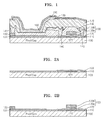
  • the organic light-emitting display may further include a source/drain electrode connected to the pixel electrode, an active layer connected to the source/drain electrode, and the gate electrode disposed to face the active layer.

Landscapes

  • Engineering & Computer Science (AREA)
  • Microelectronics & Electronic Packaging (AREA)
  • Physics & Mathematics (AREA)
  • Geometry (AREA)
  • Manufacturing & Machinery (AREA)
  • Computer Hardware Design (AREA)
  • Power Engineering (AREA)
  • Electroluminescent Light Sources (AREA)

Abstract

An organic light-emitting display having an improved aperture ratio, the organic light-emitting display including a rear electrode, an opposite electrode, and a pixel electrode between the rear electrode and the opposite electrode. Here, an insulating layer is interposed between the pixel electrode and the rear electrode, wherein the pixel electrode, the insulating layer, and the rear electrode are configured as a capacitor of the organic light-emitting display. In such a structure, as the capacitor is disposed in a light-emitting area where the pixel electrode exists, it is not necessary to provide an additional space for a capacitor, thus improving an aperture ratio of the display.

Description

CROSS-REFERENCE TO RELATED APPLICATION
This application claims priority to and the benefit of Korean Patent Application No. 10-2011-0037985, filed on Apr. 22, 2011, in the Korean Intellectual Property Office, the entire content of which is incorporated herein by reference.
BACKGROUND
1. Field
The following description relates to an organic light-emitting display, and more particularly, to an organic light-emitting display having an improved aperture ratio and a method of manufacturing the organic light-emitting display.
2. Description of Related Art
An active matrix organic light-emitting display which has recently attracted a lot of attention includes a thin-film transistor (TFT), a capacitor, and an organic light-emitting diode (OLED) connected to the TFT and the capacitor, in each pixel. The OLED emits light and forms a desired image by receiving an appropriate driving signal from the TFT and the capacitor.
In addition, the capacitor needs to have a sufficient capacity so that the organic light-emitting display more stably displays an image. In other words, a sufficient charging capacity of the capacitor may ensure more natural images. However, an enlargement of the capacitor so as to increase the charging capacity thereof may cause a decrease in a light-emitting area of the OLED, that is, a decrease in an aperture ratio, thereby leading to a decrease in the brightness of the OLED. Accordingly, proper measures need to be taken to prevent or counter this problem.
SUMMARY
Aspects of embodiments of the present invention are directed toward an organic light-emitting display capable of preventing a reduction in an aperture ratio due to the enlargement of a capacitor, and a method of manufacturing the organic light-emitting display.
According to an embodiment of the present invention, there is provided an organic light-emitting display including a pixel electrode; an opposite electrode facing a first side of the pixel electrode; an organic light emission layer interposed between the first side of the pixel electrode and the opposite electrode; a rear electrode facing a second side of the pixel electrode, the second side facing oppositely away from the first side; and an insulating layer interposed between the pixel electrode and the rear electrode, wherein the pixel electrode, the insulating layer, and the rear electrode are configured as a capacitor of the organic light-emitting display.
The pixel electrode and the rear electrode may each be a translucent electrode.
The translucent electrode may have a structure of interposing a silver alloy layer between indium tin oxide (ITO) layers.
The organic light-emitting display may further include a source/drain electrode connected to the pixel electrode, an active layer connected to the source/drain electrode, and the gate electrode disposed to face the active layer.
The gate electrode may include a translucent electrode layer formed on the same layer as the rear electrode and a low-resistance electrode layer formed on the translucent electrode layer.
The organic light-emitting display may further include a capacitor wiring connected to the rear electrode, wherein the capacitor wiring may include a first wiring layer formed on the same layer as the low-electrode layer and connected to the rear electrode, and a second wiring layer formed on the same layer as the source/drain electrode and connected to the first wiring layer.
The rear electrode may be a split electrode divided into several portions each forming a separate capacitor.
According to another embodiment of the present invention, there is provided a method of manufacturing an organic light-emitting display, the method including forming an active layer on a substrate; forming a gate electrode on a first insulating layer disposed on the active layer and forming a rear electrode on the same layer as the gate electrode; forming a second insulating layer having a contact hole, on the gate electrode and the rear electrode; forming a source/drain electrode connected to the active layer and a capacitor wiring connected to the rear electrode through the contact hole; forming a pixel electrode, which faces the rear electrode having the second insulating layer therebetween, so that the pixel electrode is connected to the source/drain electrode; forming an organic light emission layer on the pixel electrode; and forming an opposite electrode facing the pixel electrode having the organic light emission layer therebetween.
The pixel electrode and the rear electrode may each be a translucent electrode.
The translucent electrode may have a structure of interposing a silver alloy layer between indium tin oxide (ITO) layers.
The gate electrode may include a translucent electrode layer formed on the same layer as the rear electrode and a low-resistance electrode layer formed on the translucent electrode layer.
The capacitor wiring may include a first wiring layer formed on the same layer as the low-resistance electrode layer and connected to the rear electrode and a second wiring layer formed on the same layer as the source/drain electrode and connected to the first wiring layer.
The rear electrode is formed of split electrodes respectively forming separate capacitors.
BRIEF DESCRIPTION OF THE DRAWINGS
The above and other features and advantages of the present invention will become more apparent by describing in detail exemplary embodiments thereof with reference to the attached drawings in which:
FIG. 1 is a cross-sectional view of an organic light-emitting display according to an embodiment of the present invention;
FIGS. 2A through 2F are cross-sectional views illustrating a method of manufacturing the organic light-emitting display of FIG. 1, according to an embodiment of the present invention; and
FIG. 3 is a cross-sectional view of an organic light-emitting display according to another embodiment of the present invention.
DETAILED DESCRIPTION
Hereinafter, exemplary embodiments of the present invention will be described fully with reference to the accompanying drawings.
FIG. 1 is a cross-sectional view of an organic light-emitting display according to an embodiment of the present invention, which is a bottom emission type organic light-emitting display. Although FIG. 1 illustrates a pixel of the organic light-emitting display, the organic light-emitting display includes a plurality of the pixels.
Referring to FIG. 1, the organic light-emitting display according to the current embodiment includes a thin-film transistor unit TFT and a pixel/capacitor unit Pixel/Cap which are formed on a substrate 100 and are electrically connected with each other. The thin-film transistor unit TFT is connected to a pixel electrode 160 of the pixel/capacitor unit Pixel/Cap to supply an appropriate current for light emission. The pixel/capacitor unit Pixel/Cap illuminates an organic light emission layer 180 based on the current supplied from the thin-film transistor unit TFT to form an image and also performs charging (e.g., performs charge storing and discharging) as a capacitor. That is, in the current embodiment, the pixel electrode 160 of the pixel/capacitor unit Pixel/Cap is used as an electrode for illuminating the organic light emission layer 180 and also used as an electrode for charging as a capacitor. Accordingly, no special capacitors need to be included, which may help to obtain a sufficient aperture ratio. Therefore, high resolution images may be displayed.
Hereinafter, a detailed structure of the organic light-emitting display having such a feature will be described.
The thin-film transistor unit TFT includes an active layer 110 formed on the substrate 100, a gate electrode 130 formed to face the active layer 110 by interposing a first insulating layer 120 between the active layer 110 and the gate electrode 130, and source/drain electrodes 140, one of which is connected to the pixel electrode 160 of the pixel/capacitor unit Pixel/Cap via the active layer 110. Accordingly, when a proper voltage is applied to the gate electrode 130, the active layer 110 may enter into a state where a current can flow, and thus, a current may be supplied to the pixel electrode 160 which is connected to one of the source/drain electrodes 140.
The gate electrode 130 may be formed to have a multi-layered structure in which a low-resistance electrode layer 130 b such as molybdenum may be stacked on a translucent electrode layer 130 a obtained by interposing a silver alloy layer between indium tin oxide (ITO) layers, for example. The translucent electrode layer 130 a is formed of the same material and of the same layer as a rear electrode 131 for a capacitor, which will be explained below. The low-resistance electrode layer 130 b is formed of a relatively low-resistance material for smooth transmission of a gate signal.
The pixel/capacitor unit Pixel/Cap includes the rear electrode 131, the pixel electrode 160, an opposite electrode 190, and the organic light emission layer 180. The rear electrode 131 is formed of the same material and of the same layer as the translucent electrode layer 130 a of the gate electrode 130, i.e., on the first insulating layer 120. The pixel electrode 160 faces the rear electrode 131 with a second insulating layer 150 therebetween, and is connected to one of the source/drain electrodes 140. The opposite electrode 190 faces the pixel electrode 160, and the organic light emission layer 180 is interposed between the pixel electrode 160 and the opposite electrode 190. Accordingly, when an electric current is supplied to the pixel electrode 160 via the source/drain electrode 140 of the thin-film transistor unit TFT, light is emitted from the organic light emission layer 180, thus forming an image. The pixel electrode 160 and the rear electrode 131 also function as a capacitor. The pixel electrode 160 and the rear electrode 131 form a structure of a capacitor by facing each other with the second insulating layer 150 therebetween. Accordingly, the pixel electrode 160 and the rear electrode 131 may also function as a capacitor in a portion of the generated illumination. Furthermore, in the current embodiment, the pixel electrode 160 may also be formed of a translucent electrode obtained by interposing a silver alloy layer between ITO layers. When the pixel electrode 160 and the rear electrode 131 are formed as translucent electrodes, light emitted from the organic light emission layer 180 generates a micro cavity between the pixel electrode 160 and the opposite electrode 190, thus obtaining stronger light. That is, when the light emitted from the organic light emission layer 180 shuttles between the pixel electrode 160 and the rear electrode 131, which are translucent electrodes, constructive or destructive interference occurs, thus strengthening or destroying an intensity of the light. Therefore, stronger light may be obtained by properly adjusting a space between the pixel electrode 160 and the rear electrode 131 so that light results in constructive interference.
Reference numerals 132 and 141 denote capacitor wirings connected to the rear electrode 131. The reference numeral 132 denotes a first wiring layer formed of the same layer as the low-resistance electrode layer 130 b of the gate electrode 130. The reference numeral 141 denotes a second wiring layer formed of the same layer as the source/drain electrodes 140. A reference numeral 170 denotes a pixel-defining film.
The organic light-emitting display having the structure described above may be manufactured by following a method illustrated in FIGS. 2A through 2F.
FIGS. 2A through 2F are cross-sectional views illustrating a method of manufacturing the organic light-emitting display of FIG. 1, according to an embodiment of the present invention.
As illustrated in FIG. 2A, the active layer 110 is formed in the thin film transistor unit TFT on the substrate 100, and the first insulating layer 120 is formed on the active layer 110.
Next, as illustrated in FIG. 2B, a gate electrode 130 is formed on the active layer 110 of the thin-film transistor unit TFT to face the active layer 110. At the same time, the rear electrode 131 and the first wiring layer 132 (as a capacitor wiring) are formed of the same layer as the gate electrode 130, in the pixel/capacitor unit Pixel/Cap. That is, the translucent electrode layer 130 a of the gate electrode 130 and the rear electrode 131 are formed of the same layer, and the low-resistance electrode 130 b of the gate electrode 130 and the first wiring layer 132 (as a capacitor wiring) are formed of the same layer on the translucent electrode layer 130 a and the rear electrode 131, respectively.
Then, as illustrated in FIG. 2C, the second insulating layer 150 is formed. Contact holes 151 are also formed to expose the active layer 110 and the first wiring layer 132.
As illustrated in FIG. 2D, the source/drain electrodes 140 and the second wiring layer 141 are formed through the contact holes 151 so as to contact the active layer 110 and the first wiring layer 132, respectively.
Then, as illustrated in FIG. 2E, the pixel electrode 160 connected to the source drain electrodes 140 is formed to face the rear electrode 131. In this way, a structure of a capacitor including the pixel electrode 160 and the rear electrode 131 as two electrodes of the capacitor is formed.
Next, as illustrated in FIG. 2F, the organic light emission layer 180 is formed on the pixel electrode 160 which is defined in units of pixels by the pixel-defining film 170, and the opposite pixel 190 is formed on the organic light emission layer 180 (Refer to FIG. 1). Thus, a basic structure of the organic light-emitting display for performing light emission and charging according to a signal from the thin-film transistor unit TFT is formed. That is, light emission of the organic light emission layer 180 is generated between the pixel electrode 160 and the opposite electrode 190, while a capacitor is charged between the pixel electrode 160 and the rear electrode 190.
As the organic light-emitting display manufactured by such a method has both the capacitor and the pixel electrode 160 in a pixel portion, it is not necessary to provide an additional space for the capacitor, which may help to enhance an aperture ratio. Therefore, the organic light-emitting display may have an advantage in having high resolution. Furthermore, as the pixel electrode 160 and the rear electrode 131 are formed of translucent electrodes, the organic light-emitting display may also provide a structure which is very effective on generating a constructive interference of light by using a micro cavity.
FIG. 3 is a cross-sectional view of an organic light-emitting display according to another embodiment of the present invention.
The current embodiment illustrates a modification example in which the number of capacitors is increased. Like the previous embodiment, a pixel electrode 260 in the current embodiment is used for both light emission and charging.
Referring to a thin-film transistor unit TFT, an active layer 210, a first insulating layer 220, a gate electrode 230, and source/ drain electrodes 240 a, 240 b, and 240 c are formed on a substrate 200. The gate electrode 230 is formed to have a multi-layered structure formed by stacking a low-resistance electrode layer 230 b on a translucent electrode layer 230 a.
As illustrated in the cross-sectional view of FIG. 3, the source/drain electrode 240 b connected to the active layer 210 and the source/drain electrode 240 c connected to a pixel electrode 260 may seem to be electrically separate from each other. However, the source/drain electrode 240 c and the source/drain electrode 240 b are actually connected with each other.
Next, a pixel/capacitor unit Pixel/Cap includes a pair of rear electrodes 231 a and 231 b, the pixel electrode 260, an opposite electrode 290, and an organic light emission layer 280. The rear electrodes 231 a and 231 b are formed on a first insulating layer 220, of the same material and of the same layer as a translucent electrode layer 230 a of the gate electrode 230. The pixel electrode 260 faces the rear electrodes 231 a and 231 b with a second insulating layer 250 therebetween and is connected to the source/drain electrode 240 c. The opposite electrode 290 faces the pixel electrode 260, and the organic light emission layer 280 is interposed between the pixel electrode 260 and the opposite electrode 290.
Accordingly, when an electric current is supplied to the pixel electrode 260 via the source/ drain electrodes 240 a, 240 b, and 240 c of the thin-film transistor unit TFT, light emission is generated from the organic light emission layer 280, thus forming an image. The pixel electrode 260 and the rear electrodes 231 a and 231 b also function as a capacitor. That is, the pixel electrode 260 and the rear electrodes 231 a and 231 b face each other with a second insulating layer 250 therebetween, thereby forming a structure of one or more capacitors. As such, a function of a capacitor may be implemented in the light emission area.
Furthermore, in the current embodiment, the pixel electrode 260 and the rear electrodes 231 a and 231 b are formed of translucent electrodes obtained by interposing a silver alloy layer between indium tin oxide (ITO) layers. Therefore, light emitted from the organic light emission layer 280 may generate a micro cavity between the pixel electrode 260 and the opposite electrode 290, thus obtaining stronger light.
Reference numerals 232 a, 232 b, 241 a, and 241 b denote capacitor wirings connected to the rear electrode 231. The reference numerals 232 a and 232 b denote first wiring layers 232 a and 232 b formed of the same layer as the low-resistance electrode layer 230 b of the gate electrode 230. The reference numerals 241 a and 241 b denote second wiring layers 241 a and 241 b formed of the same layer as the source/ drain electrodes 240 a, 240 b, and 240 c. A reference numeral 270 denotes a pixel-defining film.
Accordingly, the organic light-emitting display according to the current embodiment may include two capacitors formed by depositing a pair of the rear electrodes 231 a and 231 b, and the two capacitors may be deposited in the pixel portion under the pixel electrode 260, thus enhancing an aperture ratio.
In addition, like the previous embodiment, as the pixel electrode 260 and the rear electrodes 231 a and 231 b are formed of translucent electrodes, an effect of constructive interference of light by using on a micro cavity may be used for obtaining stronger light.
The organic light-emitting displays according to the above-described embodiments of the present invention may provide a sufficient aperture ratio without having to reduce a capacitor, thus forming a stable high resolution image.
While the present invention has been particularly shown and described with reference to exemplary embodiments thereof, it will be understood by those of ordinary skill in the art that various changes in form and details may be made therein without departing from the spirit and scope of the present invention as defined by the following claims.

Claims (9)

What is claimed is:
1. An organic light-emitting display comprising:
a plurality of pixels, each pixel comprising:
a pixel electrode;
an opposite electrode facing a first side of the pixel electrode;
an organic light emission layer between the first side of the pixel electrode and the opposite electrode;
a rear electrode facing a second side of the pixel electrode, the second side facing oppositely away from the first side; and
an insulating layer between the second side of the pixel electrode and the rear electrode,
wherein the pixel electrode, the insulating layer, and the rear electrode are configured as a plurality of capacitors of the organic light-emitting display, and the pixel electrode overlaps with and is located between the organic light emission layer and the rear electrode,
wherein the rear electrode is a split electrode divided into several discontiguous portions each forming a separate capacitor of the plurality of capacitors, and
wherein the several discontiguous portions together extend from a first edge of the pixel electrode to a second edge of the pixel electrode facing away from the first edge, such that a micro cavity extends from the first edge to the second edge.
2. The organic light-emitting display of claim 1, wherein each of the pixel electrode and the rear electrode is a translucent electrode.
3. The organic light-emitting display of claim 2, wherein the translucent electrode has a structure in which a silver alloy layer is interposed between indium tin oxide (ITO) layers.
4. The organic light-emitting display of claim 1, further comprising:
source/drain electrodes, one of which is connected to the pixel electrode;
an active layer connected to the source/drain electrodes; and
a gate electrode facing the active layer.
5. The organic light-emitting display of claim 4, wherein the gate electrode comprises a translucent electrode layer formed of a same layer as the rear electrode and a low-resistance electrode layer formed on the translucent electrode layer.
6. The organic light-emitting display of claim 5, further comprising a capacitor wiring connected to the rear electrode,
wherein the capacitor wiring comprises a first wiring layer formed of a same layer as the low-resistance electrode layer and connected to the rear electrode and a second wiring layer formed of a same layer as the source/drain electrodes and connected to the first wiring layer.
7. The organic light-emitting display of claim 1, wherein the pixel electrode is configured with the rear electrode and the organic light emission layer to provide a micro cavity to construct an intensity of light emitted from the organic light emission layer.
8. An organic light-emitting display comprising:
a plurality of pixels, each pixel comprising:
a rear electrode;
an opposite electrode;
a pixel electrode between the rear electrode and the opposite electrode;
an organic light emission layer between the pixel electrode and the opposite electrode; and
an insulating layer between the pixel electrode and the rear electrode,
wherein the pixel electrode, the insulating layer, and the rear electrode are configured as a plurality of capacitors of the organic light-emitting display, and the pixel electrode is configured with the organic light emission layer and the opposite electrode as an organic light emitting diode (OLED) of the organic light-emitting display,
wherein the rear electrode is a split electrode divided into several discontiguous portions each forming a separate capacitor of the plurality of capacitors, and
wherein the several discontiguous portions together extend from a first edge of the pixel electrode to a second edge of the pixel electrode facing away from the first edge, such that a micro cavity extends from the first edge to the second edge.
9. The organic light-emitting display of claim 8, wherein the pixel electrode is configured with the rear electrode and the organic light emission layer to provide a micro cavity to construct an intensity of light emitted from the organic light emission layer.
US13/244,120 2011-04-22 2011-09-23 Organic light-emitting display and method of manufacturing the same Active 2034-12-29 US9601553B2 (en)

Applications Claiming Priority (2)

Application Number Priority Date Filing Date Title
KR1020110037985A KR101962850B1 (en) 2011-04-22 2011-04-22 An organic light emitting display device and the manufacturing method thereof
KR10-2011-0037985 2011-04-22

Publications (2)

Publication Number Publication Date
US20120267670A1 US20120267670A1 (en) 2012-10-25
US9601553B2 true US9601553B2 (en) 2017-03-21

Family

ID=47020615

Family Applications (1)

Application Number Title Priority Date Filing Date
US13/244,120 Active 2034-12-29 US9601553B2 (en) 2011-04-22 2011-09-23 Organic light-emitting display and method of manufacturing the same

Country Status (2)

Country Link
US (1) US9601553B2 (en)
KR (1) KR101962850B1 (en)

Families Citing this family (5)

* Cited by examiner, † Cited by third party
Publication number Priority date Publication date Assignee Title
US9012900B2 (en) * 2012-12-26 2015-04-21 Lg Display Co., Ltd. Organic light emitting diode display device and method of fabricating the same
KR102028990B1 (en) * 2012-12-26 2019-10-07 엘지디스플레이 주식회사 Organic light emitting diode display device and method for fabricating the same
KR102116493B1 (en) * 2013-05-23 2020-06-08 삼성디스플레이 주식회사 Organinc light emitting display device and manufacturing method for the same
CN104752464B (en) * 2013-12-27 2018-08-07 昆山国显光电有限公司 A kind of organic light-emitting display device and preparation method thereof
KR102166341B1 (en) * 2014-09-05 2020-10-16 엘지디스플레이 주식회사 Organic Light Emitting Diode Display Having High Aperture Ratio And Method For Manufacturing The Same

Citations (7)

* Cited by examiner, † Cited by third party
Publication number Priority date Publication date Assignee Title
US20050088081A1 (en) * 2003-09-30 2005-04-28 Sanyo Electric Co., Ltd. Organic electroluminescent device
US20070252145A1 (en) * 2006-04-28 2007-11-01 Yoshiaki Toyota Image display device and manufacturing method thereof
US20070278480A1 (en) * 2006-06-02 2007-12-06 Eui-Hoon Hwang Organic light emitting display and method of manufacturing the same
US20090141203A1 (en) * 2007-12-03 2009-06-04 Samsung Electronics Co., Ltd. Display devices including an oxide semiconductor thin film transistor
US20090284449A1 (en) 2008-05-19 2009-11-19 Hun-Jung Lee Organic light emitting display device
US20100182224A1 (en) * 2009-01-16 2010-07-22 Sony Corporation Display device and electronic apparatus
US20110140107A1 (en) 2009-12-10 2011-06-16 Jin-Hee Kang Flat panel display device and method of manufacturing the same

Family Cites Families (6)

* Cited by examiner, † Cited by third party
Publication number Priority date Publication date Assignee Title
KR100904261B1 (en) * 2002-12-06 2009-06-24 엘지디스플레이 주식회사 Liquid crystal display panel
KR20060067281A (en) * 2004-12-14 2006-06-19 엘지.필립스 엘시디 주식회사 Thin film transistor substrate and method for fabricating the same
KR100761077B1 (en) * 2005-05-12 2007-09-21 삼성에스디아이 주식회사 Organic electroluminescent display device
KR20070051031A (en) * 2005-11-14 2007-05-17 엘지전자 주식회사 Electronic paper display apparatus having multi-electrode and manufacturing process thereof
KR101322139B1 (en) * 2006-11-27 2013-10-25 엘지디스플레이 주식회사 Organic Light Emitting Device and Pixel Construction thereof
KR101058109B1 (en) * 2009-09-15 2011-08-24 삼성모바일디스플레이주식회사 Organic light emitting display device

Patent Citations (10)

* Cited by examiner, † Cited by third party
Publication number Priority date Publication date Assignee Title
US20050088081A1 (en) * 2003-09-30 2005-04-28 Sanyo Electric Co., Ltd. Organic electroluminescent device
US20070252145A1 (en) * 2006-04-28 2007-11-01 Yoshiaki Toyota Image display device and manufacturing method thereof
US20070278480A1 (en) * 2006-06-02 2007-12-06 Eui-Hoon Hwang Organic light emitting display and method of manufacturing the same
US20090141203A1 (en) * 2007-12-03 2009-06-04 Samsung Electronics Co., Ltd. Display devices including an oxide semiconductor thin film transistor
KR20090057689A (en) 2007-12-03 2009-06-08 삼성전자주식회사 Display device using oxide semiconductor thin film transistor
US20090284449A1 (en) 2008-05-19 2009-11-19 Hun-Jung Lee Organic light emitting display device
KR20090120093A (en) 2008-05-19 2009-11-24 삼성모바일디스플레이주식회사 Organic light emitting display device
US20100182224A1 (en) * 2009-01-16 2010-07-22 Sony Corporation Display device and electronic apparatus
US20110140107A1 (en) 2009-12-10 2011-06-16 Jin-Hee Kang Flat panel display device and method of manufacturing the same
KR20110065820A (en) 2009-12-10 2011-06-16 삼성모바일디스플레이주식회사 Flat panel display device and method of manufacturing the same

Also Published As

Publication number Publication date
KR20120119791A (en) 2012-10-31
KR101962850B1 (en) 2019-03-28
US20120267670A1 (en) 2012-10-25

Similar Documents

Publication Publication Date Title
CN109950278B (en) Electroluminescent display device
JP7157231B2 (en) Light-emitting device and display device provided with the same
CN109904191B (en) Electroluminescent display device
JP6676131B2 (en) Electroluminescent display
KR101983888B1 (en) Transparent oled device and display device employing same
KR101699911B1 (en) Organic light emitting diode display
US9312309B2 (en) Organic light emitting diode display and method for manufacturing the same
KR101939366B1 (en) Organic light emitting diode display
US8901563B2 (en) Organic light-emitting display device and method of manufacturing the same
US9997572B2 (en) Display device having a light scattering structure
US10680207B2 (en) Electroluminescent display device having reflective patterns within depressed portions
US9312321B2 (en) Double-sided organic light-emitting diode, and manufacturing method and display device thereof
EP3843142A1 (en) Light-emitting device, manufacturing method thereof, and display device having same
US9601553B2 (en) Organic light-emitting display and method of manufacturing the same
JP2022502712A (en) A light emitting device, a manufacturing method thereof, and a display device equipped with the light emitting device.
JP2018054728A (en) Display device
KR20140129852A (en) Organic light emitting diode display
KR20130093187A (en) Organic light emitting display device and method for manufacturing thereof
US9859339B2 (en) Display substrate, manufacturing method and driving method thereof, and display device
CN107146806B (en) OLED display substrate and OLED display device
KR20140111839A (en) Organic light emitting diode display
KR20160076066A (en) Light emitting display device
JP2012038631A (en) Organic electroluminescence display device
WO2016197524A1 (en) Organic electroluminescent display device, display apparatus, and manufacturing method therefor
US20070241672A1 (en) Organic electroluminescence display device

Legal Events

Date Code Title Description
AS Assignment

Owner name: SAMSUNG MOBILE DISPLAY CO., LTD., KOREA, REPUBLIC

Free format text: ASSIGNMENT OF ASSIGNORS INTEREST;ASSIGNORS:LEE, JUNE-WOO;HUH, JONG-MOO;CHOI, JOON-HOO;REEL/FRAME:026963/0283

Effective date: 20110923

FEPP Fee payment procedure

Free format text: PAYOR NUMBER ASSIGNED (ORIGINAL EVENT CODE: ASPN); ENTITY STATUS OF PATENT OWNER: LARGE ENTITY

STCF Information on status: patent grant

Free format text: PATENTED CASE

AS Assignment

Owner name: SAMSUNG DISPLAY CO., LTD., KOREA, REPUBLIC OF

Free format text: MERGER;ASSIGNOR:SAMSUNG MOBILE DISPLAY CO., LTD.;REEL/FRAME:042052/0671

Effective date: 20120702

MAFP Maintenance fee payment

Free format text: PAYMENT OF MAINTENANCE FEE, 4TH YEAR, LARGE ENTITY (ORIGINAL EVENT CODE: M1551); ENTITY STATUS OF PATENT OWNER: LARGE ENTITY

Year of fee payment: 4

MAFP Maintenance fee payment

Free format text: PAYMENT OF MAINTENANCE FEE, 8TH YEAR, LARGE ENTITY (ORIGINAL EVENT CODE: M1552); ENTITY STATUS OF PATENT OWNER: LARGE ENTITY

Year of fee payment: 8