US9601471B2 - Three layer stack structure - Google Patents
Three layer stack structure Download PDFInfo
- Publication number
- US9601471B2 US9601471B2 US14/804,261 US201514804261A US9601471B2 US 9601471 B2 US9601471 B2 US 9601471B2 US 201514804261 A US201514804261 A US 201514804261A US 9601471 B2 US9601471 B2 US 9601471B2
- Authority
- US
- United States
- Prior art keywords
- level
- die
- rdl
- molding compound
- encapsulated
- Prior art date
- Legal status (The legal status is an assumption and is not a legal conclusion. Google has not performed a legal analysis and makes no representation as to the accuracy of the status listed.)
- Active
Links
Images


Classifications
-
- H01L25/105—
-
- H—ELECTRICITY
- H10—SEMICONDUCTOR DEVICES; ELECTRIC SOLID-STATE DEVICES NOT OTHERWISE PROVIDED FOR
- H10W—GENERIC PACKAGES, INTERCONNECTIONS, CONNECTORS OR OTHER CONSTRUCTIONAL DETAILS OF DEVICES COVERED BY CLASS H10
- H10W90/00—Package configurations
-
- H01L25/50—
-
- H—ELECTRICITY
- H10—SEMICONDUCTOR DEVICES; ELECTRIC SOLID-STATE DEVICES NOT OTHERWISE PROVIDED FOR
- H10W—GENERIC PACKAGES, INTERCONNECTIONS, CONNECTORS OR OTHER CONSTRUCTIONAL DETAILS OF DEVICES COVERED BY CLASS H10
- H10W70/00—Package substrates; Interposers; Redistribution layers [RDL]
- H10W70/01—Manufacture or treatment
- H10W70/05—Manufacture or treatment of insulating or insulated package substrates, or of interposers, or of redistribution layers
- H10W70/08—Manufacture or treatment of insulating or insulated package substrates, or of interposers, or of redistribution layers by depositing layers on the chip or wafer, e.g. "chip-first" RDLs
- H10W70/09—Manufacture or treatment of insulating or insulated package substrates, or of interposers, or of redistribution layers by depositing layers on the chip or wafer, e.g. "chip-first" RDLs extending onto an encapsulation that laterally surrounds the chip or wafer, e.g. fan-out wafer level package [FOWLP] RDLs
-
- H—ELECTRICITY
- H10—SEMICONDUCTOR DEVICES; ELECTRIC SOLID-STATE DEVICES NOT OTHERWISE PROVIDED FOR
- H10W—GENERIC PACKAGES, INTERCONNECTIONS, CONNECTORS OR OTHER CONSTRUCTIONAL DETAILS OF DEVICES COVERED BY CLASS H10
- H10W70/00—Package substrates; Interposers; Redistribution layers [RDL]
- H10W70/60—Insulating or insulated package substrates; Interposers; Redistribution layers
- H10W70/611—Insulating or insulated package substrates; Interposers; Redistribution layers for connecting multiple chips together
- H10W70/614—Insulating or insulated package substrates; Interposers; Redistribution layers for connecting multiple chips together the multiple chips being integrally enclosed
-
- H—ELECTRICITY
- H10—SEMICONDUCTOR DEVICES; ELECTRIC SOLID-STATE DEVICES NOT OTHERWISE PROVIDED FOR
- H10W—GENERIC PACKAGES, INTERCONNECTIONS, CONNECTORS OR OTHER CONSTRUCTIONAL DETAILS OF DEVICES COVERED BY CLASS H10
- H10W72/00—Interconnections or connectors in packages
- H10W72/20—Bump connectors, e.g. solder bumps or copper pillars; Dummy bumps; Thermal bumps
-
- H—ELECTRICITY
- H10—SEMICONDUCTOR DEVICES; ELECTRIC SOLID-STATE DEVICES NOT OTHERWISE PROVIDED FOR
- H10W—GENERIC PACKAGES, INTERCONNECTIONS, CONNECTORS OR OTHER CONSTRUCTIONAL DETAILS OF DEVICES COVERED BY CLASS H10
- H10W74/00—Encapsulations, e.g. protective coatings
- H10W74/01—Manufacture or treatment
- H10W74/014—Manufacture or treatment using batch processing
-
- H—ELECTRICITY
- H10—SEMICONDUCTOR DEVICES; ELECTRIC SOLID-STATE DEVICES NOT OTHERWISE PROVIDED FOR
- H10W—GENERIC PACKAGES, INTERCONNECTIONS, CONNECTORS OR OTHER CONSTRUCTIONAL DETAILS OF DEVICES COVERED BY CLASS H10
- H10W74/00—Encapsulations, e.g. protective coatings
- H10W74/01—Manufacture or treatment
- H10W74/019—Manufacture or treatment using temporary auxiliary substrates
-
- H—ELECTRICITY
- H10—SEMICONDUCTOR DEVICES; ELECTRIC SOLID-STATE DEVICES NOT OTHERWISE PROVIDED FOR
- H10W—GENERIC PACKAGES, INTERCONNECTIONS, CONNECTORS OR OTHER CONSTRUCTIONAL DETAILS OF DEVICES COVERED BY CLASS H10
- H10W74/00—Encapsulations, e.g. protective coatings
- H10W74/10—Encapsulations, e.g. protective coatings characterised by their shape or disposition
- H10W74/111—Encapsulations, e.g. protective coatings characterised by their shape or disposition the semiconductor body being completely enclosed
- H10W74/114—Encapsulations, e.g. protective coatings characterised by their shape or disposition the semiconductor body being completely enclosed by a substrate and the encapsulations
- H10W74/117—Encapsulations, e.g. protective coatings characterised by their shape or disposition the semiconductor body being completely enclosed by a substrate and the encapsulations the substrate having spherical bumps for external connection
-
- H—ELECTRICITY
- H10—SEMICONDUCTOR DEVICES; ELECTRIC SOLID-STATE DEVICES NOT OTHERWISE PROVIDED FOR
- H10W—GENERIC PACKAGES, INTERCONNECTIONS, CONNECTORS OR OTHER CONSTRUCTIONAL DETAILS OF DEVICES COVERED BY CLASS H10
- H10W74/00—Encapsulations, e.g. protective coatings
- H10W74/10—Encapsulations, e.g. protective coatings characterised by their shape or disposition
- H10W74/111—Encapsulations, e.g. protective coatings characterised by their shape or disposition the semiconductor body being completely enclosed
- H10W74/121—Encapsulations, e.g. protective coatings characterised by their shape or disposition the semiconductor body being completely enclosed by multiple encapsulations, e.g. by a thin protective coating and a thick encapsulation
-
- H—ELECTRICITY
- H10—SEMICONDUCTOR DEVICES; ELECTRIC SOLID-STATE DEVICES NOT OTHERWISE PROVIDED FOR
- H10W—GENERIC PACKAGES, INTERCONNECTIONS, CONNECTORS OR OTHER CONSTRUCTIONAL DETAILS OF DEVICES COVERED BY CLASS H10
- H10W99/00—Subject matter not provided for in other groups of this subclass
-
- H01L2225/1023—
-
- H01L2225/1041—
-
- H01L2225/1058—
-
- H—ELECTRICITY
- H10—SEMICONDUCTOR DEVICES; ELECTRIC SOLID-STATE DEVICES NOT OTHERWISE PROVIDED FOR
- H10W—GENERIC PACKAGES, INTERCONNECTIONS, CONNECTORS OR OTHER CONSTRUCTIONAL DETAILS OF DEVICES COVERED BY CLASS H10
- H10W70/00—Package substrates; Interposers; Redistribution layers [RDL]
- H10W70/01—Manufacture or treatment
- H10W70/05—Manufacture or treatment of insulating or insulated package substrates, or of interposers, or of redistribution layers
- H10W70/093—Connecting or disconnecting other interconnections thereto or therefrom, e.g. connecting bond wires or bumps
-
- H—ELECTRICITY
- H10—SEMICONDUCTOR DEVICES; ELECTRIC SOLID-STATE DEVICES NOT OTHERWISE PROVIDED FOR
- H10W—GENERIC PACKAGES, INTERCONNECTIONS, CONNECTORS OR OTHER CONSTRUCTIONAL DETAILS OF DEVICES COVERED BY CLASS H10
- H10W70/00—Package substrates; Interposers; Redistribution layers [RDL]
- H10W70/099—Connecting interconnections to insulating or insulated package substrates, interposers or redistribution layers
-
- H—ELECTRICITY
- H10—SEMICONDUCTOR DEVICES; ELECTRIC SOLID-STATE DEVICES NOT OTHERWISE PROVIDED FOR
- H10W—GENERIC PACKAGES, INTERCONNECTIONS, CONNECTORS OR OTHER CONSTRUCTIONAL DETAILS OF DEVICES COVERED BY CLASS H10
- H10W70/00—Package substrates; Interposers; Redistribution layers [RDL]
- H10W70/60—Insulating or insulated package substrates; Interposers; Redistribution layers
- H10W70/62—Insulating or insulated package substrates; Interposers; Redistribution layers characterised by their interconnections
- H10W70/65—Shapes or dispositions of interconnections
- H10W70/652—Cross-sectional shapes
- H10W70/6523—Cross-sectional shapes for connecting to pads at different heights at the same side of the package substrate, interposer or RDL
-
- H—ELECTRICITY
- H10—SEMICONDUCTOR DEVICES; ELECTRIC SOLID-STATE DEVICES NOT OTHERWISE PROVIDED FOR
- H10W—GENERIC PACKAGES, INTERCONNECTIONS, CONNECTORS OR OTHER CONSTRUCTIONAL DETAILS OF DEVICES COVERED BY CLASS H10
- H10W72/00—Interconnections or connectors in packages
- H10W72/01—Manufacture or treatment
- H10W72/0198—Manufacture or treatment batch processes
-
- H—ELECTRICITY
- H10—SEMICONDUCTOR DEVICES; ELECTRIC SOLID-STATE DEVICES NOT OTHERWISE PROVIDED FOR
- H10W—GENERIC PACKAGES, INTERCONNECTIONS, CONNECTORS OR OTHER CONSTRUCTIONAL DETAILS OF DEVICES COVERED BY CLASS H10
- H10W72/00—Interconnections or connectors in packages
- H10W72/071—Connecting or disconnecting
- H10W72/072—Connecting or disconnecting of bump connectors
- H10W72/07202—Connecting or disconnecting of bump connectors using auxiliary members
- H10W72/07204—Connecting or disconnecting of bump connectors using auxiliary members using temporary auxiliary members, e.g. sacrificial coatings
- H10W72/07207—Temporary substrates, e.g. removable substrates
-
- H—ELECTRICITY
- H10—SEMICONDUCTOR DEVICES; ELECTRIC SOLID-STATE DEVICES NOT OTHERWISE PROVIDED FOR
- H10W—GENERIC PACKAGES, INTERCONNECTIONS, CONNECTORS OR OTHER CONSTRUCTIONAL DETAILS OF DEVICES COVERED BY CLASS H10
- H10W72/00—Interconnections or connectors in packages
- H10W72/071—Connecting or disconnecting
- H10W72/073—Connecting or disconnecting of die-attach connectors
- H10W72/07331—Connecting techniques
- H10W72/07337—Connecting techniques using a polymer adhesive, e.g. an adhesive based on silicone or epoxy
- H10W72/07338—Connecting techniques using a polymer adhesive, e.g. an adhesive based on silicone or epoxy hardening the adhesive by curing, e.g. thermosetting
-
- H—ELECTRICITY
- H10—SEMICONDUCTOR DEVICES; ELECTRIC SOLID-STATE DEVICES NOT OTHERWISE PROVIDED FOR
- H10W—GENERIC PACKAGES, INTERCONNECTIONS, CONNECTORS OR OTHER CONSTRUCTIONAL DETAILS OF DEVICES COVERED BY CLASS H10
- H10W72/00—Interconnections or connectors in packages
- H10W72/20—Bump connectors, e.g. solder bumps or copper pillars; Dummy bumps; Thermal bumps
- H10W72/241—Dispositions, e.g. layouts
-
- H—ELECTRICITY
- H10—SEMICONDUCTOR DEVICES; ELECTRIC SOLID-STATE DEVICES NOT OTHERWISE PROVIDED FOR
- H10W—GENERIC PACKAGES, INTERCONNECTIONS, CONNECTORS OR OTHER CONSTRUCTIONAL DETAILS OF DEVICES COVERED BY CLASS H10
- H10W72/00—Interconnections or connectors in packages
- H10W72/20—Bump connectors, e.g. solder bumps or copper pillars; Dummy bumps; Thermal bumps
- H10W72/251—Materials
- H10W72/252—Materials comprising solid metals or solid metalloids, e.g. PbSn, Ag or Cu
-
- H—ELECTRICITY
- H10—SEMICONDUCTOR DEVICES; ELECTRIC SOLID-STATE DEVICES NOT OTHERWISE PROVIDED FOR
- H10W—GENERIC PACKAGES, INTERCONNECTIONS, CONNECTORS OR OTHER CONSTRUCTIONAL DETAILS OF DEVICES COVERED BY CLASS H10
- H10W72/00—Interconnections or connectors in packages
- H10W72/20—Bump connectors, e.g. solder bumps or copper pillars; Dummy bumps; Thermal bumps
- H10W72/29—Bond pads specially adapted therefor
-
- H—ELECTRICITY
- H10—SEMICONDUCTOR DEVICES; ELECTRIC SOLID-STATE DEVICES NOT OTHERWISE PROVIDED FOR
- H10W—GENERIC PACKAGES, INTERCONNECTIONS, CONNECTORS OR OTHER CONSTRUCTIONAL DETAILS OF DEVICES COVERED BY CLASS H10
- H10W72/00—Interconnections or connectors in packages
- H10W72/851—Dispositions of multiple connectors or interconnections
- H10W72/874—On different surfaces
- H10W72/877—Bump connectors and die-attach connectors
-
- H—ELECTRICITY
- H10—SEMICONDUCTOR DEVICES; ELECTRIC SOLID-STATE DEVICES NOT OTHERWISE PROVIDED FOR
- H10W—GENERIC PACKAGES, INTERCONNECTIONS, CONNECTORS OR OTHER CONSTRUCTIONAL DETAILS OF DEVICES COVERED BY CLASS H10
- H10W72/00—Interconnections or connectors in packages
- H10W72/90—Bond pads, in general
- H10W72/941—Dispositions of bond pads
- H10W72/9413—Dispositions of bond pads on encapsulations
-
- H—ELECTRICITY
- H10—SEMICONDUCTOR DEVICES; ELECTRIC SOLID-STATE DEVICES NOT OTHERWISE PROVIDED FOR
- H10W—GENERIC PACKAGES, INTERCONNECTIONS, CONNECTORS OR OTHER CONSTRUCTIONAL DETAILS OF DEVICES COVERED BY CLASS H10
- H10W74/00—Encapsulations, e.g. protective coatings
- H10W74/10—Encapsulations, e.g. protective coatings characterised by their shape or disposition
- H10W74/15—Encapsulations, e.g. protective coatings characterised by their shape or disposition on active surfaces of flip-chip devices, e.g. underfills
-
- H—ELECTRICITY
- H10—SEMICONDUCTOR DEVICES; ELECTRIC SOLID-STATE DEVICES NOT OTHERWISE PROVIDED FOR
- H10W—GENERIC PACKAGES, INTERCONNECTIONS, CONNECTORS OR OTHER CONSTRUCTIONAL DETAILS OF DEVICES COVERED BY CLASS H10
- H10W90/00—Package configurations
- H10W90/701—Package configurations characterised by the relative positions of pads or connectors relative to package parts
- H10W90/721—Package configurations characterised by the relative positions of pads or connectors relative to package parts of bump connectors
- H10W90/722—Package configurations characterised by the relative positions of pads or connectors relative to package parts of bump connectors between stacked chips
-
- H—ELECTRICITY
- H10—SEMICONDUCTOR DEVICES; ELECTRIC SOLID-STATE DEVICES NOT OTHERWISE PROVIDED FOR
- H10W—GENERIC PACKAGES, INTERCONNECTIONS, CONNECTORS OR OTHER CONSTRUCTIONAL DETAILS OF DEVICES COVERED BY CLASS H10
- H10W90/00—Package configurations
- H10W90/701—Package configurations characterised by the relative positions of pads or connectors relative to package parts
- H10W90/721—Package configurations characterised by the relative positions of pads or connectors relative to package parts of bump connectors
- H10W90/724—Package configurations characterised by the relative positions of pads or connectors relative to package parts of bump connectors between a chip and a stacked insulating package substrate, interposer or RDL
-
- H—ELECTRICITY
- H10—SEMICONDUCTOR DEVICES; ELECTRIC SOLID-STATE DEVICES NOT OTHERWISE PROVIDED FOR
- H10W—GENERIC PACKAGES, INTERCONNECTIONS, CONNECTORS OR OTHER CONSTRUCTIONAL DETAILS OF DEVICES COVERED BY CLASS H10
- H10W90/00—Package configurations
- H10W90/701—Package configurations characterised by the relative positions of pads or connectors relative to package parts
- H10W90/731—Package configurations characterised by the relative positions of pads or connectors relative to package parts of die-attach connectors
- H10W90/732—Package configurations characterised by the relative positions of pads or connectors relative to package parts of die-attach connectors between stacked chips
-
- H—ELECTRICITY
- H10—SEMICONDUCTOR DEVICES; ELECTRIC SOLID-STATE DEVICES NOT OTHERWISE PROVIDED FOR
- H10W—GENERIC PACKAGES, INTERCONNECTIONS, CONNECTORS OR OTHER CONSTRUCTIONAL DETAILS OF DEVICES COVERED BY CLASS H10
- H10W90/00—Package configurations
- H10W90/701—Package configurations characterised by the relative positions of pads or connectors relative to package parts
- H10W90/731—Package configurations characterised by the relative positions of pads or connectors relative to package parts of die-attach connectors
- H10W90/734—Package configurations characterised by the relative positions of pads or connectors relative to package parts of die-attach connectors between a chip and a stacked insulating package substrate, interposer or RDL
Definitions
- Embodiments described herein relate to semiconductor packaging. More particularly, embodiments relate to vertically stacked system in package (SiP) structures and methods of fabrication.
- SiP system in package
- multiple die may be flip chip bonded on an interposer that includes through vias as well as fan out wiring.
- multiple die may be stacked on top of one another on an SiP substrate, and connected with off-chip wire bonds or solder bumps.
- a memory die or package e.g., dynamic random-access memory (DRAM)
- DRAM dynamic random-access memory
- ASIC application-specific integrated circuit
- SoC system on chip
- a vertical stack SiP includes a first level die encapsulated in a first level molding compound, a first redistribution layer (RDL) on the encapsulated first level die, a second level die stack including a pair of back-to-back stacked die on the first RDL and encapsulated in a second level molding compound, a second RDL on the encapsulated second level die stack, a third level die on the second RDL and encapsulated in a third level molding compound, where the third level die is back facing toward the second RDL, and a third RDL on the encapsulated third level die.
- RDL redistribution layer
- the particular orientations of the die are achieved within the SiP, which may be the result of particular packaging methods.
- the third RDL is directly on a conductive bump, such as a stud bump, of the third level die.
- the third RDL is directly on a contact pad of the third level die.
- the third level die may be attached to the second RDL with a die attach film.
- the first level die may be front facing toward the first RDL, with the first RDL directly on a conductive bump of the first level die.
- the pair of back-to-back stacked die may include a first-second level die bonded to the first RDL, and a second-second level die, with the second RDL on the second-second level die.
- the first-second level die may be bonded to the first RDL with solder, and the second RDL may be directly on a conductive bump (e.g. stud bump) of the second-second level die.
- the package levels may additionally include conductive pillars.
- a plurality of second level conductive pillars can extend from the first RDL to the second RDL, and be encapsulated with the second level molding compound.
- a plurality of third level conductive pillars may extend from the second RDL to the third RDL, and be encapsulated with the third level molding compound.
- a plurality of conductive bumps is formed on an opposite side of the third RDL from the third level die.
- a plurality of first level conductive pillars extend through the first level molding compound, and a second package is located on the first level molding compound and is electrically connected with and/or mechanically supported by the plurality of first level conductive pillars.
- a vertical stack SiP includes a first level volatile memory die encapsulated in a first level molding compound, a first RDL on the encapsulated first level volatile memory die, a second level non-volatile memory die stack including a pair of back-to-back stacked non-volatile memory die on the first RDL and encapsulated in a second level molding compound, a second RDL on the encapsulated second level non-volatile memory die stack, a third level active die on the second RDL and encapsulated in a third level molding compound, a third RDL on the encapsulated third level active die.
- the vertical stack SiP may include a plurality of the first level volatile memory die encapsulated in the first level molding compound, with the first RDL on the plurality of encapsulated first level volatile memory die.
- the first level volatile memory die is a DRAM die
- the back-to-back stacked non-volatile memory die are NAND die
- the third level active die is an SoC die.
- a method of forming a vertical stack SiP includes encapsulating a first level die on a carrier substrate with a first level molding compound, forming a first RDL on the first level molding compound, encapsulating a second level die stack on the first RDL with a second level molding compound, forming a second RDL on the second level molding compound, encapsulating a third level die on the second RDL with a third level molding compound, and forming a third RDL on the third level molding compound.
- the first RDL may be formed directly on the first level die.
- a first-second level die is bonded to the first RDL, and a second-second level die is attached to the first-second level die with a die attach film.
- the fabrication methods may additionally include the integration of conductive pillars.
- a plurality of second level conductive pillars are encapsulated with the second level molding compound, and the second RDL is formed directly on the second-second level die in the second level die stack and the plurality of second level conductive pillars.
- a plurality of third level conductive pillars are encapsulated with the third level molding compound, and the third RDL is formed directly on the third level die and the plurality of third level conductive pillars.
- FIG. 1 is a cross-sectional side view illustration of a plurality of die mounted on a carrier substrate in accordance with an embodiment.
- FIG. 2 is a cross-sectional side view illustration of a plurality of ide encapsulated in a first level molding compound in accordance with an embodiment.
- FIG. 3 is a cross-sectional side view illustration of a first RDL formed on a first level molding compound in accordance with an embodiment.
- FIG. 4 is a cross-sectional side view illustration of conductive pillars formed on a first RDL in accordance with an embodiment.
- FIG. 5A is a cross-sectional side view illustration of a die mounted on a first RDL in accordance with an embodiment.
- FIG. 5B is a close up cross-sectional side view illustration of a die bonded to a first RDL with polymer defined landing pads in accordance with an embodiment.
- FIG. 5C is a close up cross-sectional side view illustration of a die bonded to a first RDL with UBM defined landing pads in accordance with an embodiment.
- FIG. 6 is a cross-sectional side view illustration of a die stack mounted on a first RDL in accordance with an embodiment.
- FIG. 7 is a cross-sectional side view illustration of a second level molding and fan out structure on a first level molding and fan out structure.
- FIG. 8 is a cross-sectional side view illustration of a die mounted on a second RDL and conductive pillars formed on the second RDL in accordance with an embodiment.
- FIG. 9A is a cross-sectional side view illustration of a third level molding and fan out structure on a second level molding and fan out structure.
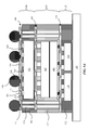
- FIG. 9B is a cross-sectional side view illustration of a three layer stack structure prior to singulation of individual packages in accordance with an embodiment.
- FIG. 10 is a cross-sectional side view illustration of a vertically stacked SiP structure in accordance with an embodiment.
- FIG. 11 is a cross-sectional side view illustration of a PoP structure in accordance with an embodiment.
- FIG. 12 is a process flow illustrating a method of forming a vertically stacked SiP structure in accordance with an embodiment.
- Embodiments describe vertically stacked SiP structures. In various embodiments, description is made with reference to figures. However, certain embodiments may be practiced without one or more of these specific details, or in combination with other known methods and configurations. In the following description, numerous specific details are set forth, such as specific configurations, dimensions and processes, etc., in order to provide a thorough understanding of the embodiments. In other instances, well-known semiconductor processes and manufacturing techniques have not been described in particular detail in order to not unnecessarily obscure the embodiments. Reference throughout this specification to “one embodiment” means that a particular feature, structure, configuration, or characteristic described in connection with the embodiment is included in at least one embodiment. Thus, the appearances of the phrase “in one embodiment” in various places throughout this specification are not necessarily referring to the same embodiment. Furthermore, the particular features, structures, configurations, or characteristics may be combined in any suitable manner in one or more embodiments.
- front”, “back”, “to”, “between”, and “on” as used herein may refer to a relative position of one layer with respect to other layers.
- One layer “on” another layer or bonded “to” or in “contact” with another layer may be directly in contact with the other layer or may have one or more intervening layers.
- One layer “between” layers may be directly in contact with the layers or may have one or more intervening layers.
- a vertical stack SiP includes a first level die encapsulated in a first level molding compound, a first redistribution layer (RDL) on the encapsulated first level die, a second level die stack including a pair of back-to-back stacked die on the first RDL and encapsulated in a second level molding compound, a second RDL on the encapsulated second level die stack, a third level die on the second RDL and encapsulated in a third level molding compound, and a third RDL on the encapsulated third level die.
- RDL redistribution layer
- a plurality of second level conductive pillars may electrically connect the first RDL to the second RDL, and a plurality of third level conductive pillars may electrically connect the second RDL and the third RDL.
- conductive pillars e.g. any of the first level, second level, third level, etc.
- the mechanical support may be provided in addition to electrical connection between components, or without providing electrical connection.
- a portion of the conductive pillars within a package level are to provide electrical connection and mechanical support, while another portion of the conductive pillars within the package level are to provide mechanical support without electrical connection.
- a vertical stack SiP that integrates multiple types of memory die with a logic die (e.g. ASIC or SoC).
- a vertical stack SiP includes separate molding levels for a volatile memory (e.g. DRAM, SRAM, pseudo SRAM, floating body, etc.), non-volatile memory (e.g. NAND, NOR, EPROM, EEPROM, MRAM, FRAM, PCM, etc.), and logic die.
- a vertical stack SiP includes a first level molding including one or more volatile memory die (e.g. DRAM), a second level molding including back-to-back stacked non-volatile memory die (e.g. NAND), and a third level molding including a logic die (e.g ASIC or SoC).
- a vertical stack SiP that may reduce the amount of real estate (e.g. x-y dimensions) on a circuit board. It has been observed that certain non-volatile memory die (e.g. NAND) may have a larger x-y dimension footprint than certain volatile memory die (e.g. DRAM). For example, this may be attributed to an increased memory capacity in mobile devices. In accordance with embodiments, non-volatile memory die for memory may have larger x-y dimensions than volatile memory die (e.g. used for cache). In accordance with embodiments, a vertical stack SiP structure may include multiple first level die arranged side-by-side.
- a vertical stack SiP structure may include multiple second level die with a large x-y dimension (relative to the other die in the SiP) stacked back-to-back within the vertical stack SiP. Additionally, fan out of the back-to-back stacked die can be accomplished with the use of redistribution layers (RDLs) on opposite sides of the back-to-back stacked die. In this manner, the effect on total package height (z-height) can be mitigated with fan out using RDL, which can be fabricated with substantially less thickness than for traditional interposers and wire bonding.
- RDLs redistribution layers
- first level die 110 mounted on a carrier substrate 102 , such as a glass panel, silicon wafer, metal panel, etc.
- the carrier substrate 102 may include an adhesive (e.g. polymer) or tape layer 104 for mounting the plurality of first level die 110 .
- the first level die 110 are mounted onto the carrier substrate with a film 112 such as a die attach film or epoxy bonding material.
- first level die 110 are memory die.
- first level die 110 are volatile memory die such as DRAM, SRAM, pseudo SRAM, floating body, etc.
- first level die 110 are DRAM die.
- first level die 110 are mounted onto the carrier substrate 102 face up, such that the active side including bumps 114 (e.g. stud bumps) is facing up.
- bumps 114 e.g. stud bumps
- stud bumps 114 may be copper stud bumps.
- Bumps 114 may be optional, and instead may be exposed contact pads for the first level die 110 .
- first level conductive pillars 120 may optionally be formed on the carrier substrate 102 .
- the material of optional first level conductive pillars 120 can include, but is not limited to, a metallic material such as copper, titanium, nickel gold, and combinations or alloys thereof.
- First level conductive pillars 120 may be formed using a suitable processing technique, and may be formed of a variety of suitable materials (e.g. copper) and layers. In an embodiment, first level conductive pillars 120 are formed by a plating technique, such as electroplating using a patterned photoresist to define the pillar structure dimensions, followed by removal of the patterned photoresist layer. In an embodiment, the optional first level conductive pillars 120 are formed prior to mounting of the first level die 110 .
- a plating technique such as electroplating using a patterned photoresist to define the pillar structure dimensions, followed by removal of the patterned photoresist layer.
- the optional first level conductive pillars 120 are formed prior to mounting of the first level die 110 .
- the plurality of first level die 110 and optional first level conductive pillars 120 are then encapsulated in a first level molding compound 122 on the carrier substrate 102 .
- the first level molding compound 122 may include a thermosetting cross-linked resin (e.g. epoxy), though other materials may be used as known in electronic packaging. Encapsulation may be accomplished using a suitable technique such as, but not limited to, transfer molding, compression molding, and lamination. Following encapsulation with the first level molding compound 122 , the structure may optionally be additionally processed with a grinding (e.g.
- first level die 110 bumps 114 and optionally first level conductive pillars 120 .
- top surfaces 115 , 123 of the bumps 114 and first level molding compound 122 (and optionally top surfaces 121 of first level conductive pillars 120 ) are coplanar after a grinding or etching operation.
- bumps 114 may be replaced with contact pads of the first level die 110 , which may be exposed, for example, by etching or laser drilling the first level molding compound 122 .
- a first redistribution layer (RDL) 130 is formed on the first level molding compound 122 and the exposed surfaces 115 of bumps 114 (or contact pads), and optionally exposed surfaces 121 of the first level conductive pillars, when present.
- the first RDL 130 may include a single redistribution line 132 or multiple redistribution lines 132 and dielectric layers 134 .
- the first RDL 130 may be formed by a layer-by-layer process, and may be formed using thin film technology.
- the first RDL 130 has a total thickness of less than 50 ⁇ m, or more specifically less than 30 ⁇ m, such as approximately 20 ⁇ m.
- first RDL 130 includes embedded redistribution lines 132 (embedded traces).
- the redistribution lines 132 may be created by first forming a seed layer, followed by forming a metal (e.g. copper) pattern.
- redistribution lines 132 may be formed by deposition (e.g. sputtering) and etching.
- the material of redistribution lines 132 can include, but is not limited to, a metallic material such as copper, titanium, nickel, gold, and combinations or alloys thereof.
- the metal pattern of the redistribution lines 132 is then embedded in a dielectric layer 134 , which is optionally patterned.
- the dielectric layer(s) 134 may be any suitable material such as an oxide, or polymer (e.g. polyimide).
- redistribution lines 132 are formed directly on the top surfaces 115 of bumps 114 (or contact pads). More specifically, contact pads 135 of the redistribution lines 132 of the first RDL 130 are formed directly on the bumps 114 of first level die 110 . Together, the first RDL 130 , and molded first level die 110 may form a first level molding and fan out 135 .
- Second level conductive pillars 140 may be formed similarly, and of the same materials as described above with regard to the optional first level conductive pillars 120 .
- the second level die 142 is a non-volatile memory die, such as (e.g. NAND, NOR, EPROM, EEPROM, MRAM, FRAM, PCM, etc.).
- second level die 142 is a NAND die.
- second level die 142 is wider, with larger x-y area, than either of the first level die 110 . In the embodiment illustrated in FIG.
- second level die 142 is front facing toward the first RDL 130 and is attached to landing pads or underbump metallurgy (UBM) pads of the first RDL 130 with conductive bumps, such as stud bumps, solder bumps, or stud bumps with solder tips.
- conductive bumps such as stud bumps, solder bumps, or stud bumps with solder tips.
- the back side of the second level die 142 does not include any conductive contacts (e.g. stud bumps, solder bumps, etc.).
- FIG. 5B is a close up illustration of a second level die 142 bonded to a first RDL in which landing pad openings have been defined by openings in a dielectric layer 134 .
- the second level die 142 bumps include stud bumps 144 with solder tips 146 .
- FIG. 5C is a close up illustration of a second level die 142 including stud bumps 144 with solder tips 146 bonded to a first RDL in which the landing pads are defined by UBM pads 136 .
- an underfill material 150 may optionally be applied to between the second level die 142 and first RDL 130 .
- a second-second level die 142 is attached to the first-second level die 142 .
- a back side of the second-second level die 142 is attached to a back side of the first-second level die 142 in a back-to-back arrangement.
- the second level die 142 may be attached to each other using a die attach film (DAF) 148 , for example.
- DAF 148 may be an adhesive material, and may optionally be thermally conductive. DAF may optionally be cured after die attachment through chemical, thermal or ultraviolet light, for example.
- the first (e.g. top in FIG. 6 ) and second (e.g. bottom in FIG. 6 ) second level die 142 are identical.
- each second level die 142 may be the same NAND die.
- the stacked second level die 142 are the same, with one exception being a modification to the stud bumps.
- the top second level die 142 (as shown in FIG. 6 ) may include stud bumps 144 without solder tips (or alternatively contact pads where stud bumps are not present), while the bottom second level die 142 (as shown in FIG. 6 ) includes stud bumps 144 with solder tips 146 , as illustrated in FIGS. 5B-5C .
- second level die 142 stack and second level conductive pillars 140 are encapsulated in a second level molding compound 152 on the carrier substrate 102 .
- the second level molding compound 152 may optionally surround the first level molding compound 122 , though this is not required.
- the second level molding compound 152 may be formed similarly as, and from the same material as the first level molding compound 122 .
- the structure may optionally be processed with a grinding operation, etching operation, or patterned and etched to expose the top second level die 142 bumps 144 (or contact pads if bumps are not present), and second level conductive pillars 140 .
- the top surfaces 145 of the bumps 144 , the top surface 153 of the second level molding compound 152 , and the top surfaces 141 of the second level conductive pillars 140 are coplanar after a grinding or etching operation.
- a second redistribution layer (RDL) 160 is then formed on the second level molding compound 152 , the exposed surfaces 145 of bumps 144 (or contact pads), and the exposed surfaces 141 of the second level conductive pillars 140 .
- the second RDL 160 may include a single redistribution line 162 or multiple redistribution lines 162 and dielectric layers 164 .
- the second RDL 160 may be formed by a layer-by-layer process, and may be formed using thin film technology.
- the second RDL 160 has a total thickness of less than 50 ⁇ m, or more specifically less than 30 ⁇ m, such as approximately 20 ⁇ m.
- second RDL 160 includes embedded redistribution lines 162 (embedded traces).
- the redistribution lines 162 may be created by first forming a seed layer, followed by forming a metal (e.g. copper) pattern.
- redistribution lines 162 may be formed by deposition (e.g. sputtering) and etching.
- the material of redistribution lines 162 can include, but is not limited to, a metallic material such as copper, titanium, nickel, gold, and combinations or alloys thereof.
- the metal pattern of the redistribution lines 162 is then embedded in a dielectric layer 164 , which is optionally patterned.
- the dielectric layer(s) 164 may be any suitable material such as an oxide, or polymer (e.g. polyimide).
- redistribution lines 162 are formed directly on the top surfaces 145 of bumps 144 (or contact pads where bumps are not present). More specifically, contact pads 165 of the redistribution lines 162 of the second RDL 160 are formed directly on the bumps 144 of the top second level die 142 . Together, the second RDL 160 , and molded second level stacked die 142 may form a second level molding and fan out 155 . Redistribution lines 162 may also be formed directly on the surfaces 141 of the plurality of second level conductive pillars 140 .
- third level conductive pillars 170 may be formed on the second RDL 160 as illustrated in FIG. 8 .
- Third level conductive pillars may be formed similarly, and of the same materials as described above with regard to the optional first level conductive pillars 120 .
- one or more third level die 172 are mounted on the second RDL 160 .
- the one or more third level die 172 may be mounted after the formation of third level conductive pillars 170 .
- the third level die 172 is a logic die, such as an ASIC or SoC.
- third level die 172 is an SoC die.
- third level die 172 may be back facing to the second RDL 160 .
- the third level die 172 may be attached to the second RDL 160 with a DAF 178 , similar to DAF 148 described above.
- Third level die 172 may include bumps 174 , such as stud bumps (e.g. copper stud bumps).
- third level die 172 may include exposed contact pads in place of bumps 174 .
- third level die 172 and third level conductive pillars 170 are encapsulated in a third level molding compound 182 on the carrier substrate 102 .
- the third level molding compound 182 may optionally surround the first and second level molding compounds 122 , 152 , though this is not required.
- the third level molding compound 182 may be formed similarly as, and from the same material as the first and second level molding compounds 122 , 152 .
- the structure may optionally be processed with a grinding operation, etching operation, or patterned and etched to expose the third level die 172 bumps 174 , (or contact pads) and third level conductive pillars 170 .
- the top surfaces 175 of the bumps 174 , the top surface 183 of the third level molding compound 182 , and the top surfaces 171 of the third level conductive pillars 170 are coplanar after a grinding or etching operation.
- a third redistribution layer (RDL) 190 is then formed on the third level molding compound 182 , the exposed surfaces 175 of bumps 174 (or contact pads), and the exposed surfaces 171 of the third level conductive pillars 170 .
- the third RDL 190 may include a single redistribution line 192 or multiple redistribution lines 192 and dielectric layers 194 .
- the third RDL 190 may be formed by a layer-by-layer process, and may be formed using thin film technology.
- the third RDL 190 has a total thickness of less than 50 ⁇ m, or more specifically less than 30 ⁇ m, such as approximately 20 ⁇ m.
- third RDL 190 includes embedded redistribution lines 192 (embedded traces).
- the redistribution lines 192 may be created by first forming a seed layer, followed by forming a metal (e.g. copper) pattern.
- redistribution lines 192 may be formed by deposition (e.g. sputtering) and etching.
- the material of redistribution lines 192 can include, but is not limited to, a metallic material such as copper, titanium, nickel, gold, and combinations or alloys thereof.
- the metal pattern of the redistribution lines 192 is then embedded in a dielectric layer 194 , which is optionally patterned.
- the dielectric layer(s) 194 may be any suitable material such as an oxide, or polymer (e.g. polyimide).
- redistribution lines 192 are formed directly on the top surfaces 175 of bumps 174 . More specifically, contact pads 195 of the redistribution lines 192 of the third RDL 190 are formed directly on the bumps 174 (or contact pads) of die 172 . Together, the third RDL 190 , and molded third level die 172 may form a third level molding and fan out 185 . Following the formation of the third RDL 190 a plurality of conductive bumps 198 (e.g. solder bumps, or stud bumps) may be formed on the third RDL 190 .
- conductive bumps 198 e.g. solder bumps, or stud bumps
- edges of the molding compounds 122 , 152 may be notched to accommodate a molding cavity for use during encapsulation.
- the notched area may sequentially be trimmed during singulation.
- the particular embodiment illustrated in FIG. 9B is exemplary, and a variety of molding configurations are possible.
- the same or different molding cavities may be used for the different molding levels. Additionally, the molding cavities can have the same or different depths (height), and area. In an embodiment, same molding cavity can be used for all molding levels.
- FIG. 10 is a cross-sectional side view illustration of a vertically stacked SiP structure after removal of the carrier substrate and package singulation.
- a vertically stacked SiP includes a first level die 110 encapsulated in a first level molding compound 122 , a first redistribution layer (RDL) 130 on the encapsulated first level die 110 , a second level die stack including a pair of back-to-back stacked die 142 on the first RDL 130 and encapsulated in a second level molding compound 152 , a second RDL 160 on the encapsulated second level die stack, a third level die 172 on the second RDL 160 and encapsulated in a third level molding compound 182 , and a third RDL 190 on the encapsulated third level die 172 .
- RDL redistribution layer
- a plurality of second level conductive pillars 140 may electrically connect the first RDL 130 to the second RDL 160
- a plurality of third level conductive pillars 170 may electrically connect the second RDL 160 and the third RDL 190
- the third level die 172 is back facing toward the second RDL 160 (e.g. there are no conductive contacts on the back side of the third level die 172 facing the second RDL 160 ). In such a configuration, there is no direct electrical connection between the third level die 172 and the second RDL 160 .
- the third level die 172 may be attached to the second RDL with a die attach film 178 .
- the third RDL 190 may be directly on a conductive bump 174 (e.g. stud bump) of the third level die 172 .
- an electrical path between the third level die 172 and the second RDL 160 runs through the third RDL 190 and third level conductive pillars 170 to the second RDL 160 .
- the first level die 110 is front facing toward the first RDL.
- the first RDL 130 may be directly on a conductive bump 114 (e.g. stud bump) of the first level die 110 .
- the one or more first level die 110 are DRAM die.
- the pair of back-to-back stacked die 142 may include a first-second level die 142 bonded to the first RDL 130 , and a second-second level die 142 , where the second RDL 160 is on the second-second level die 142 .
- the first-second level die 142 may be bonded to the first RDL 130 with solder.
- the second RDL 160 may be directly on a conductive bump 144 (e.g. stud bump) of the second-second level die 142 .
- the second-second level die 142 may be attached to the first-second level die 142 with a die attach film 148 .
- the pair of back-to-back stacked die 142 are non-volatile memory die, such as NAND die.
- the NAND die are stacked back-to-back, as opposed to side-by-side due to their comparatively large size.
- total package size, both x-y and z-height may be reduced using the back-to-back stacking configuration within the middle of the package.
- a plurality of second level conductive pillars 140 may extend from the first RDL 130 to the second RDL 160 , and be encapsulated within the second level molding compound 152 .
- a plurality of third level conductive pillars 170 may extend from the second RDL 160 to the third RDL 190 , and be encapsulated within the third level molding compound 182 .
- a plurality of conductive bumps 198 may be formed on an opposite side of the third RDL 190 from the third level die 172 .
- the third level die 172 is attached to the second RDL 160 with a die attach film 178 .
- the one or more first level die 110 is a volatile memory die (e.g. DRAM)
- the pair of back-to-back stacked die 142 are non-volatile memory die (e.g. NAND)
- the third level die is a logic die (e.g. SoC).
- a passivation layer 200 is optionally formed over the first level molding compound 122 and first level die 110 .
- passivation layer 200 may be formed by lamination.
- the passivation layer 200 is formed after removal of the carrier substrate 102 and prior to singulation of the SiP structures.
- the passivation layer 200 can be formed on the carrier substrate 102 illustrated in FIG. 1 prior to formation of the optional first level conductive pillars 120 and/or attachment of the first level die 110 .
- passivation layer 200 can be formed over the adhesive (e.g. polymer) or tape layer 104 .
- FIG. 11 is a cross-sectional side view illustration of a PoP structure in accordance with an embodiment.
- first level conductive pillars 120 are optionally formed on the carrier substrate 102 , and encapsulated with a first level molding compound 122 .
- the first level conductive pillars 120 may be exposed. Additional processing such as grinding or etching may also be performed to expose the first level conductive pillars.
- a second package 210 may be in electrical connection (e.g. bonded to with conductive bumps 198 ) the first level conductive pillars 120 extending through the first level molding compound 122 of the vertically stacked SiP structure to form a PoP structure.
- FIG. 12 is a process flow illustrating a method of forming a vertically stacked system in package in accordance with an embodiment.
- a first level die is encapsulated on a carrier substrate with a first level molding compound, for example, similarly as described with regard to FIG. 2 .
- a first RDL is formed on the first level molding compound, for example, similarly as described with regard to FIG. 3 .
- the first RDL is formed directly on the first level die.
- a second level die stack is encapsulated on the first RDL with a second level molding compound, for example, similarly as described with regard to FIGS. 4-6 .
- the second level die stack is formed by bonding a first-second level die to the first RDL, and attaching a second-second level die to the first-second level die with a die attach film.
- a plurality of second level conductive pillars formed on the first RDL are encapsulated with the second level molding compound.
- a second RDL is formed on the second level molding compound, for example, similarly as described with regard to FIG. 6 .
- the second RDL is formed directly on the second-second level die in the second level die stack and the plurality of second level conductive pillars.
- a third level die is encapsulated on the second RDL with a third level molding compound, for example, similarly as described with regard to FIG.
- a plurality of third level conductive pillars formed on the second RDL are encapsulated with the third level molding compound.
- a third RDL is formed on the third level molding compound.
- the third RDL may be formed directly on the third level die and the plurality of third level conductive pillars.
- a plurality of conductive bumps e.g. solder balls
- the carrier substrate may then be released.
- this may result in a vertically stacked SiP structure similar to that described with regard to FIG. 10 .
- a second package can be stacked on the vertically stacked SiP structure to form a PoP structure, similar to that described with regard to FIG. 11 .
Landscapes
- Engineering & Computer Science (AREA)
- Manufacturing & Machinery (AREA)
- Production Of Multi-Layered Print Wiring Board (AREA)
- Structures Or Materials For Encapsulating Or Coating Semiconductor Devices Or Solid State Devices (AREA)
- Semiconductor Memories (AREA)
Abstract
Description
Claims (16)
Priority Applications (7)
| Application Number | Priority Date | Filing Date | Title |
|---|---|---|---|
| US14/804,261 US9601471B2 (en) | 2015-04-23 | 2015-07-20 | Three layer stack structure |
| KR1020177033472A KR101939015B1 (en) | 2015-04-23 | 2016-03-08 | A package that is a vertical stacking system including a first level die, a stack of back level second level dies, and a third level die having corresponding first, second and third rewiring layers and a method of making the same |
| JP2017555328A JP6621843B2 (en) | 2015-04-23 | 2016-03-08 | A vertical stack comprising a first level die, a second level die stacked back to back, and a third level die and having corresponding first, second, and third redistribution layers System in package and manufacturing method thereof |
| PCT/US2016/021405 WO2016171805A1 (en) | 2015-04-23 | 2016-03-08 | Vertical stack system in package comprising a first level die, back-to-back stacked second level dies and a third level die with corresponding first, second and third redistribution layers and method of manufacturing thereof |
| CN201680023338.6A CN107533985B (en) | 2015-04-23 | 2016-03-08 | Vertically stacked system-in-package and method of making the same |
| TW105108870A TWI594396B (en) | 2015-04-23 | 2016-03-22 | Vertical stacking of system-level packages and methods of forming a vertically stacked system-in-package |
| US15/405,046 US9935087B2 (en) | 2015-04-23 | 2017-01-12 | Three layer stack structure |
Applications Claiming Priority (2)
| Application Number | Priority Date | Filing Date | Title |
|---|---|---|---|
| US201562151843P | 2015-04-23 | 2015-04-23 | |
| US14/804,261 US9601471B2 (en) | 2015-04-23 | 2015-07-20 | Three layer stack structure |
Related Child Applications (1)
| Application Number | Title | Priority Date | Filing Date |
|---|---|---|---|
| US15/405,046 Continuation US9935087B2 (en) | 2015-04-23 | 2017-01-12 | Three layer stack structure |
Publications (2)
| Publication Number | Publication Date |
|---|---|
| US20160315071A1 US20160315071A1 (en) | 2016-10-27 |
| US9601471B2 true US9601471B2 (en) | 2017-03-21 |
Family
ID=55543133
Family Applications (2)
| Application Number | Title | Priority Date | Filing Date |
|---|---|---|---|
| US14/804,261 Active US9601471B2 (en) | 2015-04-23 | 2015-07-20 | Three layer stack structure |
| US15/405,046 Active US9935087B2 (en) | 2015-04-23 | 2017-01-12 | Three layer stack structure |
Family Applications After (1)
| Application Number | Title | Priority Date | Filing Date |
|---|---|---|---|
| US15/405,046 Active US9935087B2 (en) | 2015-04-23 | 2017-01-12 | Three layer stack structure |
Country Status (6)
| Country | Link |
|---|---|
| US (2) | US9601471B2 (en) |
| JP (1) | JP6621843B2 (en) |
| KR (1) | KR101939015B1 (en) |
| CN (1) | CN107533985B (en) |
| TW (1) | TWI594396B (en) |
| WO (1) | WO2016171805A1 (en) |
Cited By (30)
| Publication number | Priority date | Publication date | Assignee | Title |
|---|---|---|---|---|
| EP2330125A2 (en) | 2005-08-11 | 2011-06-08 | Amylin Pharmaceuticals, Inc. | Hybrid polypeptides with selectable properties |
| EP2330124A2 (en) | 2005-08-11 | 2011-06-08 | Amylin Pharmaceuticals Inc. | Hybrid polypeptides with selectable properties |
| EP2417980A1 (en) | 2004-02-11 | 2012-02-15 | Amylin Pharmaceuticals Inc. | Hybrid polypeptides with selectable properties |
| US20150282367A1 (en) * | 2014-03-27 | 2015-10-01 | Hans-Joachim Barth | Electronic assembly that includes stacked electronic components |
| US20170141088A1 (en) * | 2015-04-23 | 2017-05-18 | Apple Inc. | Three layer stack structure |
| EP3406347A2 (en) | 2012-02-27 | 2018-11-28 | Amunix Operating Inc. | Xten conjugate compositions and methods of making same |
| EP3581579A1 (en) | 2009-02-03 | 2019-12-18 | Amunix Pharmaceuticals, Inc. | Extended recombinant polypeptides and compositions comprising same |
| US10985138B2 (en) | 2017-06-07 | 2021-04-20 | Samsung Electronics Co., Ltd. | Semiconductor package having a plurality of chips and method of manufacturing the same |
| WO2021097186A1 (en) | 2019-11-13 | 2021-05-20 | Amunix Pharmaceuticals, Inc. | Barcoded xten polypeptides and compositions thereof, and methods for making and using the same |
| EP4082541A1 (en) | 2012-09-27 | 2022-11-02 | The Children's Medical Center Corporation | Compounds for the treatment of obesity and methods of use thereof |
| US20240006396A1 (en) * | 2022-07-01 | 2024-01-04 | Advanced Semiconductor Engineering, Inc. | Optical device |
| US11901336B2 (en) | 2020-10-29 | 2024-02-13 | Samsung Electronics Co., Ltd. | Semiconductor package |
| US20240178114A1 (en) * | 2022-11-28 | 2024-05-30 | Samsung Electronics Co., Ltd. | Semiconductor package and method of fabricating the same |
| US12040313B2 (en) | 2019-07-25 | 2024-07-16 | Samsung Electronics Co., Ltd. | Semiconductor package and a method for manufacturing the same |
| US20240241329A1 (en) * | 2021-03-03 | 2024-07-18 | Taiwan Semiconductor Manufacturing Co., Ltd. | Heterogeneous packaging integration of photonic and electronic elements |
| US20240332152A1 (en) * | 2023-04-03 | 2024-10-03 | Yangtze Memory Technologies Co., Ltd. | Integrated package device, fabrication method thereof and memory system |
| US12125775B2 (en) | 2020-11-11 | 2024-10-22 | Nepes Co., Ltd. | Semiconductor package and method for manufacturing the same |
| US12153865B2 (en) | 2016-12-14 | 2024-11-26 | iCometrue Company Ltd. | Logic drive based on standard commodity FPGA IC chips |
| US12176278B2 (en) | 2021-05-30 | 2024-12-24 | iCometrue Company Ltd. | 3D chip package based on vertical-through-via connector |
| US12176902B2 (en) | 2017-09-12 | 2024-12-24 | iCometrue Company Ltd. | Logic drive with brain-like elasticity and integrality based on standard commodity FPGA IC chips using non-volatile memory cells |
| US12183704B2 (en) | 2020-11-11 | 2024-12-31 | Nepes Co., Ltd. | Semiconductor package and method for manufacturing the same |
| US12255195B2 (en) | 2017-08-08 | 2025-03-18 | iCometrue Company Ltd. | Logic drive based on standardized commodity programmable logic semiconductor IC chips |
| US12327816B2 (en) | 2018-11-02 | 2025-06-10 | iCometrue Company Ltd. | Logic drive based on chip scale package comprising standardized commodity programmable logic IC chip and memory IC chip |
| US12327790B2 (en) | 2019-08-05 | 2025-06-10 | iCometrue Company Ltd. | Vertical interconnect elevator based on through silicon vias |
| US12327813B2 (en) | 2018-10-04 | 2025-06-10 | iCometrue Company | Logic drive based on multichip package using interconnection bridge |
| US12368438B2 (en) | 2017-07-11 | 2025-07-22 | iCometrue Company Ltd. | Logic drive based on standard commodity FPGA IC chips using non-volatile memory cells |
| US12464820B2 (en) | 2018-09-11 | 2025-11-04 | iCometrue Company Ltd. | Logic drive using standard commodity programmable logic IC chips comprising non-volatile random access memory cells |
| US12476637B2 (en) | 2018-05-24 | 2025-11-18 | iCometrue Company Ltd. | Logic drive using standard commodity programmable logic IC chips |
| US12519033B2 (en) | 2021-01-08 | 2026-01-06 | iCometrue Company Ltd. | Micro heat pipe for use in semiconductor IC chip package |
| US12555628B2 (en) | 2021-09-24 | 2026-02-17 | iCometrue Company Ltd. | Multi-output look-up table (LUT) for use in coarse-grained field-programmable-gate-array (FPGA) integrated-circuit (IC) chip |
Families Citing this family (111)
| Publication number | Priority date | Publication date | Assignee | Title |
|---|---|---|---|---|
| US9768145B2 (en) | 2015-08-31 | 2017-09-19 | Taiwan Semiconductor Manufacturing Company, Ltd. | Methods of forming multi-die package structures including redistribution layers |
| CN108292653B (en) | 2015-09-25 | 2022-11-08 | 英特尔公司 | Method, apparatus and system for interconnecting packaged integrated circuit dies |
| US20170098629A1 (en) * | 2015-10-05 | 2017-04-06 | Mediatek Inc. | Stacked fan-out package structure |
| US9984998B2 (en) * | 2016-01-06 | 2018-05-29 | Taiwan Semiconductor Manufacturing Company, Ltd. | Devices employing thermal and mechanical enhanced layers and methods of forming same |
| CN105514071B (en) * | 2016-01-22 | 2019-01-25 | 中芯长电半导体(江阴)有限公司 | A fan-out chip packaging method and packaging structure |
| US10204893B2 (en) | 2016-05-19 | 2019-02-12 | Invensas Bonding Technologies, Inc. | Stacked dies and methods for forming bonded structures |
| US9818729B1 (en) * | 2016-06-16 | 2017-11-14 | Taiwan Semiconductor Manufacturing Company, Ltd. | Package-on-package structure and method |
| US9859253B1 (en) * | 2016-06-29 | 2018-01-02 | Intel Corporation | Integrated circuit package stack |
| US11469215B2 (en) * | 2016-07-13 | 2022-10-11 | Taiwan Semiconductor Manufacturing Co., Ltd. | Chip package structure with molding layer and method for forming the same |
| US9825007B1 (en) * | 2016-07-13 | 2017-11-21 | Taiwan Semiconductor Manufacturing Co., Ltd. | Chip package structure with molding layer and method for forming the same |
| US10276548B2 (en) * | 2016-09-14 | 2019-04-30 | Taiwan Semiconductor Manufacturing Company, Ltd. | Semiconductor packages having dummy connectors and methods of forming same |
| US9859245B1 (en) * | 2016-09-19 | 2018-01-02 | Taiwan Semiconductor Manufacturing Co., Ltd. | Chip package structure with bump and method for forming the same |
| US10319698B2 (en) | 2016-11-17 | 2019-06-11 | Intel Corporation | Microelectronic device package having alternately stacked die |
| US10622340B2 (en) * | 2016-11-21 | 2020-04-14 | Samsung Electronics Co., Ltd. | Semiconductor package |
| US10373931B2 (en) * | 2016-11-29 | 2019-08-06 | Taiwan Semiconductor Manufacturing Company Ltd. | Semiconductor package structure and method of manufacturing the same |
| WO2018111249A1 (en) * | 2016-12-14 | 2018-06-21 | Intel Corporation | Integrated circuit packages with plates |
| CN106653709A (en) * | 2016-12-30 | 2017-05-10 | 三星半导体(中国)研究开发有限公司 | Package and manufacturing thereof |
| US10181455B2 (en) | 2017-01-17 | 2019-01-15 | Apple Inc. | 3D thin profile pre-stacking architecture using reconstitution method |
| US10319683B2 (en) * | 2017-02-08 | 2019-06-11 | Taiwan Semiconductor Manufacturing Company, Ltd. | Multi-stacked package-on-package structures |
| US10529698B2 (en) | 2017-03-15 | 2020-01-07 | Taiwan Semiconductor Manufacturing Company, Ltd. | Semiconductor packages and methods of forming same |
| TWI638439B (en) * | 2017-04-17 | 2018-10-11 | Powertech Technology Inc. | Semiconductor package structure and method of manufacturing same |
| KR102275684B1 (en) | 2017-04-18 | 2021-07-13 | 삼성전자주식회사 | Semiconductor package |
| US10943869B2 (en) | 2017-06-09 | 2021-03-09 | Apple Inc. | High density interconnection using fanout interposer chiplet |
| WO2018225589A1 (en) * | 2017-06-09 | 2018-12-13 | 株式会社村田製作所 | Electronic component module |
| CN109103167B (en) * | 2017-06-20 | 2020-11-03 | 晟碟半导体(上海)有限公司 | Heterogeneous fan out structure for memory devices |
| US10283474B2 (en) | 2017-06-30 | 2019-05-07 | Taiwan Semiconductor Manufacturing Co., Ltd. | Chip package structure and method for forming the same |
| TWI633635B (en) * | 2017-07-10 | 2018-08-21 | 台星科股份有限公司 | Stacked chip packaging structure capable of improving space utilization rate and packaging method thereof |
| TWI622143B (en) * | 2017-07-27 | 2018-04-21 | Siliconware Precision Industries Co., Ltd. | Electronic package and its manufacturing method |
| US10510721B2 (en) * | 2017-08-11 | 2019-12-17 | Advanced Micro Devices, Inc. | Molded chip combination |
| US10475747B2 (en) * | 2017-08-14 | 2019-11-12 | Taiwan Semiconductor Manufacturing Co., Ltd. | Integrated fan-out package and method for fabricating the same |
| US20190067145A1 (en) * | 2017-08-22 | 2019-02-28 | Micron Technology, Inc. | Semiconductor device |
| JP6892360B2 (en) * | 2017-09-19 | 2021-06-23 | キオクシア株式会社 | Semiconductor device |
| US11296052B2 (en) * | 2017-09-30 | 2022-04-05 | Intel Corporation | TSV-less die stacking using plated pillars/through mold interconnect |
| US10763239B2 (en) * | 2017-10-27 | 2020-09-01 | Taiwan Semiconductor Manufacturing Co., Ltd. | Multi-chip wafer level packages and methods of forming the same |
| US10957672B2 (en) * | 2017-11-13 | 2021-03-23 | Taiwan Semiconductor Manufacturing Company, Ltd. | Package structure and method of manufacturing the same |
| US10651126B2 (en) * | 2017-12-08 | 2020-05-12 | Applied Materials, Inc. | Methods and apparatus for wafer-level die bridge |
| KR102455427B1 (en) * | 2017-12-20 | 2022-10-17 | 삼성전자주식회사 | Semiconductor package and manufacturing method thereof |
| EP3732717A4 (en) | 2017-12-29 | 2021-09-01 | Intel Corporation | MICROELECTRONIC UNITS EQUIPPED WITH COMMUNICATION NETWORKS |
| DE112017008327T5 (en) | 2017-12-29 | 2020-10-08 | Intel Corporation | MICROELECTRONIC ARRANGEMENTS |
| WO2019132971A1 (en) | 2017-12-29 | 2019-07-04 | Intel Corporation | Microelectronic assemblies |
| WO2019132963A1 (en) | 2017-12-29 | 2019-07-04 | Intel Corporation | Quantum computing assemblies |
| DE112017008336T5 (en) | 2017-12-29 | 2020-09-17 | Intel Corporation | Microelectronic assemblies |
| US10475767B2 (en) * | 2018-01-04 | 2019-11-12 | Kabushiki Kaisha Toshiba | Electronic device |
| WO2019139625A1 (en) * | 2018-01-12 | 2019-07-18 | Intel Corporation | First layer interconnect first on carrier approach for emib patch |
| US11315891B2 (en) | 2018-03-23 | 2022-04-26 | Taiwan Semiconductor Manufacturing Company, Ltd. | Methods of forming semiconductor packages having a die with an encapsulant |
| US10356903B1 (en) * | 2018-03-28 | 2019-07-16 | Apple Inc. | System-in-package including opposing circuit boards |
| US11735570B2 (en) * | 2018-04-04 | 2023-08-22 | Intel Corporation | Fan out packaging pop mechanical attach method |
| US10742217B2 (en) | 2018-04-12 | 2020-08-11 | Apple Inc. | Systems and methods for implementing a scalable system |
| US11276676B2 (en) | 2018-05-15 | 2022-03-15 | Invensas Bonding Technologies, Inc. | Stacked devices and methods of fabrication |
| US10608638B2 (en) * | 2018-05-24 | 2020-03-31 | iCometrue Company Ltd. | Logic drive using standard commodity programmable logic IC chips |
| KR102448248B1 (en) * | 2018-05-24 | 2022-09-27 | 삼성전자주식회사 | Package-on-package type semiconductor package and method for fabricating the same |
| US10658287B2 (en) * | 2018-05-30 | 2020-05-19 | Taiwan Semiconductor Manufacturing Co., Ltd. | Semiconductor device having a tapered protruding pillar portion |
| US10601965B2 (en) * | 2018-06-03 | 2020-03-24 | World Richman Manufacturing Corporation | Cradle assembly and formation for a mobile communications device |
| US11469206B2 (en) | 2018-06-14 | 2022-10-11 | Intel Corporation | Microelectronic assemblies |
| US10854552B2 (en) * | 2018-06-29 | 2020-12-01 | Taiwan Semiconductor Manufacturing Company, Ltd. | Semiconductor device and method of manufacture |
| US10930633B2 (en) * | 2018-06-29 | 2021-02-23 | Taiwan Semiconductor Manufacturing Company, Ltd. | Buffer design for package integration |
| US11158606B2 (en) | 2018-07-06 | 2021-10-26 | Invensas Bonding Technologies, Inc. | Molded direct bonded and interconnected stack |
| WO2020010265A1 (en) | 2018-07-06 | 2020-01-09 | Invensas Bonding Technologies, Inc. | Microelectronic assemblies |
| US10950554B2 (en) * | 2018-07-16 | 2021-03-16 | Taiwan Semiconductor Manufacturing Company, Ltd. | Semiconductor packages with electromagnetic interference shielding layer and methods of forming the same |
| CN108831861A (en) * | 2018-08-09 | 2018-11-16 | 苏州晶方半导体科技股份有限公司 | Stacked chip packages method and encapsulating structure |
| KR102536269B1 (en) * | 2018-09-14 | 2023-05-25 | 삼성전자주식회사 | semiconductor package and method for manufacturing the same |
| CN113330557A (en) | 2019-01-14 | 2021-08-31 | 伊文萨思粘合技术公司 | Bonding structure |
| US10770433B1 (en) * | 2019-02-27 | 2020-09-08 | Apple Inc. | High bandwidth die to die interconnect with package area reduction |
| US12183675B2 (en) | 2019-03-13 | 2024-12-31 | Advanced Micro Devices, Inc. | Fan-out packages with warpage resistance |
| US11239173B2 (en) * | 2019-03-28 | 2022-02-01 | Taiwan Semiconductor Manufacturing Co., Ltd. | Structure and formation method of chip package with fan-out feature |
| KR20250099267A (en) | 2019-04-15 | 2025-07-01 | 양쯔 메모리 테크놀로지스 씨오., 엘티디. | Bonded semiconductor devices having processor and dynamic random-access memory and methods for forming the same |
| EP3891784B1 (en) * | 2019-04-15 | 2024-12-04 | Yangtze Memory Technologies Co., Ltd. | Integration of three-dimensional nand memory devices with multiple functional chips |
| CN110731012B (en) | 2019-04-15 | 2021-01-29 | 长江存储科技有限责任公司 | Integrated semiconductor device with processor and heterogeneous memory and forming method thereof |
| CN112614831B (en) | 2019-04-15 | 2023-08-08 | 长江存储科技有限责任公司 | Integrated semiconductor device with processor and heterogeneous memory and method of forming the same |
| CN110720143B (en) | 2019-04-30 | 2021-01-29 | 长江存储科技有限责任公司 | Bonded semiconductor device with processor and NAND flash memory and method of forming the same |
| KR102653213B1 (en) | 2019-05-13 | 2024-04-01 | 삼성전기주식회사 | Semiconductor package |
| WO2020240239A1 (en) * | 2019-05-31 | 2020-12-03 | Micron Technology, Inc. | Memory component for a system-on-chip device |
| US11735533B2 (en) * | 2019-06-11 | 2023-08-22 | Intel Corporation | Heterogeneous nested interposer package for IC chips |
| US11056453B2 (en) | 2019-06-18 | 2021-07-06 | Deca Technologies Usa, Inc. | Stackable fully molded semiconductor structure with vertical interconnects |
| US11296053B2 (en) | 2019-06-26 | 2022-04-05 | Invensas Bonding Technologies, Inc. | Direct bonded stack structures for increased reliability and improved yield in microelectronics |
| US11195816B2 (en) * | 2019-07-23 | 2021-12-07 | Taiwan Semiconductor Manufacturing Company, Ltd. | Integrated circuit packages comprising a plurality of redistribution structures and methods of forming the same |
| US11094635B2 (en) * | 2019-08-22 | 2021-08-17 | Taiwan Semiconductor Manufacturing Co., Ltd. | Package structure and method for forming the same |
| DE102020106459B4 (en) * | 2019-08-30 | 2023-04-27 | Taiwan Semiconductor Manufacturing Co., Ltd. | CHIP PACKAGE STRUCTURE WITH FORMING LAYER AND METHOD OF FORMING SAME |
| US11856800B2 (en) * | 2019-09-20 | 2023-12-26 | Taiwan Semiconductor Manufacturing Company, Ltd. | Semiconductor devices with system on chip devices |
| DE102020106799A1 (en) | 2019-09-20 | 2021-03-25 | Taiwan Semiconductor Manufacturing Co., Ltd. | SEMICONDUCTOR COMPONENTS AND METHOD OF MANUFACTURING |
| US11158608B2 (en) | 2019-09-25 | 2021-10-26 | Powertech Technology Inc. | Semiconductor package including offset stack of semiconductor dies between first and second redistribution structures, and manufacturing method therefor |
| US11094672B2 (en) * | 2019-09-27 | 2021-08-17 | Intel Corporation | Composite IC chips including a chiplet embedded within metallization layers of a host IC chip |
| KR102741108B1 (en) * | 2019-12-11 | 2024-12-10 | 삼성전자주식회사 | Semiconductor package |
| US11610911B2 (en) * | 2020-01-07 | 2023-03-21 | Micron Technology, Inc. | Semiconductor assemblies including combination memory and methods of manufacturing the same |
| CN111312690A (en) * | 2020-02-14 | 2020-06-19 | 华为技术有限公司 | System-in-package and preparation method thereof |
| KR102765266B1 (en) | 2020-02-25 | 2025-02-07 | 삼성전자주식회사 | Method of manufacturing semiconductor packages |
| KR102752683B1 (en) | 2020-02-28 | 2025-01-10 | 삼성전자주식회사 | Semiconductor package |
| US11264362B2 (en) * | 2020-05-28 | 2022-03-01 | Taiwan Semiconductor Manufacturing Company, Ltd. | Semiconductor structure and method of fabricating the same |
| US11552053B2 (en) | 2020-06-25 | 2023-01-10 | Apple Inc. | Miniaturization of optical sensor modules through wirebonded ball stacks |
| US11631647B2 (en) | 2020-06-30 | 2023-04-18 | Adeia Semiconductor Bonding Technologies Inc. | Integrated device packages with integrated device die and dummy element |
| US11515261B2 (en) * | 2020-09-21 | 2022-11-29 | Apple Inc. | Multiple component integration in fanout package with different back side metallization and thicknesses |
| US11658123B2 (en) * | 2020-09-25 | 2023-05-23 | Advanced Micro Devices, Inc. | Hybrid bridged fanout chiplet connectivity |
| KR102610246B1 (en) * | 2020-11-11 | 2023-12-06 | 주식회사 네패스 | Semiconductor package and method for manufacturing the same |
| US11728266B2 (en) * | 2020-12-23 | 2023-08-15 | Apple Inc. | Die stitching and harvesting of arrayed structures |
| CN112908868A (en) * | 2021-01-18 | 2021-06-04 | 上海先方半导体有限公司 | Three-dimensional packaging method and structure of memory |
| US12125820B2 (en) * | 2021-02-12 | 2024-10-22 | Taiwan Semiconductor Manufacturing Co., Ltd. | Through-dielectric vias for direct connection and method forming same |
| KR102809407B1 (en) | 2021-02-16 | 2025-05-19 | 삼성전자주식회사 | Semiconductor package |
| TWI760227B (en) * | 2021-05-19 | 2022-04-01 | 矽品精密工業股份有限公司 | Electronic package and manufacturing method thereof |
| CN113140550A (en) * | 2021-05-24 | 2021-07-20 | 湖南越摩先进半导体有限公司 | Stacked semiconductor device packaging structure and preparation method thereof |
| US11728248B2 (en) * | 2021-07-01 | 2023-08-15 | Deca Technologies Usa, Inc. | Fully molded semiconductor structure with through silicon via (TSV) vertical interconnects |
| US11616003B2 (en) | 2021-07-01 | 2023-03-28 | Deca Technologies Usa, Inc. | Stackable fully molded semiconductor structure with through silicon via (TSV) vertical interconnects |
| WO2023008111A1 (en) * | 2021-07-26 | 2023-02-02 | 株式会社村田製作所 | Interposer |
| US12165952B2 (en) * | 2022-02-16 | 2024-12-10 | Taiwan Semiconductor Manufacturing Company, Ltd. | Interposer directly bonded to bonding pads on a plurality of dies |
| KR20230143273A (en) * | 2022-04-05 | 2023-10-12 | 삼성전자주식회사 | Semiconductor package |
| KR20240012139A (en) * | 2022-07-20 | 2024-01-29 | 삼성전자주식회사 | Semiconductor chip stack structure, semiconductor package and manufacturing method thereof |
| KR20240023276A (en) * | 2022-08-11 | 2024-02-21 | 삼성전자주식회사 | semiconductor package |
| US20240072029A1 (en) * | 2022-08-23 | 2024-02-29 | Taiwan Semiconductor Manufacturing Company, Ltd. | Semiconductor package and manufacturing method thereof |
| CN118098994A (en) * | 2022-11-21 | 2024-05-28 | 长鑫存储技术有限公司 | Semiconductor structure manufacturing method and semiconductor structure |
| JP7715143B2 (en) * | 2022-12-22 | 2025-07-30 | 株式会社村田製作所 | Composite component device and manufacturing method thereof |
| CN116130458A (en) * | 2023-01-03 | 2023-05-16 | 西安微电子技术研究所 | Prefabricated vertical die through hole die-sealing interconnection substrate structure and manufacturing method |
| WO2025096213A1 (en) * | 2023-10-31 | 2025-05-08 | Micron Technology, Inc. | Stacked semiconductor device with semiconductor dies of variable size |
Citations (10)
| Publication number | Priority date | Publication date | Assignee | Title |
|---|---|---|---|---|
| EP1367645A2 (en) | 2002-05-31 | 2003-12-03 | Fujitsu Limited | Semiconductor device and manufacturing method thereof |
| US20090160053A1 (en) | 2007-12-19 | 2009-06-25 | Infineon Technologies Ag | Method of manufacturing a semiconducotor device |
| KR20100107540A (en) | 2009-03-26 | 2010-10-06 | 대덕전자 주식회사 | Method of fabricating an interconnection structure for multi-functional printed circuit board |
| US20120032340A1 (en) | 2010-08-06 | 2012-02-09 | Stats Chippac, Ltd. | Semiconductor Die and Method of Forming FO-WLCSP Vertical Interconnect Using TSV and TMV |
| US8253244B2 (en) | 2007-08-20 | 2012-08-28 | Samsung Electronics Co., Ltd. | Semiconductor package having memory devices stacked on logic device |
| US8288209B1 (en) | 2011-06-03 | 2012-10-16 | Stats Chippac, Ltd. | Semiconductor device and method of using leadframe bodies to form openings through encapsulant for vertical interconnect of semiconductor die |
| US20130037950A1 (en) * | 2011-08-10 | 2013-02-14 | Taiwan Semiconductor Manufacturing Company, Ltd. | Multi-Chip Wafer Level Package |
| US20130105966A1 (en) | 2011-10-26 | 2013-05-02 | Maxim Integrated Products, Inc. | Three-dimensional chip-to-wafer integration |
| US20130260510A1 (en) | 2012-04-02 | 2013-10-03 | Infineon Technologies Ag | 3-D Integrated Circuits and Methods of Forming Thereof |
| US20160013156A1 (en) * | 2014-07-14 | 2016-01-14 | Apple Inc. | Package-on-package options with multiple layer 3-d stacking |
Family Cites Families (2)
| Publication number | Priority date | Publication date | Assignee | Title |
|---|---|---|---|---|
| US8878360B2 (en) * | 2012-07-13 | 2014-11-04 | Intel Mobile Communications GmbH | Stacked fan-out semiconductor chip |
| US9601471B2 (en) * | 2015-04-23 | 2017-03-21 | Apple Inc. | Three layer stack structure |
-
2015
- 2015-07-20 US US14/804,261 patent/US9601471B2/en active Active
-
2016
- 2016-03-08 JP JP2017555328A patent/JP6621843B2/en active Active
- 2016-03-08 KR KR1020177033472A patent/KR101939015B1/en active Active
- 2016-03-08 WO PCT/US2016/021405 patent/WO2016171805A1/en not_active Ceased
- 2016-03-08 CN CN201680023338.6A patent/CN107533985B/en active Active
- 2016-03-22 TW TW105108870A patent/TWI594396B/en active
-
2017
- 2017-01-12 US US15/405,046 patent/US9935087B2/en active Active
Patent Citations (11)
| Publication number | Priority date | Publication date | Assignee | Title |
|---|---|---|---|---|
| EP1367645A2 (en) | 2002-05-31 | 2003-12-03 | Fujitsu Limited | Semiconductor device and manufacturing method thereof |
| US8253244B2 (en) | 2007-08-20 | 2012-08-28 | Samsung Electronics Co., Ltd. | Semiconductor package having memory devices stacked on logic device |
| US20090160053A1 (en) | 2007-12-19 | 2009-06-25 | Infineon Technologies Ag | Method of manufacturing a semiconducotor device |
| KR20100107540A (en) | 2009-03-26 | 2010-10-06 | 대덕전자 주식회사 | Method of fabricating an interconnection structure for multi-functional printed circuit board |
| US20120032340A1 (en) | 2010-08-06 | 2012-02-09 | Stats Chippac, Ltd. | Semiconductor Die and Method of Forming FO-WLCSP Vertical Interconnect Using TSV and TMV |
| US8288209B1 (en) | 2011-06-03 | 2012-10-16 | Stats Chippac, Ltd. | Semiconductor device and method of using leadframe bodies to form openings through encapsulant for vertical interconnect of semiconductor die |
| US20130037950A1 (en) * | 2011-08-10 | 2013-02-14 | Taiwan Semiconductor Manufacturing Company, Ltd. | Multi-Chip Wafer Level Package |
| US8754514B2 (en) | 2011-08-10 | 2014-06-17 | Taiwan Semiconductor Manufacturing Company, Ltd. | Multi-chip wafer level package |
| US20130105966A1 (en) | 2011-10-26 | 2013-05-02 | Maxim Integrated Products, Inc. | Three-dimensional chip-to-wafer integration |
| US20130260510A1 (en) | 2012-04-02 | 2013-10-03 | Infineon Technologies Ag | 3-D Integrated Circuits and Methods of Forming Thereof |
| US20160013156A1 (en) * | 2014-07-14 | 2016-01-14 | Apple Inc. | Package-on-package options with multiple layer 3-d stacking |
Non-Patent Citations (3)
| Title |
|---|
| English machine translation of KR 2010 0107540 A, Oct. 6, 2010, 14 pages, available online Korean Intellectual Property Office http://www.kipris.or.kr/enghome/main.jsp, n.d. |
| PCT International Search Report and Written Opinion for International Application No. PCT/US2016/021405, mailed Aug. 22, 2016, 20 pages. |
| PCT Invitation to Pay Additional Fees for International Application No. PCT/US2016/021405, mailed May 25, 2016, 8 pages. |
Cited By (34)
| Publication number | Priority date | Publication date | Assignee | Title |
|---|---|---|---|---|
| EP2417980A1 (en) | 2004-02-11 | 2012-02-15 | Amylin Pharmaceuticals Inc. | Hybrid polypeptides with selectable properties |
| EP2422806A2 (en) | 2004-02-11 | 2012-02-29 | Amylin Pharmaceuticals Inc. | Hybrid polypeptides with selectable properties |
| EP2422807A2 (en) | 2004-02-11 | 2012-02-29 | Amylin Pharmaceuticals Inc. | Hybrid polypeptides with selectable properties |
| EP2330124A2 (en) | 2005-08-11 | 2011-06-08 | Amylin Pharmaceuticals Inc. | Hybrid polypeptides with selectable properties |
| EP2330125A2 (en) | 2005-08-11 | 2011-06-08 | Amylin Pharmaceuticals, Inc. | Hybrid polypeptides with selectable properties |
| EP3581579A1 (en) | 2009-02-03 | 2019-12-18 | Amunix Pharmaceuticals, Inc. | Extended recombinant polypeptides and compositions comprising same |
| EP3406347A2 (en) | 2012-02-27 | 2018-11-28 | Amunix Operating Inc. | Xten conjugate compositions and methods of making same |
| EP4082541A1 (en) | 2012-09-27 | 2022-11-02 | The Children's Medical Center Corporation | Compounds for the treatment of obesity and methods of use thereof |
| US20150282367A1 (en) * | 2014-03-27 | 2015-10-01 | Hans-Joachim Barth | Electronic assembly that includes stacked electronic components |
| US20170141088A1 (en) * | 2015-04-23 | 2017-05-18 | Apple Inc. | Three layer stack structure |
| US9935087B2 (en) * | 2015-04-23 | 2018-04-03 | Apple Inc. | Three layer stack structure |
| US12153865B2 (en) | 2016-12-14 | 2024-11-26 | iCometrue Company Ltd. | Logic drive based on standard commodity FPGA IC chips |
| US10985138B2 (en) | 2017-06-07 | 2021-04-20 | Samsung Electronics Co., Ltd. | Semiconductor package having a plurality of chips and method of manufacturing the same |
| US12368438B2 (en) | 2017-07-11 | 2025-07-22 | iCometrue Company Ltd. | Logic drive based on standard commodity FPGA IC chips using non-volatile memory cells |
| US12255195B2 (en) | 2017-08-08 | 2025-03-18 | iCometrue Company Ltd. | Logic drive based on standardized commodity programmable logic semiconductor IC chips |
| US12176902B2 (en) | 2017-09-12 | 2024-12-24 | iCometrue Company Ltd. | Logic drive with brain-like elasticity and integrality based on standard commodity FPGA IC chips using non-volatile memory cells |
| US12476637B2 (en) | 2018-05-24 | 2025-11-18 | iCometrue Company Ltd. | Logic drive using standard commodity programmable logic IC chips |
| US12464820B2 (en) | 2018-09-11 | 2025-11-04 | iCometrue Company Ltd. | Logic drive using standard commodity programmable logic IC chips comprising non-volatile random access memory cells |
| US12327813B2 (en) | 2018-10-04 | 2025-06-10 | iCometrue Company | Logic drive based on multichip package using interconnection bridge |
| US12327816B2 (en) | 2018-11-02 | 2025-06-10 | iCometrue Company Ltd. | Logic drive based on chip scale package comprising standardized commodity programmable logic IC chip and memory IC chip |
| US12040313B2 (en) | 2019-07-25 | 2024-07-16 | Samsung Electronics Co., Ltd. | Semiconductor package and a method for manufacturing the same |
| US12327790B2 (en) | 2019-08-05 | 2025-06-10 | iCometrue Company Ltd. | Vertical interconnect elevator based on through silicon vias |
| WO2021097186A1 (en) | 2019-11-13 | 2021-05-20 | Amunix Pharmaceuticals, Inc. | Barcoded xten polypeptides and compositions thereof, and methods for making and using the same |
| US12237308B2 (en) | 2020-10-29 | 2025-02-25 | Samsung Electronics Co., Ltd. | Semiconductor package |
| US11901336B2 (en) | 2020-10-29 | 2024-02-13 | Samsung Electronics Co., Ltd. | Semiconductor package |
| US12183704B2 (en) | 2020-11-11 | 2024-12-31 | Nepes Co., Ltd. | Semiconductor package and method for manufacturing the same |
| US12125775B2 (en) | 2020-11-11 | 2024-10-22 | Nepes Co., Ltd. | Semiconductor package and method for manufacturing the same |
| US12519033B2 (en) | 2021-01-08 | 2026-01-06 | iCometrue Company Ltd. | Micro heat pipe for use in semiconductor IC chip package |
| US20240241329A1 (en) * | 2021-03-03 | 2024-07-18 | Taiwan Semiconductor Manufacturing Co., Ltd. | Heterogeneous packaging integration of photonic and electronic elements |
| US12176278B2 (en) | 2021-05-30 | 2024-12-24 | iCometrue Company Ltd. | 3D chip package based on vertical-through-via connector |
| US12555628B2 (en) | 2021-09-24 | 2026-02-17 | iCometrue Company Ltd. | Multi-output look-up table (LUT) for use in coarse-grained field-programmable-gate-array (FPGA) integrated-circuit (IC) chip |
| US20240006396A1 (en) * | 2022-07-01 | 2024-01-04 | Advanced Semiconductor Engineering, Inc. | Optical device |
| US20240178114A1 (en) * | 2022-11-28 | 2024-05-30 | Samsung Electronics Co., Ltd. | Semiconductor package and method of fabricating the same |
| US20240332152A1 (en) * | 2023-04-03 | 2024-10-03 | Yangtze Memory Technologies Co., Ltd. | Integrated package device, fabrication method thereof and memory system |
Also Published As
| Publication number | Publication date |
|---|---|
| TWI594396B (en) | 2017-08-01 |
| US20170141088A1 (en) | 2017-05-18 |
| WO2016171805A1 (en) | 2016-10-27 |
| CN107533985B (en) | 2020-08-14 |
| JP6621843B2 (en) | 2019-12-18 |
| TW201709473A (en) | 2017-03-01 |
| JP2018514088A (en) | 2018-05-31 |
| KR20170141733A (en) | 2017-12-26 |
| CN107533985A (en) | 2018-01-02 |
| US20160315071A1 (en) | 2016-10-27 |
| US9935087B2 (en) | 2018-04-03 |
| KR101939015B1 (en) | 2019-01-15 |
Similar Documents
| Publication | Publication Date | Title |
|---|---|---|
| US9935087B2 (en) | Three layer stack structure | |
| TWI627716B (en) | System-in-package fan-out stacking architecture and process flow | |
| KR101949076B1 (en) | Dual-sided mounting memory integrated in a thin, low distortion fan-out package | |
| US11594494B2 (en) | High density interconnection using fanout interposer chiplet | |
| US10181455B2 (en) | 3D thin profile pre-stacking architecture using reconstitution method | |
| US9679801B2 (en) | Dual molded stack TSV package | |
| CN107408547B (en) | Fan-out system-in-package and method of forming the same | |
| CN107851615B (en) | Independent 3D stacking | |
| TW201721771A (en) | Integrated fan-out package and manufacturing method | |
| US11056373B2 (en) | 3D fanout stacking | |
| KR20200035322A (en) | Hybrid add-on stacked memory die using wire bond | |
| US20080237831A1 (en) | Multi-chip semiconductor package structure | |
| US20240315054A1 (en) | Upside-Down DRAM Package Structure | |
| US12456692B2 (en) | Microelectronic package RDL patterns to reduce stress in RDLs across components |
Legal Events
| Date | Code | Title | Description |
|---|---|---|---|
| AS | Assignment |
Owner name: APPLE INC., CALIFORNIA Free format text: ASSIGNMENT OF ASSIGNORS INTEREST;ASSIGNORS:ZHAI, JUN;HU, KUNZHONG;REEL/FRAME:036138/0262 Effective date: 20150714 |
|
| FEPP | Fee payment procedure |
Free format text: PAYOR NUMBER ASSIGNED (ORIGINAL EVENT CODE: ASPN); ENTITY STATUS OF PATENT OWNER: LARGE ENTITY |
|
| STCF | Information on status: patent grant |
Free format text: PATENTED CASE |
|
| MAFP | Maintenance fee payment |
Free format text: PAYMENT OF MAINTENANCE FEE, 4TH YEAR, LARGE ENTITY (ORIGINAL EVENT CODE: M1551); ENTITY STATUS OF PATENT OWNER: LARGE ENTITY Year of fee payment: 4 |
|
| MAFP | Maintenance fee payment |
Free format text: PAYMENT OF MAINTENANCE FEE, 8TH YEAR, LARGE ENTITY (ORIGINAL EVENT CODE: M1552); ENTITY STATUS OF PATENT OWNER: LARGE ENTITY Year of fee payment: 8 |