US9595648B2 - Light-emitting device - Google Patents
Light-emitting device Download PDFInfo
- Publication number
- US9595648B2 US9595648B2 US14/783,239 US201414783239A US9595648B2 US 9595648 B2 US9595648 B2 US 9595648B2 US 201414783239 A US201414783239 A US 201414783239A US 9595648 B2 US9595648 B2 US 9595648B2
- Authority
- US
- United States
- Prior art keywords
- light
- refractive index
- layer
- index layer
- illuminator
- Prior art date
- Legal status (The legal status is an assumption and is not a legal conclusion. Google has not performed a legal analysis and makes no representation as to the accuracy of the status listed.)
- Active
Links
Images


Classifications
-
- H—ELECTRICITY
- H01—ELECTRIC ELEMENTS
- H01L—SEMICONDUCTOR DEVICES NOT COVERED BY CLASS H10
- H01L33/00—Semiconductor devices with at least one potential-jump barrier or surface barrier specially adapted for light emission; Processes or apparatus specially adapted for the manufacture or treatment thereof or of parts thereof; Details thereof
- H01L33/48—Semiconductor devices with at least one potential-jump barrier or surface barrier specially adapted for light emission; Processes or apparatus specially adapted for the manufacture or treatment thereof or of parts thereof; Details thereof characterised by the semiconductor body packages
- H01L33/58—Optical field-shaping elements
-
- G—PHYSICS
- G02—OPTICS
- G02B—OPTICAL ELEMENTS, SYSTEMS OR APPARATUS
- G02B5/00—Optical elements other than lenses
- G02B5/02—Diffusing elements; Afocal elements
- G02B5/0205—Diffusing elements; Afocal elements characterised by the diffusing properties
- G02B5/021—Diffusing elements; Afocal elements characterised by the diffusing properties the diffusion taking place at the element's surface, e.g. by means of surface roughening or microprismatic structures
- G02B5/0221—Diffusing elements; Afocal elements characterised by the diffusing properties the diffusion taking place at the element's surface, e.g. by means of surface roughening or microprismatic structures the surface having an irregular structure
-
- H—ELECTRICITY
- H01—ELECTRIC ELEMENTS
- H01L—SEMICONDUCTOR DEVICES NOT COVERED BY CLASS H10
- H01L33/00—Semiconductor devices with at least one potential-jump barrier or surface barrier specially adapted for light emission; Processes or apparatus specially adapted for the manufacture or treatment thereof or of parts thereof; Details thereof
- H01L33/02—Semiconductor devices with at least one potential-jump barrier or surface barrier specially adapted for light emission; Processes or apparatus specially adapted for the manufacture or treatment thereof or of parts thereof; Details thereof characterised by the semiconductor bodies
- H01L33/20—Semiconductor devices with at least one potential-jump barrier or surface barrier specially adapted for light emission; Processes or apparatus specially adapted for the manufacture or treatment thereof or of parts thereof; Details thereof characterised by the semiconductor bodies with a particular shape, e.g. curved or truncated substrate
- H01L33/22—Roughened surfaces, e.g. at the interface between epitaxial layers
-
- H01L51/5275—
-
- H—ELECTRICITY
- H10—SEMICONDUCTOR DEVICES; ELECTRIC SOLID-STATE DEVICES NOT OTHERWISE PROVIDED FOR
- H10K—ORGANIC ELECTRIC SOLID-STATE DEVICES
- H10K50/00—Organic light-emitting devices
- H10K50/80—Constructional details
- H10K50/85—Arrangements for extracting light from the devices
- H10K50/858—Arrangements for extracting light from the devices comprising refractive means, e.g. lenses
-
- H01L2251/5315—
-
- H01L2251/5369—
-
- H—ELECTRICITY
- H10—SEMICONDUCTOR DEVICES; ELECTRIC SOLID-STATE DEVICES NOT OTHERWISE PROVIDED FOR
- H10K—ORGANIC ELECTRIC SOLID-STATE DEVICES
- H10K2102/00—Constructional details relating to the organic devices covered by this subclass
- H10K2102/301—Details of OLEDs
- H10K2102/302—Details of OLEDs of OLED structures
- H10K2102/3023—Direction of light emission
- H10K2102/3026—Top emission
-
- H—ELECTRICITY
- H10—SEMICONDUCTOR DEVICES; ELECTRIC SOLID-STATE DEVICES NOT OTHERWISE PROVIDED FOR
- H10K—ORGANIC ELECTRIC SOLID-STATE DEVICES
- H10K2102/00—Constructional details relating to the organic devices covered by this subclass
- H10K2102/301—Details of OLEDs
- H10K2102/331—Nanoparticles used in non-emissive layers, e.g. in packaging layer
Definitions
- the present application relates to an illuminator.
- organic electro-luminescence devices those are known in which a hole transport layer, an organic emission layer, an electron transport layer, and a cathode are stacked in this order on a transparent electrode (anode) that is formed on the surface of a transparent substrate.
- anode anode
- light occurs from the organic emission layer.
- the generated light is transmitted through the transparent electrode and the transparent substrate to be extracted to the exterior.
- Organic EL devices are characterized by being self-light-emitting type devices, having emission characteristics with a relatively high efficiency, being capable of emission in various color tones, and so on. Therefore, their application to light-emitting elements in display devices (e.g., flat panel displays) and light sources (e.g., backlights or illuminations for liquid crystal display devices) is considered as promising, and some of that has already matured into practical use. In order to apply organic EL devices to such uses, it is desirable to develop organic EL devices that have good characteristics marked by higher efficiency, longer life, and higher luminance.
- the light extraction efficiency of an organic EL device which is generally on the order of 20% to 30% although subject to some fluctuation depending on the emission pattern and internal layer structure, leaves room for improvement.
- the reason for such low light extraction efficiency is that the material(s) composing the sites of light emission and their neighborhood has characteristics such as a high refractive index and light absorption. This causes a problem in that total reflection may occur at interfaces between different refractive indices and light may be absorbed by the material(s), thus hindering effective light propagation to the exterior where emission is to be observed. Consequently, in an organic EL device, non-available light accounts for 70% to 80% of the total emission amount. Thus, there is a very large expectation of improvements in the efficiency of an organic EL device that are based on light extraction efficiency improvements.
- Patent Document 1 discloses an organic EL device having a diffraction grating for suppressing total reflection at interfaces.
- Patent Document 2 discloses an organic EL device in which a microlens array is provided on the surface of a transparent substrate.
- Patent Document 3 discloses an organic EL device having an optical sheet with an optical layer that includes beads dispersed in a binder.
- Patent Document 1 the specification of Japanese Patent No. 2991183
- Patent Document 2 Japanese Laid-Open Patent Publication No. 2004-241130
- Patent Document 3 Japanese Laid-Open Patent Publication No. 2003-100444
- One non-limiting, and exemplary embodiment of the present application provides an illuminator with an enhanced efficiency of light extraction.
- a light extraction sheet comprises: a light-transmitting substrate having a first principal face and a second principal face; a first light extraction structure on the first principal face side of the light-transmitting substrate, the first light extraction structure including a low-refractive index layer having a lower refractive index than does the light-transmitting substrate and a high-refractive index layer having a higher refractive index than does the low-refractive index layer, the low-refractive index layer being between the light-transmitting substrate and the high-refractive index layer, and an interface between the high-refractive index layer and the low-refractive index layer having bump-dent features; and a second light extraction structure on the second principal face side of the light-transmitting substrate, the second light extraction structure being arranged so that light which is transmitted through the light-transmitting substrate and arrives at an incident angle of 40 degrees to 60 degrees has an average transmittance of 42% or more.
- the aforementioned general/specific implementation can be implemented by using a system, a method, or a computer program, or can be realized by using a combination of a system, a method, and a computer program.
- An illuminator according to an implementation of the present invention provides an enhanced efficiency of light extraction.
- FIG. 1 A cross-sectional view showing an organic EL device according to an illustrative embodiment.
- FIG. 2A A plan view showing an exemplary bump-dent structure.
- FIG. 2B A cross-sectional view showing an exemplary bump-dent structure.
- FIG. 3A A diagram schematically showing an exemplary microlens array.
- FIG. 3B A diagram schematically showing an exemplary light diffusing layer.
- FIG. 4 A diagram showing a measurement method of light transmittance.
- FIG. 5A A plan view showing an exemplary arrangement of a microlens array.
- FIG. 5B A cross-sectional view taken along line A-A′ in FIG. 5A .
- FIG. 6A A diagram showing incident angle dependence of transmittance in the case where a microlens array is used as an external light-extraction layer.
- FIG. 6B A diagram showing incident angle dependence of transmittance in the case where a light diffusing layer is used as an external light-extraction layer.
- FIG. 6C A diagram showing incident angle dependence of transmittance in the case where a light diffusing layer is used as an external light-extraction layer.
- FIG. 7 A diagram showing a method of measuring an angular distribution with which light strikes an external light-extraction layer.
- FIG. 8A A graph showing incident angle dependence of light intensity per unit area in several prototyped devices.
- FIG. 8B A diagram showing the construction of a prototyped device.
- FIG. 9 A diagram showing in (a) and (b) bump-dent structures in prototyped devices.
- FIG. 10 A diagram for explaining Snell's law.
- FIG. 11 A diagram showing incident angle dependence of light intensity where the refractive index of a low-refractive index layer is varied.
- FIG. 12 Experimental results showing how dependence of light extraction efficiency on the refractive index of the low-refractive index layer may differ depending on whether a microlens array is used or a diffusing layer is used.
- FIG. 13 A diagram showing an angular distribution of light from an emission layer, in light extraction efficiency calculation.
- FIG. 14 Calculation results showing how dependence of light extraction efficiency on the refractive index of the low-refractive index layer may differ depending on whether a microlens array is used or a diffusing layer is used.
- FIG. 15 A graph showing dependence of light extraction efficiency on the refractive index of the high-refractive index layer.
- FIG. 16 A graph showing dependence, on the aspect ratio of microlenses, of transmittance of light at an incident angle from 40 to 60 degrees.
- FIG. 17 A graph showing dependence of light intensity on the incident angle, where the aspect ratio is varied.
- FIG. 18 A diagram showing a variant microlens array.
- FIG. 19 A graph showing changes in the incident angle dependence of light intensity under different constructions of the external light-extraction layer.
- FIG. 20A A plan view showing an example where pyramidal structures are adopted for the external light-extraction layer.
- FIG. 20B A cross-sectional view taken along line B-B′ in FIG. 20A .
- FIG. 21 A graph showing dependence of transmittance of light at an incident angle from 40 to 60 degrees on the vertex angle in the case where pyramidal structures are adopted.
- FIG. 22 A graph showing changes in light intensity where the vertex angle of each pyramidal structure is varied.
- FIG. 23 Diagrams (a) and (b) for explaining the period of a bump-dent structure.
- FIG. 24 Another diagram for explaining the period of a bump-dent structure.
- FIG. 25 (a) is a diagram showing a first example of a bump-dent structure; (b) is a diagram showing a second example of a bump-dent structure; and (c) is diagram showing a third example of a bump-dent structure.
- FIG. 26 A graph showing dependence of light extraction efficiency on the width of bump-dent features.
- FIG. 27 Diagrams (a) - (c) showing exemplary bump-dent structures with controlled randomness.
- FIG. 28 A graph showing dependence of light extraction efficiency on the height h of a bump-dent structure, and dependence of light extraction efficiency on the degree of randomness.
- FIG. 29 A graph showing a difference between a completely random pattern and a random pattern with controlled randomness.
- FIG. 30 (a) is a diagram showing Fourier components of a completely random pattern; (b) is a diagram showing Fourier components of a pattern with controlled randomness.
- FIG. 31 A diagram showing a variant bump-dent structure.
- FIG. 32 A diagram showing a measurement method of an angular distribution of emission intensity.
- FIG. 33A A first graph illustrating how the incident angle dependence of light intensity may vary depending on the position of an emission point.
- FIG. 33B A second graph illustrating how the incident angle dependence of light intensity may vary depending on the position of an emission point.
- FIG. 34 A graph showing dependence of emission efficiency on the position of an emission point.
- FIG. 35 A graph showing incident angle dependence of the intensity of light passing through the internal light-extraction layer where the position of the emission point is varied.
- FIG. 36 A graph showing changes in the total amount of light contained in the respective incident angle ranges of 0° to 20° , 20° to 40° , and 40° to 60° where the position of the emission point is varied;
- the inventors have found a novel construction which can reduce the total reflection losses at these two interfaces. Specifically, we have found that the light extraction efficiency can be improved in a construction where: a first light extraction structure to cause light diffraction is provided between an emission layer and a transparent substrate; and a second light extraction structure such as a microlens array is provided on the opposite side of the transparent substrate from the emission layer.
- a first light extraction structure to cause light diffraction is provided between an emission layer and a transparent substrate
- a second light extraction structure such as a microlens array
- An illuminator as one implementation of the present invention comprises: a light-emitting element for emitting light of an average wavelength ⁇ ; and a light extraction sheet which transmits light occurring from the light-emitting element.
- the light-emitting element includes a first electrode having a light transmitting property, a second electrode, and an emission layer between the first and second electrodes.
- the light extraction sheet includes: a light-transmitting substrate having a first principal face and a second principal face; a first light extraction structure on the first principal face side of the light-transmitting substrate, the first light extraction structure including a low-refractive index layer having a lower refractive index than does the light-transmitting substrate and a high-refractive index layer having a higher refractive index than does the low-refractive index layer, the low-refractive index layer being between the light-transmitting substrate and the high-refractive index layer, and an interface between the high-refractive index layer and the low-refractive index layer having bump-dent features; and a second light extraction structure on the second principal face side of the light-transmitting substrate, the second light extraction structure being arranged so that light which is transmitted through the light-transmitting substrate and arrives at an incident angle of 40 degrees to 60 degrees has an average transmittance of 42% or more.
- the bump-dent features comprise a random two-dimensional array of a plurality of dents and a plurality of bumps.
- the bump-dent structure comprises a periodic two-dimensional array of a plurality of dents and a plurality of bumps.
- the bump-dent features comprise a two-dimensional array of a plurality of dents and a plurality of bumps, and among spatial frequency components of a pattern of the bump-dent features, those components which are smaller than 1/(2w) are suppressed as compared to when the plurality of dents and the plurality of bumps are randomly arrayed, where w is a minimum value of lengths of shorter sides of ellipses which are inscribed in the plurality of dents and the plurality of bumps.
- the bump-dent features are arranged so that no predetermined number or more of dents or bumps are successively present along one direction.
- the plurality of dents and the plurality of bumps each have a rectangular cross section, and the bump-dent features are arranged so that no three or more dents or bumps are successively present along one direction.
- the plurality of dents and the plurality of bumps each have a hexagonal cross section, and the bump-dent features are arranged so that no four or more dents or bumps are successively present along one direction.
- a minimum value of lengths of shorter sides of ellipses which are inscribed in the plurality of dents and the plurality of bumps is 0.73 ⁇ or more.
- the plurality of dents and the plurality of bumps have a same cross-sectional shape and a same size.
- the plurality of dents and the plurality of bumps each have an average period of 14.5 ⁇ or less.
- the low-refractive index layer has a refractive index which is 0.98 times or less of a refractive index of the light-transmitting substrate.
- a distance between an emission point in the emission layer and the surface of the second electrode is 0.17 ⁇ or more.
- the low-refractive index layer has a refractive index of 1.47 or less.
- the low-refractive index layer has a thickness of (1 ⁇ 2) ⁇ or more.
- the light-transmitting substrate has a refractive index of 1.5 or more.
- the high-refractive index layer has a refractive index of 1.73 or more.
- the second light extraction structure comprises a microlens array.
- the microlens array has an aspect ratio of 0.5 or more.
- the second light extraction structure comprises pyramidal structures, vertex angles of the pyramidal structures being in a range from 30 degrees to 120 degrees.
- a light extraction sheet as another implementation of the present invention comprises: a light-transmitting substrate having a first principal face and a second principal face; a first light extraction structure on the first principal face side of the light-transmitting substrate, the first light extraction structure including a low-refractive index layer having a lower refractive index than does the light-transmitting substrate and a high-refractive index layer having a higher refractive index than does the low-refractive index layer, the low-refractive index layer being between the light-transmitting substrate and the high-refractive index layer, and an interface between the high-refractive index layer and the low-refractive index layer having bump-dent features; and a second light extraction structure on the second principal face side of the light-transmitting substrate, the second light extraction structure being arranged so that light which is transmitted through the light-transmitting substrate and arrives at an incident angle of 40 degrees to 60 degrees has an average transmittance of 42% or more.
- FIG. 1 is a cross-sectional view showing a schematic construction of an organic EL device 100 according to the present embodiment.
- the organic EL device 100 of the present embodiment includes a light-emitting element 110 and a light extraction sheet 120 which transmits light occurring from the light-emitting element 110 .
- the light-emitting element 110 includes a reflection electrode 11 having a light-reflecting property, a transparent electrode 13 having a light transmitting property, and an organic emission layer 12 formed between them.
- the light extraction sheet 120 includes a transparent substrate 14 , an internal light-extraction layer 15 provided on the first principal face (i.e., the lower side in FIG.
- the internal light-extraction layer 15 includes a low-refractive index layer 15 a having a relatively low refractive index and a high-refractive index layer 15 b having a relatively high refractive index.
- the interface between the low-refractive index layer 15 a and the high-refractive index layer 15 b has bump-dent features so as to diffract incident light.
- the reflection electrode 11 is an electrode (cathode) for injecting electrons into the emission layer 12 .
- a predetermined voltage is applied between the reflection electrode 11 and the transparent electrode 13 , electrons are injected from the reflection electrode 11 into the emission layer 12 .
- the material of the reflection electrode 11 for example, silver (Ag), aluminum (Al), copper (Cu), magnesium (Mg), lithium (Li), sodium (Na), or an alloy containing these as main components, etc., can be used.
- a combination of such metals may be stacked to form the reflection electrode 11 ; and a transparent electrically-conductive material such as indium tin oxide (ITO) or PEDOT:PSS (a mixture of polythiophene and polystyrene sulfonate) may be stacked in contact with such metals to form the reflection electrode 11 .
- ITO indium tin oxide
- PEDOT:PSS a mixture of polythiophene and polystyrene sulfonate
- the transparent electrode 13 is an electrode (anode) for injecting holes into the emission layer 12 .
- the transparent electrode 13 may be composed of a material such as a metal, an alloy, or an electrically-conductive compound having a relatively large work function, a mixture thereof, etc.
- Examples of the material of the transparent electrode 13 include: inorganic compounds such as ITO, tin oxides, zinc oxides, IZO (registered trademark), and copper iodide; electrically conductive polymers such as PEDOT and polyaniline; electrically conductive polymers doped with an arbitrary acceptor or the like; electrically-conductive light transmitting-materials such as carbon nanotubes.
- the transparent electrode 13 can be formed as a thin film by a sputtering technique, a vapor deposition technique, an application technique, or the like.
- the sheet resistance of the transparent electrode 13 is set to e.g. several hundred ⁇ / ⁇ or less, and in some instances may be set to 100 ⁇ / ⁇ or less.
- the film thickness of the transparent electrode 13 is e.g. 500 nm or less, and in some instances may be set in a range of 10 to 200 nm. As the transparent electrode 13 becomes thinner, the light transmittance will improve, but the sheet resistance will increase because sheet resistance increases in inverse proportion to film thickness.
- auxiliary wiring of a metal or the like may be formed on the transparent electrode 13 .
- the material of the auxiliary wiring those with good electrically conductive are used.
- Ag, Cu, Au, Al, Rh, Ru, Ni, Mo, Cr, Pd, or an alloy thereof (MoAlMo, AlMo, AgPdCu, etc.) can be used.
- the grid portion may be subjected to an insulation treatment to prevent a current flow, so that the metal grid will not serve as a light-shielding material.
- a metal with high reflectance may be used for the grid.
- the present embodiment illustrates that the transparent electrode 13 is an anode and the reflection electrode 11 is a cathode, the polarities of these electrodes may be opposite. Materials similar to those mentioned above can be used for the transparent electrode 13 and the reflection electrode 11 even in the case where the transparent electrode 13 is the cathode and the reflection electrode 11 is the anode.
- the emission layer 12 is made of a material which generates light through recombination of electrons and holes that are injected from the transparent electrode 13 and the reflection electrode 11 .
- the emission layer 12 can be made of a low-molecular-weight or high-molecular-weight light-emitting material, or any commonly-known light-emitting material such as metal complexes.
- an electron transport layer and a hole transport layer may be provided on both sides of the emission layer 12 .
- the electron transport layer is provided on the reflection electrode 11 (cathode) side, while the hole transport layer is provided on the transparent electrode 13 (anode) side.
- the electron transport layer is to be provided on the transparent electrode 13 side, and the hole transport layer is to be provided on the electrode 11 side.
- the electron transport layer can be selected as appropriate from among compounds having an electron-transporting property. Examples of such compounds include: Alq3 or other metal complexes known as electron-transporting materials; compounds having heterocycles, such as phenanthroline derivatives, pyridine derivatives, tetrazine derivatives, and oxadiazole derivatives; and the like. However, without being limited to these materials, any commonly-known electron-transporting material can be used.
- the hole transport layer can be selected as appropriate from among compounds having a hole-transporting property.
- Examples of such compounds include 4,4′-bis[N-(naphthyl)-N-phenyl-amino]biphenyl( ⁇ -NPD); N,N′-bis(3-methylbiphenyl)-(1,1′-biphenyl)-4,4′-diamine (TPD); 2-TNATA; 4,4′,4′′-tris(N-(3-methylbiphenyl)N-phenylamino)triphenylamine (MTDATA); 4,4′-N,N′-dicarbazolebiphenyl(CBP); spiro-NPD; spiro-TPD; Spiro-TAD; or, triarylamine-type compounds such as TNB, amine compounds containing a carbazole group, amine compounds including fluorene derivatives, and so on.
- TNB triarylamine-type compounds
- any commonly-known hole-transporting material can be used.
- other layers such as an electron transport layer and a hole transport layer may be provided between the reflection electrode 11 and the transparent electrode 13 .
- the layer(s) between the reflection electrode 11 and the transparent electrode 13 may collectively be referred to as an “organic EL layer”.
- the structure of the organic EL layer may be adopted as the structure of the organic EL layer.
- a multilayer structure of a hole transport layer and the emission layer 12 or a multilayer structure of the emission layer 12 and an electron transport layer may be adopted.
- a hole injection layer may be present between the anode and a hole transport layer, or an electron injection layer may be present between the cathode and an electron transport layer.
- the emission layer 12 may have a multilayer structure.
- the emission layer 12 may be doped with three dopant dyes of red, green, and blue.
- a multilayer structure of a blue hole-transporting emission layer, a green electron-transporting emission layer, and a red electron-transporting emission layer may be adopted; or a multilayer structure of a blue electron-transporting emission layer, a green electron-transporting emission layer, and a red electron-transporting emission layer may be adopted.
- a structure in which a plurality of emission units are stacked via an intermediate layer having a light transmitting property and electrically conductivity i.e., a multiunit structure in electrical series connection
- each emission unit is defined as layers including an element that emits light when interposed between an anode and a cathode and a voltage is applied thereto.
- the transparent substrate 14 is a member for supporting the internal light-extraction layer 15 , the transparent electrode 13 , the emission layer 12 , and the reflection electrode 11 .
- a transparent material such as glass or resin can be used.
- the transparent substrate 14 has a refractive index on the order of 1.45 to 1.65, for example; however, a high-refractive index substrate having a refractive index of 1.65 or more, or a low-refractive index substrate having a refractive index less than 1.45 may also be used.
- the internal light-extraction layer 15 is a light-transmitting layer which is provided between the transparent substrate 14 and the transparent electrode 13 .
- the internal light-extraction layer 15 includes the low-refractive index layer 15 a formed on the transparent substrate 14 side and the high-refractive index layer 15 b formed on the transparent electrode 13 side. Their interface constitutes a bump-dent structure.
- the low-refractive index layer 15 a in the present embodiment is made of a light-transmitting material having a lower refractive index than that of the transparent substrate 14 .
- the high-refractive index layer 15 b is made of a light-transmitting material having a higher refractive index than that of the transparent substrate 14 .
- the high-refractive index layer 15 b may be made of a material having a higher refractive index than that of the transparent substrate 14 , so long as its refractive index is lower than that of the low-refractive index layer 15 a.
- FIG. 2A is a plan view schematically showing an exemplary bump-dent structure in the present embodiment.
- FIG. 2B is a cross-sectional view schematically showing a part of the bump-dent structure.
- black regions and white regions respectively represent portions (bumps) where the high-refractive index layer 15 b is formed relatively thick and portions (dents) where the high-refractive index layer 15 b is formed relatively thin.
- This bump-dent structure is a random two-dimensional array of two kinds of square-shaped unit structures (with a level difference h) each having a side length (width) w. In the following description, each unit structure may be referred to as a “block”.
- a bump-dent structure By providing such a bump-dent structure, it becomes possible to diffract incident light.
- a structure instead of adopting a completely random pattern for the bump-dent structure, a structure may be adopted whose randomness is reduced so that no unit structures of the same kind successively appear a predetermined number of times or more along one direction.
- a periodic pattern may be adopted as the pattern of the bump-dent structure.
- high-refractive index particles may be injected near the interface between the low-refractive index layer 15 a and the high-refractive index layer 15 b in order to cause light diffraction. The light extraction efficiencies when these respective constructions are adopted will be described later.
- a portion of the light occurring from the emission layer 12 is incident on the internal light-extraction layer 15 via the transparent electrode 13 .
- any light that strikes at an incident angle exceeding the critical angle which would normally have undergone total reflection, receives a diffractive action by the internal light-extraction layer 15 so that a portion thereof is extracted through the transparent substrate 14 .
- the light which has not been extracted by the internal light-extraction layer 15 is reflected so as to travel at a different angle toward the emission layer 12 , but is thereafter reflected by the reflection electrode 11 , thus again being incident on the internal light-extraction layer 15 .
- the internal light-extraction layer 15 allows light to be extracted toward the exterior through repetitive multiple reflection.
- the external light-extraction layer 16 is provided on the surface of the transparent substrate 14 (i.e., the face opposite to the face on which the internal light-extraction layer 15 is provided).
- the external light-extraction layer 16 may be composed of a microlens array, for example.
- the external light-extraction layer 16 is arranged so that light which is transmitted through the transparent substrate 14 and arrives at an incident angle of 40 degrees to 60 degrees has an average transmittance of 42% or more.
- the specific construction of the external light-extraction layer 16 will be described later.
- Providing the external light-extraction layer 16 allows a portion of the light which is transmitted through the transparent substrate 14 and arrives at an incident angle exceeding the critical angle to be extracted into the external layer of air.
- the unextracted light will again return to the emission layer 12 , but will eventually be reflected by the reflection electrode 11 , thus being able to be extracted back into the air layer.
- the air layer has a refractive index of 1.0, for example.
- materials with a low light absorbing property may be used for the reflection electrode 11 , the emission layer 12 , the transparent electrode 13 , and the internal light-extraction layer 15 in the present embodiment.
- the external light-extraction layer 16 may be formed by directly processing the transparent substrate 14 , or formed by attaching a film having a light extraction structure provided thereon.
- the inventors conducted a light extraction structure analysis by using a microlens array film shown in FIG. 3A and a diffusion-type film shown in FIG. 3B as examples of the external light-extraction layer 16 .
- the light transmittance of each film was measured. The method of light transmittance measurement will be described with reference to FIG. 4 .
- a hemispherical lens having about the same refractive index as that of the transparent substrate 14 was attached, and light which was incident from the hemispherical lens was detected with an integrating sphere having a minute hole, thereby measuring the transmittance of that film.
- the incident angle of the incident light was varied in order to measure angle dependence of transmittance. Also, with a similar construction to this experiment, ray tracing calculation was performed.
- FIG. 5A is a plan view showing the arrangement of a microlens array used for the experiment and calculation.
- FIG. 5B is a cross-sectional view taken along line A-A′ in FIG. 5A .
- the microlens array on the surface of the external light-extraction layer 16 attains a close-packed structure, thereby maximizing the light extraction efficiency.
- FIG. 6A and FIG. 6B are graphs showing results of the aforementioned experiment and calculation.
- FIG. 6A shows results with respect to the microlens array film
- FIG. 6B shows results with respect to the diffusion-type film.
- a solid line indicates results of experimental measurement
- a broken line indicates results of ray tracing calculation.
- the experimental results and the calculation results match well.
- FIG. 6A for the microlens array, a transmittance peak exists at an incident angle between 40 degrees and 60 degrees, with the transmittance steeply decreasing from 60 degrees to 90 degrees.
- FIG. 6B for the diffusion-type film, the transmittance gently decreases from 0 degrees to 90 degrees.
- the transmittance between 0 degrees and 40 degrees is substantially equal; the transmittance between 40 degrees and 60 degrees is higher for the microlens array; and the transmittance between 60 degrees and 80 degrees is higher for the diffusion-type film.
- FIG. 6C is a graph showing results of measuring transmittance for different incident angles, with respect to six kinds of diffusion-type films according to various design conditions. As indicated by this graph, when an external light-extraction layer 16 of a diffusion-type is used, a transmittance peak occurs in a region of smaller incident angles, while the light arriving at an incident angle of 40 degrees to 60 degrees does not experience such high transmittance.
- the inventors have paid attention to the idiosyncratically-high transmittance between 40 degrees and 60 degrees in the case where a microlens array is used.
- the inventors have measured an angular distribution of light under the construction shown in FIG. 7 .
- a hemispherical lens which is sufficiently larger than the organic EL device 100 is attached.
- the hemispherical lens has substantially the same refractive index as the refractive index of the transparent substrate 14 .
- FIG. 8A The aforementioned measurement was performed for several prototyped samples of organic EL devices. The results are shown in FIG. 8A .
- the horizontal axis represents incident angle
- the vertical axis represents measured light intensity (arbitrary unit) per unit area.
- constructions as shown in FIG. 8B and Table 1 below were adopted.
- an average wavelength is defined so that, in the emission spectrum, a sum of intensities of light of any wavelengths greater than the average wavelength is equal to a sum of intensities of light of any wavelengths smaller than the average wavelength.
- the positions of the two emission layers in each sample are as indicated in Table 1, where the distance from the reflection electrode 11 to the layer emitting light of an average wavelength ⁇ 1 is denoted as d 1 ; the distance from this layer to the transparent electrode 13 is denoted as d 1 ′; the distance from the reflection electrode 11 to the layer emitting light of a wavelength ⁇ 2 is denoted as d 2 ; and the distance from this layer to the transparent electrode 13 is denoted as d 2 ′.
- the internal light-extraction layer 15 As for the internal light-extraction layer 15 , a resin with a refractive index of 1.52 was used as the material of the low-refractive index layer 15 a and a resin with a refractive index of 1.76 was used as the material of the high-refractive index layer 15 b , and a bump-dent structure was formed at the interface therebetween. As the bump-dent structure, two patterns shown in FIGS. 9( a ) and ( b ) were used.
- the bump-dent structure is always the random structure (Random 1) shown in FIG. 9( a ) .
- Sample 2_2 has the two emission layers disposed in the same positions as in Sample 2, but the bump-dent structure is changed to the structure (Random 2) shown in FIG. 9( b ) .
- the structure of Random 1 is a random arrangement of two kinds of blocks having a width of 0.6 ⁇ m and a level difference of 0.6 ⁇ m.
- the structure of Random 2 is a random arrangement of two kinds of blocks having a width of 1.2 ⁇ m and a level difference of 0.6 ⁇ m.
- a scatter-type internal light-extraction layer means a device which is formed by injecting high-refractive index particles near the boundary between the low-refractive index layer 15 a and the high-refractive index layer 15 b.
- the tendency of increasing light intensity on the higher angle side is more outstanding when an internal light-extraction layer having a bump-dent structure is used than when a scatter-type internal light-extraction layer is used. This tendency is particularly outstanding in Sample 2_2 with reduced randomness.
- the inventors explored the possibility of modifying the construction of the internal light-extraction layer 15 so as to shift the incident angle at which light outgoing from the transparent substrate 14 has an intensity peak. Specifically, we explored the possibility of employing for the low-refractive index layer 15 a a material having a lower refractive index than that of the material used for the transparent substrate 14 , thereby shifting the incident angle on the transparent substrate 14 .
- the low-refractive index layer 15 a a material having a lower refractive index than that of the material used for the transparent substrate 14 , thereby shifting the incident angle on the transparent substrate 14 .
- FIG. 11 is a graph showing the measurement results.
- a bold solid line, a dotted line, and a broken line respectively represent incident angle dependence of light intensity per unit area in the case where the low-refractive index layer 15 a of the internal light-extraction layer 15 had refractive indices of 1.35, 1.45 and 1.52.
- the low-refractive index layer 15 a has a refractive index of 1.52 (which is similar to the refractive index of 1.51 of the transparent substrate), light exists at all angles from 0 degrees to 85 degrees, and concentrates around 70 degrees in particular. On the other hand, it can be seen that no light exists at 64 degrees or more when the low-refractive index layer 15 a has a refractive index of 1.35 (which is smaller than the refractive index of 1.51 of the transparent substrate). Furthermore, through refraction from the low-refractive index layer 15 a into the transparent substrate 14 , light is deflected toward the lower angle side, so that more light is gathered in the range of 40 degrees to 60 degrees (see FIG.
- the external light-extraction layer 16 (microlens array) has a high transmittance.
- the refractive index of the low-refractive index layer 15 a in the internal light-extraction layer 15 so as to gather light in the high-transmittance angular region of the external light-extraction layer 16 , it should become possible to enhance the overall extraction efficiency.
- the organic EL device 100 was prototyped in order to confirm the effects of combining the external light-extraction layer 16 (microlens array) and the internal light-extraction layer 15 .
- the construction of the samples had a construction similar to that of FIG. 1 .
- a glass with a refractive index of 1.51 was used as the transparent substrate 14 ;
- a resin with a refractive index of 1.76 was used as the material of the high-refractive index layer 15 b ;
- ITO was used for the transparent electrode 13 .
- the organic emission layer 12 was constructed so as to emit light of 440 nm to 700 nm (white light). As shown in FIGS.
- the low-refractive index layer 15 a and the high-refractive index layer 15 b had thicknesses of 1.5 ⁇ m and 2 ⁇ m, respectively.
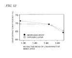
- the results of light extraction efficiency measurement are shown in FIG. 12 .
- the horizontal axis represents the refractive index of the low-refractive index layer 15 a
- the vertical axis represents light extraction efficiency.
- the extraction efficiency is higher in the case where a diffusion-type film is attached; however, when the refractive index of the low-refractive index layer 15 b is 1.45 or less, the efficiency is higher in the case where a microlens array film is attached.
- a construction where the low-refractive index layer has a refractive index which is lower than 1.45 and where a microlens array film is provided may be adopted.
- the bump-dent structure was diffraction grating with a period of 2 ⁇ m and a height of 0.6 ⁇ m.
- the Fourier modal method (RCWA method) was applied to the diffraction grating portion, and the results of this calculation and ray tracing results were taken in conjunction to calculate a light extraction efficiency of the entire organic EL device 100 .
- the results indicate that, in the case where the refractive index n1 of the transparent substrate 14 is 1.5, a higher light extraction efficiency is obtained by using a microlens array than a diffusing layer if the refractive index n2 of the low-refractive index layer 15 a is lower than 1.47.
- the refractive index n2 of the low-refractive index layer 15 a is set to a smaller value than 0.98 times the refractive index n1 of the transparent substrate 14 .
- certain effects will be obtained so long as the refractive index n2 of the low-refractive index layer 15 a is smaller than the refractive index n1 of the transparent substrate 4 .
- the experiment was directed to two kinds of devices including high-refractive index layers 15 b with refractive indices of 1.75 and 1.80, in a similar construction to that used in the experiment shown in FIG. 12 where the refractive index of the low-refractive index layer 15 a was 1.45 and the external light-extraction layer 16 was a microlens array. As FIG. 15 indicates, the light extraction efficiency increases as the refractive index of the high-refractive index layer 15 b increases.
- the refractive index of the high-refractive index layer 15 b may be set to 1.73 or above.
- the bump-dent structure at the boundary between the low-refractive index layer 15 a and the high-refractive index layer 15 b can be formed by, for example, forming bump-dent features on the low-refractive index layer 15 a , and thereafter filling up the dents and bumps with the high-refractive index material.
- the transparent electrode 13 , the organic emission layer 12 , and the reflection electrode 11 short-circuiting is likely to occur between the transparent electrode 13 and the reflection electrode 11 if the surface of the high-refractive index layer 15 b has poor planarity. In that case, the device may not be capable of being lit, thus resulting in a poor production yield during manufacture.
- a construction which can minimize the height of the bump-dent features, thus to ensure planarity after filling with the high-refractive index layer 15 b .
- lowering the height of the bump-dent structure in this manner also makes it possible to reduce the amounts of materials used of the low-refractive index layer 15 a and the high-refractive index layer 15 b , thus providing for low cost.
- the height (size) of the bump-dent structure needs to be at least on the order of 1 ⁇ 4 times the wavelength of light. This will ensure sufficient optical phase differences for diffracting light, whereby the light-extracting efficiency can be improved.
- a diffraction grating with a random structure or a periodic structure, etc., having a height (size) around 1 ⁇ m is adopted as an exemplary bump-dent structure.
- the thickness of the low-refractive index layer 15 a may be set to 1 ⁇ 2 times or more of the average emission wavelength.
- the material for the high-refractive index layer 15 b may be, for example: an inorganic material with a relatively high refractive index, e.g., ITO (indium tin oxide), TiO 2 (titanium oxide), SiN (silicon nitride), Ta 2 O 5 (tantalum pentoxide), or ZrO 2 (zirconia); a high-refractive index resin; or the like.
- ITO indium tin oxide
- TiO 2 titanium oxide
- SiN silicon nitride
- Ta 2 O 5 tantalum pentoxide
- ZrO 2 zirconia
- the transparent substrate 14 which have refractive indices on the order of 1.5 to 1.65. Therefore, as the material of the low-refractive index layer 15 a , inorganic materials such as glass and SiO 2 (quartz), and resins and the like can be used.
- a low-refractive index layer 15 a whose surface has bump-dent features may be formed on the transparent substrate 14 , for example, and the bump-dent structure may be filled up with a high-refractive index material from above, whereupon the transparent electrode 13 , the organic emission layer 12 , and the reflection electrode may be formed.
- the reflection electrode 11 may be formed on a substrate; the organic emission layer 12 , the transparent electrode 13 , and a high-refractive index layer 15 b whose surface has bump-dent features may be formed thereupon; the bump-dent structure may be filled with a low-refractive index material from above; and the transparent substrate 14 may be formed thereupon.
- the materials of the low-refractive index layer 15 a and the high-refractive index layer 15 b When inorganic materials are used as the materials of the low-refractive index layer 15 a and the high-refractive index layer 15 b , a relatively high-cost technique such as cutting or a semiconductor process will generally be required. On the other hand, when the aforementioned resin materials are used as the materials of the low-refractive index layer 15 a and the high-refractive index layer 15 b , it is possible to form the internal light-extraction layer 15 by a relatively low-cost technique, such as application, nanoimprint, and spin-coating.
- a relatively low-cost technique such as application, nanoimprint, and spin-coating.
- FIG. 16 shows changes in the transmittance of incident light at an incident angle of 40 degrees to 60 degrees when the amount of protrusion (height h) of the sphere of each microlens is varied.
- the vertical axis represents the average transmittance of light at an incident angle of 40 degrees to 60 degrees.
- the average transmittance increases as the aspect ratio increases, such that the structure with an aspect ratio of one (i.e., a structure with hemispheres) has the highest transmittance.
- the transmittance indicated by a broken line represents the value of average transmittance of light which is incident on the diffusion-type film at an incident angle of 40 degrees to 60 degrees as shown in FIG. 6B .
- the aspect ratio is 0.5 or above that a transmittance of 42% is exceeded at all.
- FIG. 17 is a graph showing incident angle dependence of light intensity per unit area in the cases where the aspect ratio is 0.33, 0.5, 0.67, 0.8 and 1.0. As this figure indicates, the light intensity peak at an incident angle of 40 degrees to 60 degrees becomes more conspicuous as the aspect ratio approaches 1.0.
- FIG. 19 is a graph showing results of this comparison.
- the horizontal axis represents incident angle
- the vertical axis represents light intensity per unit area.
- a solid line indicates results of the close-packed case illustrated in FIG. 5A ;
- a dotted line indicates results of the square arrangement illustrated in FIG. 18 ;
- a broken line indicates results where no microlens array is provided.
- the graph of FIG. 19 it is only the case under the close-packed microlenses that the transmittance of light at an incident angle of 40 degrees to 60 degrees becomes idiosyncratically large.
- the present embodiment has illustrated a microlens array as an example of the external light-extraction layer 16 .
- the microlens array in the present embodiment has a transmittance peak for light at incident angles ranging from 40 degrees to 60 degrees. Therefore, by combining a microlens array and the internal light-extraction layer 15 including the low-refractive index layer 15 a whose refractive index is relatively low, a higher efficiency can be provided over other constructions. Without being limited to a microlens array, this effect can be similarly obtained with any external light-extraction layer 16 that is arranged so that light arriving at an incident angle of 40 degrees to 60 degrees has a transmittance peak. Thus, a variant of the external light-extraction layer 16 will be described below.
- FIG. 20A is a plan view showing pyramidal structures as a similar configuration to a microlens array.
- FIG. 20B is a cross-sectional view taken along line B-B′ in FIG. 20A .
- FIG. 21 is a graph showing dependence of an average value of transmittance of light at an incident angle from 40 to 60 degrees on the vertex angle of each pyramidal structure.
- FIG. 22 is a graph showing incident angle dependence of light intensity per unit area in the respective cases where each pyramidal structure has vertex angles of 30 degrees, 50 degrees, 70 degrees, 90 degrees, 110 degrees, 130 degrees and 150 degrees. From these results, too, it can be seen that light at an incident angle of 40 degrees to 60 degrees has a relatively high average transmittance when the vertex angle is in the range from 30 degrees to 120 degrees. Therefore, in the case of adopting a pyramidal-structured array for the external light-extraction layer 16 , the vertex angle may be set in a range from 30 degrees to 120 degrees.
- a bump-dent structure with controlled randomness can be adopted.
- a “structure with controlled randomness” means a structure whose randomness is reduced so that no blocks of the same kind successively appear a predetermined number of times or more along one direction, rather than a completely random structure. As has been described with reference to FIG. 8A , by adopting a bump-dent structure with controlled randomness, it becomes possible to further improve the light extraction efficiency.
- an average period can be determined based on a similar principle to the above.
- a method of determining an average period from the pattern of a structure is shown in FIG. 24 .
- Ellipses will now be considered, each being inscribed in a region consisting of successive unit structures of the same kind, with respect to both of the lateral direction and the vertical direction in FIG. 24 .
- an average value of the sizes of the white portions can be determined by calculating an average value of the axial lengths of ellipses which are inscribed in the white portions.
- an “axial length” refers to the length a of the minor axis or the length b of the major axis as illustrated in the upper diagram of FIG. 24 .
- An average period is defined by a value obtained by taking a sum of these average values.
- FIGS. 25 ( a ) to ( c ) are diagrams showing examples of bump-dent structures with controlled randomness (with average periods of 3w, 3.3w and 3.4w, respectively).
- a bump-dent structure may be a structure including an array of blocks of shapes other than squares, e.g., hexagons.
- FIG. 26 is a graph showing results of calculating dependence of light extraction efficiency on the width w of the bump-dent features.
- the height h of the structure is 1.0 ⁇ m.
- the transparent substrate 14 has a refractive index of 1.5; the low-refractive index layer 15 a has a refractive index of 1.35; and the high-refractive index layer 15 b has a refractive index of 2.0.
- ( ⁇ ) indicates results when adopting bump-dent features composed of randomly-arrayed blocks as shown in FIG. 23( a )
- ( ⁇ ) indicates results when adopting bump-dent features composed of periodically-arrayed blocks as shown in FIG. 23( b ) .
- a light extraction efficiency of 69% or more can be obtained so long as w is in the range from 0.4 to 2 ⁇ m.
- a light extraction efficiency of 69% or more can be obtained so long as w is in the range from 0.4 to 4 ⁇ m.
- a light extraction efficiency of 69% or more can be obtained by setting w to 2 ⁇ m or less for a random structure, or setting w to 4 ⁇ m or less for a periodic structure.
- the average period, p may be set to 8 ⁇ m or less, for example.
- a periodic structure will have large wavelength dependence due to the nature of a diffraction grating, thus resulting in a large color unevenness with respect to the viewing angle. Therefore, in order to reduce color unevenness with respect to the viewing angle, features composed of randomly arrayed structures may be adopted as the bump-dent features.
- FIG. 28 is a graph showing results thereof.
- ( ⁇ )( ⁇ )( ⁇ ) represent results of calculations performed for the corresponding random structures in FIG. 27 .
- the transparent substrate 14 had a refractive index of 1.51; the low-refractive index layer 15 a had a refractive index of 1.45; and the high-refractive index layer 15 b had a refractive index of 1.76.
- ( ⁇ ) structure rectangular solids with a structure size of 0.6 ⁇ m and a height of 0.2 to 0.8 ⁇ m are randomly arrayed.
- rectangular solids with a structure size of 1.2 ⁇ m and a height of 0.6 ⁇ m are randomly arrayed. However, their randomness is controlled so that no three or more blocks successively appear along the same direction.
- hexagonal columns with a structure size (diameter of a circle inscribed in a hexagon) 1.2 ⁇ m and a height of 0.6 to 1.2 ⁇ m are randomly arrayed. However, their randomness is controlled so that no four or more blocks successively appear along the same direction.
- FIG. 30 is a diagram showing amplitude of spatial frequency components when applying a Fourier transform to a random pattern.
- the center of a distribution diagram on the right-hand side of FIG. 30 shows a component whose spatial frequency is zero (DC component). This diagram is illustrated so that spatial frequency increases from the center toward the outside.
- DC component whose spatial frequency is zero
- a bump-dent structure is created by arraying blocks of the same size; with a random array of these, the light extraction efficiency becomes high when w is set to a value in a range from 0.4 to 2 ⁇ m, as shown in FIG. 26 . Based on this, it would also be applicable to randomly array a plurality of blocks whose size is appropriately altered within this range.
- FIG. 31 is a perspective view showing an exemplary construction in which random block heights are adopted.
- the bump-dent structure 166 shown in the figure includes a random two-dimensional array of first unit structures 166 a of a first height, second unit structures 166 b of a second height, third unit structures 166 c of a third height, and fourth unit structures 166 d of a fourth height.
- each block is filled with a high-refractive index material and a low-refractive index material, so that differences occur in the phase of light which travels through these portions. Therefore, even in the case of random heights, an average phase difference of transmitted light is to be determined by an average height of the plurality of unit structures, such that a sufficient average phase difference will be imparted to the transmitted light also in this case. Thus, random heights may be adopted.
- each cross-sectional shape may be rounded.
- the corner portions are processed so as to be rounded, or stepped portions are processed into slopes. If these factors arise when processing the bump-dent structure of the internal light-extraction layer 15 , any structure with corner portions being processed so as to be rounded is also encompassed within the present construction, so long as the aforementioned properties of a random pattern are not lost.
- a high-refractive index hemispherical lens was placed on the high-refractive index layer 15 b of the organic EL device 100 to measure an angular distribution of emission intensity of the emission layer 12 .
- Three kinds of organic EL devices were prototyped in which an emission layer 12 with an emission wavelength of 580 nm was layered. The emission points of these elements were respectively set at positions of 70, 90 and 290 nm from the surface of the reflection electrode 11 .
- the high-refractive index layer 15 b and the high-refractive index hemispherical lens had a refractive index of 1.77. For comparison's sake, a simulation was also conducted.
- the results of measurement and the results of calculation are shown in FIG. 33A and FIG. 33B .
- the results of the cases where the distance from the surface of the reflection electrode 11 was 160 nm or less are shown in FIG. 33A , while the results of the cases where this distance was 200 nm or more are shown in FIG. 33B .
- the experimental results and the measurement results match well.
- the position of the emission point is 90 nm or less, there is hardly any light of 60 degrees or more. This indicates that, when the distance between the transparent electrode 13 and the surface of the reflection electrode 11 is small, light on the higher angle side combines with a surface plasmon on the reflection electrode, thus becoming lost.
- the critical angle of the light propagating from the emission layer 12 to the transparent substrate 14 is approximately 60 degrees. Therefore, in the case where light of 60 degrees or more is absent, there is no need to internally provide a light extraction structure, to begin with.
- FIG. 34 shows results of calculating dependence of emission efficiency on the distance between the emission point and the reflection electrode 11 .
- the emission efficiency is 60% or less, indicating that 40% or more of the light has combined with a surface plasmon to become lost.
- efficiency enhancement has its limits.
- the internal light-extraction layer 15 was introduced.
- An angular distribution of light intensity within the transparent substrate 14 after passage through the internal light-extraction layer 15 was calculated. The results of calculation are shown in FIG. 35 .
- the transparent substrate 14 had a refractive index of 1.51
- the low-refractive index layer 15 a had a refractive index of 1.45
- the high-refractive index layer 15 b had a refractive index of 1.76
- the bump-dent structure was a random structure.
- FIG. 36 shows, among the calculation results, results of plotting the total amount of light with incident angles falling within the respective ranges of 0° to 20°, 20° to 40°, and 40° to 60°, against the distance between the emission point and the surface of the reflection electrode 11 .
- the light-emitting element 110 in the above embodiment emits light through organic EL
- other light-emitting elements e.g., inorganic EL
- the light-emitting element 110 may have any arbitrary construction so long as a light extraction sheet 120 including the internal light-extraction layer 15 , the transparent substrate 14 , and the external light-extraction layer 16 is provided.
- an electrode which lacks a light-reflecting property may be used.
- An illuminator according to the present disclosure is applicable to flat panel displays, backlights for liquid crystal display devices, light sources for illumination, etc., for example.
- a light extraction sheet according to the present disclosure is applicable to the aforementioned illuminator.
Applications Claiming Priority (3)
| Application Number | Priority Date | Filing Date | Title |
|---|---|---|---|
| JP2013-084132 | 2013-04-12 | ||
| JP2013084132 | 2013-04-12 | ||
| PCT/JP2014/000220 WO2014167758A1 (ja) | 2013-04-12 | 2014-01-17 | 発光装置 |
Publications (2)
| Publication Number | Publication Date |
|---|---|
| US20160049562A1 US20160049562A1 (en) | 2016-02-18 |
| US9595648B2 true US9595648B2 (en) | 2017-03-14 |
Family
ID=51689182
Family Applications (1)
| Application Number | Title | Priority Date | Filing Date |
|---|---|---|---|
| US14/783,239 Active US9595648B2 (en) | 2013-04-12 | 2014-01-17 | Light-emitting device |
Country Status (6)
| Country | Link |
|---|---|
| US (1) | US9595648B2 (zh) |
| EP (1) | EP2986082A4 (zh) |
| JP (1) | JP6471905B2 (zh) |
| KR (1) | KR20150141955A (zh) |
| CN (1) | CN105027671B (zh) |
| WO (1) | WO2014167758A1 (zh) |
Cited By (2)
| Publication number | Priority date | Publication date | Assignee | Title |
|---|---|---|---|---|
| US11036073B2 (en) | 2017-08-08 | 2021-06-15 | Samsung Electronics Co., Ltd. | Optical member, polarization member, and display device |
| US11864547B2 (en) * | 2017-01-10 | 2024-01-09 | Seoul Viosys Co., Ltd. | Adhesive-type insect trap having a cover with a light refracting portion formed thereon |
Families Citing this family (21)
| Publication number | Priority date | Publication date | Assignee | Title |
|---|---|---|---|---|
| WO2014188631A1 (ja) * | 2013-05-21 | 2014-11-27 | パナソニックIpマネジメント株式会社 | 発光装置 |
| DE102015102365A1 (de) * | 2015-02-19 | 2016-08-25 | Osram Opto Semiconductors Gmbh | Strahlungskörper und Verfahren zur Herstellung eines Strahlungskörpers |
| CN106935733B (zh) * | 2015-12-31 | 2019-05-17 | 昆山工研院新型平板显示技术中心有限公司 | 柔性显示装置及其制作方法 |
| JP6620035B2 (ja) * | 2016-02-25 | 2019-12-11 | 株式会社ジャパンディスプレイ | 表示装置 |
| CN105914275B (zh) * | 2016-06-22 | 2018-04-27 | 天津三安光电有限公司 | 倒装发光二极管及其制作方法 |
| CN106684256A (zh) * | 2016-12-23 | 2017-05-17 | 上海天马有机发光显示技术有限公司 | 一种显示面板及其制作方法 |
| WO2019003058A1 (en) * | 2017-06-26 | 2019-01-03 | 3M Innovative Properties Company | STRUCTURED FILM AND ARTICLES THEREFOR |
| US10153461B1 (en) * | 2017-09-13 | 2018-12-11 | Int Tech Co., Ltd. | Display panel and method for manufacturing the same |
| CN107808934A (zh) * | 2017-11-30 | 2018-03-16 | 武汉天马微电子有限公司 | 有机发光显示面板和显示装置 |
| EP3785307A1 (en) * | 2018-04-23 | 2021-03-03 | Cree, Inc. | Semiconductor light emitting devices including superstrates with patterned surfaces |
| CN109638175A (zh) * | 2018-11-30 | 2019-04-16 | 武汉华星光电半导体显示技术有限公司 | 有机发光装置及阵列基板 |
| US11315982B2 (en) * | 2018-12-05 | 2022-04-26 | Boe Technology Group Co., Ltd. | Light emitting diode with a patterned scattering layer and fabrication method thereof, display substrate and display panel |
| US11302248B2 (en) | 2019-01-29 | 2022-04-12 | Osram Opto Semiconductors Gmbh | U-led, u-led device, display and method for the same |
| US11156759B2 (en) | 2019-01-29 | 2021-10-26 | Osram Opto Semiconductors Gmbh | μ-LED, μ-LED device, display and method for the same |
| US11610868B2 (en) | 2019-01-29 | 2023-03-21 | Osram Opto Semiconductors Gmbh | μ-LED, μ-LED device, display and method for the same |
| US11271143B2 (en) | 2019-01-29 | 2022-03-08 | Osram Opto Semiconductors Gmbh | μ-LED, μ-LED device, display and method for the same |
| US11538852B2 (en) | 2019-04-23 | 2022-12-27 | Osram Opto Semiconductors Gmbh | μ-LED, μ-LED device, display and method for the same |
| KR20220009426A (ko) * | 2019-05-14 | 2022-01-24 | 오스람 옵토 세미컨덕터스 게엠베하 | 조명 유닛, 조명 유닛을 제조하기 위한 방법, 광전자 부품을 위한 변환체 요소, led 및 변환체 요소를 갖는 복사선 소스, 커플링-아웃 구조, 및 광전자 장치 |
| CN113851573B (zh) * | 2021-09-23 | 2023-09-01 | 深圳迈塔兰斯科技有限公司 | 提高发光二极管取光效率的超表面 |
| CN113964280B (zh) * | 2021-10-18 | 2024-04-16 | 湖北长江新型显示产业创新中心有限公司 | 显示面板及显示装置 |
| CN114335389B (zh) * | 2021-12-30 | 2024-01-26 | 湖北长江新型显示产业创新中心有限公司 | 显示面板及显示装置 |
Citations (16)
| Publication number | Priority date | Publication date | Assignee | Title |
|---|---|---|---|---|
| JPH04328295A (ja) | 1991-04-26 | 1992-11-17 | Pioneer Electron Corp | 有機エレクトロルミネッセンス素子 |
| JP2991183B2 (ja) | 1998-03-27 | 1999-12-20 | 日本電気株式会社 | 有機エレクトロルミネッセンス素子 |
| JP2003100444A (ja) | 2001-09-26 | 2003-04-04 | Keiwa Inc | 面照明装置 |
| JP2004241130A (ja) | 2003-02-03 | 2004-08-26 | Seiko Epson Corp | 発光ディスプレイパネルおよびその製造方法 |
| JP2006190573A (ja) | 2005-01-06 | 2006-07-20 | Toshiba Corp | 有機エレクトロルミネッセンス素子およびその製造方法 |
| US20080197764A1 (en) | 2005-05-12 | 2008-08-21 | Koninklijke Philips Electronics, N.V. | Electroluminescence Light Source |
| JP2009272059A (ja) | 2008-04-30 | 2009-11-19 | Toppan Printing Co Ltd | El素子、el素子を用いた液晶ディスプレイ用バックライト装置、el素子を用いた照明装置、el素子を用いた電子看板装置、及びel素子を用いたディスプレイ装置 |
| WO2010051229A2 (en) | 2008-10-31 | 2010-05-06 | 3M Innovative Properties Company | Light extraction film with high index backfill layer and passivation layer |
| US20110080737A1 (en) | 2009-05-12 | 2011-04-07 | Seiji Nishiwaki | Sheet, light emitting device, and method for producing the sheet |
| WO2012108384A1 (ja) | 2011-02-10 | 2012-08-16 | シャープ株式会社 | 蛍光体基板、およびこれを用いた表示装置、照明装置 |
| US20120248970A1 (en) * | 2011-04-04 | 2012-10-04 | Rohm Co., Ltd. | Organic el device |
| US20120286258A1 (en) | 2010-04-22 | 2012-11-15 | Idemitsu Kosan Co., Ltd. | Organic electroluminescent element and lighting device |
| US20120292652A1 (en) | 2010-01-19 | 2012-11-22 | Panasonic Corporation | Surface light emitting device |
| US20130015486A1 (en) | 2010-04-02 | 2013-01-17 | Koujirou Sekine | Organic light-emitting element |
| US9184404B2 (en) | 2011-03-24 | 2015-11-10 | Panasonic Intellectual Property Management Co., Ltd. | White light-emitting organic electroluminescent element and white light-emitting organic electroluminescent panel |
| US20160141554A1 (en) * | 2013-05-21 | 2016-05-19 | Panasonic Intellectual Property Management Co., Ltd. | Light emitting apparatus |
-
2014
- 2014-01-17 EP EP14783361.0A patent/EP2986082A4/en not_active Withdrawn
- 2014-01-17 KR KR1020157028203A patent/KR20150141955A/ko not_active Application Discontinuation
- 2014-01-17 JP JP2015511078A patent/JP6471905B2/ja active Active
- 2014-01-17 WO PCT/JP2014/000220 patent/WO2014167758A1/ja active Application Filing
- 2014-01-17 CN CN201480005446.1A patent/CN105027671B/zh not_active Expired - Fee Related
- 2014-01-17 US US14/783,239 patent/US9595648B2/en active Active
Patent Citations (23)
| Publication number | Priority date | Publication date | Assignee | Title |
|---|---|---|---|---|
| JPH04328295A (ja) | 1991-04-26 | 1992-11-17 | Pioneer Electron Corp | 有機エレクトロルミネッセンス素子 |
| JP2991183B2 (ja) | 1998-03-27 | 1999-12-20 | 日本電気株式会社 | 有機エレクトロルミネッセンス素子 |
| US20020180348A1 (en) | 1998-03-27 | 2002-12-05 | Atsushi Oda | Organic electroluminescent device with a defraction grading and luminescent layer |
| JP2003100444A (ja) | 2001-09-26 | 2003-04-04 | Keiwa Inc | 面照明装置 |
| JP2004241130A (ja) | 2003-02-03 | 2004-08-26 | Seiko Epson Corp | 発光ディスプレイパネルおよびその製造方法 |
| US20040189185A1 (en) | 2003-02-03 | 2004-09-30 | Shinichi Yotsuya | Light emitting display panel and method of manufacturing the same |
| JP2006190573A (ja) | 2005-01-06 | 2006-07-20 | Toshiba Corp | 有機エレクトロルミネッセンス素子およびその製造方法 |
| US20060192483A1 (en) | 2005-01-06 | 2006-08-31 | Tsutomu Nakanishi | Organic electroluminescent device |
| US20080197764A1 (en) | 2005-05-12 | 2008-08-21 | Koninklijke Philips Electronics, N.V. | Electroluminescence Light Source |
| JP2008541368A (ja) | 2005-05-12 | 2008-11-20 | コーニンクレッカ フィリップス エレクトロニクス エヌ ヴィ | エレクトロルミネッセンス光源 |
| JP2009272059A (ja) | 2008-04-30 | 2009-11-19 | Toppan Printing Co Ltd | El素子、el素子を用いた液晶ディスプレイ用バックライト装置、el素子を用いた照明装置、el素子を用いた電子看板装置、及びel素子を用いたディスプレイ装置 |
| WO2010051229A2 (en) | 2008-10-31 | 2010-05-06 | 3M Innovative Properties Company | Light extraction film with high index backfill layer and passivation layer |
| US20100110551A1 (en) | 2008-10-31 | 2010-05-06 | 3M Innovative Properties Company | Light extraction film with high index backfill layer and passivation layer |
| US20110080737A1 (en) | 2009-05-12 | 2011-04-07 | Seiji Nishiwaki | Sheet, light emitting device, and method for producing the sheet |
| US20120292652A1 (en) | 2010-01-19 | 2012-11-22 | Panasonic Corporation | Surface light emitting device |
| US20130015486A1 (en) | 2010-04-02 | 2013-01-17 | Koujirou Sekine | Organic light-emitting element |
| EP2555587A1 (en) | 2010-04-02 | 2013-02-06 | Konica Minolta Holdings, Inc. | Organic light-emitting element |
| US20120286258A1 (en) | 2010-04-22 | 2012-11-15 | Idemitsu Kosan Co., Ltd. | Organic electroluminescent element and lighting device |
| WO2012108384A1 (ja) | 2011-02-10 | 2012-08-16 | シャープ株式会社 | 蛍光体基板、およびこれを用いた表示装置、照明装置 |
| US9184404B2 (en) | 2011-03-24 | 2015-11-10 | Panasonic Intellectual Property Management Co., Ltd. | White light-emitting organic electroluminescent element and white light-emitting organic electroluminescent panel |
| US20120248970A1 (en) * | 2011-04-04 | 2012-10-04 | Rohm Co., Ltd. | Organic el device |
| JP2012227122A (ja) | 2011-04-04 | 2012-11-15 | Rohm Co Ltd | 有機el装置 |
| US20160141554A1 (en) * | 2013-05-21 | 2016-05-19 | Panasonic Intellectual Property Management Co., Ltd. | Light emitting apparatus |
Non-Patent Citations (3)
| Title |
|---|
| PCT Search Report issued by the Japanese Patent Office in PCT/JP2014/000220, dated Apr. 22, 2014. |
| Search Report issued in European Patent Office (EPO) Patent Application No. 14783361.0, dated Apr. 7, 2016. |
| U.S. Appl. No. 14/772,599 to Kazuyuki Yamae et al., which was filed Sep. 3, 2015. |
Cited By (2)
| Publication number | Priority date | Publication date | Assignee | Title |
|---|---|---|---|---|
| US11864547B2 (en) * | 2017-01-10 | 2024-01-09 | Seoul Viosys Co., Ltd. | Adhesive-type insect trap having a cover with a light refracting portion formed thereon |
| US11036073B2 (en) | 2017-08-08 | 2021-06-15 | Samsung Electronics Co., Ltd. | Optical member, polarization member, and display device |
Also Published As
| Publication number | Publication date |
|---|---|
| KR20150141955A (ko) | 2015-12-21 |
| CN105027671A (zh) | 2015-11-04 |
| JP6471905B2 (ja) | 2019-02-20 |
| CN105027671B (zh) | 2017-09-22 |
| JPWO2014167758A1 (ja) | 2017-02-16 |
| EP2986082A1 (en) | 2016-02-17 |
| US20160049562A1 (en) | 2016-02-18 |
| WO2014167758A1 (ja) | 2014-10-16 |
| EP2986082A4 (en) | 2016-05-11 |
Similar Documents
| Publication | Publication Date | Title |
|---|---|---|
| US9595648B2 (en) | Light-emitting device | |
| JP5866552B2 (ja) | 有機エレクトロルミネッセンス素子及びそれを用いた照明装置 | |
| US10756304B2 (en) | Organic light-emitting display panel and display device thereof | |
| JP5830194B2 (ja) | 有機エレクトロルミネッセンス素子及びそれを用いた照明装置 | |
| US7498735B2 (en) | OLED device having improved power distribution | |
| US8987767B2 (en) | Light emitting device having improved light extraction efficiency | |
| US10269777B2 (en) | Display apparatus comprising reflection structure | |
| JP2015144110A (ja) | 発光装置 | |
| WO2014020901A1 (ja) | 光学シート、発光装置、光学シートの製造方法及び発光装置の製造方法 | |
| JP2010272515A (ja) | 有機電界発光表示装置 | |
| US9647240B2 (en) | Light emitting apparatus | |
| US20210399263A1 (en) | Multiple qd-led sub-pixels for high on-axis brightness and low colour shift | |
| KR102608318B1 (ko) | 유기발광장치 | |
| US9774006B2 (en) | Radiation-emitting apparatus having a scatter layer | |
| US8492967B2 (en) | Light emitting device and display panel | |
| KR102293473B1 (ko) | 유기 발광 표시 장치 및 유기 발광 표시 장치 제조 방법 | |
| US11956994B2 (en) | OLED light field architectures | |
| WO2015115045A1 (ja) | 発光装置および光取り出しシート | |
| JP2006107745A (ja) | 有機el表示装置 | |
| WO2015097971A1 (ja) | 発光装置 |
Legal Events
| Date | Code | Title | Description |
|---|---|---|---|
| AS | Assignment |
Owner name: PANASONIC INTELLECTUAL PROPERTY MANAGEMENT CO., LT Free format text: ASSIGNMENT OF ASSIGNORS INTEREST;ASSIGNORS:INADA, YASUHISA;YAMAE, KAZUYUKI;HASHIYA, AKIRA;REEL/FRAME:037205/0973 Effective date: 20150515 |
|
| STCF | Information on status: patent grant |
Free format text: PATENTED CASE |
|
| MAFP | Maintenance fee payment |
Free format text: PAYMENT OF MAINTENANCE FEE, 4TH YEAR, LARGE ENTITY (ORIGINAL EVENT CODE: M1551); ENTITY STATUS OF PATENT OWNER: LARGE ENTITY Year of fee payment: 4 |
|
| AS | Assignment |
Owner name: SAMSUNG DISPLAY CO., LTD., KOREA, REPUBLIC OF Free format text: ASSIGNMENT OF ASSIGNORS INTEREST;ASSIGNOR:PANASONIC INTELLECTUAL PROPERTY MANAGEMENT CO., LTD.;REEL/FRAME:058549/0122 Effective date: 20211130 |