US9594205B2 - Backlight module, display comprising the same and method for manufacturing light guiding plate - Google Patents
Backlight module, display comprising the same and method for manufacturing light guiding plate Download PDFInfo
- Publication number
- US9594205B2 US9594205B2 US14/607,125 US201514607125A US9594205B2 US 9594205 B2 US9594205 B2 US 9594205B2 US 201514607125 A US201514607125 A US 201514607125A US 9594205 B2 US9594205 B2 US 9594205B2
- Authority
- US
- United States
- Prior art keywords
- curve
- light
- distances
- guiding plate
- backlight module
- Prior art date
- Legal status (The legal status is an assumption and is not a legal conclusion. Google has not performed a legal analysis and makes no representation as to the accuracy of the status listed.)
- Active, expires
Links
Images


Classifications
-
- G—PHYSICS
- G02—OPTICS
- G02B—OPTICAL ELEMENTS, SYSTEMS OR APPARATUS
- G02B6/00—Light guides; Structural details of arrangements comprising light guides and other optical elements, e.g. couplings
- G02B6/0001—Light guides; Structural details of arrangements comprising light guides and other optical elements, e.g. couplings specially adapted for lighting devices or systems
- G02B6/0011—Light guides; Structural details of arrangements comprising light guides and other optical elements, e.g. couplings specially adapted for lighting devices or systems the light guides being planar or of plate-like form
- G02B6/0033—Means for improving the coupling-out of light from the light guide
- G02B6/0035—Means for improving the coupling-out of light from the light guide provided on the surface of the light guide or in the bulk of it
- G02B6/0045—Means for improving the coupling-out of light from the light guide provided on the surface of the light guide or in the bulk of it by shaping at least a portion of the light guide
-
- B—PERFORMING OPERATIONS; TRANSPORTING
- B29—WORKING OF PLASTICS; WORKING OF SUBSTANCES IN A PLASTIC STATE IN GENERAL
- B29D—PRODUCING PARTICULAR ARTICLES FROM PLASTICS OR FROM SUBSTANCES IN A PLASTIC STATE
- B29D11/00—Producing optical elements, e.g. lenses or prisms
- B29D11/00663—Production of light guides
- B29D11/00721—Production of light guides involving preforms for the manufacture of light guides
-
- G—PHYSICS
- G02—OPTICS
- G02B—OPTICAL ELEMENTS, SYSTEMS OR APPARATUS
- G02B6/00—Light guides; Structural details of arrangements comprising light guides and other optical elements, e.g. couplings
- G02B6/0001—Light guides; Structural details of arrangements comprising light guides and other optical elements, e.g. couplings specially adapted for lighting devices or systems
- G02B6/0011—Light guides; Structural details of arrangements comprising light guides and other optical elements, e.g. couplings specially adapted for lighting devices or systems the light guides being planar or of plate-like form
- G02B6/0033—Means for improving the coupling-out of light from the light guide
- G02B6/0035—Means for improving the coupling-out of light from the light guide provided on the surface of the light guide or in the bulk of it
- G02B6/0036—2-D arrangement of prisms, protrusions, indentations or roughened surfaces
-
- G—PHYSICS
- G02—OPTICS
- G02B—OPTICAL ELEMENTS, SYSTEMS OR APPARATUS
- G02B6/00—Light guides; Structural details of arrangements comprising light guides and other optical elements, e.g. couplings
- G02B6/0001—Light guides; Structural details of arrangements comprising light guides and other optical elements, e.g. couplings specially adapted for lighting devices or systems
- G02B6/0011—Light guides; Structural details of arrangements comprising light guides and other optical elements, e.g. couplings specially adapted for lighting devices or systems the light guides being planar or of plate-like form
- G02B6/0033—Means for improving the coupling-out of light from the light guide
- G02B6/0035—Means for improving the coupling-out of light from the light guide provided on the surface of the light guide or in the bulk of it
- G02B6/0038—Linear indentations or grooves, e.g. arc-shaped grooves or meandering grooves, extending over the full length or width of the light guide
-
- G—PHYSICS
- G02—OPTICS
- G02B—OPTICAL ELEMENTS, SYSTEMS OR APPARATUS
- G02B6/00—Light guides; Structural details of arrangements comprising light guides and other optical elements, e.g. couplings
- G02B6/0001—Light guides; Structural details of arrangements comprising light guides and other optical elements, e.g. couplings specially adapted for lighting devices or systems
- G02B6/0011—Light guides; Structural details of arrangements comprising light guides and other optical elements, e.g. couplings specially adapted for lighting devices or systems the light guides being planar or of plate-like form
- G02B6/0033—Means for improving the coupling-out of light from the light guide
- G02B6/0058—Means for improving the coupling-out of light from the light guide varying in density, size, shape or depth along the light guide
-
- G—PHYSICS
- G02—OPTICS
- G02B—OPTICAL ELEMENTS, SYSTEMS OR APPARATUS
- G02B6/00—Light guides; Structural details of arrangements comprising light guides and other optical elements, e.g. couplings
- G02B6/0001—Light guides; Structural details of arrangements comprising light guides and other optical elements, e.g. couplings specially adapted for lighting devices or systems
- G02B6/0011—Light guides; Structural details of arrangements comprising light guides and other optical elements, e.g. couplings specially adapted for lighting devices or systems the light guides being planar or of plate-like form
- G02B6/0065—Manufacturing aspects; Material aspects
-
- G—PHYSICS
- G02—OPTICS
- G02B—OPTICAL ELEMENTS, SYSTEMS OR APPARATUS
- G02B6/00—Light guides; Structural details of arrangements comprising light guides and other optical elements, e.g. couplings
- G02B6/0001—Light guides; Structural details of arrangements comprising light guides and other optical elements, e.g. couplings specially adapted for lighting devices or systems
- G02B6/0011—Light guides; Structural details of arrangements comprising light guides and other optical elements, e.g. couplings specially adapted for lighting devices or systems the light guides being planar or of plate-like form
- G02B6/0081—Mechanical or electrical aspects of the light guide and light source in the lighting device peculiar to the adaptation to planar light guides, e.g. concerning packaging
- G02B6/0093—Means for protecting the light guide
Definitions
- the present invention relates to a backlight module, a display comprising the same and a method for manufacturing a light guiding plate, and particularly to a backlight module having a special pattern, to reduce the dose of light source, solve the problem of collimated light in the conventional backlight module, and reduce the manufacturing cost of the backlight module.
- a backlight module is an indispensable element of a display device, usually composed of a backboard, a light guide plate, a light source and multiple optical films.
- the light source spacing and the distance between the dots should also be considered. If the light source spacing is small, multiple light sources are required, thereby increasing the cost; however, if the light source spacing is large, the hotspot problem will be an issue due to the reduced number of the light source, thereby detrimentally affecting the luminous quality.
- the light entrance side close to the light source is cut out an R-cut or a V-cut.
- an extrusion light guide plate it is less economical for an extrusion light guide plate to be cut out an R-cut or a V-cut on a cutting board.
- a lenticular layer is typically added on the light guide plate to solve this problem.
- an injection light guide plate may be made with the R-cut or V-cut, it is not easy to make a thin injection light guide plate, and it remains an obstacle to miniaturization.
- the combination of the light guide plate and the lenticular layer can improve light divergence uniformity of the backlight module and reduce the manufacturing costs, it will cause the backlight module to have collimated light phenomenon, thereby degrading aesthetic.
- a backlight module can be provided, which can solve hotspot and collimated light problems and reduces the manufacturing costs at the same time, it would represent a new milestone in the development of the backlight module technology.
- An object of the present invention is to provide a backlight module and a method for manufacturing a light guide plate in the backlight module, so as to form a special structure pattern on the light guide plate, to destroy the proceeding of the collimated light, thereby fulfilling the requirements of the light divergence uniformity and aesthetic appearance.
- Another object of the present invention is to provide a display that includes the backlight module of the present invention, in order to provide the display with better display quality.
- the present invention provides a backlight module, comprising: a housing; a light guiding plate disposed in the housing, and light guiding plate comprises a light entrance surface, a bottom surface, and a light exit surface, wherein the bottom surface and the light exit surface are spaced apart and disposed opposite to each other, and two opposite sides of the light entrance surface are connected to the bottom surface and the light exit surface respectively, wherein a direction parallel to the light entrance surface is defined as a horizontal direction, and a direction vertical to the light entrance surface is defined as a vertical direction; and a light source disposed adjacent the light entrance surface of the light guiding plate, wherein a horizontal cross section of the light exit surface of the light guiding plate has a first curve, and a vertical cross section of the light exit surface of the light guiding plate through any peak of the first curve has a second curve, wherein adjacent peaks of the first curve have a same distance therebetween, and adjacent troughs of the first curve are spaced apart by first distances, wherein any two adjacent first
- the application field of the backlight module according to the present invention is not particularly limited, and for example, it can be used in a monitor, a notebook computer, a digital camera, a projector and so on.
- the present invention also provides a method for manufacturing a light guide plate in the backlight module, comprising the following steps:
- step (c) translating the round knife along the first direction of the substrate to a distance, and performing the step (b) to form a plurality of mirroring second curves;
- step (d) repeating the step (c), so that a cross-sectional of the substrate in the first direction forms a mirroring first curve to produce a template
- the present invention still provides a display device comprising: the backlight module of the present invention; and a display panel disposed at a side of the light exit surface of the light guide plate.
- FIG. 1 shows a schematic diagram of the backlight module according to embodiments of the present invention.
- FIGS. 2A to 2C show a manufacturing flow chart of the template of the light guide plate according to the present invention.
- FIG. 3 shows a schematic diagram of the cylindrical template according to embodiments of the present invention.
- FIG. 4 shows a perspective view of the light guide plate according to embodiments of the present invention.
- FIG. 5 shows a cross sectional view of FIG. 4 in a horizontal direction.
- FIG. 6 shows a top view of FIG. 4 .
- FIG. 7 shows a cross sectional view along the section line a-a′ of FIG. 6 .
- FIG. 8 shows a schematic diagram of the display according to embodiments of the present invention.
- FIG. 1 shows a schematic diagram of the backlight module according to embodiments of the present invention.
- the steps for manufacturing the backlight are described as follows. First, a housing 1 , a light guide plate 2 and a light source 3 are provided, and a plurality of light emitting diodes (LED) are used as the light source in this embodiment.
- the light guide plate 2 is formed in the housing 1 and includes a light entrance surface 23 , a bottom surface 24 and a light exit surface 25 , wherein the bottom surface 24 and the light exit surface 25 are spaced apart and disposed opposite to each other, and two opposite sides of the light entrance surface 23 are connected to the bottom surface 24 and the light exit surface 25 respectively.
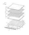
- the light source 3 is formed on the light entrance surface 23 of the light guiding plate 2 , wherein a direction parallel to the light entrance surface 23 is defined as a horizontal direction X, and a direction vertical to the light entrance surface 23 is defined as a vertical direction Y. Then, an optical layer 4 is formed on the light guide plate 2 to prepare a backlight module, wherein the optical layer 4 according to this embodiment is formed by sequentially laminating a diffusion layer 41 , a first prism layer 42 , a second prism layer 43 and a diffusion sheet 44 on the light guide plate 2 .
- the backlight module obtained by the above process comprises: a housing 1 ; a light guiding plate 2 comprising a light entrance surface 23 , a bottom surface 24 , and a light exit surface 25 , wherein the bottom surface 24 and the light exit surface 25 are spaced apart and disposed opposite to each other, and two opposite sides of the light entrance surface 23 are connected to the bottom surface 24 and the light exit surface 25 respectively; at least a light source 3 disposed adjacent the light entrance surface 23 of the light guiding plate 2 ; and at least an optical layer 4 disposed on the light guide plate 2 .
- the light emitted from the light guide plate 2 and the light emitted from the optical layer 4 do not interfere with each other.
- the light guide plate of the above-described embodiment may be formed by an imprinting process using a template.
- FIGS. 2A to 2C show a manufacturing flow chart of the template of the light guide plate according to the present invention.
- the method for manufacturing the template includes: (a) providing a substrate 5 and a round knife 6 having a fixed radius of curvature of 5 ⁇ m to 100 ⁇ m, wherein the substrate 5 has a first direction I and a second direction II perpendicular to the first direction I; (b) translating the round knife 6 along the second direction II of the substrate 5 , while moving the round knife 6 vertically with respect to the substrate 5 , so that a moving path of a vertex of the round knife 6 forms a mirroring second curve.
- step (c) translating the round knife 6 along the first direction I of the substrate 5 to a distance D4, and performing the step (b) to form a plurality of different mirroring second curves 52 ; (d) repeating the step (c), so that a cross-sectional of the substrate 5 in the first direction I forms a mirroring first curve 51 to obtain a template.
- a raw material is subjected to an imprinting process using the template, to obtain a light guide plate 2 .
- the round knife 6 is used for cutting in the second direction II of the substrate 5 , and in the cutting process, with respect to the surface of the substrate 5 , the round knife 6 moves vertically up and down to change the cutting depth, to form a mirroring second curve 52 .
- R is the radius of curvature of a round knife having a fixed radius of curvature, ranging from 5 ⁇ m to 100 ⁇ m, and random parameter A is in the range of ⁇ 0.5 ⁇ A ⁇ 0.5.
- the amplitude of the vertical movement is between ⁇ 10 ⁇ m to 10 ⁇ m. That is, in the present embodiment, the distance between the peak and trough (i.e., FIG. 7 , D5) of the mirroring second curve 52 may range between 0 ⁇ m and 20 ⁇ m. In other words, for the light guide plate 2 formed by imprinting through the template, the distance between the peak and trough of the second curve may range between 0 ⁇ m and 20 ⁇ m.
- each mirroring second curve 52 is varied, so in the top view of the template, the edge profile of each mirroring second curve 52 has a varied curve, and preferably an irregular or non-periodic bending curve.
- the number of times that the round knife 6 moves vertically with respect to the substrate within a certain distance can be regulated to define the frequency density of the depth change.
- the number of times that the round knife moves vertically may be set to 20 within a moving distance of 100 mm, such that the round knife 6 has a frequency density of the depth change of 20/100 (times/mm).
- the template of this embodiment may also be prepared into a cylindrical shape, as long as the imprinting effect can be achieved, and is not particularly limited.
- FIG. 4 shows a perspective view of the light guide plate according to embodiments of the present invention.
- the light guide plate 2 obtained by the imprinting with the template includes a light entrance surface 23 , a bottom 24 and a light exit surface 25 , wherein the bottom surface 24 and the light exit surface 25 are spaced apart and disposed opposite to each other, and two opposite sides of the light entrance surface 23 are connected to the bottom surface 24 and the light exit surface 25 respectively, wherein a direction parallel to the light entrance surface 23 is defined as a horizontal direction X, and a direction vertical to the light entrance surface 23 is defined as a vertical direction Y; and a horizontal cross section of the light exit surface 23 of the light guiding plate has a first curve 21 , while a vertical cross section of the light exit surface 25 of the light guiding plate 2 through any peak of the first curve 21 has a second curve 22 .
- FIG. 5 shows a cross sectional view of FIG. 4 in a horizontal direction X, wherein the distances D4 between the adjacent peaks of the first curve 21 (i.e., the distance D4 that the round knife 6 is translated along the first direction I of the substrate in FIG. 2 ) are the same, and the adjacent troughs of the first curve are spaced apart by a plurality of first distances D1, wherein any two adjacent first distances D1 are different from each other.
- any waveform of the first curve 21 has a substantially equal radius of curvature (i.e., the radius of curvature R of the fixed round knife as set forth above), and a ratio of distances D4 between the radius of curvature of any two peaks of the first curve 21 is 0.5 to 20, while the distance D1 between any two adjacent troughs is in the range of 0 ⁇ D1 ⁇ 2R.
- the radius of curvature R of the first curve 21 is 5 ⁇ m to 100 ⁇ m; while in another preferred embodiment, the distance D4 between any two adjacent peaks of the first curve 21 is 15 ⁇ m to 60 ⁇ m.
- substantially equal means substantially the same, and specifically, can be defined as 60-140% equivalence, preferably 80-120% equivalence, and more preferably 90-110% equivalence.
- FIG. 6 shows a top view of FIG. 4 .
- the structure of the light guide 2 of the present embodiment shows a plurality of irregular or non-periodic corrugations in the top view, and those corrugations may be not identical to each other.
- vertexes of the peaks of the second curve 22 in the top view are connected in a straight line in the vertical direction Y as shown by the dotted line in FIG. 6 .
- FIG. 7 shows a cross sectional view along the section line a-a′ of FIG. 6 .
- the adjacent peaks of the second curve 22 are spaced apart by second distances D2, and any two adjacent second distances D2 are different from each other.
- a plurality second distances D2 of the second curve 22 are in the range of 0 ⁇ D2 ⁇ 20 mm.
- the second distances D2 is designed randomly according to the product of a predetermined initial value and a predetermined parameter range.
- the predetermined initial value is 10 mm
- the predetermined parameter range is 0 to 2
- the second distances are in the range of 0 to 20 mm.
- the predetermined initial value and the predetermined parameter range depend on the size and optical efficiency of the light guide plate. Taking the light guide plate of common size as an example, the second distances may be controlled in a range of 0 to 20 mm to effectively solving the hotspot problem.
- each of the peaks of the second curve 22 and the bottom surface 24 of the light guide plate 2 are spaced apart by a third distance D3, and any two adjacent third distances D3 are different from each other.
- an altitude difference D5 between the two adjacent peak and trough of the second curve 22 is preferably not greater than the radius of curvature R of the first curve 21 .
- the first distances D1 of each first curve 21 have at least three different values
- the second distances D2 of each second curve 22 have at least three different values
- the altitude difference D5 of each second curve 22 have at least three different values.
- the first distances D1 are in the range of 0 ⁇ D1 ⁇ 2R
- the second distances D2 are in the range of 0 ⁇ D2 ⁇ 20 mm
- the altitude differences D5 are in the range of 0 ⁇ D5 ⁇ R (wherein R is the radius of curvature of the first curve 21 )
- the radius of curvature of each waveform of each second curve 22 is ranging from 0 to 1000 mm.
- the first curve 21 is preferably an irregular undulating curve, and the undulations of the second curves 22 are different from each other, so that the light guide plate 2 in this embodiment can present an irregular or non-periodic corrugation.
- the curvature radius R of the round knife used in the light guide plate 2 of the present invention may be determined by the distance between the plurality of the light sources 3 .
- the greater the distance between the plurality of the light source 3 the smaller the radius of curvature R.
- the smaller the distance between the plurality of the light source 3 the greater the radius of curvature R.
- FIG. 8 shows a schematic diagram of the display according to embodiments of the present invention.
- the display comprises: a display panel G; and the backlight module H of the above embodiment of the present invention disposed on the display panel G.
Landscapes
- Physics & Mathematics (AREA)
- General Physics & Mathematics (AREA)
- Optics & Photonics (AREA)
- Engineering & Computer Science (AREA)
- Manufacturing & Machinery (AREA)
- Health & Medical Sciences (AREA)
- Ophthalmology & Optometry (AREA)
- Mechanical Engineering (AREA)
- Planar Illumination Modules (AREA)
Applications Claiming Priority (3)
| Application Number | Priority Date | Filing Date | Title |
|---|---|---|---|
| TW103103560 | 2014-01-29 | ||
| TW103103560A | 2014-01-29 | ||
| TW103103560A TWI494624B (zh) | 2014-01-29 | 2014-01-29 | 背光模組、包含其之顯示器及導光板之製備方法 |
Publications (2)
| Publication Number | Publication Date |
|---|---|
| US20150212253A1 US20150212253A1 (en) | 2015-07-30 |
| US9594205B2 true US9594205B2 (en) | 2017-03-14 |
Family
ID=53678854
Family Applications (1)
| Application Number | Title | Priority Date | Filing Date |
|---|---|---|---|
| US14/607,125 Active 2035-05-03 US9594205B2 (en) | 2014-01-29 | 2015-01-28 | Backlight module, display comprising the same and method for manufacturing light guiding plate |
Country Status (2)
| Country | Link |
|---|---|
| US (1) | US9594205B2 (zh) |
| TW (1) | TWI494624B (zh) |
Cited By (1)
| Publication number | Priority date | Publication date | Assignee | Title |
|---|---|---|---|---|
| US10661465B2 (en) * | 2016-05-04 | 2020-05-26 | Innolux Corporation | Display panel |
Families Citing this family (1)
| Publication number | Priority date | Publication date | Assignee | Title |
|---|---|---|---|---|
| KR102214157B1 (ko) * | 2018-10-15 | 2021-02-10 | 주식회사 엘엠에스 | 광학 필름 |
Citations (12)
| Publication number | Priority date | Publication date | Assignee | Title |
|---|---|---|---|---|
| US5779337A (en) * | 1996-05-13 | 1998-07-14 | Konica Corporation | Plane light source unit and light guide used therein |
| US7397605B2 (en) * | 2006-03-31 | 2008-07-08 | Gamma Optical Co., Ltd. | Structure of optic film |
| TW200946975A (en) | 2008-04-02 | 2009-11-16 | 3M Innovative Properties Co | Methods and systems for fabricating optical films having superimposed features |
| US7695180B2 (en) * | 2005-08-27 | 2010-04-13 | 3M Innovative Properties Company | Illumination assembly and system |
| TW201142387A (en) | 2010-05-31 | 2011-12-01 | Dainippon Printing Co Ltd | Light-guide panel, planar light-source device, and display device |
| US8113705B2 (en) * | 2007-12-31 | 2012-02-14 | Samsung Electronics Co., Ltd. | Optical plate, backlight assembly and display device including the same |
| JP2012164511A (ja) | 2011-01-21 | 2012-08-30 | Hitachi Chemical Co Ltd | 導光板及び面光源装置 |
| US8436960B2 (en) * | 2006-11-09 | 2013-05-07 | Sharp Kabushiki Kaisha | Prism sheet and liquid crystal display |
| US8503082B2 (en) * | 2007-09-21 | 2013-08-06 | 3M Innovative Properties Company | Optical film |
| US20130201660A1 (en) * | 2009-10-27 | 2013-08-08 | Anthony H. Barbier | Optical film with anti-warp surface |
| US20130277870A1 (en) | 2012-04-18 | 2013-10-24 | Skc Haas Display Films Co., Ltd. | Method of manufacturing a nano-layered light guide plate |
| US8899814B2 (en) * | 2009-02-26 | 2014-12-02 | Dai Nippon Printing Co., Ltd. | Optical sheet with unit prisms including unit prism groups |
-
2014
- 2014-01-29 TW TW103103560A patent/TWI494624B/zh not_active IP Right Cessation
-
2015
- 2015-01-28 US US14/607,125 patent/US9594205B2/en active Active
Patent Citations (12)
| Publication number | Priority date | Publication date | Assignee | Title |
|---|---|---|---|---|
| US5779337A (en) * | 1996-05-13 | 1998-07-14 | Konica Corporation | Plane light source unit and light guide used therein |
| US7695180B2 (en) * | 2005-08-27 | 2010-04-13 | 3M Innovative Properties Company | Illumination assembly and system |
| US7397605B2 (en) * | 2006-03-31 | 2008-07-08 | Gamma Optical Co., Ltd. | Structure of optic film |
| US8436960B2 (en) * | 2006-11-09 | 2013-05-07 | Sharp Kabushiki Kaisha | Prism sheet and liquid crystal display |
| US8503082B2 (en) * | 2007-09-21 | 2013-08-06 | 3M Innovative Properties Company | Optical film |
| US8113705B2 (en) * | 2007-12-31 | 2012-02-14 | Samsung Electronics Co., Ltd. | Optical plate, backlight assembly and display device including the same |
| TW200946975A (en) | 2008-04-02 | 2009-11-16 | 3M Innovative Properties Co | Methods and systems for fabricating optical films having superimposed features |
| US8899814B2 (en) * | 2009-02-26 | 2014-12-02 | Dai Nippon Printing Co., Ltd. | Optical sheet with unit prisms including unit prism groups |
| US20130201660A1 (en) * | 2009-10-27 | 2013-08-08 | Anthony H. Barbier | Optical film with anti-warp surface |
| TW201142387A (en) | 2010-05-31 | 2011-12-01 | Dainippon Printing Co Ltd | Light-guide panel, planar light-source device, and display device |
| JP2012164511A (ja) | 2011-01-21 | 2012-08-30 | Hitachi Chemical Co Ltd | 導光板及び面光源装置 |
| US20130277870A1 (en) | 2012-04-18 | 2013-10-24 | Skc Haas Display Films Co., Ltd. | Method of manufacturing a nano-layered light guide plate |
Cited By (1)
| Publication number | Priority date | Publication date | Assignee | Title |
|---|---|---|---|---|
| US10661465B2 (en) * | 2016-05-04 | 2020-05-26 | Innolux Corporation | Display panel |
Also Published As
| Publication number | Publication date |
|---|---|
| US20150212253A1 (en) | 2015-07-30 |
| TW201530203A (zh) | 2015-08-01 |
| TWI494624B (zh) | 2015-08-01 |
Similar Documents
| Publication | Publication Date | Title |
|---|---|---|
| KR20170087431A (ko) | 빛의 조준-확산 구조를 갖는 광학기판 | |
| EP2808730B1 (en) | Display apparatus with a direct backlight | |
| US10761259B2 (en) | Light guide assembly, light collimation assembly, backlight module and display device | |
| CN103901528B (zh) | 面光源装置及其导光板 | |
| EP3179301A1 (en) | Directional backlight unit and 3d image display apparatus having the same | |
| TWI549799B (zh) | 在基板上形成凹凸結構的方法與模具製作的方法 | |
| US20090279324A1 (en) | Light guide plate structure | |
| JP6199915B2 (ja) | 面状照明装置 | |
| US9594205B2 (en) | Backlight module, display comprising the same and method for manufacturing light guiding plate | |
| US9709244B2 (en) | Light-source module | |
| JP2013069683A (ja) | 導光板 | |
| JP6316940B2 (ja) | 波長選択性を有する光学素子及びこれを用いた灯具装置 | |
| JP2007123086A (ja) | 面光源装置 | |
| JP2006017957A (ja) | レンズフィルム | |
| KR20140013218A (ko) | 도광판, 이의 제조 방법, 이를 포함하는 백라이트유닛 및 이를 포함하는 액정표시장치 | |
| US9353929B2 (en) | Beam diffusing module and beam generating system | |
| US11347260B2 (en) | Front light module and display device having the same | |
| JP6166621B2 (ja) | 面状照明装置 | |
| JP2015037082A (ja) | バックライトモジュール及びこれを用いた表示装置 | |
| US20210231860A1 (en) | Light guide plate, backlight module and display device | |
| TWI522665B (zh) | 導光板及背光模組 | |
| JP5363535B2 (ja) | 導光板 | |
| KR20090037986A (ko) | 면 발광장치, 광학 소자 및 액정표시장치 | |
| JP2005123049A (ja) | 導光板 | |
| JP2010177047A (ja) | バックライト装置、プリズムシート及び液晶表示装置 |
Legal Events
| Date | Code | Title | Description |
|---|---|---|---|
| AS | Assignment |
Owner name: INNOLUX CORPORATION, TAIWAN Free format text: ASSIGNMENT OF ASSIGNORS INTEREST;ASSIGNORS:CHUNG, CHAO-FANG;CHANG, CHI-LIANG;WU, CHEN-CHIA;REEL/FRAME:034826/0750 Effective date: 20150121 |
|
| STCF | Information on status: patent grant |
Free format text: PATENTED CASE |
|
| MAFP | Maintenance fee payment |
Free format text: PAYMENT OF MAINTENANCE FEE, 4TH YEAR, LARGE ENTITY (ORIGINAL EVENT CODE: M1551); ENTITY STATUS OF PATENT OWNER: LARGE ENTITY Year of fee payment: 4 |