US9568785B2 - Liquid crystal display - Google Patents
Liquid crystal display Download PDFInfo
- Publication number
- US9568785B2 US9568785B2 US14/541,263 US201414541263A US9568785B2 US 9568785 B2 US9568785 B2 US 9568785B2 US 201414541263 A US201414541263 A US 201414541263A US 9568785 B2 US9568785 B2 US 9568785B2
- Authority
- US
- United States
- Prior art keywords
- subpixel electrode
- electrode
- disposed
- liquid crystal
- stem
- Prior art date
- Legal status (The legal status is an assumption and is not a legal conclusion. Google has not performed a legal analysis and makes no representation as to the accuracy of the status listed.)
- Active, expires
Links
Images


Classifications
-
- G—PHYSICS
- G02—OPTICS
- G02F—OPTICAL DEVICES OR ARRANGEMENTS FOR THE CONTROL OF LIGHT BY MODIFICATION OF THE OPTICAL PROPERTIES OF THE MEDIA OF THE ELEMENTS INVOLVED THEREIN; NON-LINEAR OPTICS; FREQUENCY-CHANGING OF LIGHT; OPTICAL LOGIC ELEMENTS; OPTICAL ANALOGUE/DIGITAL CONVERTERS
- G02F1/00—Devices or arrangements for the control of the intensity, colour, phase, polarisation or direction of light arriving from an independent light source, e.g. switching, gating or modulating; Non-linear optics
- G02F1/01—Devices or arrangements for the control of the intensity, colour, phase, polarisation or direction of light arriving from an independent light source, e.g. switching, gating or modulating; Non-linear optics for the control of the intensity, phase, polarisation or colour
- G02F1/13—Devices or arrangements for the control of the intensity, colour, phase, polarisation or direction of light arriving from an independent light source, e.g. switching, gating or modulating; Non-linear optics for the control of the intensity, phase, polarisation or colour based on liquid crystals, e.g. single liquid crystal display cells
- G02F1/133—Constructional arrangements; Operation of liquid crystal cells; Circuit arrangements
- G02F1/1333—Constructional arrangements; Manufacturing methods
- G02F1/1343—Electrodes
- G02F1/134309—Electrodes characterised by their geometrical arrangement
- G02F1/134336—Matrix
-
- G—PHYSICS
- G02—OPTICS
- G02F—OPTICAL DEVICES OR ARRANGEMENTS FOR THE CONTROL OF LIGHT BY MODIFICATION OF THE OPTICAL PROPERTIES OF THE MEDIA OF THE ELEMENTS INVOLVED THEREIN; NON-LINEAR OPTICS; FREQUENCY-CHANGING OF LIGHT; OPTICAL LOGIC ELEMENTS; OPTICAL ANALOGUE/DIGITAL CONVERTERS
- G02F1/00—Devices or arrangements for the control of the intensity, colour, phase, polarisation or direction of light arriving from an independent light source, e.g. switching, gating or modulating; Non-linear optics
- G02F1/01—Devices or arrangements for the control of the intensity, colour, phase, polarisation or direction of light arriving from an independent light source, e.g. switching, gating or modulating; Non-linear optics for the control of the intensity, phase, polarisation or colour
- G02F1/13—Devices or arrangements for the control of the intensity, colour, phase, polarisation or direction of light arriving from an independent light source, e.g. switching, gating or modulating; Non-linear optics for the control of the intensity, phase, polarisation or colour based on liquid crystals, e.g. single liquid crystal display cells
- G02F1/133—Constructional arrangements; Operation of liquid crystal cells; Circuit arrangements
- G02F1/13306—Circuit arrangements or driving methods for the control of single liquid crystal cells
-
- G—PHYSICS
- G02—OPTICS
- G02F—OPTICAL DEVICES OR ARRANGEMENTS FOR THE CONTROL OF LIGHT BY MODIFICATION OF THE OPTICAL PROPERTIES OF THE MEDIA OF THE ELEMENTS INVOLVED THEREIN; NON-LINEAR OPTICS; FREQUENCY-CHANGING OF LIGHT; OPTICAL LOGIC ELEMENTS; OPTICAL ANALOGUE/DIGITAL CONVERTERS
- G02F1/00—Devices or arrangements for the control of the intensity, colour, phase, polarisation or direction of light arriving from an independent light source, e.g. switching, gating or modulating; Non-linear optics
- G02F1/01—Devices or arrangements for the control of the intensity, colour, phase, polarisation or direction of light arriving from an independent light source, e.g. switching, gating or modulating; Non-linear optics for the control of the intensity, phase, polarisation or colour
- G02F1/13—Devices or arrangements for the control of the intensity, colour, phase, polarisation or direction of light arriving from an independent light source, e.g. switching, gating or modulating; Non-linear optics for the control of the intensity, phase, polarisation or colour based on liquid crystals, e.g. single liquid crystal display cells
- G02F1/133—Constructional arrangements; Operation of liquid crystal cells; Circuit arrangements
- G02F1/1333—Constructional arrangements; Manufacturing methods
- G02F1/133345—Insulating layers
-
- G—PHYSICS
- G02—OPTICS
- G02F—OPTICAL DEVICES OR ARRANGEMENTS FOR THE CONTROL OF LIGHT BY MODIFICATION OF THE OPTICAL PROPERTIES OF THE MEDIA OF THE ELEMENTS INVOLVED THEREIN; NON-LINEAR OPTICS; FREQUENCY-CHANGING OF LIGHT; OPTICAL LOGIC ELEMENTS; OPTICAL ANALOGUE/DIGITAL CONVERTERS
- G02F1/00—Devices or arrangements for the control of the intensity, colour, phase, polarisation or direction of light arriving from an independent light source, e.g. switching, gating or modulating; Non-linear optics
- G02F1/01—Devices or arrangements for the control of the intensity, colour, phase, polarisation or direction of light arriving from an independent light source, e.g. switching, gating or modulating; Non-linear optics for the control of the intensity, phase, polarisation or colour
- G02F1/13—Devices or arrangements for the control of the intensity, colour, phase, polarisation or direction of light arriving from an independent light source, e.g. switching, gating or modulating; Non-linear optics for the control of the intensity, phase, polarisation or colour based on liquid crystals, e.g. single liquid crystal display cells
- G02F1/133—Constructional arrangements; Operation of liquid crystal cells; Circuit arrangements
- G02F1/1333—Constructional arrangements; Manufacturing methods
- G02F1/1335—Structural association of cells with optical devices, e.g. polarisers or reflectors
- G02F1/133509—Filters, e.g. light shielding masks
- G02F1/133512—Light shielding layers, e.g. black matrix
-
- G—PHYSICS
- G02—OPTICS
- G02F—OPTICAL DEVICES OR ARRANGEMENTS FOR THE CONTROL OF LIGHT BY MODIFICATION OF THE OPTICAL PROPERTIES OF THE MEDIA OF THE ELEMENTS INVOLVED THEREIN; NON-LINEAR OPTICS; FREQUENCY-CHANGING OF LIGHT; OPTICAL LOGIC ELEMENTS; OPTICAL ANALOGUE/DIGITAL CONVERTERS
- G02F1/00—Devices or arrangements for the control of the intensity, colour, phase, polarisation or direction of light arriving from an independent light source, e.g. switching, gating or modulating; Non-linear optics
- G02F1/01—Devices or arrangements for the control of the intensity, colour, phase, polarisation or direction of light arriving from an independent light source, e.g. switching, gating or modulating; Non-linear optics for the control of the intensity, phase, polarisation or colour
- G02F1/13—Devices or arrangements for the control of the intensity, colour, phase, polarisation or direction of light arriving from an independent light source, e.g. switching, gating or modulating; Non-linear optics for the control of the intensity, phase, polarisation or colour based on liquid crystals, e.g. single liquid crystal display cells
- G02F1/133—Constructional arrangements; Operation of liquid crystal cells; Circuit arrangements
- G02F1/1333—Constructional arrangements; Manufacturing methods
- G02F1/1335—Structural association of cells with optical devices, e.g. polarisers or reflectors
- G02F1/133509—Filters, e.g. light shielding masks
- G02F1/133514—Colour filters
-
- G—PHYSICS
- G02—OPTICS
- G02F—OPTICAL DEVICES OR ARRANGEMENTS FOR THE CONTROL OF LIGHT BY MODIFICATION OF THE OPTICAL PROPERTIES OF THE MEDIA OF THE ELEMENTS INVOLVED THEREIN; NON-LINEAR OPTICS; FREQUENCY-CHANGING OF LIGHT; OPTICAL LOGIC ELEMENTS; OPTICAL ANALOGUE/DIGITAL CONVERTERS
- G02F1/00—Devices or arrangements for the control of the intensity, colour, phase, polarisation or direction of light arriving from an independent light source, e.g. switching, gating or modulating; Non-linear optics
- G02F1/01—Devices or arrangements for the control of the intensity, colour, phase, polarisation or direction of light arriving from an independent light source, e.g. switching, gating or modulating; Non-linear optics for the control of the intensity, phase, polarisation or colour
- G02F1/13—Devices or arrangements for the control of the intensity, colour, phase, polarisation or direction of light arriving from an independent light source, e.g. switching, gating or modulating; Non-linear optics for the control of the intensity, phase, polarisation or colour based on liquid crystals, e.g. single liquid crystal display cells
- G02F1/133—Constructional arrangements; Operation of liquid crystal cells; Circuit arrangements
- G02F1/136—Liquid crystal cells structurally associated with a semi-conducting layer or substrate, e.g. cells forming part of an integrated circuit
- G02F1/1362—Active matrix addressed cells
- G02F1/136286—Wiring, e.g. gate line, drain line
-
- G—PHYSICS
- G02—OPTICS
- G02F—OPTICAL DEVICES OR ARRANGEMENTS FOR THE CONTROL OF LIGHT BY MODIFICATION OF THE OPTICAL PROPERTIES OF THE MEDIA OF THE ELEMENTS INVOLVED THEREIN; NON-LINEAR OPTICS; FREQUENCY-CHANGING OF LIGHT; OPTICAL LOGIC ELEMENTS; OPTICAL ANALOGUE/DIGITAL CONVERTERS
- G02F1/00—Devices or arrangements for the control of the intensity, colour, phase, polarisation or direction of light arriving from an independent light source, e.g. switching, gating or modulating; Non-linear optics
- G02F1/01—Devices or arrangements for the control of the intensity, colour, phase, polarisation or direction of light arriving from an independent light source, e.g. switching, gating or modulating; Non-linear optics for the control of the intensity, phase, polarisation or colour
- G02F1/13—Devices or arrangements for the control of the intensity, colour, phase, polarisation or direction of light arriving from an independent light source, e.g. switching, gating or modulating; Non-linear optics for the control of the intensity, phase, polarisation or colour based on liquid crystals, e.g. single liquid crystal display cells
- G02F1/133—Constructional arrangements; Operation of liquid crystal cells; Circuit arrangements
- G02F1/136—Liquid crystal cells structurally associated with a semi-conducting layer or substrate, e.g. cells forming part of an integrated circuit
- G02F1/1362—Active matrix addressed cells
- G02F1/1368—Active matrix addressed cells in which the switching element is a three-electrode device
-
- G—PHYSICS
- G02—OPTICS
- G02F—OPTICAL DEVICES OR ARRANGEMENTS FOR THE CONTROL OF LIGHT BY MODIFICATION OF THE OPTICAL PROPERTIES OF THE MEDIA OF THE ELEMENTS INVOLVED THEREIN; NON-LINEAR OPTICS; FREQUENCY-CHANGING OF LIGHT; OPTICAL LOGIC ELEMENTS; OPTICAL ANALOGUE/DIGITAL CONVERTERS
- G02F1/00—Devices or arrangements for the control of the intensity, colour, phase, polarisation or direction of light arriving from an independent light source, e.g. switching, gating or modulating; Non-linear optics
- G02F1/01—Devices or arrangements for the control of the intensity, colour, phase, polarisation or direction of light arriving from an independent light source, e.g. switching, gating or modulating; Non-linear optics for the control of the intensity, phase, polarisation or colour
- G02F1/13—Devices or arrangements for the control of the intensity, colour, phase, polarisation or direction of light arriving from an independent light source, e.g. switching, gating or modulating; Non-linear optics for the control of the intensity, phase, polarisation or colour based on liquid crystals, e.g. single liquid crystal display cells
- G02F1/133—Constructional arrangements; Operation of liquid crystal cells; Circuit arrangements
- G02F1/1333—Constructional arrangements; Manufacturing methods
- G02F1/1335—Structural association of cells with optical devices, e.g. polarisers or reflectors
- G02F1/133509—Filters, e.g. light shielding masks
- G02F1/133514—Colour filters
- G02F1/133519—Overcoatings
-
- G—PHYSICS
- G02—OPTICS
- G02F—OPTICAL DEVICES OR ARRANGEMENTS FOR THE CONTROL OF LIGHT BY MODIFICATION OF THE OPTICAL PROPERTIES OF THE MEDIA OF THE ELEMENTS INVOLVED THEREIN; NON-LINEAR OPTICS; FREQUENCY-CHANGING OF LIGHT; OPTICAL LOGIC ELEMENTS; OPTICAL ANALOGUE/DIGITAL CONVERTERS
- G02F1/00—Devices or arrangements for the control of the intensity, colour, phase, polarisation or direction of light arriving from an independent light source, e.g. switching, gating or modulating; Non-linear optics
- G02F1/01—Devices or arrangements for the control of the intensity, colour, phase, polarisation or direction of light arriving from an independent light source, e.g. switching, gating or modulating; Non-linear optics for the control of the intensity, phase, polarisation or colour
- G02F1/13—Devices or arrangements for the control of the intensity, colour, phase, polarisation or direction of light arriving from an independent light source, e.g. switching, gating or modulating; Non-linear optics for the control of the intensity, phase, polarisation or colour based on liquid crystals, e.g. single liquid crystal display cells
- G02F1/133—Constructional arrangements; Operation of liquid crystal cells; Circuit arrangements
- G02F1/1333—Constructional arrangements; Manufacturing methods
- G02F1/1343—Electrodes
- G02F1/134309—Electrodes characterised by their geometrical arrangement
- G02F1/134345—Subdivided pixels, e.g. for grey scale or redundancy
-
- G02F2001/133519—
-
- G02F2001/134345—
Definitions
- the invention relates to a liquid crystal display.
- a liquid crystal display is one of flat panel display devices that are widely used and generally includes two display panels where field generating electrodes such as a pixel electrode and a common electrode are formed, and a liquid crystal layer interposed therebetween.
- the LCD generates an electric field in a liquid crystal layer by applying a voltage to the field generating electrodes, to determine orientations of liquid crystal molecules of the liquid crystal layer and control polarization of incident light, thereby displaying an image.
- the LCD also includes a switching element connected to each pixel electrode, and a plurality of signal lines including gate lines and data lines for applying the voltage to the pixel electrode by controlling the switching element.
- a vertically aligned mode LCD in which a long axis of the liquid crystal molecules are arranged to be perpendicular to a display panel in the state in which an electric field is not applied has been in the limelight due to a high contrast ratio and a wide reference viewing angle thereof.
- a wide reference viewing angle is defined as a viewing angle that makes the contrast ratio equal to 1:10 or as a limit angle for inversion in luminance between grays.
- VA vertical alignment
- the transmittance is decreased by an interval between the two subpixels.
- the invention provides a liquid crystal display (“LCD”) effectively preventing transmittance deterioration while approximating side visibility to front visibility.
- LCD liquid crystal display
- An LCD includes a first substrate, a pixel electrode disposed on the first substrate and including a first subpixel electrode and a second subpixel electrode separated from each other and disposed at one pixel area, a second substrate facing the first substrate, a common electrode disposed on the second substrate, and a liquid crystal layer disposed between the first substrate and the second substrate, where a first voltage applied to the first subpixel electrode is larger than a second voltage applied to the second subpixel electrode, the first subpixel electrode includes a plurality of first branch electrodes, the second subpixel electrode includes a plurality of second branch electrodes, and the second subpixel electrode is disposed at an outer edge of the pixel area to enclose the first subpixel electrode.
- a separation interval between the first subpixel electrode and the second subpixel electrode may be about 1 micrometer ( ⁇ m) to about 5 ⁇ m.
- the separation interval between the first subpixel electrode and the second subpixel electrode may be about 3.0 ⁇ m, and a ratio of the second voltage to the first voltage may be less than about 0.9.
- the separation interval between the first subpixel electrode and the second subpixel electrode may be about 4.0 ⁇ m, and a ratio of the second voltage for the first voltage may be less than about 0.8.
- the separation interval between the first subpixel electrode and the second subpixel electrode may be about 5.0 ⁇ m, and a ratio of the second voltage to the first voltage may be less than about 0.7.
- an overall shape of the first subpixel electrode may be a polygon shape such as a hexagon
- an overall shape of the second subpixel electrode may be a shape of which four trapezoids are gathered.
- the first subpixel electrode may further include a crossed-shape stem including a transverse stem and a longitudinal stem, and the plurality of first branch electrodes may extend from the crossed-shape stem in four different directions.
- the second subpixel electrode may further include an outer stem disposed at an outer edge of the pixel area, and the plurality of second branch electrodes may extend from the outer stem in four different directions.
- the second subpixel electrode may further includes a plurality of first connections disposed at the outer edge of the pixel area and connecting two adjacent second branch electrodes among the plurality of second branch electrodes.
- the second subpixel electrode may further include a plurality of second connections disposed at an edge of the second subpixel electrode adjacent to the first subpixel electrode and connecting two adjacent second branch electrodes among the plurality of second branch electrodes, and a plurality of first connections and a plurality of second connections may be alternately disposed one by one.
- the first subpixel electrode may further include a plurality of third connections disposed at an edge of the first subpixel electrode adjacent to the second subpixel electrode and connecting two adjacent second branch electrodes among the plurality of first branch electrodes, and the plurality of second connections and the plurality of third connections may be disposed to be adjacent.
- the second subpixel electrode may include an outer stem disposed at the outer edge of the pixel area and a first stem disposed at the edge of the second subpixel electrode adjacent to the first subpixel electrode, and the plurality of second branch electrodes may extend from the outer stem and the first stem in the four different directions.
- the first subpixel electrode may further include a second stem disposed at the edge of the first subpixel electrode adjacent to the second subpixel electrode, and the plurality of first branch electrodes may extend from the crossed-shape stem and the second stem in the four different directions.
- the LCD according to an exemplary embodiment of the invention may effectively prevent transmittance deterioration while approximating the side visibility to the front visibility.
- FIG. 1 is a plan view of an exemplary embodiment of a liquid crystal display (“LCD”) according to the invention.
- LCD liquid crystal display
- FIG. 2 is a cross-sectional view of the LCD of FIG. 1 taken along line II-II.
- FIG. 3A is an equivalent circuit diagram of an exemplary embodiment of one pixel of an LCD according to the invention.
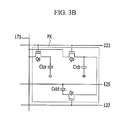
- FIG. 3B is an equivalent circuit diagram of another exemplary embodiment of one pixel of an LCD according to the invention.
- FIG. 3C is an equivalent circuit diagram of an exemplary embodiment of one pixel of an LCD according to the invention.
- FIG. 4A is a view showing a process for providing a pretilt to liquid crystal molecules by using prepolymers that are polymerized by light such as ultraviolet (“UV”) rays.
- UV ultraviolet
- FIG. 4B is a graph showing an experimental example of a transmittance change of an LCD according to the invention.
- FIGS. 5 to 7 are electron microscope photographs showing an experimental example of a transmittance change of an LCD according to the invention.
- FIG. 8 is an electron microscope photograph showing an experimental example of a transmittance change of an LCD according to the invention.
- FIG. 9 is a plan view of another exemplary embodiment of an LCD according to the invention.
- FIG. 10 is a cross-sectional view of the LCD of FIG. 9 taken along line X-X.
- FIG. 11 is a plan view of a pixel electrode of the LCD of FIG. 9 .
- FIG. 12 is a plan view of another exemplary embodiment of an LCD according to the invention.
- FIG. 13 is a cross-sectional view of the LCD of FIG. 12 taken along line XIII-XIII.
- FIG. 14 is a plan view of a pixel electrode of the LCD of FIG. 13 .
- FIG. 15 is a plan view of to another exemplary embodiment of an LCD according the invention.
- FIG. 16 is a cross-sectional view of the LCD of FIG. 15 taken along line XVI-XVI.
- FIG. 17 is a plan view of a pixel electrode of the LCD of FIG. 15 .
- FIG. 18 is a plan view of another exemplary embodiment of an LCD according to the invention.
- FIG. 19 is a cross-sectional view of the LCD of FIG. 18 taken along line XIX-XIX.
- FIG. 20 is a plan view of a pixel electrode of the LCD of FIG. 18 .
- FIG. 21 is an electron microscope photograph showing an experimental example of a transmittance change of an LCD according to the invention.
- FIG. 22 is an electron microscope photograph showing an experimental example of a transmittance change of an LCD according to the invention.
- FIG. 23 is an electron microscope photograph showing an experimental example of a transmittance change of an LCD according to the invention.
- first,” “second,” “third” etc. may be used herein to describe various elements, components, regions, layers and/or sections, these elements, components, regions, layers and/or sections should not be limited by these terms. These terms are only used to distinguish one element, component, region, layer or section from another element, component, region, layer or section. Thus, “a first element,” “component,” “region,” “layer” or “section” discussed below could be termed a second element, component, region, layer or section without departing from the teachings herein.
- relative terms such as “lower” or “bottom” and “upper” or “top,” may be used herein to describe one element's relationship to another element as illustrated in the Figures. It will be understood that relative terms are intended to encompass different orientations of the device in addition to the orientation depicted in the Figures. For example, if the device in one of the figures is turned over, elements described as being on the “lower” side of other elements would then be oriented on “upper” sides of the other elements. The exemplary term “lower,” can therefore, encompasses both an orientation of “lower” and “upper,” depending on the particular orientation of the figure.
- “About” or “approximately” as used herein is inclusive of the stated value and means within an acceptable range of deviation for the particular value as determined by one of ordinary skill in the art, considering the measurement in question and the error associated with measurement of the particular quantity (i.e., the limitations of the measurement system). For example, “about” can mean within one or more standard deviations, or within ⁇ 30%, 20%, 10%, 5% of the stated value.
- Exemplary embodiments are described herein with reference to cross section illustrations that are schematic illustrations of idealized embodiments. As such, variations from the shapes of the illustrations as a result, for example, of manufacturing techniques and/or tolerances, are to be expected. Thus, embodiments described herein should not be construed as limited to the particular shapes of regions as illustrated herein but are to include deviations in shapes that result, for example, from manufacturing. For example, a region illustrated or described as flat may, typically, have rough and/or nonlinear features. Moreover, sharp angles that are illustrated may be rounded. Thus, the regions illustrated in the figures are schematic in nature and their shapes are not intended to illustrate the precise shape of a region and are not intended to limit the scope of the present claims.
- FIG. 1 is a plan view of an LCD according to an exemplary embodiment of the invention
- FIG. 2 is a cross-sectional view of the LCD of FIG. 1 taken along line II-II.
- an LCD according to the exemplary embodiment includes a lower panel 100 and an upper panel 200 facing each other, and a liquid crystal layer 3 interposed between the two display panels 100 and 200 .
- a gate line 121 , a reference voltage line 131 , and a storage electrode 135 are disposed on a first substrate 110 including transparent glass or plastic.
- the gate line 121 transfers a gate signal and mainly extends in a transverse direction.
- the gate line 121 includes a first gate electrode 124 a , a second gate electrode 124 b , a third gate electrode 124 c , and a wide end (not shown) for connection with other layers or an external driving circuit.
- the reference voltage line 131 may extend in parallel to the gate line 121 and includes an expansion 136 , and the expansion 136 is connected to a third drain electrode 175 c that will be described later.
- the reference voltage line 131 includes the storage electrode 135 enclosing a pixel area.
- a gate insulating layer 140 is disposed on the gate line 121 , the reference voltage line 131 , and the storage electrode 135 .
- a first semiconductor 154 a , a second semiconductor 154 b , and a third semiconductor 154 c that may include amorphous silicon or crystalline silicon are disposed on the gate insulating layer 140 .
- a plurality of ohmic contacts 163 a , 163 b , 163 c , 165 a , and 165 b is disposed on the first semiconductor 154 a , the second semiconductor 154 b , and the third semiconductor 154 c .
- the ohmic contacts may be omitted.
- the second drain electrode 175 b is connected to the third source electrode 173 c.
- the first gate electrode 124 a , the first source electrode 173 a , and the first drain electrode 175 a provide a first thin film transistor (“TFT”) Qa along with the first semiconductor 154 a , and a channel of the TFT is provided in the semiconductor 154 a between the first source electrode 173 a and the first drain electrode 175 a .
- TFT thin film transistor
- the second gate electrode 124 b , the second source electrode 173 b , and the second drain electrode 175 b provide a second TFT Qb along with the second semiconductor 154 b , and a channel of the TFT is provided in the semiconductor 154 b between the second source electrode 173 b and the second drain electrode 175 b
- the third gate electrode 124 c , the third source electrode 173 c , and the third drain electrode 175 c provide a third TFT Qc along with the third semiconductor Qc, and a channel of the TFT is provided in the semiconductor 154 c between the third source electrode 173 c and the third drain electrode 175 c.
- a first passivation layer 180 a that may include an inorganic insulator such as silicon nitride or silicon oxide is disposed on the data conductors 171 , 173 a , 173 b , 173 c , 175 a , 175 b , and 175 c and exposed portions of the semiconductors 154 a , 154 b , and 154 c.
- an inorganic insulator such as silicon nitride or silicon oxide
- a color filter 230 is disposed on the first passivation layer 180 a.
- a light blocking member (not shown) may be disposed on a region where the color filter 230 is not disposed and on a portion of the color filter 230 .
- the light blocking member is referred to as a black matrix and prevents light leakage.
- An overcoat (capping layer) 80 is disposed on the color filter 230 .
- the overcoat 80 prevents peeling of the color filter 230 and the light blocking member, and prevents contamination of the liquid crystal layer 3 by an organic material of the solvent that inflows from the color filter 230 , so that it prevents defects such as afterimages that may occur when an image is driven.
- a pixel electrode 191 including a first subpixel electrode 191 a and a second subpixel electrode 191 b that are separated from the first subpixel electrode 191 a and separated from a connection member 97 are disposed on the overcoat 80 .
- an overall shape of the first subpixel electrode 191 a is a polygon shape such as a hexagon, and the first subpixel electrode 191 a is enclosed by the second subpixel electrode 191 b .
- An overall shape of the second subpixel electrode 191 b is a shape of which four trapezoids are gathered, and is disposed at the edge of the pixel area.
- the first subpixel electrode 191 a includes a crossed-shape stem ( 192 and 193 ) including a transverse stem 192 and a longitudinal stem 193 , and a plurality of first branch electrodes 194 extending from the crossed-shape stem ( 192 and 193 ).
- the first branch electrodes 194 extend in four different directions.
- the first branch electrodes 194 include a plurality of first minute branches obliquely extending from the crossed-shape stem ( 192 and 193 ) in the left-upper direction, a plurality of second minute branches obliquely extending in the right-upper direction, a plurality of third minute branches obliquely extending in the left-lower direction, and a plurality of fourth minute branches obliquely extending in the right-lower direction.
- the second subpixel electrode 191 b includes an outer stem 195 enclosing the edge of the pixel area, and a plurality of second branch electrodes 196 extending from the outer stem 195 .
- the second branch electrodes 196 extend in four different directions.
- the second branch electrodes 196 include a plurality of fifth minute branches obliquely extending in the left-upper direction from the outer stem 195 , a plurality of sixth minute branches obliquely extending in the right-upper direction, a plurality of seventh minute branches obliquely extending in the left-lower direction, and a plurality of eighth minute branches obliquely extending in the right-lower direction.
- An interval between an end of the first subpixel electrode 191 a and an end of the second subpixel electrode 191 b adjacent to each other, that is, a separation interval between the first subpixel electrode 191 a and the second subpixel electrode 191 b may be about 1 micrometers ( ⁇ m) to about 5 ⁇ m.
- a first contact hole 185 a exposing a portion of the first drain electrode 175 a , a second contact hole 185 b exposing a portion of the second drain electrode 175 b and a third contact hole 185 c exposing a portion of the third drain electrode 175 c and a portion of the expansion 136 are defined in the first passivation layer 180 a and the overcoat 80 .
- the connection member 97 is disposed on the third drain electrode 175 c and a portion of the expansion 136 exposed through the third contact hole 185 c to connect the third drain electrode 175 c and the expansion 136 to each other.
- the first subpixel electrode 191 a is physically and electrically connected to the first drain electrode 175 a through the first contact hole 185 a
- the second subpixel electrode 191 b is physically and electrically connected to the second drain electrode 175 b through the second contact hole 185 b.
- the first subpixel electrode 191 a and the second subpixel electrode 191 b receive the data voltage from the first drain electrode 175 a and the second drain electrode 175 b through the first contact hole 185 a and the second contact hole 185 b , respectively.
- a light blocking member 220 and a common electrode 270 are disposed on a second substrate 210 including transparent glass or plastic.
- the light blocking member 220 may be disposed on the lower panel 100
- the color filter 230 may be disposed on the upper panel 200 .
- Alignment layers may be disposed on an inner surface of the display panels 100 and 200 , and the alignment layers may include vertical alignment (“VA”) layers.
- VA vertical alignment
- a polarizer (not shown) may be provided on the outer surface of the two display panels 100 and 200 , and it is preferable that transmissive axes of the two polarizers may be orthogonal to each other and that either transmissive axis of them is parallel to the gate line 121 . However, the polarizer may only be disposed at one outer surface of the two display panels 100 and 200 .
- the liquid crystal layer 3 has negative dielectric anisotropy, and liquid crystal molecules of the liquid crystal layer 3 may be aligned so that long axes thereof are perpendicular with respect to the surface of the two display panels 100 and 200 in a state in which electric field is not generated. Therefore, the incident light does not pass through the crossed polarizers but is blocked in a state in which electric field is not generated.
- At least one of the liquid crystal layer 3 and the alignment layer may include a photoreactive material, in detail, a reactive mesogen, for example.
- FIG. 3A is an equivalent circuit diagram of one pixel of an LCD according to an exemplary embodiment of the invention.
- the first gate electrode 124 a , the second gate electrode 124 b , and the third gate electrode 124 c are applied with the gate-on signal such that the first switching element Qa, the second switching element Qb, and the third switching element Qc are turned on. Accordingly, the data voltage applied to the data line 171 is applied to the first subpixel electrode 191 a and the second subpixel electrode 191 b through the turned-on first switching element Qa and second switching element Qb. At this time, the first subpixel electrode 191 a and the second subpixel electrode 191 b are applied with a voltage of the same magnitude.
- the voltage applied to the second subpixel electrode 191 b is divided through the third switching element Qc connected in parallel to the second switching element Qb. Accordingly, the voltage applied to the second subpixel electrode 191 b is lower than the voltage applied to the first subpixel electrode 191 a.
- charge voltages of a first liquid crystal capacitor provided between the first subpixel electrode 191 a and the common electrode 270 and a second liquid crystal capacitor provided between the second subpixel electrode 191 b and the common electrode 270 represent different gamma curves, and a gamma curve of one pixel voltage becomes a combination curved line thereof.
- the combination gamma curve at the front is to be identical to a reference gamma curve at the front that is determined to be most appropriate, and the combination gamma curve at the side of the display is to be closest to the reference gamma curve at the front. As described above, the side visibility is improved by converting the image data.
- the separation interval between the first subpixel electrode 191 a and the second subpixel electrode 191 b may be about 1 ⁇ m to about 5 ⁇ m.
- a ratio of the voltage applied to the second subpixel electrode 191 b to the voltage applied to the first subpixel electrode 191 a is preferably less than about 0.9.
- a ratio of the voltage applied to the second subpixel electrode 191 b to the voltage applied to the first subpixel electrode 191 a is preferably less than about 0.8.
- a ratio of the voltage applied to the second subpixel electrode 191 b to the voltage applied to the first subpixel electrode 191 a is preferably less than about 0.7.
- the first subpixel electrode 191 a and the second subpixel electrode 191 b respectively have an approximate quadrangular shape and are disposed up and down to be separated from each other.
- the first subpixel electrode 191 a and the second subpixel electrode 191 b are respectively provided to have a crossed-shape stem and a plurality of branch electrodes extending from the crossed-shape stem. Therefore, in a region between the first subpixel electrode 191 a and the second subpixel electrode 191 b and each crossed-shape stem region of the first subpixel electrode 191 a and the second subpixel electrode 191 b , the transmittance of the LCD is deteriorated.
- the overall shape of the first subpixel electrode 191 a is the polygon such as the hexagon
- the first subpixel electrode 191 a is enclosed by the second subpixel electrode 191 b
- the overall shape of the second subpixel electrode 191 b is the shape of which four trapezoids are gathered, and is disposed at the edge of the pixel area.
- the first subpixel electrode 191 a includes the crossed-shape stem ( 192 and 193 ) including the transverse stem 192 and the longitudinal stem 193 and a plurality of first branch electrodes 194 extending from the crossed-shape stem ( 192 and 193 ), but the second subpixel electrode 191 b includes the outer stem 195 provided along with the outer edge of the pixel area and a plurality of second branch electrodes 196 extending from the outer stem 195 .
- the separation interval between the first subpixel electrode 191 a and the second subpixel electrode 191 b may be relatively narrow, the stem of the second subpixel electrode 191 b is provided at a center of the pixel area, and the second subpixel electrode 191 b includes the outer stem 195 provided according to the outer edge of the pixel area, thereby preventing the transmittance deterioration generated near the crossed-shape stem.
- a portion of the longitudinal stem 193 of the first subpixel electrode 191 a is disposed between the second branch electrodes 196 of the second subpixel electrode 191 b .
- an electric field is generated between the portion of the longitudinal stem 193 of the first subpixel electrode 191 a and the second branch electrodes 196 of the second subpixel electrode 191 b adjacent to each other.
- the liquid crystal molecules disposed near the portion of the longitudinal stem 193 of the first subpixel electrode 191 a are inclined in the direction almost parallel to the direction that the second branch electrodes 196 of the second subpixel electrode 191 b extend. Therefore, the transmittance deterioration generated near the portion of the longitudinal stem 193 of the first subpixel electrode 191 a may be prevented.
- the transmittance deterioration of the LCD may be prevented.
- the second subpixel electrode 191 b applied with the relatively low voltage encloses the first subpixel electrode 191 a applied with the relatively high voltage and the second subpixel electrode 191 b is disposed at the outer edge of the pixel area, thereby reducing unnecessary parasitic capacitance that may be generated by overlapping of the data line 171 and the pixel electrode 191 .
- the parasitic capacitance is proportional to the voltage magnitude of two overlapping electrodes, the parasitic capacitance generated when the first subpixel electrode 191 a applied with the relatively high voltage and the data line 171 overlap each other is smaller than the parasitic capacitance generated when the second subpixel electrode 191 b applied with the relatively low voltage and the data line 171 overlap each other.
- the unnecessary parasitic capacitance that may be generated by the overlapping of the data line 171 and the pixel electrode 191 may be reduced. Since the unnecessary parasitic capacitance may be reduced, the size of the second subpixel electrode 191 b may be relatively increased, and as a result, the transmittance of the LCD may be increased.
- the output terminal of the second switching element Qb connected to the second subpixel electrode 191 b providing the second liquid crystal capacitor Clcb and the third switching element Qc connected to the divided voltage reference voltage line 131 are included.
- the output terminal of the second switching element Qb connected to the second subpixel electrode 191 b providing the second liquid crystal capacitor Clcb and the third switching element Qc connected to a step-down capacitor may be included. This will be described with reference to FIG. 3B .
- the LCD may include the output terminal of the second switching element Qb connected to the second subpixel electrode 191 b providing the second liquid crystal capacitor Clcb and the third switching element Qc connected to the step-down capacitor Cstd.
- the third switching element Qc may be connected to a step-down gate line 123 different from the first switching element Qa and the second switching element Qb, and after the gate line 121 is applied with the gate-on signal such that the first switching element Qa and the second switching element Qb are turned on then turned off, the step-down gate line 123 is applied with the gate-on signal such that the third switching element Qc may be turned on.
- the charge is moved from the second subpixel electrode 191 b to the step-down capacitor Cstd through the third switching element Qc.
- the charged voltage of the second liquid crystal capacitor Clcb is decreased and the step-down capacitor Cstd is charged.
- the charged voltage of the second liquid crystal capacitor Clcb is decreased by the capacitance of the step-down capacitor Cstd such that the charge voltage of the second liquid crystal capacitor Clcb is lower than the charge voltage of the first liquid crystal capacitor Clca.
- the difference of the charge voltage may be controlled by the magnitude of the voltage applied to a second reference voltage line 125 connected to the other terminal of the step-down capacitor Cstd.
- the first liquid crystal capacitor Clca in a first pixel area PXa of a pixel PX and the second liquid crystal capacitor Clcb in a second pixel area PXb of the pixel PX are respectively connected to a different first data line 171 a and second data line 171 b to be applied with different data voltages, thereby differentiating the charge voltages of the first liquid crystal capacitor and the second liquid crystal capacitor.
- the charge voltage of the first liquid crystal capacitor Clca and the second liquid crystal capacitor Clcb may be differentiated by various methods.
- FIG. 4A is a view showing a process for providing a pretilt to liquid crystal molecules 31 by using prepolymers that are polymerized by light such as ultraviolet (“UV”) rays.
- UV ultraviolet
- prepolymers 330 such as a monomer, which is hardened through polymerization by light such as UV rays, are inserted between the two display panels 100 and 200 along with the liquid crystal material.
- the prepolymers 330 may be a reactive mesogen that is polymerized by light such as UV rays.
- the first subpixel electrode 191 a and the second subpixel electrode 191 b are applied with voltages of different magnitudes and the common electrode 270 of the upper panel 200 is applied with the common voltage to generate the electric field to the liquid crystal layer 3 between the two display panels 100 and 200 .
- the liquid crystal molecules 31 of the liquid crystal layer 3 are respectively inclined in four directions as the direction parallel to the extending direction of the first branch electrodes 194 of the first subpixel electrode 191 a by the fringe field due to the plurality of first branch electrodes 194 of the first subpixel electrode 191 a and the common electrode 270 , and in four directions as the direction parallel to the extending direction of the second branch electrodes 196 of the second subpixel electrode 191 b by the fringe field due to a plurality of second branch electrodes 196 of the second subpixel electrode 191 b and the common electrode 270 .
- the inclination angles of the liquid crystal molecules 31 corresponding to the first subpixel electrode 191 a and the liquid crystal molecules 31 corresponding to the second subpixel electrode 191 b are different with reference to the first substrate 110 .
- the prepolymers 330 are polymerized to provide a polymer 370 .
- the polymer 370 is provided while contacting the display panels 100 and 200 .
- the alignment direction is determined for the liquid crystal molecules 31 to have the pretilt in the length direction of the minute branches by the polymer 370 . Accordingly, the liquid crystal molecules 310 are arranged with the pretilts of four different directions under non-application of the voltage to the electrodes 191 and 270 .
- FIG. 4B is a graph showing a transmittance change in terms of percentage (%) depending on a grayscale in terms of voltage (V) of an LCD according to an experimental example of the invention.
- an area ratio of the first subpixel electrode 191 a and the second subpixel electrode 191 b is about 1:1.5, and in the method of initially aligning the liquid crystal molecules 31 to have the pretilt, while controlling the voltages applied to the first subpixel electrode 191 a and the second subpixel electrode 191 b , the transmittance for each gray at the side of the LCD is measured and is compared with the transmittance for each gray at the front of the LCD.
- a first case B 1 in which the voltage of the first subpixel electrode 191 a and the voltage of the second subpixel electrode 191 b are almost the same at about 9.5 volts (V)
- a second case B 2 in which the voltage of the first subpixel electrode 191 a is about 14.5 V and the voltage of the second subpixel electrode 191 b is about 9.5 V
- a third case B 3 in which the voltage of the first subpixel electrode 191 a is about 12 V and the voltage of the second subpixel electrode 191 b is about 9.5 V
- A represents the transmittance result for each gray in the front of the LCD.
- the difference of the transmittance for each gray is large in the front, but in the second and third cases B 2 and B 3 in which the voltage difference exists between the first subpixel electrode 191 a and the second subpixel electrode 191 b on the initial alignment compared with the first case B 1 , the difference between the transmittance for each gray at the front of the LCD and the transmittance for each gray at the side is decreased.
- the low gray for example, in the region of grays from about 8 to 40, compared with the first case B 1 , in the second case B 2 and the third case B 3 , the difference between the transmittance for each gray at the front of the LCD and the transmittance for each gray at the side is largely reduced.
- FIGS. 5 to 7 are electron microscope photographs showing a transmittance change of an LCD according to an experimental example of the invention.
- the separation distance between the first subpixel electrode 191 a and the second subpixel electrode 191 b is about 3.0 ⁇ m
- a ratio of the voltage of the second subpixel electrode 191 b to the voltage of the first subpixel electrode 191 a is respectively set as about 0.7, about 0.8, and about 0.9
- a transmittance result of the LCD is shown in FIG. 5 .
- (a) is a case that the ratio of the voltage of the second subpixel electrode 191 b to the voltage of the first subpixel electrode 191 a is about 0.7
- (b) is a case that the ratio of the voltage of the second subpixel electrode 191 b to the voltage of the first subpixel electrode 191 a is about 0.8
- (c) is a case that the ratio of the voltage of the second subpixel electrode 191 b to the voltage of the first subpixel electrode 191 a is about 0.9.
- the separation distance between the first subpixel electrode 191 a and the second subpixel electrode 191 b is about 4.0 ⁇ m
- a ratio of the voltage of the second subpixel electrode 191 b to the voltage of the first subpixel electrode 191 a is respectively set as about 0.7, about 0.8, and about 0.9
- a transmittance result of the LCD is shown in FIG. 6 .
- (a) is a case that the ratio of the voltage of the second subpixel electrode 191 b to the voltage of the first subpixel electrode 191 a is about 0.7
- (b) is a case that the ratio of the voltage of the second subpixel electrode 191 b to the voltage of the first subpixel electrode 191 a is about 0.8
- (c) is a case that the ratio of the voltage of the second subpixel electrode 191 b to the voltage of the first subpixel electrode 191 a is about 0.9.
- the separation distance between the first subpixel electrode 191 a and the second subpixel electrode 191 b is about 5.0 ⁇ m
- a ratio of the voltage of the second subpixel electrode 191 b to the voltage of the first subpixel electrode 191 a is respectively set as about 0.7, about 0.8, and about 0.9
- a transmittance result of the LCD is shown in FIG. 7 .
- (a) is a case that the ratio of the voltage of the second subpixel electrode 191 b to the voltage of the first subpixel electrode 191 a is about 0.7
- (b) is a case that the ratio of the voltage of the second subpixel electrode 191 b to the voltage of the first subpixel electrode 191 a is about 0.8
- (c) is a case that the ratio of the voltage of the second subpixel electrode 191 b to the voltage of the first subpixel electrode 191 a is about 0.9.
- the separation distance between the first subpixel electrode 191 a and the second subpixel electrode 191 b is about 3.0 ⁇ m
- the ratio of the voltage of the second subpixel electrode 191 b to the voltage of the first subpixel electrode 191 a is less than about 0.9, it is confirmed that the transmittance is not deteriorated on the whole pixel area of the LCD.
- the separation distance between the first subpixel electrode 191 a and the second subpixel electrode 191 b is about 4.0 ⁇ m
- the ratio of the voltage of the second subpixel electrode 191 b to the voltage of the first subpixel electrode 191 a is less than about 0.8
- the transmittance is not deteriorated on the whole pixel area of the LCD
- the ratio of the voltage of the second subpixel electrode 191 b to the voltage of the first subpixel electrode 191 a is larger than about 0.8
- irregular movement of the liquid crystal molecules is generated in the region of the second subpixel electrode 191 b such that the region where the transmittance is deteriorated is generated.
- the separation distance between the first subpixel electrode 191 a and the second subpixel electrode 191 b is about 5.0 ⁇ m
- the ratio of the voltage of the second subpixel electrode 191 b to the voltage of the first subpixel electrode 191 a is less than about 0.7
- the transmittance is not deteriorated on the whole pixel area of the LCD
- the ratio of the voltage of the second subpixel electrode 191 b to the voltage of the first subpixel electrode 191 a is larger than about 0.7
- an irregular movement of the liquid crystal molecule is generated in the region like the domain boundary of the second subpixel electrode 191 b such that the region where the transmittance is deteriorated is generated.
- FIG. 8 is an electron microscope photograph showing a transmittance change of an LCD according to an experimental example of the invention.
- the transmittance change of one pixel is measured while changing the gray of the LCD.
- (a) represents the transmittance result of a 32 gray
- (b) represents the transmittance result of a 96 gray
- (c) represents the transmittance result of a 128 gray
- (d) represents the transmittance result of a 256 gray.
- the transmittance deterioration is not generated in the boundary region between the first subpixel electrode 191 a and the second subpixel electrode 191 b , and the transmittance deterioration is small near the portion of the longitudinal stem 193 among the crossed-shape stem ( 192 and 193 ) of the first subpixel electrode 191 a.
- FIG. 9 is a plan view of an LCD according to another exemplary embodiment of the invention
- FIG. 10 is a cross-sectional view of the LCD of FIG. 9 taken along line X-X
- FIG. 11 is a plan view of a pixel electrode of the LCD of FIG. 9 .
- the LCD according to the exemplary embodiment is similar to the LCD according to the exemplary embodiment described with reference to FIGS. 1 and 2 .
- the LCD according to the exemplary embodiment includes a lower panel 100 and an upper panel 200 facing each other, and a liquid crystal layer 3 interposed between the two display panels 100 and 200 .
- a gate line 121 , a reference voltage line 131 , and a storage electrode 135 are disposed on a first substrate 110 .
- the gate line 121 includes a first gate electrode 124 a , a second gate electrode 124 b , a third gate electrode 124 c , and a wide end (not shown) for connection with other layers or an external driving circuit
- the reference voltage line 131 includes an expansion 136 and a storage electrode 135 .
- a gate insulating layer 140 is disposed on the gate line 121 , the reference voltage line 131 , and the storage electrode 135 .
- a first semiconductor 154 a , a second semiconductor 154 b , and a third semiconductor 154 c are disposed on the gate insulating layer 140 .
- a plurality of ohmic contacts 163 a , 163 b , 163 c , 165 a , and 165 b is disposed on the first semiconductor 154 a , the second semiconductor 154 b , and the third semiconductor 154 c.
- the second drain electrode 175 b is connected to the third source electrode 173 c.
- the first gate electrode 124 a , the first source electrode 173 a , and the first drain electrode 175 a provide a first TFT Qa along with the first semiconductor 154 a , and a channel of the TFT is provided in the semiconductor 154 a between the first source electrode 173 a and the first drain electrode 175 a .
- the second gate electrode 124 b , the second source electrode 173 b , and the second drain electrode 175 b provide a second TFT Qb along with the second semiconductor 154 b , and a channel of the TFT is provided in the semiconductor 154 b between the second source electrode 173 b and the second drain electrode 175 b
- the third gate electrode 124 c , the third source electrode 173 c , and the third drain electrode 175 c provide a third TFT Qc along with the third semiconductor Qc, and a channel of the TFT is provided in the semiconductor 154 c between the third source electrode 173 c and the third drain electrode 175 c.
- a first passivation layer 180 a is disposed on the data conductors 171 , 173 a , 173 b 173 c , 175 a , 175 b , and 175 c and the exposed portion of the semiconductor 154 a , 154 b , and 154 c.
- a color filter 230 is disposed on the first passivation layer 180 a.
- An overcoat (capping layer) 80 is disposed on the color filter 230 .
- a pixel electrode 191 including a first subpixel electrode 191 a and a second subpixel electrode 191 b that are separated from each other and a connection member 97 are disposed on the overcoat 80 .
- the overall shape of the first subpixel electrode 191 a is a polygon shape such as a hexagon, and the first subpixel electrode 191 a is enclosed by the second subpixel electrode 191 b .
- the overall shape of the second subpixel electrode 191 b is the shape of which four trapezoids are gathered, and is disposed at the edge of the pixel area.
- the first subpixel electrode 191 a includes a crossed-shape stem ( 192 and 193 ) including a transverse stem 192 and a longitudinal stem 193 , and a plurality of first branch electrodes 194 extending from the crossed-shape stem ( 192 and 193 ).
- a first connection 197 connects two adjacent first branch electrodes 194 .
- the first branch electrodes 194 extend in four different directions.
- the first branch electrodes 194 include a plurality of first minute branches obliquely extending from the crossed-shape stem ( 192 and 193 ) in the left-upper direction, a plurality of second minute branches obliquely extending in the right-upper direction, a plurality of third minute branches obliquely extending in the left-lower direction, and a plurality of fourth minute branches obliquely extending in the right-lower direction.
- the second subpixel electrode 191 b includes a plurality of second branch electrodes 196 , a plurality of second connections 195 a , and a plurality of third connections 195 b .
- the second branch electrodes 196 extend in four different directions.
- the second branch electrodes 196 include a plurality of fifth minute branches obliquely extending in the left-upper direction from the plurality of second connections 195 a and the plurality of third connections 195 b , a plurality of sixth minute branches obliquely extending in the right-upper direction, a plurality of seventh minute branches obliquely extending in the left-lower direction, and a plurality of eighth minute branches obliquely extending in the right-lower direction.
- An interval between an end of the first subpixel electrode 191 a and an end of the second subpixel electrode 191 b adjacent to each other, that is, a separation interval between the first subpixel electrode 191 a and the second subpixel electrode 191 b , may be about 1 ⁇ m to about 5 ⁇ m.
- a first contact hole 185 a exposing a portion of the first drain electrode 175 a , a second contact hole 185 b exposing a portion of the second drain electrode 175 b , and a third contact hole 185 c exposing a portion of the third drain electrode 175 c and a portion of the expansion 136 are defined in the first passivation layer 180 a and the overcoat 80 .
- the connection member 97 is disposed on the third drain electrode 175 c and a portion of the expansion 136 exposed through the third contact hole 185 c to connect the third drain electrode 175 c and the expansion 136 to each other.
- the first subpixel electrode 191 a is physically and electrically connected to the first drain electrode 175 a through the first contact hole 185 a
- the second subpixel electrode 191 b is physically and electrically connected to the second drain electrode 175 b through the second contact hole 185 b.
- the first subpixel electrode 191 a and the second subpixel electrode 191 b receive the data voltage from the first drain electrode 175 a and the second drain electrode 175 b through the first contact hole 185 a and the second contact hole 185 b.
- a light blocking member 220 and a common electrode 270 are disposed on a second substrate 210 including transparent glass or plastic.
- Alignment layers may be disposed on an inner surface of the display panels 100 and 200 , and the alignment layers may include VA layers.
- the liquid crystal layer 3 has negative dielectric anisotropy, and liquid crystal molecules of the liquid crystal layer 3 may be aligned so that long axes thereof are perpendicular with respect to the surface of the two display panels 100 and 200 in a state in which electric field is not generated. Therefore, the incident light does not pass through the crossed polarizers but is blocked in a state in which electric field is not generated.
- At least one of the liquid crystal layer 3 and the alignment layer may include a photoreactive material, and in detail, a reactive mesogen, for example.
- the shape of the pixel electrode 191 is different from the exemplary embodiment shown in FIGS. 1 and 2 . This will be described with reference to FIG. 11 .
- the pixel electrode 191 of the LCD includes the first subpixel electrode 191 a and the second subpixel electrode 191 b.
- the overall shape of the first subpixel electrode 191 a is the polygon shape such as a hexagon, the first subpixel electrode 191 a is enclosed by the second subpixel electrode 191 b , and the overall shape of the second subpixel electrode 191 b is the shape of which four trapezoids are gathered, and is disposed at the edge of the pixel area.
- the first subpixel electrode 191 a includes the crossed-shape stem ( 192 and 193 ) including the transverse stem 192 and the longitudinal stem 193 , the plurality of first branch electrodes 194 extending from the crossed-shape stem ( 192 and 193 ), and the plurality of first connections 197 .
- Each first connection 197 connects two adjacent first branch electrodes 194 .
- the first branch electrodes 194 extend in four different directions.
- the first branch electrodes 194 include a plurality of first minute branches obliquely extending from the crossed-shape stem ( 192 and 193 ) in the left-upper direction, a plurality of second minute branches obliquely extending in the right-upper direction, a plurality of third minute branches obliquely extending in the left-lower direction, and a plurality of fourth minute branches obliquely extending in the right-lower direction.
- the second subpixel electrode 191 b includes the plurality of second branch electrodes 196 , the plurality of second connections 195 a , and the plurality of third connection 195 b .
- Each second connection 195 a connects two adjacent second branch electrodes 196 and is disposed at the edge of the pixel area
- each third connection 195 b connects two adjacent second branch electrodes 196 and is disposed at the edge of the second subpixel electrode 191 b adjacent to the first subpixel electrode 191 a .
- the plurality of second connections 195 a and the plurality of third connections 195 b are alternately provided.
- the second branch electrodes 196 extend in four different directions.
- the second branch electrodes 196 include a plurality of fifth minute branches obliquely extending in the left-upper direction from the outer stem 195 , a plurality of sixth minute branches obliquely extending in the right-upper direction, a plurality of seventh minute branches obliquely extending in the left-lower direction, and a plurality of eighth minute branches obliquely extending in the right-lower direction.
- a plurality of first connections 197 of the first subpixel electrode 191 a is disposed at the edge of the first subpixel electrode 191 a adjacent to the second subpixel electrode 191 a , and a plurality of first connections 197 is disposed to be adjacent to a plurality of third connections 195 b of the second subpixel electrode 191 b.
- FIG. 12 is a plan view of an LCD according to another exemplary embodiment of the invention
- FIG. 13 is a cross-sectional view of the LCD of FIG. 12 taken along line XIII-XIII
- FIG. 14 is a plan view of a pixel electrode of the LCD of FIG. 13 .
- the LCD according to the exemplary embodiment is similar to the LCD according to the exemplary embodiment described with reference to FIGS. 1 and 2 .
- the LCD according to the exemplary embodiment includes a lower panel 100 and an upper panel 200 facing each other, and a liquid crystal layer 3 interposed between the two display panels 100 and 200 .
- a gate line 121 , a reference voltage line 131 , and a storage electrode 135 are disposed on a first substrate 110 .
- the gate line 121 includes a first gate electrode 124 a , a second gate electrode 124 b , a third gate electrode 124 c , and a wide end (not shown) for connection with other layers or an external driving circuit, and the reference voltage line 131 includes an expansion 136 and the storage electrode 135 .
- a gate insulating layer 140 is disposed on the gate line 121 , the reference voltage line 131 , and the storage electrode 135 .
- a first semiconductor 154 a , a second semiconductor 154 b , and a third semiconductor 154 c are disposed on the gate insulating layer 140 .
- a plurality of ohmic contacts 163 a , 163 b , 163 c , 165 a , and 165 b is disposed on the first semiconductor 154 a , the second semiconductor 154 b , and the third semiconductor 154 c.
- the second drain electrode 175 b is connected to the third source electrode 173 c.
- the first gate electrode 124 a , the first source electrode 173 a , and the first drain electrode 175 a provide a first TFT Qa along with the first semiconductor 154 a , and a channel of the TFT is provided in the semiconductor 154 a between the first source electrode 173 a and the first drain electrode 175 a .
- the second gate electrode 124 b , the second source electrode 173 b , and the second drain electrode 175 b provide a second TFT Qb along with the second semiconductor 154 b , and a channel of the TFT is provided in the semiconductor 154 b between the second source electrode 173 b and the second drain electrode 175 b
- the third gate electrode 124 c , the third source electrode 173 c , and the third drain electrode 175 c provide a third TFT Qc along with the third semiconductor Qc, and a channel of the TFT is provided in the semiconductor 154 c between the third source electrode 173 c and the third drain electrode 175 c.
- a first passivation layer 180 a is disposed on the data conductors 171 , 173 a , 173 b 173 c , 175 a , 175 b , and 175 c and the exposed portion of the semiconductors 154 a , 154 b , and 154 c.
- a color filter 230 is disposed on the first passivation layer 180 a.
- An overcoat (capping layer) 80 is disposed on the color filter 230 .
- a pixel electrode 191 including a first subpixel electrode 191 a and a second subpixel electrode 191 b that are separated from each other and a connection member 97 are disposed on the overcoat 80 .
- the overall shape of the first subpixel electrode 191 a is a polygon shape such as a hexagon, and the first subpixel electrode 191 a is enclosed by the second subpixel electrode 191 b .
- the overall shape of the second subpixel electrode 191 b is the shape of which four trapezoids are gathered, and is disposed at the edge of the pixel area.
- the first subpixel electrode 191 a includes a crossed-shape stem ( 192 and 193 ) including a transverse stem 192 and a longitudinal stem 193 , and a plurality of first branch electrodes 194 extending from the crossed-shape stem ( 192 and 193 ).
- the first branch electrodes 194 extend in four different directions.
- the first branch electrodes 194 include a plurality of first minute branches obliquely extending from the crossed-shape stem ( 192 and 193 ) in the left-upper direction, a plurality of second minute branches obliquely extending in the right-upper direction, a plurality of third minute branches obliquely extending in the left-lower direction, and a plurality of fourth minute branches obliquely extending in the right-lower direction.
- the second subpixel electrode 191 b includes a plurality of second branch electrodes 196 , a plurality of second connections 195 a , and a plurality of third connections 195 b .
- the second branch electrodes 196 extend in four different directions.
- the second branch electrodes 196 include a plurality of fifth minute branches obliquely extending in the left-upper direction from the plurality of second connections 195 a and a plurality of third connections 195 b , a plurality of sixth minute branches obliquely extending in the right-upper direction, a plurality of seventh minute branches obliquely extending in the left-lower direction, and a plurality of eighth minute branches obliquely extending in the right-lower direction.
- An interval between an end of the first subpixel electrode 191 a and an end of the second subpixel electrode 191 b adjacent to each other, that is, a separation interval between the first subpixel electrode 191 a and the second subpixel electrode 191 b , may be about 1 ⁇ m to about 5 ⁇ m.
- a first contact hole 185 a exposing a portion of the first drain electrode 175 a , a second contact hole 185 b exposing a portion of the second drain electrode 175 b , and a third contact hole 185 c exposing a portion of the third drain electrode 175 c and a portion of the expansion 136 are defined in the first passivation layer 180 a and the overcoat 80 .
- the connection member 97 is disposed on the third drain electrode 175 c and a portion of the expansion 136 exposed through the third contact hole 185 c to connect the third drain electrode 175 c and the expansion 136 to each other.
- the first subpixel electrode 191 a is physically and electrically connected to the first drain electrode 175 a through the first contact hole 185 a
- the second subpixel electrode 191 b is physically and electrically connected to the second drain electrode 175 b through the second contact hole 185 b.
- the first subpixel electrode 191 a and the second subpixel electrode 191 b receive the data voltage from the first drain electrode 175 a and the second drain electrode 175 b through the first contact hole 185 a and the second contact hole 185 b.
- a light blocking member 220 and a common electrode 270 are disposed on a second substrate 210 including transparent glass or plastic.
- Alignment layers may be disposed on an inner surface of the display panels 100 and 200 , and the alignment layers may include VA layers.
- the liquid crystal layer 3 has negative dielectric anisotropy, and liquid crystal molecules of the liquid crystal layer 3 may be aligned so that long axes thereof are perpendicular with respect to the surface of the two display panels 100 and 200 in a state in which electric field is not generated. Therefore, the incident light does not pass through the crossed polarizers but is blocked in a state in which electric field is not generated.
- At least one of the liquid crystal layer 3 and the alignment layer may include a photoreactive material, and in detail, a reactive mesogen, for example.
- the shape of the pixel electrode 191 is different from the exemplary embodiment shown in FIGS. 1 and 2 . This will be described with reference to FIG. 14 .
- the pixel electrode 191 of the LCD includes the first subpixel electrode 191 a and the second subpixel electrode 191 b.
- the overall shape of the first subpixel electrode 191 a is the polygon shape such as a hexagon, the first subpixel electrode 191 a is enclosed by the second subpixel electrode 191 b , and the overall shape of the second subpixel electrode 191 b is the shape of which four trapezoids are gathered, and is disposed at the edge of the pixel area.
- the first subpixel electrode 191 a includes the crossed-shape stem ( 192 and 193 ) including the transverse stem 192 and the longitudinal stem 193 and a plurality of first branch electrodes 194 extending from the crossed-shape stem ( 192 and 193 ).
- the first branch electrodes 194 extend in four different directions.
- the first branch electrodes 194 include a plurality of first minute branches obliquely extending from the crossed-shape stem ( 192 and 193 ) in the left-upper direction, a plurality of second minute branches obliquely extending in the right-upper direction, a plurality of third minute branches obliquely extending in the left-lower direction, and a plurality of fourth minute branches obliquely extending in the right-lower direction.
- the second subpixel electrode 191 b includes a plurality of second branch electrodes 196 , a plurality of second connections 195 a , and a plurality of third connection 195 b .
- the second connection 195 a connects two adjacent second branch electrodes 196 and is disposed at the edge of the pixel area
- the third connection 195 b connects two adjacent second branch electrodes 196 and is disposed at the edge of the second subpixel electrode 191 b adjacent to the first subpixel electrode 191 a .
- the plurality of second connections 195 a and the plurality of third connections 195 b are alternately provided.
- the second branch electrodes 196 extend in four different directions.
- the second branch electrodes 196 include a plurality of fifth minute branches obliquely extending in the left-upper direction from the outer stem 195 , a plurality of sixth minute branches obliquely extending in the right-upper direction, a plurality of seventh minute branches obliquely extending in the left-lower direction, and a plurality of eighth minute branches obliquely extending in the right-lower direction.
- FIG. 15 is a plan view of an LCD according to another exemplary embodiment of the invention
- FIG. 16 is a cross-sectional view of the LCD of FIG. 15 taken along line XVI-XVI
- FIG. 17 is a plan view of a pixel electrode of the LCD of FIG. 15 .
- the LCD according to the exemplary embodiment is similar to the LCD according to the exemplary embodiment described with reference to FIGS. 1 and 2 .
- the LCD according to the exemplary embodiment includes a lower panel 100 and an upper panel 200 facing each other, and a liquid crystal layer 3 interposed between the two display panels 100 and 200 .
- a gate line 121 , a reference voltage line 131 , and a storage electrode 135 are disposed on a first substrate 110 .
- the gate line 121 includes a first gate electrode 124 a , a second gate electrode 124 b , a third gate electrode 124 c , and a wide end (not shown) for connection with other layers or an external driving circuit, and the reference voltage line 131 includes an expansion 136 and the storage electrode 135 .
- a gate insulating layer 140 is disposed on the gate line 121 , the reference voltage line 131 , and the storage electrode 135 .
- a first semiconductor 154 a , a second semiconductor 154 b , and a third semiconductor 154 c are disposed on the gate insulating layer 140 .
- a plurality of ohmic contacts 163 a , 163 b , 163 c , 165 a , and 165 b is disposed on the first semiconductor 154 a , the second semiconductor 154 b , and the third semiconductor 154 c.
- the second drain electrode 175 b is connected to the third source electrode 173 c.
- the first gate electrode 124 a , the first source electrode 173 a , and the first drain electrode 175 a provide a first TFT Qa along with the first semiconductor 154 a , and a channel of the TFT is provided in the semiconductor 154 a between the first source electrode 173 a and the first drain electrode 175 a .
- the second gate electrode 124 b , the second source electrode 173 b , and the second drain electrode 175 b provide a second TFT Qb along with the second semiconductor 154 b , and a channel of the TFT is provided in the semiconductor 154 b between the second source electrode 173 b and the second drain electrode 175 b
- the third gate electrode 124 c , the third source electrode 173 c , and the third drain electrode 175 c provide a third TFT Qc along with the third semiconductor Qc, and a channel of the TFT is provided in the semiconductor 154 c between the third source electrode 173 c and the third drain electrode 175 c.
- a first passivation layer 180 a is disposed on the data conductors 171 , 173 a , 173 b 173 c , 175 a , 175 b , and 175 c and the exposed portion of the semiconductor 154 a , 154 b , and 154 c.
- a color filter 230 is disposed on the first passivation layer 180 a.
- An overcoat (capping layer) 80 is disposed on the color filter 230 .
- a pixel electrode 191 including a first subpixel electrode 191 a and a second subpixel electrode 191 b that are separated from each other and a connection member 97 are disposed on the overcoat 80 .
- the overall shape of the first subpixel electrode 191 a is a polygon shape such as a hexagon, and the first subpixel electrode 191 a is enclosed by the second subpixel electrode 191 b .
- the overall shape of the second subpixel electrode 191 b is the shape of which four trapezoids are gathered, and is disposed at the edge of the pixel area.
- the first subpixel electrode 191 a includes a crossed-shape stem ( 192 and 193 ) including a transverse stem 192 and a longitudinal stem 193 and a plurality of first branch electrodes 194 extending from the crossed-shape stem ( 192 and 193 ).
- the first branch electrodes 194 extend in four different directions.
- the first branch electrodes 194 include a plurality of first minute branches obliquely extending from the crossed-shape stem ( 192 and 193 ) in the left-upper direction, a plurality of second minute branches obliquely extending in the right-upper direction, a plurality of third minute branches obliquely extending in the left-lower direction, and a plurality of fourth minute branches obliquely extending in the right-lower direction.
- the second subpixel electrode 191 b includes an outer stem 195 a disposed at the edge of the pixel area, a first stem 198 a disposed at the edge adjacent to the first subpixel electrode 191 a , and a plurality of second branch electrodes 196 extending from the outer stem 195 a and the first stem 198 a .
- the second branch electrodes 196 extend in four different directions.
- the second branch electrodes 196 include a plurality of fifth minute branches obliquely extending in the left-upper direction from the outer stem 195 a , a plurality of sixth minute branches obliquely extending in the right-upper direction, a plurality of seventh minute branches obliquely extending in the left-lower direction, and a plurality of eighth minute branches obliquely extending in the right-lower direction.
- An interval between an end of the first subpixel electrode 191 a and an end of the second subpixel electrode 191 b adjacent to each other, that is, a separation interval between the first subpixel electrode 191 a and the second subpixel electrode 191 b , may be about 1 ⁇ m to about 5 ⁇ m.
- a first contact hole 185 a exposing a portion of the first drain electrode 175 a , a second contact hole 185 b exposing a portion of the second drain electrode 175 b , and a third contact hole 185 c exposing a portion of the third drain electrode 175 c and a portion of the expansion 136 are defined in the first passivation layer 180 a and the overcoat 80 .
- the connection member 97 is disposed on the third drain electrode 175 c and a portion of the expansion 136 exposed through the third contact hole 185 c to connect the third drain electrode 175 c and the expansion 136 to each other.
- the first subpixel electrode 191 a is physically and electrically connected to the first drain electrode 175 a through the first contact hole 185 a
- the second subpixel electrode 191 b is physically and electrically connected to the second drain electrode 175 b through the second contact hole 185 b.
- the first subpixel electrode 191 a and the second subpixel electrode 191 b receive the data voltage from the first drain electrode 175 a and the second drain electrode 175 b through the first contact hole 185 a and the second contact hole 185 b.
- a light blocking member 220 and a common electrode 270 are disposed on a second substrate 210 including transparent glass or plastic.
- Alignment layers may be disposed on an inner surface of the display panels 100 and 200 , and the alignment layers may include VA layers.
- the liquid crystal layer 3 has negative dielectric anisotropy, and liquid crystal molecules of the liquid crystal layer 3 may be aligned so that long axes thereof are perpendicular with respect to the surface of the two display panels 100 and 200 in a state in which there is electric field is not generated. Therefore, the incident light does not pass through the crossed polarizers but is blocked in a state in which electric field is not generated.
- At least one of the liquid crystal layer 3 and the alignment layer may include a photoreactive material, and in detail, a reactive mesogen, for example.
- the shape of the pixel electrode 191 is different from the exemplary embodiment shown in FIGS. 1 and 2 . This will be described with reference to FIG. 17 .
- the pixel electrode 191 of the LCD includes the first subpixel electrode 191 a and the second subpixel electrode 191 b.
- the overall shape of the first subpixel electrode 191 a is the polygon shape such as the hexagon, the first subpixel electrode 191 a is enclosed by the second subpixel electrode 191 b , and the overall shape of the second subpixel electrode 191 b is the shape of which four trapezoids are gathered, and is disposed at the edge of the pixel area.
- the first subpixel electrode 191 a includes the crossed-shape stem ( 192 and 193 ) including the transverse stem 192 and the longitudinal stem 193 , and the plurality of first branch electrodes 194 extending from the crossed-shape stem ( 192 and 193 ).
- the first branch electrodes 194 extend in four different directions.
- the first branch electrodes 194 include a plurality of first minute branches obliquely extending from the crossed-shape stem ( 192 and 193 ) in the left-upper direction, a plurality of second minute branches obliquely extending in the right-upper direction, a plurality of third minute branches obliquely extending in the left-lower direction, and a plurality of fourth minute branches obliquely extending in the right-lower direction.
- the second subpixel electrode 191 b includes an outer stem 195 disposed at the edge of the pixel area, a first stem 198 a disposed at the edge adjacent to the first subpixel electrode 191 a , and a plurality of second branch electrodes 196 extending from the outer stem 195 and the first stem 198 a .
- the second branch electrodes 196 extend in four different directions.
- the second branch electrodes 196 include a plurality of fifth minute branches obliquely extending in the left-upper direction from the outer stem 195 , a plurality of sixth minute branches obliquely extending in the right-upper direction, a plurality of seventh minute branches obliquely extending in the left-lower direction, and a plurality of eighth minute branches obliquely extending in the right-lower direction.
- FIG. 18 is a plan view of an LCD according to another exemplary embodiment of the invention
- FIG. 19 is a cross-sectional view of the LCD of FIG. 18 taken along line XIX-XIX
- FIG. 20 is a plan view of a pixel electrode of the LCD of FIG. 18 .
- the LCD according to the exemplary embodiment is similar to the LCD according to the exemplary embodiment described with reference to FIGS. 1 and 2 .
- the LCD according to the exemplary embodiment includes a lower panel 100 and an upper panel 200 facing each other, and a liquid crystal layer 3 interposed between the two display panels 100 and 200 .
- a gate line 121 , a reference voltage line 131 , and a storage electrode 135 are disposed on a first substrate 110 .
- the gate line 121 includes a first gate electrode 124 a , a second gate electrode 124 b , a third gate electrode 124 c , and a wide end (not shown) for connection with other layers or an external driving circuit, and the reference voltage line 131 includes an expansion 136 and the storage electrode 135 .
- a gate insulating layer 140 is disposed on the gate line 121 , the reference voltage line 131 , and the storage electrode 135 .
- a first semiconductor 154 a , a second semiconductor 154 b , and a third semiconductor 154 c are disposed on the gate insulating layer 140 .
- a plurality of ohmic contacts 163 a , 163 b , 163 c , 165 a , and 165 b is disposed on the first semiconductor 154 a , the second semiconductor 154 b , and the third semiconductor 154 c.
- the second drain electrode 175 b is connected to the third source electrode 173 c.
- the first gate electrode 124 a , the first source electrode 173 a , and the first drain electrode 175 a provide a first TFT Qa along with the first semiconductor 154 a , and a channel of the TFT is provided in the semiconductor 154 a between the first source electrode 173 a and the first drain electrode 175 a .
- the second gate electrode 124 b , the second source electrode 173 b , and the second drain electrode 175 b provide a second TFT Qb along with the second semiconductor 154 b , and a channel of the TFT is provided in the semiconductor 154 b between the second source electrode 173 b and the second drain electrode 175 b
- the third gate electrode 124 c , the third source electrode 173 c , and the third drain electrode 175 c provide a third TFT Qc along with the third semiconductor Qc, and a channel of the TFT is provided in the semiconductor 154 c between the third source electrode 173 c and the third drain electrode 175 c.
- a first passivation layer 180 a is disposed on the data conductors 171 , 173 a , 173 b 173 c , 175 a , 175 b , and 175 c and the exposed portion of the semiconductors 154 a , 154 b , and 154 c.
- a color filter 230 is disposed on the first passivation layer 180 a.
- An overcoat (capping layer) 80 is disposed on the color filter 230 .
- a pixel electrode 191 including a first subpixel electrode 191 a and a second subpixel electrode 191 b that are separated from each other and a connection member 97 are disposed on the overcoat 80 .
- the overall shape of the first subpixel electrode 191 a is a polygon shape such as a hexagon, and the first subpixel electrode 191 a is enclosed by the second subpixel electrode 191 b .
- the overall shape of the second subpixel electrode 191 b is the shape of which four trapezoids are gathered, and is disposed at the edge of the pixel area.
- the first subpixel electrode 191 a includes a crossed-shape stem ( 192 and 193 ) including a transverse stem 192 and a longitudinal stem 193 and a plurality of first branch electrodes 194 extending from the crossed-shape stem ( 192 and 193 ).
- the first subpixel electrode 191 a is disposed at the edge adjacent to the second subpixel electrode 191 b , and includes a second stem 198 b connecting a plurality of first branch electrodes 194 to each other.
- the first branch electrodes 194 extend in four different directions.
- the first branch electrodes 194 include a plurality of first minute branches obliquely extending from the crossed-shape stem ( 192 and 193 ) in the left-upper direction, a plurality of second minute branches obliquely extending in the right-upper direction, a plurality of third minute branches obliquely extending in the left-lower direction, and a plurality of fourth minute branches obliquely extending in the right-lower direction.
- the second subpixel electrode 191 b includes an outer stem 195 a disposed at the edge of the pixel area, a first stem 198 a disposed at the edge adjacent to the first subpixel electrode 191 a , and a plurality of second branch electrodes 196 extending from the outer stem 195 a and the first stem 198 a .
- the second branch electrodes 196 extend in four different directions.
- the second branch electrodes 196 include a plurality of fifth minute branches obliquely extending in the left-upper direction from the outer stem 195 , a plurality of sixth minute branches obliquely extending in the right-upper direction, a plurality of seventh minute branches obliquely extending in the left-lower direction, and a plurality of eighth minute branches obliquely extending in the right-lower direction.
- An interval between an end of the first subpixel electrode 191 a and an end of the second subpixel electrode 191 b adjacent to each other, that is, a separation interval between the first subpixel electrode 191 a and the second subpixel electrode 191 b , may be about 1 ⁇ m to about 5 ⁇ m.
- a first contact hole 185 a exposing a portion of the first drain electrode 175 a , a second contact hole 185 b exposing a portion of the second drain electrode 175 b , and a third contact hole 185 c exposing a portion of the third drain electrode 175 c and a portion of the expansion 136 are defined in the first passivation layer 180 a and the overcoat 80 .
- the connection member 97 is disposed on the third drain electrode 175 c and a portion of the expansion 136 exposed through the third contact hole 185 c to connect the third drain electrode 175 c and the expansion 136 to each other.
- the first subpixel electrode 191 a is physically and electrically connected to the first drain electrode 175 a through the first contact hole 185 a
- the second subpixel electrode 191 b is physically and electrically connected to the second drain electrode 175 b through the second contact hole 185 b.
- the first subpixel electrode 191 a and the second subpixel electrode 191 b receive the data voltage from the first drain electrode 175 a and the second drain electrode 175 b through the first contact hole 185 a and the second contact hole 185 b.
- a light blocking member 220 and a common electrode 270 are disposed on a second substrate 210 including transparent glass or plastic.
- Alignment layers may be disposed on an inner surface of the display panels 100 and 200 , and the alignment layers may include VA layers.
- the liquid crystal layer 3 has negative dielectric anisotropy, and liquid crystal molecules of the liquid crystal layer 3 may be aligned so that long axes thereof are perpendicular with respect to the surface of the two display panels 100 and 200 in a state in which electric field is not generated. Therefore, the incident light does not pass through the crossed polarizers but is blocked in a state in which electric field is not generated.
- At least one of the liquid crystal layer 3 and the alignment layer may include a photoreactive material, and in detail, a reactive mesogen, for example.
- the shape of the pixel electrode 191 is different from the exemplary embodiment shown in FIGS. 1 and 2 . This will be described with reference to FIG. 20 .
- the pixel electrode 191 of the LCD includes the first subpixel electrode 191 a and the second subpixel electrode 191 b.
- the overall shape of the first subpixel electrode 191 a is a polygon shape such as a hexagon, the first subpixel electrode 191 a is enclosed by the second subpixel electrode 191 b , and the overall shape of the second subpixel electrode 191 b is the shape of which four trapezoids are gathered, and is disposed at the edge of the pixel area.
- the first subpixel electrode 191 a includes the crossed-shape stem ( 192 and 193 ) including the transverse stem 192 and the longitudinal stem 193 , and a plurality of first branch electrodes 194 extending from the crossed-shape stem ( 192 and 193 ).
- the first subpixel electrode 191 a is disposed at the edge adjacent to the second subpixel electrode 191 b , and includes a second stem 198 b connecting a plurality of first branch electrodes 194 to each other.
- the first branch electrodes 194 extend in four different directions.
- the first branch electrodes 194 include a plurality of first minute branches obliquely extending from the crossed-shape stem ( 192 and 193 ) in the left-upper direction, a plurality of second minute branches obliquely extending in the right-upper direction, a plurality of third minute branches obliquely extending in the left-lower direction, and a plurality of fourth minute branches obliquely extending in the right-lower direction.
- the second subpixel electrode 191 b includes an outer stem 195 disposed at the edge of the pixel area, a first stem 198 a disposed at the edge adjacent to the first subpixel electrode 191 a , and a plurality of second branch electrodes 196 extending from the outer stem 195 and the first stem 198 a .
- the second branch electrodes 196 extend in four different directions.
- the second branch electrodes 196 include a plurality of fifth minute branches obliquely extending in the left-upper direction from the outer stem 195 , a plurality of sixth minute branches obliquely extending in the right-upper direction, a plurality of seventh minute branches obliquely extending in the left-lower direction, and a plurality of eighth minute branches obliquely extending in the right-lower direction.
- the second stem 198 b of the first subpixel electrode 191 a is disposed to be adjacent to the first stem 198 a of the second subpixel electrode 191 b.
- FIGS. 21 to 23 are electron microscope photographs showing a transmittance change of an LCD according to an experimental example of the invention.
- a plurality of pixels according to the LCD according to the exemplary embodiment shown in FIGS. 1 and 2 are provided, a plurality of pixels according to the LCD according to the exemplary embodiment shown in FIGS. 15 and 17 are provided, and a plurality of pixels according to the LCD according to the exemplary embodiment shown in FIGS. 18 and 20 are provided, and for each case, while controlling the ratio of the voltage applied to the second subpixel electrode 191 b to the voltage applied to the first subpixel electrode 191 a , the transmittance result is measured.
- FIG. 21 shows a result of a case that a plurality of pixels according to the LCD according to the exemplary embodiment shown in FIGS. 1 and 2 are provided
- FIG. 22 shows a result of a case that a plurality of pixels according to the LCD according to the exemplary embodiment shown in FIGS. 15 and 17 are provided
- FIG. 23 shows a result of a case that a plurality of pixels according to the LCD according to the exemplary embodiment shown in FIGS. 18 and 20 are provided.
- FIGS. 21 to 23 (a) shows a case that the magnitude of the voltage applied to the first subpixel electrode 191 a is about 9.5 V and the magnitude of the voltage applied to the second subpixel electrode 191 a is about 5.5 V, (b) shows a case that the magnitude of the voltage applied to the first subpixel electrode 191 a is about 12 V and the magnitude of the voltage applied to the second subpixel electrode 191 a is about 7.6 V, (c) shows a case that the magnitude of the voltage applied to the first subpixel electrode 191 a is about 14.5 V and the magnitude of the voltage applied to the second subpixel electrode 191 a is about 10.8 V, and (d) shows a case that the magnitude of the voltage applied to the first subpixel electrode 191 a is about 17.0 V and the magnitude of the voltage applied to the second subpixel electrode 191 a is about 12.8 V.
- the LCD according to the exemplary embodiments of the invention has high transmittance except for the boundary portion between the first subpixel electrode 191 a and the second subpixel electrode 191 b.
Applications Claiming Priority (2)
| Application Number | Priority Date | Filing Date | Title |
|---|---|---|---|
| KR1020130158709A KR20150071550A (ko) | 2013-12-18 | 2013-12-18 | 액정 표시 장치 |
| KR10-2013-0158709 | 2013-12-18 |
Publications (2)
| Publication Number | Publication Date |
|---|---|
| US20150168789A1 US20150168789A1 (en) | 2015-06-18 |
| US9568785B2 true US9568785B2 (en) | 2017-02-14 |
Family
ID=53368253
Family Applications (1)
| Application Number | Title | Priority Date | Filing Date |
|---|---|---|---|
| US14/541,263 Active 2035-02-20 US9568785B2 (en) | 2013-12-18 | 2014-11-14 | Liquid crystal display |
Country Status (2)
| Country | Link |
|---|---|
| US (1) | US9568785B2 (ko) |
| KR (1) | KR20150071550A (ko) |
Families Citing this family (22)
| Publication number | Priority date | Publication date | Assignee | Title |
|---|---|---|---|---|
| KR102158543B1 (ko) | 2014-04-17 | 2020-09-23 | 삼성디스플레이 주식회사 | 액정 표시 장치 및 그 제조 방법 |
| KR102567648B1 (ko) * | 2016-03-14 | 2023-08-17 | 삼성디스플레이 주식회사 | 액정 표시 장치 |
| USD792878S1 (en) * | 2016-10-28 | 2017-07-25 | Modne Inc. | Case for a cellular phone with a surface pattern |
| USD792877S1 (en) * | 2016-10-28 | 2017-07-25 | Modne Inc. | Case for a cellular phone with a surface pattern |
| KR102345437B1 (ko) * | 2017-06-28 | 2021-12-30 | 삼성디스플레이 주식회사 | 표시 장치 |
| USD841637S1 (en) * | 2017-08-07 | 2019-02-26 | Modne, Inc. | Phone case |
| USD832833S1 (en) * | 2017-08-16 | 2018-11-06 | Modne, Inc. | Phone case |
| USD883971S1 (en) * | 2017-08-16 | 2020-05-12 | Spigen, Inc. | Phone case |
| USD888033S1 (en) * | 2017-08-16 | 2020-06-23 | Spigen, Inc. | Phone case |
| USD831638S1 (en) * | 2017-08-16 | 2018-10-23 | Modne, Inc. | Phone case |
| USD840992S1 (en) * | 2017-08-16 | 2019-02-19 | Modne, Inc. | Phone case |
| USD884690S1 (en) | 2017-08-16 | 2020-05-19 | Spigen, Inc. | Phone case |
| USD888034S1 (en) * | 2017-09-15 | 2020-06-23 | Spigen, Inc | Phone case |
| USD891414S1 (en) * | 2017-09-15 | 2020-07-28 | Spigen, Inc | Phone case |
| USD892098S1 (en) * | 2017-09-15 | 2020-08-04 | Spigen, Inc | Phone case |
| USD892101S1 (en) * | 2017-11-13 | 2020-08-04 | Spigen, Inc | Phone case |
| USD892102S1 (en) * | 2017-11-13 | 2020-08-04 | Spigen, Inc. | Phone case |
| USD892100S1 (en) * | 2017-11-13 | 2020-08-04 | Spigen, Inc. | Phone case |
| USD892099S1 (en) * | 2017-11-13 | 2020-08-04 | Spigen, Inc | Phone case |
| USD892785S1 (en) * | 2018-03-14 | 2020-08-11 | Spigen, Inc. | Phone case |
| USD893465S1 (en) * | 2018-03-14 | 2020-08-18 | Spigen, Inc. | Phone case |
| USD893466S1 (en) * | 2018-03-14 | 2020-08-18 | Spigen, Inc. | Phone case |
Citations (8)
| Publication number | Priority date | Publication date | Assignee | Title |
|---|---|---|---|---|
| KR100646778B1 (ko) | 1998-09-24 | 2007-03-02 | 삼성전자주식회사 | 액정 표시장치 |
| US20090244425A1 (en) * | 2008-03-28 | 2009-10-01 | Samsung Electronics Co., Ltd. | Liquid crystal display |
| US7800604B2 (en) | 2002-09-30 | 2010-09-21 | Seiko Epson Corporation | Liquid crystal device, drive method therefor, and projection type display apparatus |
| US20120236238A1 (en) | 2011-03-16 | 2012-09-20 | Samsung Electronics Co., Ltd. | Liquid crystal display device and manufacturing method thereof |
| US20120281174A1 (en) | 2011-05-04 | 2012-11-08 | Au Optronics Corporation | Liquid crystal display panel |
| US20130050630A1 (en) | 2011-08-25 | 2013-02-28 | Jin-soo Jung | Display panel and method of manufacturing the same |
| US8421974B2 (en) | 2006-12-29 | 2013-04-16 | Chimei Innolux Corporation | Pixel structure, liquid crystal display structure and methods for forming the same |
| US20130208225A1 (en) * | 2012-02-09 | 2013-08-15 | Samsung Display Co., Ltd. | Liquid crystal display |
-
2013
- 2013-12-18 KR KR1020130158709A patent/KR20150071550A/ko not_active Application Discontinuation
-
2014
- 2014-11-14 US US14/541,263 patent/US9568785B2/en active Active
Patent Citations (8)
| Publication number | Priority date | Publication date | Assignee | Title |
|---|---|---|---|---|
| KR100646778B1 (ko) | 1998-09-24 | 2007-03-02 | 삼성전자주식회사 | 액정 표시장치 |
| US7800604B2 (en) | 2002-09-30 | 2010-09-21 | Seiko Epson Corporation | Liquid crystal device, drive method therefor, and projection type display apparatus |
| US8421974B2 (en) | 2006-12-29 | 2013-04-16 | Chimei Innolux Corporation | Pixel structure, liquid crystal display structure and methods for forming the same |
| US20090244425A1 (en) * | 2008-03-28 | 2009-10-01 | Samsung Electronics Co., Ltd. | Liquid crystal display |
| US20120236238A1 (en) | 2011-03-16 | 2012-09-20 | Samsung Electronics Co., Ltd. | Liquid crystal display device and manufacturing method thereof |
| US20120281174A1 (en) | 2011-05-04 | 2012-11-08 | Au Optronics Corporation | Liquid crystal display panel |
| US20130050630A1 (en) | 2011-08-25 | 2013-02-28 | Jin-soo Jung | Display panel and method of manufacturing the same |
| US20130208225A1 (en) * | 2012-02-09 | 2013-08-15 | Samsung Display Co., Ltd. | Liquid crystal display |
Also Published As
| Publication number | Publication date |
|---|---|
| US20150168789A1 (en) | 2015-06-18 |
| KR20150071550A (ko) | 2015-06-26 |
Similar Documents
| Publication | Publication Date | Title |
|---|---|---|
| US9568785B2 (en) | Liquid crystal display | |
| US8804085B2 (en) | Liquid crystal display | |
| US8610864B2 (en) | Liquid crystal display | |
| KR101820796B1 (ko) | 액정 표시 장치 | |
| EP2762965A1 (en) | Liquid crystal display having multiple pixel regions for improved transmittance | |
| US8098358B2 (en) | Liquid crystal display | |
| US20100060838A1 (en) | Liquid crystal display and method thereof | |
| US9442337B2 (en) | Liquid crystal display | |
| KR101490475B1 (ko) | 액정 표시 장치 및 액정 표시 장치의 구동 방법 | |
| US9417488B2 (en) | Liquid crystal display device | |
| US9465263B2 (en) | Liquid crystal display device having an overlapping pixel electrode and data line | |
| US9547203B2 (en) | Liquid crystal display | |
| US9720291B2 (en) | Liquid crystal display | |
| US9372362B2 (en) | Liquid crystal display | |
| CN105487304B (zh) | 液晶显示器 | |
| KR102240418B1 (ko) | 액정 표시 장치 | |
| KR102160112B1 (ko) | 액정 표시 장치 | |
| US20160154280A1 (en) | Liquid crystal display | |
| US9588376B2 (en) | Liquid crystal display | |
| US9759959B2 (en) | Liquid crystal display | |
| KR102196451B1 (ko) | 액정 표시 장치 | |
| US9786237B2 (en) | Liquid crystal display | |
| KR20150071772A (ko) | 표시 장치 | |
| US20160240161A1 (en) | Liquid crystal display | |
| US9799684B2 (en) | Liquid crystal display |
Legal Events
| Date | Code | Title | Description |
|---|---|---|---|
| AS | Assignment |
Owner name: SAMSUNG DISPLAY CO., LTD., KOREA, REPUBLIC OF Free format text: ASSIGNMENT OF ASSIGNORS INTEREST;ASSIGNORS:KWON, OH JEONG;PARK, HEUNG SHIK;LEE, HYEOK JIN;AND OTHERS;REEL/FRAME:034171/0025 Effective date: 20140516 |
|
| FEPP | Fee payment procedure |
Free format text: PAYOR NUMBER ASSIGNED (ORIGINAL EVENT CODE: ASPN); ENTITY STATUS OF PATENT OWNER: LARGE ENTITY |
|
| STCF | Information on status: patent grant |
Free format text: PATENTED CASE |
|
| MAFP | Maintenance fee payment |
Free format text: PAYMENT OF MAINTENANCE FEE, 4TH YEAR, LARGE ENTITY (ORIGINAL EVENT CODE: M1551); ENTITY STATUS OF PATENT OWNER: LARGE ENTITY Year of fee payment: 4 |