US9543899B2 - Class D power driver peripheral - Google Patents
Class D power driver peripheral Download PDFInfo
- Publication number
- US9543899B2 US9543899B2 US14/536,916 US201414536916A US9543899B2 US 9543899 B2 US9543899 B2 US 9543899B2 US 201414536916 A US201414536916 A US 201414536916A US 9543899 B2 US9543899 B2 US 9543899B2
- Authority
- US
- United States
- Prior art keywords
- coupled
- output
- input
- csm
- comparator
- Prior art date
- Legal status (The legal status is an assumption and is not a legal conclusion. Google has not performed a legal analysis and makes no representation as to the accuracy of the status listed.)
- Expired - Fee Related, expires
Links
Images


Classifications
-
- H—ELECTRICITY
- H03—ELECTRONIC CIRCUITRY
- H03F—AMPLIFIERS
- H03F1/00—Details of amplifiers with only discharge tubes, only semiconductor devices or only unspecified devices as amplifying elements
- H03F1/02—Modifications of amplifiers to raise the efficiency, e.g. gliding Class A stages, use of an auxiliary oscillation
- H03F1/0205—Modifications of amplifiers to raise the efficiency, e.g. gliding Class A stages, use of an auxiliary oscillation in transistor amplifiers
-
- H—ELECTRICITY
- H03—ELECTRONIC CIRCUITRY
- H03F—AMPLIFIERS
- H03F3/00—Amplifiers with only discharge tubes or only semiconductor devices as amplifying elements
- H03F3/20—Power amplifiers, e.g. Class B amplifiers, Class C amplifiers
- H03F3/21—Power amplifiers, e.g. Class B amplifiers, Class C amplifiers with semiconductor devices only
- H03F3/217—Class D power amplifiers; Switching amplifiers
- H03F3/2171—Class D power amplifiers; Switching amplifiers with field-effect devices
-
- H—ELECTRICITY
- H03—ELECTRONIC CIRCUITRY
- H03F—AMPLIFIERS
- H03F3/00—Amplifiers with only discharge tubes or only semiconductor devices as amplifying elements
- H03F3/181—Low-frequency amplifiers, e.g. audio preamplifiers
- H03F3/183—Low-frequency amplifiers, e.g. audio preamplifiers with semiconductor devices only
-
- H—ELECTRICITY
- H03—ELECTRONIC CIRCUITRY
- H03F—AMPLIFIERS
- H03F3/00—Amplifiers with only discharge tubes or only semiconductor devices as amplifying elements
- H03F3/20—Power amplifiers, e.g. Class B amplifiers, Class C amplifiers
- H03F3/21—Power amplifiers, e.g. Class B amplifiers, Class C amplifiers with semiconductor devices only
- H03F3/217—Class D power amplifiers; Switching amplifiers
- H03F3/2173—Class D power amplifiers; Switching amplifiers of the bridge type
-
- H—ELECTRICITY
- H03—ELECTRONIC CIRCUITRY
- H03F—AMPLIFIERS
- H03F3/00—Amplifiers with only discharge tubes or only semiconductor devices as amplifying elements
- H03F3/20—Power amplifiers, e.g. Class B amplifiers, Class C amplifiers
- H03F3/21—Power amplifiers, e.g. Class B amplifiers, Class C amplifiers with semiconductor devices only
- H03F3/217—Class D power amplifiers; Switching amplifiers
- H03F3/2175—Class D power amplifiers; Switching amplifiers using analogue-digital or digital-analogue conversion
-
- H—ELECTRICITY
- H03—ELECTRONIC CIRCUITRY
- H03F—AMPLIFIERS
- H03F3/00—Amplifiers with only discharge tubes or only semiconductor devices as amplifying elements
- H03F3/68—Combinations of amplifiers, e.g. multi-channel amplifiers for stereophonics
-
- H—ELECTRICITY
- H03—ELECTRONIC CIRCUITRY
- H03F—AMPLIFIERS
- H03F2200/00—Indexing scheme relating to amplifiers
- H03F2200/03—Indexing scheme relating to amplifiers the amplifier being designed for audio applications
-
- H—ELECTRICITY
- H03—ELECTRONIC CIRCUITRY
- H03F—AMPLIFIERS
- H03F2200/00—Indexing scheme relating to amplifiers
- H03F2200/351—Pulse width modulation being used in an amplifying circuit
Definitions
- the present disclosure relates to a Class D power driver peripheral, in particular, a Class D power driver peripheral integrated with a microcontroller integrated circuit.
- All Class D modulation techniques encode information about an analog voltage, a fixed or time varying analog voltage, e.g., a DC control voltage or an audio signal into a stream of pulses.
- the pulse widths are linked to the amplitude of the analog voltage, and the spectrum of the pulses includes the desired analog information.
- the most common modulation technique is pulse-width modulation (PWM).
- PWM pulse-width modulation
- PWM compares the input analog voltage to a triangular or ramping up and down waveform that runs at a fixed carrier frequency. This creates a stream of pulses at the carrier frequency. Within each period of the carrier frequency, the duty ratio of the PWM pulse is proportional to the amplitude of the analog voltage.
- PWM is attractive because it allows 100-dB or better audio-band SNR at PWM carrier frequencies of a few hundred kilohertz, low enough to limit switching losses in the output stage. Also many PWM modulators are stable up to nearly 100 percent modulation, in concept permitting high output power up to the point of overloading.
- Class D power drivers have many uses including but not limited to audio amplification, motor and servo control, and the like.
- a class D power driver peripheral may comprise: a voltage comparator having a first input coupled to an analog voltage; a capacitive sensing module (CSM) having an output coupled to a second input of the voltage comparator and in input coupled to an external capacitor, wherein the CSM provides a triangle waveform output to the voltage comparator and the external capacitor determines a frequency of the triangle waveform; and a complementary output generator (COG) having an input coupled to an output of the voltage comparator and a plurality of outputs controlled by the output of the voltage comparator.
- CSM capacitive sensing module
- COG complementary output generator
- the analog voltage may be provided by a digital-to-analog converter (DAC).
- the analog voltage may be provided by an external audio signal.
- DAC digital-to-analog converter
- a differential amplifier having first and second inputs may be adapted for coupling to a load driven by the COG; an operational amplifier having a first input may be coupled to an output of the differential amplifier and a second input may be coupled to the analog voltage, wherein an output of the operational amplifier may be coupled to the first input of the voltage comparator instead of the analog voltage; and a closed loop compensation circuit may be coupled with the operational amplifier.
- the voltage comparator, the CSM and the COG may be provided in an integrated circuit microcontroller.
- the voltage comparator, the CSM, the DAC and the COG may be provided in an integrated circuit microcontroller, and the DAC may be coupled to and controlled by a digital processor of the microcontroller.
- the voltage comparator, the CSM, the COG, the differential amplifier, the operational amplifier and the closed loop compensation circuit may be provided in an integrated circuit microcontroller.
- the CSM may comprise: first and second CSM comparators; an RS-latch, wherein the set input of the RF-latch may be coupled to an output of the first CSM comparator and the reset input may be coupled to the second CSM comparator; and a feedback resistor coupled between a Q-not output of the RS-latch and the external capacitor.
- the CSM may comprise: a comparator with hysteresis; and first and second current sources coupled to an input of the comparator with hysteresis and the external capacitor, wherein an output of the comparator with hysteresis controls operation of the first and second current sources for charging and discharging the external capacitor.
- an integrated circuit microcontroller having a class D power driver peripheral may comprise: a digital processor and memory; a digital-to-analog converter (DAC) having inputs coupled to the digital processor; a voltage comparator having a first input coupled to an output of the DAC; a capacitive sensing module (CSM) having an output coupled to a second input of the voltage comparator and in input coupled to an external capacitor, wherein the CSM provides a triangle waveform output to the voltage comparator and the external capacitor determines a frequency of the triangle waveform; and a complementary output generator (COG) having an input coupled to an output of the voltage comparator and a plurality of outputs controlled by the output of the voltage comparator.
- DAC digital-to-analog converter
- COG complementary output generator
- a differential amplifier having first and second inputs may be adapted for coupling to a load driven by the COG; an operational amplifier having a first input may be coupled to an output of the differential amplifier and a second input may be coupled to the analog voltage, wherein an output of the operational amplifier may be coupled to the first input of the voltage comparator instead of the analog voltage; and a closed loop compensation circuit may be coupled with the operational amplifier.
- a switch may be coupled between the output of the DAC and the first input of the voltage comparator, and also may be coupled to an external analog input, wherein the switch may be controlled by the digital processor and may be adapted to couple either the output of the DAC or the external analog input to the first input of the voltage comparator.
- the CSM may comprise: first and second CSM comparators; an RS-latch, wherein the set input of the RF-latch may be coupled to an output of the first CSM comparator and the reset input may be coupled to the second CSM comparator; and a feedback resistor coupled between a Q-not output of the RS-latch and the external capacitor.
- the CSM may comprise: a comparator with hysteresis; and first and second current sources coupled to an input of the comparator with hysteresis and the external capacitor, wherein an output of the comparator with hysteresis controls operation of the first and second current sources for charging and discharging the external capacitor.
- a plurality of power metal oxide semiconductor field effect transistors (MOSFETs) each having a gate control may be coupled to a respective one of the COG outputs, wherein the plurality of power MOSFETs may be configured in an H-bridge; and a load coupled to and power by the H-bridge configured power MOSFETs.
- MOSFETs metal oxide semiconductor field effect transistors
- the load may comprise an audio speaker.
- the load may be selected from the group consisting of a motor, a transducer, a solenoid actuator, and a piezo electric actuator.
- the COG has dead band control to prevent current shoot through of the H-bridge configured power MOSFETs.
- a differential amplifier having first and second inputs may be coupled to the load; an operational amplifier having a first input may be coupled to an output of the differential amplifier and a second input may be coupled to the analog voltage, wherein an output of the operational amplifier may be coupled to the first input of the voltage comparator instead of the analog voltage; and a closed loop compensation circuit may be coupled with the operational amplifier.
- a plurality of power metal oxide semiconductor field effect transistors (MOSFETs) each having a gate control may be coupled to a respective one of the COG outputs, wherein the plurality of power MOSFETs may be configured in an H-bridge; and a load coupled to and power by the H-bridge configured power MOSFETs.
- MOSFETs metal oxide semiconductor field effect transistors
- a differential amplifier having first and second inputs may be coupled to the load; an operational amplifier having a first input may be coupled to an output of the differential amplifier and a second input may be coupled to the analog voltage, wherein an output of the operational amplifier may be coupled to the first input of the voltage comparator instead of the analog voltage; and a closed loop compensation circuit may be coupled with the operational amplifier.
- a method for providing a class D power driver peripheral may comprise the steps of: comparing an analog voltage to a triangle waveform with a voltage comparator, wherein the triangle waveform may be provided from a capacitive sensing module (CSM); coupling a pulse width modulation (PWM) waveform resulting from the comparison of the analog voltage and the triangle waveform to a complementary output generator (COG); and generating PWM signals with the COG to control an H-bridge connected plurality of power metal oxide semiconductor field effect transistors (MOSFETs).
- CSM capacitive sensing module
- PWM pulse width modulation
- COG complementary output generator
- MOSFETs power metal oxide semiconductor field effect transistors
- the method may comprise the step of powering a load with the H-bridge connected plurality of power MOSFETs.
- the method may comprise the steps of: coupling a differential amplifier to the load; coupling an operational amplifier to the differential amplifier and the analog voltage; and coupling the operational amplifier to the CSM, wherein the differential amplifier and operational amplifier may provide feedback from the load for improved power delivery regulation to the load.
- FIG. 1 illustrates a schematic block diagram of a circuit for an open loop Class D power driver peripheral utilizing a DAC as a signal source, according a specific example embodiment of this disclosure
- FIG. 2 illustrates a schematic block diagram of a circuit for a closed loop Class D power driver peripheral utilizing a DAC as a signal source, according another specific example embodiment of this disclosure
- FIG. 3 illustrates a schematic block diagram of a circuit for an open loop Class D audio power driver peripheral utilizing an external signal source, according yet another specific example embodiment of this disclosure
- FIG. 4 illustrates a schematic block diagram of a circuit for a closed loop Class D audio power driver peripheral utilizing an external signal source, according still another specific example embodiment of this disclosure
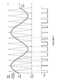
- FIG. 5 illustrates schematic graphs showing waveform timing relationships for the circuits shown in FIGS. 3 and 4 , according to specific example embodiments of this disclosure
- FIG. 6 illustrates a schematic block diagram of an integrated circuit microcontroller comprising a Class D power driver peripheral utilizing a DAC as a signal source, according to specific example embodiments of this disclosure
- FIG. 7 illustrates a schematic block diagram of a capacitive sensing module, according to specific example embodiments of this disclosure.
- FIG. 8 illustrates a schematic block diagram of another capacitive sensing module, according to specific example embodiments of this disclosure.
- an integrated Class D peripheral may be incorporated with a microcontroller for use in many different applications.
- Use of a simple triangle waveform (saw tooth) oscillator normally used for detecting changes in capacitance values in combination with a voltage comparator provides inexpensive generation of pulse width modulation (PWM) suitable for a wide range of Class D power applications.
- PWM pulse width modulation
- the open loop Class D power driver peripheral may comprise a digital-to-analog converter (DAC) 102 , a voltage comparator 104 , a complementary output generator (COG) 110 , a capacitive sensing module (CSM) 106 , a timing capacitor 126 , inverters 112 and 114 , and power metal oxide semiconductor field effect transistors (MOSFETs) 116 - 122 driving a load 124 .
- DAC digital-to-analog converter
- COG complementary output generator
- CSM capacitive sensing module
- MOSFETs power metal oxide semiconductor field effect transistors
- the DAC 102 may have its digital inputs coupled to a microcontroller (not shown) and provide analog control of the pulse width modulation (PWM) duty cycle to the COG 110 .
- the COG 110 is a peripheral having a single ended input and two complementary outputs (or four to eliminate the inverters 112 and 114 ).
- the purpose of the COG 110 is to provide two (or four) outputs and provide dead bands between assertions of the outputs so that there is no “current shoot through” of transistor pairs 116 , 118 and 120 , 122 , e.g., only one of the pairs may be on at a time by using “dead band control of the PWM waveforms to the power MOSFETs 116 - 122 .
- the CSM 106 and timing capacitor 126 may be used to generate a triangle waveform that is coupled to an input of the comparator 104 .
- a pulse width modulation (PWM) waveform may be generated.
- the duty cycle of the PWM waveform is dependent upon the analog voltage value from the DAC 102
- the frequency of the PWM waveform is dependent upon the frequency of the triangle wave from the CSM 106 .
- the CSM 106 is designed to generate an oscillation at a frequency determined by the capacitance value of the capacitor 126 . Normally the CSM 106 is used with capacitive touch key applications wherein the CSM frequency changes when the capacitance of the touch key changes.
- the change in frequency is measured and used as an indication of the capacitive key being touched.
- the triangle waveform oscillation from the CSM 106 is used as a triangle waveform reference input to the comparator 104 .
- the CSM 106 is a relaxation oscillator having a substantially triangular waveform.
- the capacitive sensing module (CSM) 106 may comprise a free-running RC relaxation oscillator using two comparators 752 and 754 , an SR latch 756 , resistor 758 , and capacitor 126 .
- the SR latch 756 is used to change the voltage charge direction, up or down, of the capacitor 126 . It will charge and discharge the capacitor 126 at a rate determined by an RC time constant defined by the feedback resistor 758 and capacitor 126 . This up and down charging will be between upper and lower limits set by the positive inputs to the comparators 752 and 754 .
- the time required to charge from the lower limit to the upper limit and discharge back to the lower limit is the period of the oscillator.
- the positive inputs of the comparators 752 and 754 are the upper and lower charging limits.
- the reference voltage, e.g., 2 ⁇ 3 Vdd, to the comparator 752 may be supplied internally, and the reference voltage to the comparator 754 may be supplied either externally (e.g., voltage divider resistors 760 and 762 ) to set the lower limit or from an internal voltage reference.
- the capacitor 764 may be used to reject high-frequency noise from the power supply and ensure a stable lower limit.
- the voltage at the capacitor 126 will charge and discharge between these limits, and may be driven by logic level signals from the /Q output of latch 756 .
- the output from comparator 754 may be configured to get the appropriate charging and discharging behavior.
- Feedback resistor 758 forms an RC time constant with the capacitor 126 .
- FIG. 8 depicted is a schematic block diagram of another capacitive sensing module, according to specific example embodiments of this disclosure.
- Another capacitive sensing module (CSM) 106 a may comprise a single comparator 850 with hysteresis, and first and second current sources 852 and 854 configured to run as a free running oscillator with the timing capacitor 126 determining the frequency thereof.
- the single comparator 850 with hysteresis has two voltage limits, a high and a low voltage limit that its input may change between before the output of the comparator 850 changes state. When the output of the comparator 850 is high the charging current source may be enabled, and when the output of the comparator 850 is low the discharging current source may be enabled.
- CSM 106 or CSM 106 a may be used interchangeably as discussed throughout this disclosure and as shown in FIGS. 1-4 and 6 . It is contemplated and within the scope of this disclosure that other circuit designs may be used for the CSM 106 or 106 a , and one having ordinary skill in electronic circuit design and the benefit of this disclosure could design such circuits.
- the power MOSFETs 116 - 122 may be configured as a full-bridge H and drive the load 124 , e.g., motor, transducer, solenoid and piezo electric actuators, speaker, and the like.
- a half-bridge may also be used and is contemplated herein.
- the amount of power supplied to the load 124 through the power MOSFETs 116 - 122 may be controlled by the analog output voltage of the DAC 102 and may be varied according to the application requirements.
- low pass filters (not shown) may be coupled between the terminals of the load 124 and the junctions of the MOSFET pairs 116 , 118 and 120 , 122 .
- the DAC 102 , comparator 104 , CSM 106 , COG 110 , and inverters 112 and 114 may be provided in a mixed signal (analog and digital) microcontroller, as manufactured by Applicant.
- output drivers (not shown), instead of the MOSFETs 116 - 122 , may also be provided with the microcontroller.
- the timing capacitor 126 may be external and selected for a desired (triangle waveform) PWM frequency.
- the closed loop Class D power driver peripheral may comprise a digital-to-analog converter (DAC) 102 , a voltage comparator 104 , a complementary output generator (COG) 110 , a capacitive sensing module (CSM) 106 , a timing capacitor 126 , inverters 112 and 114 , and power metal oxide semiconductor field effect transistors (MOSFETs) 116 - 122 driving a load 124 .
- DAC digital-to-analog converter
- COG complementary output generator
- CSM capacitive sensing module
- MOSFETs power metal oxide semiconductor field effect transistors
- the closed loop Class D power driver peripheral 200 functions substantially the same as described above for the circuit shown in FIG. 1 with the addition of a close loop feedback circuit comprising a differential amplifier 230 having inputs coupled to the terminals of the load 124 and driving an operational amplifier 232 having closed loop compensation components resistor 240 , and capacitors 236 and 238 .
- the closed loop compensation components form a compensation network, e.g., they provide feedback to guarantee that the actual drive to the load 124 matches the input signal.
- the output network (load 124 ) is an LC (inductor and optional capacitor), and the feedback is negative, there is the possibility of instability and oscillation caused by the feedback, so the purpose of the combination of resistor 240 and capacitors 236 and 238 in the compensation network is to provide sufficient gain and phase shift to insure stability and fidelity to the original input signal.
- the gain of the operational amplifier may be determined by resistor 234 in combination with the compensation network (resistor 240 and capacitors 236 and 238 ). The output to the load 124 may thereby be closed loop compensated and subtracted from the DAC 102 output with the operational amplifier 232 .
- FIG. 3 depicted is a schematic block diagram of a circuit for an open loop Class D audio power driver peripheral utilizing an external signal source, according yet another specific example embodiment of this disclosure.
- the DAC 102 has been replaced by an analog input signal, e.g., audio signal, which may be a time varying analog voltage applied to an input of the comparator 104 .
- a PWM waveform representative of the analog input signal is thereby generated and coupled to the COG 110 for driving the power MOSFETs 116 - 122 .
- FIG. 4 depicted is a schematic block diagram of a circuit for a closed loop Class D audio power driver peripheral utilizing an external signal source, according still another specific example embodiment of this disclosure.
- the DAC 102 has been replaced by an analog input signal, e.g., audio signal, which may be a time varying analog voltage applied to an input of the comparator 104 .
- a PWM waveform representative of the analog input signal is thereby generated and coupled to the COG 110 for driving the power MOSFETs 116 - 122 .
- the Class D audio power driver peripherals shown in FIGS. 3 and 4 operate in substantially the same way as the Class D power driver peripherals shown in FIGS. 1 and 2 , respectively, except that the analog voltage applied to an input of the comparator 104 is time varying and not a constant DC set point from the DAC 102 .
- FIG. 5 depicted are schematic graphs showing waveform timing relationships of the circuits shown in FIGS. 3 and 4 , according to specific example embodiments of this disclosure.
- the audio input and triangular wave are both centered around 0 volts, so that for an analog audio input at zero (0) volts, the duty ratio of the PWM output pulses is approximately 50 percent.
- the audio amplitude exceeds that of the triangle wave, full modulation occurs (100 percent on or off pulse width), where the pulse train stops switching, and the duty ratio within individual periods is either zero (0) percent or 100 percent.
- FIG. 6 depicted is a schematic block diagram of an integrated circuit microcontroller comprising a Class D power driver peripheral utilizing a DAC as a signal source, according to specific example embodiments of this disclosure.
- An integrated circuit (IC) microcontroller 640 comprising a digital processor 642 and memory 644 , and the Class D power driver peripherals shown in FIGS. 1-4 may be used as a cost effective solution for many Class D power applications.
- An internal configuration switch 646 (solid state) may also be included in the microcontroller 640 for increased versatility by allowing the microcontroller 640 to be used for either Class D audio or Class D control applications, e.g., motors and actuators.
- the COG 610 may have four outputs that eliminate the requirement for the two inverters 112 and 114 , but otherwise operates substantially the same as the COG 110 described more fully hereinabove.
- the power MOSFETs 116 - 122 may be replaced by output drivers (not shown) that may be included in the microcontroller 640 die/package.
Landscapes
- Engineering & Computer Science (AREA)
- Power Engineering (AREA)
- Multimedia (AREA)
- Amplifiers (AREA)
Abstract
Description
Claims (21)
Priority Applications (6)
| Application Number | Priority Date | Filing Date | Title |
|---|---|---|---|
| US14/536,916 US9543899B2 (en) | 2014-11-10 | 2014-11-10 | Class D power driver peripheral |
| PCT/US2015/059657 WO2016077188A1 (en) | 2014-11-10 | 2015-11-09 | Class d power driver peripheral |
| EP15797544.2A EP3219008A1 (en) | 2014-11-10 | 2015-11-09 | Class d power driver peripheral |
| KR1020177008343A KR20170084017A (en) | 2014-11-10 | 2015-11-09 | Class d power driver peripheral |
| CN201580057640.9A CN107078697A (en) | 2014-11-10 | 2015-11-09 | D class analog line driver ancillary equipment |
| TW104137075A TW201620247A (en) | 2014-11-10 | 2015-11-10 | Class D power driver peripheral |
Applications Claiming Priority (1)
| Application Number | Priority Date | Filing Date | Title |
|---|---|---|---|
| US14/536,916 US9543899B2 (en) | 2014-11-10 | 2014-11-10 | Class D power driver peripheral |
Publications (2)
| Publication Number | Publication Date |
|---|---|
| US20160134239A1 US20160134239A1 (en) | 2016-05-12 |
| US9543899B2 true US9543899B2 (en) | 2017-01-10 |
Family
ID=54602048
Family Applications (1)
| Application Number | Title | Priority Date | Filing Date |
|---|---|---|---|
| US14/536,916 Expired - Fee Related US9543899B2 (en) | 2014-11-10 | 2014-11-10 | Class D power driver peripheral |
Country Status (6)
| Country | Link |
|---|---|
| US (1) | US9543899B2 (en) |
| EP (1) | EP3219008A1 (en) |
| KR (1) | KR20170084017A (en) |
| CN (1) | CN107078697A (en) |
| TW (1) | TW201620247A (en) |
| WO (1) | WO2016077188A1 (en) |
Families Citing this family (5)
| Publication number | Priority date | Publication date | Assignee | Title |
|---|---|---|---|---|
| US10312872B2 (en) | 2017-04-28 | 2019-06-04 | Aura Semiconductor Pvt. Ltd | Managing a shoot-through condition in a component containing a push-pull output stage |
| JP7055659B2 (en) * | 2018-02-15 | 2022-04-18 | 東芝テック株式会社 | Liquid circulation device and liquid discharge device |
| CN108718198B (en) * | 2018-08-07 | 2023-11-03 | 上海艾为电子技术股份有限公司 | Digital-analog converter |
| US11571803B2 (en) * | 2019-05-30 | 2023-02-07 | Milwaukee Electric Tool Corporation | Power tool with combined chip for wireless communications and power tool control |
| US11271480B2 (en) * | 2020-08-03 | 2022-03-08 | xMEMS Labs, Inc. | Driving circuit with energy recycle capability and method thereof |
Citations (9)
| Publication number | Priority date | Publication date | Assignee | Title |
|---|---|---|---|---|
| US5973368A (en) | 1996-06-05 | 1999-10-26 | Pearce; Lawrence G. | Monolithic class D amplifier |
| US20080315948A1 (en) | 2007-06-20 | 2008-12-25 | Nokia Corporation | Circuit architecture having differential processing for use in half bridges and full bridges and methods therefore |
| US20120056552A1 (en) * | 2010-09-03 | 2012-03-08 | Bo Yu | Multi-mode dimming circuit |
| US20120294473A1 (en) * | 2011-05-09 | 2012-11-22 | Pierce Harold D | Low cost programmable sound recording and playback device and method for communicating with, and recharging of, the device |
| US20130154670A1 (en) * | 2011-12-14 | 2013-06-20 | Microchip Technology Incorporated | Method and Apparatus for Detecting Smoke in an ION Chamber |
| US20130216076A1 (en) * | 2011-02-28 | 2013-08-22 | Widex A/S | Hearing aid and method of driving an output stage |
| US20130335143A1 (en) * | 2012-06-14 | 2013-12-19 | Princeton Technology Corporation | Class-d power amplifier capable of reducing electromagnetic interference and triangular wave generator thereof |
| US20150155839A1 (en) * | 2013-12-02 | 2015-06-04 | Crestron Electronics, Inc. | Reducing Crosstalk and Matched Output Power Audio Amplfiers |
| US20150180430A1 (en) * | 2013-12-20 | 2015-06-25 | Broadcom Corporation | Digital class-d amplifier with analog feedback |
Family Cites Families (2)
| Publication number | Priority date | Publication date | Assignee | Title |
|---|---|---|---|---|
| EP0830728A2 (en) * | 1995-06-07 | 1998-03-25 | Harris Corporation | Monolithic class d amplifier |
| CN100471044C (en) * | 2007-03-08 | 2009-03-18 | 埃派克森微电子(上海)有限公司 | Frequency switching circuit and method for suppressing class D power amplifier POP sound |
-
2014
- 2014-11-10 US US14/536,916 patent/US9543899B2/en not_active Expired - Fee Related
-
2015
- 2015-11-09 WO PCT/US2015/059657 patent/WO2016077188A1/en not_active Ceased
- 2015-11-09 EP EP15797544.2A patent/EP3219008A1/en not_active Withdrawn
- 2015-11-09 KR KR1020177008343A patent/KR20170084017A/en not_active Withdrawn
- 2015-11-09 CN CN201580057640.9A patent/CN107078697A/en active Pending
- 2015-11-10 TW TW104137075A patent/TW201620247A/en unknown
Patent Citations (9)
| Publication number | Priority date | Publication date | Assignee | Title |
|---|---|---|---|---|
| US5973368A (en) | 1996-06-05 | 1999-10-26 | Pearce; Lawrence G. | Monolithic class D amplifier |
| US20080315948A1 (en) | 2007-06-20 | 2008-12-25 | Nokia Corporation | Circuit architecture having differential processing for use in half bridges and full bridges and methods therefore |
| US20120056552A1 (en) * | 2010-09-03 | 2012-03-08 | Bo Yu | Multi-mode dimming circuit |
| US20130216076A1 (en) * | 2011-02-28 | 2013-08-22 | Widex A/S | Hearing aid and method of driving an output stage |
| US20120294473A1 (en) * | 2011-05-09 | 2012-11-22 | Pierce Harold D | Low cost programmable sound recording and playback device and method for communicating with, and recharging of, the device |
| US20130154670A1 (en) * | 2011-12-14 | 2013-06-20 | Microchip Technology Incorporated | Method and Apparatus for Detecting Smoke in an ION Chamber |
| US20130335143A1 (en) * | 2012-06-14 | 2013-12-19 | Princeton Technology Corporation | Class-d power amplifier capable of reducing electromagnetic interference and triangular wave generator thereof |
| US20150155839A1 (en) * | 2013-12-02 | 2015-06-04 | Crestron Electronics, Inc. | Reducing Crosstalk and Matched Output Power Audio Amplfiers |
| US20150180430A1 (en) * | 2013-12-20 | 2015-06-25 | Broadcom Corporation | Digital class-d amplifier with analog feedback |
Non-Patent Citations (5)
| Title |
|---|
| Aleman, Enrique, "AN1171: Using the Capacitive Sensing Module on the PIC16F72X," Microchip Technology Incorporated, 8 pages, Jan. 2, 2008. |
| Davison, Burke, "AN1334: Techniques for Robust Touch Sensing Design," Microchip Technology Incorporated, 30 pages, Nov. 29, 2012. |
| International Search Report and Written Opinion, Application No. PCT/US2015/059657, 11 pages, Feb. 11, 2016. |
| Perme, Thomas, "AN1101: Introduction to Capacitive Sensing," Microchip Technology Incorporated, 10 pages, © 2007. |
| Perme, Thomas, "AN1268: mTouchTM Capacitive Sensing Using Period Method," Microchip Technology Incorporated, 8 pages, © 2009. |
Also Published As
| Publication number | Publication date |
|---|---|
| EP3219008A1 (en) | 2017-09-20 |
| WO2016077188A1 (en) | 2016-05-19 |
| TW201620247A (en) | 2016-06-01 |
| CN107078697A (en) | 2017-08-18 |
| US20160134239A1 (en) | 2016-05-12 |
| KR20170084017A (en) | 2017-07-19 |
Similar Documents
| Publication | Publication Date | Title |
|---|---|---|
| US8405465B2 (en) | Duty cycle translator methods and apparatus | |
| US9543899B2 (en) | Class D power driver peripheral | |
| US9564862B2 (en) | Class D audio amplifier with adjustable loop filter characteristics | |
| US6847257B2 (en) | Efficient minimum pulse spread spectrum modulation for filterless class D amplifiers | |
| CN107070423B (en) | Method and apparatus for achieving high output signal swing for class D amplifiers | |
| CN102984630B (en) | For reducing the system and method for distortion in audio amplifier system | |
| US20110121765A1 (en) | Driver for piezoelectric actuator | |
| US7741914B1 (en) | Amplifier system with dynamically-adjusted supply voltage | |
| US11277129B2 (en) | Driver circuitry and operation | |
| US20230412976A1 (en) | Driver circuits | |
| US11684950B2 (en) | Driver circuitry and operation | |
| US20130099859A1 (en) | Multilevel Class-D Amplifier | |
| US11835037B2 (en) | Methods and devices for driving a piezoelectric pump | |
| JP2016119700A (en) | Semiconductor device | |
| US7323919B2 (en) | Pulse-width modulation circuits of self-oscillation type and pulse-width modulation methods | |
| US9263992B1 (en) | Class D amplifier with variable switching frequency | |
| US6828836B1 (en) | Two comparator voltage mode PWM | |
| CN106249792B (en) | The operating method of voltage regulator circuit and voltage regulator circuit | |
| KR101404568B1 (en) | Current mode controlled pulse width modulation converter | |
| US9806682B1 (en) | Multilevel class-D amplifiers | |
| US7046727B2 (en) | Method and apparatus for self-oscillating differential feedback class-D amplifier | |
| US7986179B2 (en) | Circuit and method for reducing popping sound | |
| US9667208B2 (en) | Class-D amplifier and electronic apparatus | |
| JP2022191867A (en) | Control circuit of dc/dc converter, power supply circuit, and electronic apparatus | |
| JP2014220059A (en) | High-frequency power supply |
Legal Events
| Date | Code | Title | Description |
|---|---|---|---|
| AS | Assignment |
Owner name: MICROCHIP TECHNOLOGY INCORPORATED, ARIZONA Free format text: ASSIGNMENT OF ASSIGNORS INTEREST;ASSIGNOR:CURTIS, KEITH E.;REEL/FRAME:034478/0460 Effective date: 20141106 |
|
| STCF | Information on status: patent grant |
Free format text: PATENTED CASE |
|
| AS | Assignment |
Owner name: JPMORGAN CHASE BANK, N.A., AS ADMINISTRATIVE AGENT, ILLINOIS Free format text: SECURITY INTEREST;ASSIGNOR:MICROCHIP TECHNOLOGY INCORPORATED;REEL/FRAME:041675/0617 Effective date: 20170208 Owner name: JPMORGAN CHASE BANK, N.A., AS ADMINISTRATIVE AGENT Free format text: SECURITY INTEREST;ASSIGNOR:MICROCHIP TECHNOLOGY INCORPORATED;REEL/FRAME:041675/0617 Effective date: 20170208 |
|
| AS | Assignment |
Owner name: JPMORGAN CHASE BANK, N.A., AS ADMINISTRATIVE AGENT, ILLINOIS Free format text: SECURITY INTEREST;ASSIGNORS:MICROCHIP TECHNOLOGY INCORPORATED;SILICON STORAGE TECHNOLOGY, INC.;ATMEL CORPORATION;AND OTHERS;REEL/FRAME:046426/0001 Effective date: 20180529 Owner name: JPMORGAN CHASE BANK, N.A., AS ADMINISTRATIVE AGENT Free format text: SECURITY INTEREST;ASSIGNORS:MICROCHIP TECHNOLOGY INCORPORATED;SILICON STORAGE TECHNOLOGY, INC.;ATMEL CORPORATION;AND OTHERS;REEL/FRAME:046426/0001 Effective date: 20180529 |
|
| AS | Assignment |
Owner name: WELLS FARGO BANK, NATIONAL ASSOCIATION, AS NOTES COLLATERAL AGENT, CALIFORNIA Free format text: SECURITY INTEREST;ASSIGNORS:MICROCHIP TECHNOLOGY INCORPORATED;SILICON STORAGE TECHNOLOGY, INC.;ATMEL CORPORATION;AND OTHERS;REEL/FRAME:047103/0206 Effective date: 20180914 Owner name: WELLS FARGO BANK, NATIONAL ASSOCIATION, AS NOTES C Free format text: SECURITY INTEREST;ASSIGNORS:MICROCHIP TECHNOLOGY INCORPORATED;SILICON STORAGE TECHNOLOGY, INC.;ATMEL CORPORATION;AND OTHERS;REEL/FRAME:047103/0206 Effective date: 20180914 |
|
| FEPP | Fee payment procedure |
Free format text: MAINTENANCE FEE REMINDER MAILED (ORIGINAL EVENT CODE: REM.); ENTITY STATUS OF PATENT OWNER: LARGE ENTITY |
|
| LAPS | Lapse for failure to pay maintenance fees |
Free format text: PATENT EXPIRED FOR FAILURE TO PAY MAINTENANCE FEES (ORIGINAL EVENT CODE: EXP.); ENTITY STATUS OF PATENT OWNER: LARGE ENTITY |
|
| STCH | Information on status: patent discontinuation |
Free format text: PATENT EXPIRED DUE TO NONPAYMENT OF MAINTENANCE FEES UNDER 37 CFR 1.362 |
|
| FP | Lapsed due to failure to pay maintenance fee |
Effective date: 20210110 |
|
| AS | Assignment |
Owner name: MICROSEMI STORAGE SOLUTIONS, INC., ARIZONA Free format text: RELEASE BY SECURED PARTY;ASSIGNOR:JPMORGAN CHASE BANK, N.A., AS ADMINISTRATIVE AGENT;REEL/FRAME:059333/0222 Effective date: 20220218 Owner name: MICROSEMI CORPORATION, ARIZONA Free format text: RELEASE BY SECURED PARTY;ASSIGNOR:JPMORGAN CHASE BANK, N.A., AS ADMINISTRATIVE AGENT;REEL/FRAME:059333/0222 Effective date: 20220218 Owner name: ATMEL CORPORATION, ARIZONA Free format text: RELEASE BY SECURED PARTY;ASSIGNOR:JPMORGAN CHASE BANK, N.A., AS ADMINISTRATIVE AGENT;REEL/FRAME:059333/0222 Effective date: 20220218 Owner name: SILICON STORAGE TECHNOLOGY, INC., ARIZONA Free format text: RELEASE BY SECURED PARTY;ASSIGNOR:JPMORGAN CHASE BANK, N.A., AS ADMINISTRATIVE AGENT;REEL/FRAME:059333/0222 Effective date: 20220218 Owner name: MICROCHIP TECHNOLOGY INCORPORATED, ARIZONA Free format text: RELEASE BY SECURED PARTY;ASSIGNOR:JPMORGAN CHASE BANK, N.A., AS ADMINISTRATIVE AGENT;REEL/FRAME:059333/0222 Effective date: 20220218 Owner name: MICROCHIP TECHNOLOGY INCORPORATED, ARIZONA Free format text: RELEASE OF SECURITY INTEREST;ASSIGNOR:JPMORGAN CHASE BANK, N.A., AS ADMINISTRATIVE AGENT;REEL/FRAME:059333/0222 Effective date: 20220218 Owner name: SILICON STORAGE TECHNOLOGY, INC., ARIZONA Free format text: RELEASE OF SECURITY INTEREST;ASSIGNOR:JPMORGAN CHASE BANK, N.A., AS ADMINISTRATIVE AGENT;REEL/FRAME:059333/0222 Effective date: 20220218 Owner name: ATMEL CORPORATION, ARIZONA Free format text: RELEASE OF SECURITY INTEREST;ASSIGNOR:JPMORGAN CHASE BANK, N.A., AS ADMINISTRATIVE AGENT;REEL/FRAME:059333/0222 Effective date: 20220218 Owner name: MICROSEMI CORPORATION, ARIZONA Free format text: RELEASE OF SECURITY INTEREST;ASSIGNOR:JPMORGAN CHASE BANK, N.A., AS ADMINISTRATIVE AGENT;REEL/FRAME:059333/0222 Effective date: 20220218 Owner name: MICROSEMI STORAGE SOLUTIONS, INC., ARIZONA Free format text: RELEASE OF SECURITY INTEREST;ASSIGNOR:JPMORGAN CHASE BANK, N.A., AS ADMINISTRATIVE AGENT;REEL/FRAME:059333/0222 Effective date: 20220218 |
|
| AS | Assignment |
Owner name: MICROCHIP TECHNOLOGY INCORPORATED, ARIZONA Free format text: RELEASE BY SECURED PARTY;ASSIGNOR:JPMORGAN CHASE BANK, N.A., AS ADMINISTRATIVE AGENT;REEL/FRAME:059666/0545 Effective date: 20220218 |
|
| AS | Assignment |
Owner name: MICROSEMI STORAGE SOLUTIONS, INC., ARIZONA Free format text: RELEASE BY SECURED PARTY;ASSIGNOR:WELLS FARGO BANK, NATIONAL ASSOCIATION, AS NOTES COLLATERAL AGENT;REEL/FRAME:059358/0001 Effective date: 20220228 Owner name: MICROSEMI CORPORATION, ARIZONA Free format text: RELEASE BY SECURED PARTY;ASSIGNOR:WELLS FARGO BANK, NATIONAL ASSOCIATION, AS NOTES COLLATERAL AGENT;REEL/FRAME:059358/0001 Effective date: 20220228 Owner name: ATMEL CORPORATION, ARIZONA Free format text: RELEASE BY SECURED PARTY;ASSIGNOR:WELLS FARGO BANK, NATIONAL ASSOCIATION, AS NOTES COLLATERAL AGENT;REEL/FRAME:059358/0001 Effective date: 20220228 Owner name: SILICON STORAGE TECHNOLOGY, INC., ARIZONA Free format text: RELEASE BY SECURED PARTY;ASSIGNOR:WELLS FARGO BANK, NATIONAL ASSOCIATION, AS NOTES COLLATERAL AGENT;REEL/FRAME:059358/0001 Effective date: 20220228 Owner name: MICROCHIP TECHNOLOGY INCORPORATED, ARIZONA Free format text: RELEASE BY SECURED PARTY;ASSIGNOR:WELLS FARGO BANK, NATIONAL ASSOCIATION, AS NOTES COLLATERAL AGENT;REEL/FRAME:059358/0001 Effective date: 20220228 Owner name: MICROCHIP TECHNOLOGY INCORPORATED, ARIZONA Free format text: RELEASE OF SECURITY INTEREST;ASSIGNOR:WELLS FARGO BANK, NATIONAL ASSOCIATION, AS NOTES COLLATERAL AGENT;REEL/FRAME:059358/0001 Effective date: 20220228 Owner name: SILICON STORAGE TECHNOLOGY, INC., ARIZONA Free format text: RELEASE OF SECURITY INTEREST;ASSIGNOR:WELLS FARGO BANK, NATIONAL ASSOCIATION, AS NOTES COLLATERAL AGENT;REEL/FRAME:059358/0001 Effective date: 20220228 Owner name: ATMEL CORPORATION, ARIZONA Free format text: RELEASE OF SECURITY INTEREST;ASSIGNOR:WELLS FARGO BANK, NATIONAL ASSOCIATION, AS NOTES COLLATERAL AGENT;REEL/FRAME:059358/0001 Effective date: 20220228 Owner name: MICROSEMI CORPORATION, ARIZONA Free format text: RELEASE OF SECURITY INTEREST;ASSIGNOR:WELLS FARGO BANK, NATIONAL ASSOCIATION, AS NOTES COLLATERAL AGENT;REEL/FRAME:059358/0001 Effective date: 20220228 Owner name: MICROSEMI STORAGE SOLUTIONS, INC., ARIZONA Free format text: RELEASE OF SECURITY INTEREST;ASSIGNOR:WELLS FARGO BANK, NATIONAL ASSOCIATION, AS NOTES COLLATERAL AGENT;REEL/FRAME:059358/0001 Effective date: 20220228 |