US9535140B2 - System and method for a transformer and a phase-shift network - Google Patents
System and method for a transformer and a phase-shift network Download PDFInfo
- Publication number
- US9535140B2 US9535140B2 US13/931,092 US201313931092A US9535140B2 US 9535140 B2 US9535140 B2 US 9535140B2 US 201313931092 A US201313931092 A US 201313931092A US 9535140 B2 US9535140 B2 US 9535140B2
- Authority
- US
- United States
- Prior art keywords
- node
- coupled
- circuit
- signal
- impedance
- Prior art date
- Legal status (The legal status is an assumption and is not a legal conclusion. Google has not performed a legal analysis and makes no representation as to the accuracy of the status listed.)
- Active, expires
Links
Images


Classifications
-
- G—PHYSICS
- G01—MEASURING; TESTING
- G01R—MEASURING ELECTRIC VARIABLES; MEASURING MAGNETIC VARIABLES
- G01R33/00—Arrangements or instruments for measuring magnetic variables
- G01R33/02—Measuring direction or magnitude of magnetic fields or magnetic flux
- G01R33/06—Measuring direction or magnitude of magnetic fields or magnetic flux using galvano-magnetic devices
- G01R33/09—Magnetoresistive devices
-
- H—ELECTRICITY
- H03—ELECTRONIC CIRCUITRY
- H03H—IMPEDANCE NETWORKS, e.g. RESONANT CIRCUITS; RESONATORS
- H03H7/00—Multiple-port networks comprising only passive electrical elements as network components
- H03H7/18—Networks for phase shifting
-
- H—ELECTRICITY
- H03—ELECTRONIC CIRCUITRY
- H03H—IMPEDANCE NETWORKS, e.g. RESONANT CIRCUITS; RESONATORS
- H03H7/00—Multiple-port networks comprising only passive electrical elements as network components
- H03H7/38—Impedance-matching networks
- H03H7/40—Automatic matching of load impedance to source impedance
Definitions
- the present disclosure relates generally to an electronic device, and more particularly to a system and method for a transformer and a phase-shift network.
- Directional couplers which are electronic devices that can detect power being transmitted in a particular direction, are used in a wide variety of radio frequency (RF) circuits.
- RF radio frequency
- a directional coupler may be used in a radar system to detect a reflected wave by separating the indecent wave from the reflected wave, or may be used in a circuit that measures the impedance mismatch of transmission lines.
- a directional coupler has a forward transmission path and a coupled transmission path.
- the forward transmission path generally has a low loss, while the coupled transmission path couples a fraction of the transmission power that is propagated in a particular direction.
- coupler architectures that include electromagnetic couples and magnetic couplers. Each of these coupler types may be implemented using different topologies and materials depending on the frequency of operation and the operational environment.
- a directional coupler may be implemented using stripline structures disposed on a printed circuit board (PCB) or transformers.
- PCB printed circuit board
- various circuit elements may be as long as a quarter wavelength of the particular signal being measured.
- constructing stripline directional couplers on an integrated circuit becomes challenging dues to the wavelengths at these frequencies being much longer than the feature sizes on the integrated circuit.
- Low-loss magnetic-based directional couplers also are challenging to construct at this range of frequencies because of transformer losses and parasitics.
- a circuit in accordance with an embodiment, includes a magnetic transformer having a first winding coupled between a first signal node and a second signal node, and a second winding coupled between a first reference node and a current measurement node.
- a phase shift network is coupled between the second node and a voltage measurement node, and the circuit is configured to indicate an impedance matching condition based on an amplitude difference and a phase difference between the voltage measurement node and the current measurement node.
- FIGS. 1 a - c illustrates an embodiment coupler circuits
- FIGS. 2 a - b illustrate waveform diagrams corresponding to an embodiment coupler circuit
- FIGS. 3 a - b illustrate embodiment incident and reflected wave measurement circuits
- FIGS. 4 a - d illustrate further embodiment incident and reflected wave measurement circuits
- FIG. 5 illustrates an implementation of an embodiment coupler on metallization layers
- FIGS. 6 a - c illustrate various embodiment RF systems
- FIGS. 7 a - b illustrate block diagrams of embodiment methods
- FIGS. 8 a - b illustrate further embodiment incident and reflected wave measurement circuits.
- the present invention will be described with respect to preferred embodiments in a specific context, a system and method for a directional coupler that may be used in RF circuits to measure incident or reflected power.
- the invention may also be applied to other systems and applications including other circuits that make RF measurements including, but not limited to devices that measure and/or tune impedance mismatch, time domain reflectometers (TDR), sensing devices for use with tunable antenna matching circuits, and tunable filters.
- TDR time domain reflectometers
- an impedance measurement device includes a phase-shift network coupled to transformer having a primary winding and secondary winding.
- the primary winding of the transformer is coupled in series with a transmission path of the impedance measurement device.
- the secondary winding of the transformer and the phase shifter is loaded by high-impedance measurement device that determines the quality of the impedance match and/or the absolute or relative magnitude and/or phase of an incident and/or reflected signal between ports of the transmission path.
- information about the amplitude and phase of current and voltage of the RF signal is extracted and compared with a predefined value, such as, but not limited to a 50 ⁇ impedance.
- a predefined value such as, but not limited to a 50 ⁇ impedance.
- the relationship between the extracted amplitudes and phases of the RF current and voltage indicates the amount of reflection in the RF signal path and therefore indicates the load impedance. For example, the smaller the reflection, the closer the load impedance is close to the characteristic impedance Z 0 :
- a magnetic transformer generates a voltage proportional to an RF current and an RC network generates voltage proportional to an RF voltage.
- the coupler is constructed such that amplitudes and phases of the voltage proportional to the RF current and the voltage proportional to the RF voltage are 180 degrees out of phase and have the same amplitude when there is no reflection in the RF signal path.
- the coupler 1 is a four-port device with ports 2 and 3 being the 50-Ohm ports for RF signal and two coupled ports 4 and 5 loaded with a high impedance.
- Coupler 1 includes transformer X 1 with primary winding Lp coupled between source impedance Z S and load impedance Z L .
- a phase-shifting network implemented by a high-pass RC filter that includes resistor R 1 and capacitor C 1 is coupled to the port 3 .
- V i ⁇ j ⁇ k ⁇ square root over ( L P L s ) ⁇ I RF , (1)
- L p and L s are the self-inductance of primary and secondary windings of transformer X 1
- k is a coupling factor between primary and secondary windings of X 1 .
- the voltage Vv at port 4 can be expressed as:
- V v j ⁇ ⁇ ⁇ R 1 ⁇ C 1 j ⁇ ⁇ ⁇ R 1 ⁇ C 1 + 1 ⁇ V RF ( 2 )
- equation (2) may be approximated as follows: V v ⁇ j ⁇ R 1 C 1 ⁇ V RF . (4)
- the various components and parameters k, L P , L S , R 1 and C 1 are chosen to meet the following condition:
- Z 0 is a reference impedance.
- and ⁇ V v ⁇ V i 180°. In the case of an impedance mismatch, for example, when Z L ⁇ Z 0 , V v +V i ⁇ 0. (6b)
- FIG. 1 b illustrates a further embodiment in which the phase-shifting network is coupled to source impedance Z S via port 2 and transformer X 1 is coupled to load impedance Z L via port 3
- FIG. 1 c illustrates an alternative embodiment in which the phase shifting network is tapped to the first winding of transformer X 1 .
- FIGS. 2 a - b include waveform diagrams that illustrate the relationship between voltages Vi and Vv under matched impedance conditions and mismatched impedance conditions with respect to the circuit of FIG. 1 a .
- FIG. 2 a illustrates a waveform diagram showing the relationship between the input and output currents measurement output voltages of an embodiment coupler under matched impedance conditions. As shown, current I RF and voltage V RF are in-phase with each other with relative amplitudes that follow the following relationship:
- V RF I RF Z 0 . Consequently, voltages Vi and Vv at port 5 and port 4 respectively have equal amplitudes and are 180 degrees out of phase with each other such that the sum of Vi and Vv is zero and/or is a DC voltage.
- the node at port 5 that produces Vi may be referred to as a current measurement node
- the node at port 4 that produces Vv may be referred to as a voltage measurement node.
- FIG. 2 b illustrates a waveform diagram showing the relationship between the input and output currents measurement output voltages of an embodiment coupler under mismatched impedance conditions. As shown, current I RF and voltage V RF are out of phase with each other with relative amplitudes in which:
- V RF I RF ⁇ Z 0 voltages Vi and Vv at port 5 and port 4 , respectively have unequal amplitudes and are not 180 degrees out of phase with each other. Therefore, the sum of Vi and Vv has an AC component. It should be understood that the sum of Vi and Vv may have an AC components in conditions in which Vi and Vv are in phase with each other but have unequal amplitudes, or under conditions in which Vi and Vv are out of phase with each other but have equal amplitudes. In alternative embodiments, the amplitudes and phases of Vi and Vv may be scaled such an unequal amplitude condition and/or an out of phase condition represents a matched impedance conditions.
- phase shift networks that do not produce a 90° phase shift, amplitude scaling networks that produce non-equal amplitudes at matched conditions
- embodiments that omit analog phase shift networks.
- Such embodiments may occur due to the presence of device parasitics and/or may result in situations where component values and parameters are constrained to make a 90° phase shift and matched amplitude for Vi and Vv under matched impedance conditions impractical.
- the requisite scaling and phase shift needed to determine a matched impedance condition may be performed during post-processing in the analog or digital domain.
- Embodiment couplers and impedance mismatch measurement circuits may be used to monitor incident and reflected RF power.
- port 2 is considered an input port and port 3 is a transmission port then the sum of signals Vv and Vi will indicate the reflected power such that the difference between Vv and Vi is proportional to incident power.
- Vv and Vi is proportional to incident power.
- V RF V RF + + V RF - ( 7 )
- V RF + and I RF + are incident voltage and current
- V RF ⁇ and I RF ⁇ are the reflected voltage and current.
- V i - j ⁇ ⁇ k ⁇ L p ⁇ L s ⁇ V RF + Z 0 + j ⁇ ⁇ k ⁇ L p ⁇ L s ⁇ V RF - Z 0 , ⁇ and ( 9 ) V v ⁇ j ⁇ ⁇ ⁇ R 1 ⁇ C 1 ⁇ V RF + + j ⁇ ⁇ ⁇ R 1 ⁇ C 1 ⁇ V RF - . ( 10 ) According to (5):
- the sum of signals Vv and Vi indicates the incident power and difference between Vv and Vi indicates the reflected power.
- FIGS. 3 a - b illustrate an embodiment reflection measurement circuit having embodiment coupler 1 coupled to summing blocks 104 and 106 .
- Summing block 104 is configured to subtract Vi from Vv to produce an incident wave signal and summing block 106 is configured to add Vv to Vi to produce a reflected wave signal where the direction of the incident wave is from port 2 to port 3 .
- FIG. 3 b illustrates the case in which the incident wave propagates from port 3 to port 2 , in which case summing block 104 produces a signal proportional to the reflected wave and summing block 106 produces a signal proportional to the incident wave.
- FIGS. 4 a - d illustrate various embodiment mismatch detection systems utilizing embodiment coupler circuits.
- FIG. 4 a illustrates coupler 1 coupled to summing resistors R 2 and R 3 via ports 5 and 4 , respectively.
- RF power detector circuit 10 is coupled to resistors R 2 and R 3 at node V ref .
- RF power detector circuit 10 may be implemented using various power detection circuits known in the art.
- RF power detector 10 may be implemented using a simple diode power detector, a logarithmic power detector or other power detector circuits.
- power detector circuit 10 may produce an analog and/or digital value that is proportional to the amount of power detected by RF power detector 10 .
- the detected power may be, for example, proportional to the root mean square (RMS) voltage detected by power detector 10 .
- RMS root mean square
- voltage level detected by power detector 10 is zero, or substantially close to zero in conditions when source impedance Z S matches load impedance Z L and/or reference impedance Z 0 .
- power detector 10 may be omitted and node V ref be used as a directional coupler output for various applications.
- incident power monitoring using an embodiment coupler circuit may be performed by an active circuitry using voltages—Vi and Vv.
- the embodiment of FIG. 4 b includes coupler 1 , summing resistors R 2 and R 3 connected to ports 4 and 6 , respectively of coupler 1 , and RF power detector 11 .
- the embodiment of FIG. 4 b is similar to the embodiment of FIG. 4 a , with the exception that the output of secondary winding L S is taken from an opposite end of the winding. This produces a voltage—Vi that is 180 degrees out of phase with voltage Vi, and is in-phase with voltage Vv under matched impedance conditions.
- Voltages—Vi and Vv are summed on resistors R 2 and R 3 , which effectively subtracts Vi from Vv.
- a value proportional to the detected power of voltage V inc is derived based the amplitude of Vv ⁇ Vi.
- FIG. 4 c Another embodiment of the coupler shown in FIG. 4 c allows for the simultaneous detection of incident and reflected power.
- the secondary winding of transformer X 1 is center-tapped to ground that allows for the simultaneous generation of two out-of-phase signals Vi and ⁇ Vi at ports 5 and 6 .
- Voltage Vi is summed with voltage Vv on resistors R 2 and R 3 to obtain a reflected voltage Vref and voltage—Vi is summed with voltage Vv on resistors R 4 and R 5 to obtain the incident voltage Vinc.
- the amplitudes of both voltages Vref and Vinc are detected using power detectors 10 and 11 .
- summing resistors R 2 , R 3 , R 4 and R 5 shown in FIGS. 4 a - c may be implemented using other impedance elements besides resistors.
- capacitors C 2 , C 3 , C 4 and C 5 and/or general complex impedances Z 2 , Z 3 , Z 4 and Z 5 representing resistances, reactances and/or complex impedances may be substituted for resistors R 2 , R 3 , R 4 and R 5 .
- the scaling capacitance may also serve as a DC blocking capacitor that may simplify the biasing of the RF power detector.
- a measurement system includes embodiment coupler 1 , power detectors 12 and 13 , and a phase detector 14 as shown in FIG. 4 d .
- Power detectors 12 and 13 produce a value proportional to a current and voltage portion of the RF signal while the phase detector 14 detects the phase difference between the Vi and Vv. In matched conditions, the outputs of both detectors are equal to each other and the phase difference between signals is 180°.
- Phase detector 14 may be implemented using circuits and systems known in the art. For example, phase detector 14 may be implemented using an exclusive-or (XOR) gate, an analog mixer, a digital latch circuit, or using other circuits and methods known in the art.
- XOR exclusive-or
- FIG. 5 illustrates a plan view of an embodiment implementation of coupler 500 that may be implemented, for example, on metallization layers of an integrated circuit.
- the primary winding of transformer X 1 is implemented using metal trace 20
- a secondary winding of transformer X 1 is implemented using metal trace 21 disposed on substrate 502 , which may be a semiconductor substrate.
- the width of metal trace 20 is much wider than the width of metal trace 21 in order to provide a low impedance signal path between ports 2 and 3 .
- Metal trace 21 may be made to be much narrower than metal trace 20 since the secondary winding is loaded by a high impedance and does not carry appreciable currents.
- Capacitance C 1 of the phase shifter may be implemented, for example, by forming a capacitor between metal layer 2 on which primary winding metal trace 20 is implemented and metal portion 22 metal layer 1 . By using the capacitance between two metal layers, a high breakdown voltage, for example, 20 V may be maintained. In embodiments that do not require high breakdown voltages, other capacitance structures may be used to implement capacitor C 1 , for example, by using metal-insulator-metal (MIM) capacitors, and other structures. Resistor R 1 is shown implemented using a serpentine resistor 23 on metal layer 1 coupled between ground connection 24 and metal portion 22 . Alternatively, other resistor structures known in the art may be used.
- MIM metal-insulator-metal
- metal 2 is an upper layer of metal and/or a top metal layer and metal 1 is a lower metal layers.
- the top or upper layers of metal may be used to provide a lower resistance path for metal trace 20 in order to implement a low-loss coupler.
- the loss of coupler 500 may be about 0.2 dB or lower. Alternatively, other coupler losses may result depending on the particular implementation and its specifications.
- Coupler 500 may be coupled to one or more embodiment power detectors via port connection 4 coupled to metal trace 22 of capacitor C 1 , and to port connection 5 that is coupled to metal trace 21 . It should be appreciated that the embodiment shown in FIG. 5 is just one example of many possible embodiment coupler implementations. In alternative embodiments, other geometries and topologies may be used. In further examples, coupler 500 may be implemented on a printed circuit board or other substrate. Moreover, embodiment couplers may be implemented using metallization layers that are different from metal 1 and metal 2 in other embodiments.
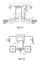
- FIG. 6 a illustrates RF system 600 according to an embodiment of the present invention.
- System 600 includes RF transceiver 602 coupled to antenna 612 via embodiment reflection measurement circuit 604 and tunable matching network 606 .
- the power measurement output of reflection measurement circuit 604 is coupled to A/D converter 608 , the output of which is coupled to controller 610 .
- controller 610 adjusts tunable matching network 606 according to the digitized output of A/D converter 608 .
- controller 610 adjusts tunable matching network 606 until the measured it mismatch in impedance falls below a predetermined threshold in some embodiments.
- controller 610 may be implemented, for example, using a processor, microcontroller, or dedicated system logic.
- RF system 600 may be implemented, for example, in the front end of a cellular telephone, wireless local area network transceiver, or other radio frequency system.
- tunable matching network 606 is coupled between RF transceiver 602 and reflection measurement circuit 604 , as shown in FIG. 6 b with respect to system 620 .
- FIG. 6 c illustrates embodiment radar system 650 according to another embodiment of the present invention.
- System 650 includes radar transceiver 652 coupled to antenna 612 via embodiment reflection measurement circuit 604 .
- the output of the reflection measurement circuit 604 is coupled to the controller 610 via analog to digital converter 608 .
- reflection measurement circuit 604 measures an incident signal from antenna 612 that may represent a reflected radar pulse.
- System 650 may be used, for example, a radar system such as automotive or proximity radar systems.
- Reflection measurement circuit 604 may be implemented, for example, using the embodiments of FIG. 4 c and/or 4 d .
- Other example systems that may utilize embodiment reflection measurement circuits include power monitoring in planar inverted F antenna (PIFA) feed-point tuners.
- PIFA planar inverted F antenna
- FIGS. 6 a - c are just three examples of the many embodiment systems that may be implemented using embodiment of reflection measurement circuits.
- FIG. 7 a illustrates a block diagram 700 of a method of using an embodiment coupler.
- step 702 the amplitudes of Vv and Vi corresponding to the outputs of ports 4 and 5 illustrated in FIG. 1 a are monitored.
- step 704 the sum of Vv and Vi is determined, for example, using a resistive summing network such at that shown in FIG. 4 a .
- a capacitive summing network may be used, and or summing network including impedances that have various real and/or reactive components. In further embodiments, this summing may be performed in the digital domain.
- step 706 a magnitude of a reflection between a source and load impedance is determined based on the sum of Vv and Vi.
- the amplitude of the sum of Vv and Vi is proportional to the magnitude of the measured reflection. The sum of the amplitude may be measured, for example, using an RF power detector.
- FIG. 7 b illustrates a block diagram 720 of a method of using an embodiment coupler to measure incident and reflected waves.
- step 722 the amplitudes of Vv and Vi corresponding to the outputs of ports 4 and 5 illustrated in FIG. 1 a are monitored.
- step 724 the sum of Vv and Vi is determined, for example, using a resistive summing network such at that shown in FIG. 4 a .
- the amplitude of the sum is proportional to a magnitude of a wave propagating in a first direction.
- the difference between Vv and Vi is determined, such that the amplitude of the difference is proportional to a magnitude of a wave propagating in a second direction opposite the first direction. This difference may be determined, for example, by using the circuit described with respect to FIGS. 4 b and 4 c.
- a capacitive summing network may be used, and or summing network including impedances that have various real and/or reactive components. In further embodiments, this summing may be performed in the digital domain.
- a magnitude of a reflection between a source and load impedance is determined based on the sum of Vv and Vi. In some embodiments, the amplitude of the sum of Vv and Vi is proportional to the magnitude of the measured reflection. The sum of the amplitude may be measured, for example, using an RF power detector.
- FIG. 8 a illustrates an embodiment coupler 800 that is similar to the coupler shown in FIG. 1 a , with the addition of a capacitive divider formed by capacitors C 5 and C 6 that may be coupled to the primary winding of transformer X 1 .
- V vQ is in-phase with the voltage V RF such that voltage V vQ at port 5 a and V i at port 5 has a 90 degree phase difference in matched conditions.
- FIG. 8 b illustrates a reflection measurement system using coupler 800 , phase detector 14 and RF power detectors 12 and 13 .
- output 802 of phase detector 14 has a zero and/or minimum output in matched conditions that does not depend on the amplitude of the RF signal at the source or load ports of coupler 800 .
- matched conditions may be recognized without calibrating out the effect of the amplitude of signals present at the source and load ports of coupler 800 .
- a circuit in accordance with an embodiment, includes a magnetic transformer having a first winding coupled between a first signal node and a second signal node, and a second winding coupled between a first reference node and a current measurement node.
- a phase shift network is coupled between the second node and a voltage measurement node, and the circuit is configured to indicate an impedance matching condition based on an amplitude difference and a phase difference between the voltage measurement node and the current measurement node.
- the first signal node may be configured to be coupled to an RF signal source
- the second signal node may be configured to be coupled to an RF load
- the circuit includes RF signal source and the RF load.
- the phase shift network is coupled to the second signal node via a tapped connection on the first winding and/or the phase shift network is configured to provide a 90° phase shift.
- the phase shift network may include a capacitor coupled between the second signal node and the voltage measurement node, and a resistor coupled between the voltage measurement node and a second reference node.
- the first reference node and the second reference node are ground nodes.
- the circuit further includes a detection circuit coupled to the voltage measurement node and the current measurement node.
- the detection circuit may include an RF power detector having an input coupled to the voltage measurement node and the current measurement node.
- the detection circuit includes a first impedance coupled between the current measurement node and a sensing node, and a second impedance coupled between the voltage measurement node and the sensing node.
- An RF power detector may be coupled to the sensing node.
- the first impedance includes a first resistor and the second impedance includes a second resistor.
- the first impedance includes a first capacitor and the second impedance includes a second capacitor.
- the detection circuit may be configured to indicate an impedance match between a reference impedance coupled to the first node and a load impedance coupled to the second node when an output of the RF power detector indicates a minimum power level.
- the detection circuit includes a first RF power detector coupled to the current measurement node, a second RF power detector coupled to the voltage measurement node, and a mixer having a first input coupled to the current measurement node, and second input coupled to the voltage measurement node.
- the circuit may further include a capacitive divider having an input coupled to the first signal node, a first RF power detector coupled to the current measurement node, a second RF power detector coupled to the voltage measurement node, and a mixer having a first input coupled to an output of the capacitive divider network, and second input coupled to the current measurement node.
- a method of operating a reflection measurement circuit includes the steps of monitoring and measuring.
- the reflection measurement circuit includes a magnetic transformer and a phase shift network.
- the magnetic transformer has a first winding coupled between a first signal node and a second signal node and a second winding coupled between a first reference node and a current measurement node, and the phase shift network is coupled between the load node and a voltage measurement node.
- the step of monitoring includes monitoring amplitudes of the voltage measurement node and the current measurement node
- the step of measuring includes measuring a reflection between a first impedance coupled to the first signal node and a second impedance coupled to the second signal node based on the monitoring.
- the method further includes determining an impedance mismatch based on the measured reflection.
- the step of measuring the reflection may include adding a signal at the voltage measurement node to a signal at the current measurement node to form a summed signal, such that an amplitude of the summed signal is proportional to a reflection coefficient describing a reflection from the load impedance to the source impedance.
- the method further includes measuring the amplitude of the summed signal using a power detector, and may further include measuring an amplitude of the current measurement node using a first power detector, and measuring an amplitude of the voltage measurement node using a second power detector.
- the method also includes determining a phase difference between the current measurement node and the voltage measurement node. Determining the phase difference may include, for example, using a phase detector having inputs coupled to the current measurement node and the voltage measurement node.
- the method further includes measuring a wave in a first direction, which includes adding a signal at the voltage measurement node to a signal at the current measurement node to form a summed signal, and measuring a wave in a second direction, which includes subtracting a signal at the current measurement node to a signal at the voltage measurement node to form a subtracted signal.
- a semiconductor circuit includes a semiconductor substrate, a magnetic transformer, and a phase shift network.
- the magnetic transformer includes a primary metallization trace disposed on the semiconductor substrate, and a secondary metallization trace disposed adjacent to the primary metallization trace.
- a first end of the primary metallization trace is configured to be coupled to a reference impedance and a second end of the primary metallization trace is configured to be coupled to a load impedance, and the first end of the secondary metallization trace is configured to be coupled to a first reference voltage node and a second end is configured to be coupled to a current measurement node.
- the phase shift network has a first node coupled to the second end of the first of metallization trace and a voltage measurement node.
- the phase shift network includes a capacitor coupled between the second of the primary metallization trace and the voltage measurement node, and a resistor coupled between the voltage sensing node and a second reference voltage node.
- the capacitor may be implemented using a metallization area capacitively coupled to the primary metallization trace, and the resistor may be implemented using a metal resistor.
- the semiconductor circuit further includes an RF power detector having an input coupled to the voltage measurement node and the current measurement node.
- the semiconductor circuit also includes a first impedance coupled between the current measurement node and a sensing node, and a second impedance coupled between the voltage measurement node and the sensing node.
- the first impedance may include a first resistor and the second impedance may include a second resistor.
- the first impedance may include a first capacitor and the second impedance may include a second capacitor.
- the semiconductor circuit may also include an RF power detector having an input coupled to the sensing node.
- Advantages of embodiments of the present invention include the ability to implement a directional coupler and/or impedance mismatch measurement device that has a very low insertion loss, a small form factor suitable for integration on-chip, and the ability to operate at low RF frequencies, for example, between 500 MHz and 3 GHz.
Landscapes
- Physics & Mathematics (AREA)
- Condensed Matter Physics & Semiconductors (AREA)
- General Physics & Mathematics (AREA)
- Measurement Of Resistance Or Impedance (AREA)
- Transmitters (AREA)
Abstract
Description
where ZL represents load impedance, Z0 represents the characteristic impedances, which may be 50 ΩOhms, and Γ0 represents the reflection coefficient. In some embodiments, a magnetic transformer generates a voltage proportional to an RF current and an RC network generates voltage proportional to an RF voltage. In some embodiments, the coupler is constructed such that amplitudes and phases of the voltage proportional to the RF current and the voltage proportional to the RF voltage are 180 degrees out of phase and have the same amplitude when there is no reflection in the RF signal path.
V i =−jω·k√{square root over (L P L s)}·I RF, (1)
where Lp and Ls are the self-inductance of primary and secondary windings of transformer X1, and k is a coupling factor between primary and secondary windings of X1.
When the cut-off frequency of the RC network is well above the operating frequency range of the coupler, namely
equation (2) may be approximated as follows:
V v ≈jωR 1 C 1 ·V RF. (4)
where Z0 is a reference impedance. In some embodiments, Z0 may be set to the characteristic impedance of the system, which may be, for example, 50Ω, or another impedance. If load impedance ZL for the RF signal at
V v +V i=0 (6a)
because |Vv|=|Vi| and ∠Vv−∠Vi=180°. In the case of an impedance mismatch, for example, when ZL≠Z0,
V v +V i≠0. (6b)
Consequently, voltages Vi and Vv at
Under this condition, voltages Vi and Vv at
where VRF + and IRF + are incident voltage and current, VRF − and IRF − are the reflected voltage and current. Substituting (7) and (8) into (1) and (4) results in:
According to (5):
Substituting (11) into (9) results in:
V i =−jω·R 1 C 1 ·V RF + +jω·R 1 C 1 ·V RF − (12)
Finally, by adding and subtracting voltages, as shown in equations (10) and (12), reflected and incident power in the RF line can be monitored as follows:
V v +V i=2jω·R 1 C 1 ·V RF −
V v −V i=2jω·R 1 C 1 ·V RF +
Claims (34)
Priority Applications (4)
| Application Number | Priority Date | Filing Date | Title |
|---|---|---|---|
| US13/931,092 US9535140B2 (en) | 2013-06-28 | 2013-06-28 | System and method for a transformer and a phase-shift network |
| DE102014109003.9A DE102014109003B4 (en) | 2013-06-28 | 2014-06-26 | Circuit and method for a transformer and a phase shifter network |
| CN201410302990.4A CN104251939B (en) | 2013-06-28 | 2014-06-27 | For transformer and the system and method for phase-shift network |
| KR1020140079561A KR101698240B1 (en) | 2013-06-28 | 2014-06-27 | System and method for a transformer and a phase-shift network |
Applications Claiming Priority (1)
| Application Number | Priority Date | Filing Date | Title |
|---|---|---|---|
| US13/931,092 US9535140B2 (en) | 2013-06-28 | 2013-06-28 | System and method for a transformer and a phase-shift network |
Publications (2)
| Publication Number | Publication Date |
|---|---|
| US20150002146A1 US20150002146A1 (en) | 2015-01-01 |
| US9535140B2 true US9535140B2 (en) | 2017-01-03 |
Family
ID=52017528
Family Applications (1)
| Application Number | Title | Priority Date | Filing Date |
|---|---|---|---|
| US13/931,092 Active 2035-01-05 US9535140B2 (en) | 2013-06-28 | 2013-06-28 | System and method for a transformer and a phase-shift network |
Country Status (4)
| Country | Link |
|---|---|
| US (1) | US9535140B2 (en) |
| KR (1) | KR101698240B1 (en) |
| CN (1) | CN104251939B (en) |
| DE (1) | DE102014109003B4 (en) |
Families Citing this family (8)
| Publication number | Priority date | Publication date | Assignee | Title |
|---|---|---|---|---|
| US9319006B2 (en) | 2013-10-01 | 2016-04-19 | Infineon Technologies Ag | System and method for a radio frequency coupler |
| US9608305B2 (en) | 2014-01-14 | 2017-03-28 | Infineon Technologies Ag | System and method for a directional coupler with a combining circuit |
| US9322858B2 (en) | 2014-02-04 | 2016-04-26 | Infineon Technologies Austria Ag | System and method for a phase detector |
| US9866260B2 (en) | 2014-09-12 | 2018-01-09 | Infineon Technologies Ag | System and method for a directional coupler module |
| GB201503181D0 (en) * | 2015-02-25 | 2015-04-08 | Cellpath Ltd | Histology cassette stack |
| US9947985B2 (en) | 2015-07-20 | 2018-04-17 | Infineon Technologies Ag | System and method for a directional coupler |
| US10523254B2 (en) * | 2017-07-20 | 2019-12-31 | Qualcomm Incorporated | Mixer S11 control via sum component termination |
| CN111766552B (en) * | 2020-07-06 | 2022-12-27 | 河北工业大学 | Automatic impedance matching device and method for magnetic characteristic measurement system |
Citations (27)
| Publication number | Priority date | Publication date | Assignee | Title |
|---|---|---|---|---|
| US4205282A (en) * | 1978-08-21 | 1980-05-27 | Westinghouse Electric Corp. | Phase shifting circuit element |
| US4951009A (en) | 1989-08-11 | 1990-08-21 | Applied Materials, Inc. | Tuning method and control system for automatic matching network |
| US4967159A (en) * | 1989-02-23 | 1990-10-30 | Abbott Laboratories | Self-balancing reflectometer |
| WO1995017683A1 (en) | 1993-12-21 | 1995-06-29 | Siemens Aktiengesellschaft | Automatic impedance adapter for a h.f. emitter or receiver in a nuclear spin tomography installation and process for operating the device |
| US5585766A (en) | 1994-10-27 | 1996-12-17 | Applied Materials, Inc. | Electrically tuned matching networks using adjustable inductance elements |
| CN1298105A (en) | 1999-11-25 | 2001-06-06 | 株式会社爱德万测试 | Network analytical instrument, network analytical method and recording media |
| US6600307B2 (en) | 2000-03-02 | 2003-07-29 | Sarnoff Corporation | Method and apparatus for measuring true transmitted power using a broadband dual directional coupler |
| US6768318B2 (en) | 2001-02-22 | 2004-07-27 | Texas Instruments Incorporated | Signal conditioning circuit for resistive sensors |
| CN1799033A (en) | 2003-06-03 | 2006-07-05 | 安捷伦科技有限公司 | A network analyzing method and a network analyzing apparatus |
| CN1938595A (en) | 2004-03-26 | 2007-03-28 | 株式会社爱德万测试 | Network analyzer, transmission tracking measuring method, network analyzing method, program, and recording medium |
| US20090098840A1 (en) * | 2007-10-11 | 2009-04-16 | Nokia Corporation | Apparatus and method for measuring the level of RF signals, and a transmitter including a wide band measurement circuit |
| US7576626B2 (en) | 2006-09-08 | 2009-08-18 | Stmicroelectronics Ltd. | Directional couplers for RF power detection |
| US7629795B2 (en) | 2007-07-30 | 2009-12-08 | John D. Terleski | Vector impedance measurement system and method of using same |
| US20100019983A1 (en) * | 2008-07-23 | 2010-01-28 | Stmicroelectronics (Tours) Sas | Detection of the value of an impedance of a radiofrequency system |
| US20100079218A1 (en) * | 2008-09-26 | 2010-04-01 | Albag Yehezkel | Chockless power coupler |
| WO2010098909A1 (en) | 2009-02-24 | 2010-09-02 | Osteomed L.P. | Multiple bone fusion plate |
| US20110102246A1 (en) * | 2009-11-02 | 2011-05-05 | Moulton Grant E | Noise-canceling down-converting detector |
| US20110313698A1 (en) | 2009-02-25 | 2011-12-22 | Panasonic Corporation | Voltage polarity determination circuit and charge amount measurement circuit |
| US20120001693A1 (en) | 2007-07-11 | 2012-01-05 | Rahul Magoon | Power amplifier amplitude modulator system and method |
| US20120232471A1 (en) * | 2011-03-08 | 2012-09-13 | Baxter Healthcare S.A. | Non-invasive radio frequency medical fluid level and volume detection system and method |
| US8326234B2 (en) | 2010-02-12 | 2012-12-04 | Infineon Technologies Ag | High frequency switching circuit and method for determining a power of a high frequency signal |
| KR20130070442A (en) | 2011-12-19 | 2013-06-27 | 엘지이노텍 주식회사 | Apparatus and method for matching impedence |
| US8606198B1 (en) * | 2012-07-20 | 2013-12-10 | Triquint Semiconductor, Inc. | Directional coupler architecture for radio frequency power amplifier with complex load |
| US20130343107A1 (en) * | 2012-06-25 | 2013-12-26 | Eta Devices, Inc. | Transmission-Line Resistance Compression Networks And Related Techniques |
| US20140155003A1 (en) * | 2012-01-05 | 2014-06-05 | Panasonic Corporation | Quadrature hybrid coupler, amplifier, and wireless communication device |
| US8798546B2 (en) * | 2011-01-31 | 2014-08-05 | Telcordia Technologies, Inc. | Directional filter for separating closely spaced channels in an HF transceiver |
| US9061641B2 (en) * | 2011-01-07 | 2015-06-23 | Iee International Electronics & Engineering S.A. | Capacitive sensor including resonant network |
Family Cites Families (1)
| Publication number | Priority date | Publication date | Assignee | Title |
|---|---|---|---|---|
| WO2010098090A1 (en) * | 2009-02-25 | 2010-09-02 | パナソニック株式会社 | Voltage polarity discrimination circuit and electrical load measuring circuit |
-
2013
- 2013-06-28 US US13/931,092 patent/US9535140B2/en active Active
-
2014
- 2014-06-26 DE DE102014109003.9A patent/DE102014109003B4/en active Active
- 2014-06-27 KR KR1020140079561A patent/KR101698240B1/en active IP Right Grant
- 2014-06-27 CN CN201410302990.4A patent/CN104251939B/en active Active
Patent Citations (33)
| Publication number | Priority date | Publication date | Assignee | Title |
|---|---|---|---|---|
| US4205282A (en) * | 1978-08-21 | 1980-05-27 | Westinghouse Electric Corp. | Phase shifting circuit element |
| US4967159A (en) * | 1989-02-23 | 1990-10-30 | Abbott Laboratories | Self-balancing reflectometer |
| US4951009A (en) | 1989-08-11 | 1990-08-21 | Applied Materials, Inc. | Tuning method and control system for automatic matching network |
| DE69023417T2 (en) | 1989-08-11 | 1996-05-15 | Applied Materials Inc | Adaptation circuit and method for their use. |
| WO1995017683A1 (en) | 1993-12-21 | 1995-06-29 | Siemens Aktiengesellschaft | Automatic impedance adapter for a h.f. emitter or receiver in a nuclear spin tomography installation and process for operating the device |
| US5777475A (en) | 1993-12-21 | 1998-07-07 | Siemens Aktiengesellschaft | Automatic impedance adapter for a H.F. emitter or receiver in a nuclear spin tomography installation and process for operating the device |
| US5585766A (en) | 1994-10-27 | 1996-12-17 | Applied Materials, Inc. | Electrically tuned matching networks using adjustable inductance elements |
| US6496785B1 (en) | 1999-11-25 | 2002-12-17 | Advantest Corporation | Network analyzer, network analytical method and recording medium |
| CN1298105A (en) | 1999-11-25 | 2001-06-06 | 株式会社爱德万测试 | Network analytical instrument, network analytical method and recording media |
| US6600307B2 (en) | 2000-03-02 | 2003-07-29 | Sarnoff Corporation | Method and apparatus for measuring true transmitted power using a broadband dual directional coupler |
| US6768318B2 (en) | 2001-02-22 | 2004-07-27 | Texas Instruments Incorporated | Signal conditioning circuit for resistive sensors |
| CN1799033A (en) | 2003-06-03 | 2006-07-05 | 安捷伦科技有限公司 | A network analyzing method and a network analyzing apparatus |
| CN1938595A (en) | 2004-03-26 | 2007-03-28 | 株式会社爱德万测试 | Network analyzer, transmission tracking measuring method, network analyzing method, program, and recording medium |
| US20070285108A1 (en) | 2004-03-26 | 2007-12-13 | Advantest Corporation | Network Analyzer, Transmission Tracking Error Measuring Method, Network Analyzing Method, Program, And Recording Medium |
| US7576626B2 (en) | 2006-09-08 | 2009-08-18 | Stmicroelectronics Ltd. | Directional couplers for RF power detection |
| US20120001693A1 (en) | 2007-07-11 | 2012-01-05 | Rahul Magoon | Power amplifier amplitude modulator system and method |
| US7629795B2 (en) | 2007-07-30 | 2009-12-08 | John D. Terleski | Vector impedance measurement system and method of using same |
| US20090098840A1 (en) * | 2007-10-11 | 2009-04-16 | Nokia Corporation | Apparatus and method for measuring the level of RF signals, and a transmitter including a wide band measurement circuit |
| US20100019983A1 (en) * | 2008-07-23 | 2010-01-28 | Stmicroelectronics (Tours) Sas | Detection of the value of an impedance of a radiofrequency system |
| US20100079218A1 (en) * | 2008-09-26 | 2010-04-01 | Albag Yehezkel | Chockless power coupler |
| CN101953018A (en) | 2008-09-26 | 2011-01-19 | 埃克斯腾网络有限公司 | Chockless power coupler |
| US8149070B2 (en) * | 2008-09-26 | 2012-04-03 | Albag Yehezkel | Chockless power coupler |
| WO2010098909A1 (en) | 2009-02-24 | 2010-09-02 | Osteomed L.P. | Multiple bone fusion plate |
| US20110313698A1 (en) | 2009-02-25 | 2011-12-22 | Panasonic Corporation | Voltage polarity determination circuit and charge amount measurement circuit |
| US20110102246A1 (en) * | 2009-11-02 | 2011-05-05 | Moulton Grant E | Noise-canceling down-converting detector |
| US8326234B2 (en) | 2010-02-12 | 2012-12-04 | Infineon Technologies Ag | High frequency switching circuit and method for determining a power of a high frequency signal |
| US9061641B2 (en) * | 2011-01-07 | 2015-06-23 | Iee International Electronics & Engineering S.A. | Capacitive sensor including resonant network |
| US8798546B2 (en) * | 2011-01-31 | 2014-08-05 | Telcordia Technologies, Inc. | Directional filter for separating closely spaced channels in an HF transceiver |
| US20120232471A1 (en) * | 2011-03-08 | 2012-09-13 | Baxter Healthcare S.A. | Non-invasive radio frequency medical fluid level and volume detection system and method |
| KR20130070442A (en) | 2011-12-19 | 2013-06-27 | 엘지이노텍 주식회사 | Apparatus and method for matching impedence |
| US20140155003A1 (en) * | 2012-01-05 | 2014-06-05 | Panasonic Corporation | Quadrature hybrid coupler, amplifier, and wireless communication device |
| US20130343107A1 (en) * | 2012-06-25 | 2013-12-26 | Eta Devices, Inc. | Transmission-Line Resistance Compression Networks And Related Techniques |
| US8606198B1 (en) * | 2012-07-20 | 2013-12-10 | Triquint Semiconductor, Inc. | Directional coupler architecture for radio frequency power amplifier with complex load |
Non-Patent Citations (1)
| Title |
|---|
| Bahl, "Chapter 12 Lumped-Element Circuits," Artechhouse, Jun. 7, 2003, 42 pages. |
Also Published As
| Publication number | Publication date |
|---|---|
| CN104251939A (en) | 2014-12-31 |
| KR101698240B1 (en) | 2017-01-19 |
| US20150002146A1 (en) | 2015-01-01 |
| DE102014109003A1 (en) | 2014-12-31 |
| DE102014109003B4 (en) | 2018-04-12 |
| KR20150002524A (en) | 2015-01-07 |
| CN104251939B (en) | 2017-12-15 |
Similar Documents
| Publication | Publication Date | Title |
|---|---|---|
| US9535140B2 (en) | System and method for a transformer and a phase-shift network | |
| US9608305B2 (en) | System and method for a directional coupler with a combining circuit | |
| KR101855836B1 (en) | System and method for a directional coupler | |
| US7479864B2 (en) | Total fluid conductivity sensor system and method | |
| US9322858B2 (en) | System and method for a phase detector | |
| US8543071B2 (en) | Radiofrequency emission or reception chain with automatic impedance adaptation, and corresponding method | |
| US9804195B2 (en) | HF measuring probe contacting assembly | |
| US8907702B1 (en) | System and method for a phase detector | |
| Zhang et al. | A novel structure of high directivity broadband microstrip coupler | |
| Eroglu et al. | Novel broadband multilayer microstrip directional couplers | |
| Law et al. | Rf probe technology for the next generation of technological plasmas | |
| RU2499274C1 (en) | Device to determine noise parameters of microwave quadripole | |
| CN106199211A (en) | A kind of broadband microwave parameter and load measuring device | |
| Pečovsky et al. | Instrumentation amplifier for ultra-wideband applications | |
| WO2012089253A1 (en) | A waveguide based five or six port circuit | |
| Letavin et al. | Determination of the electrodynamic properties of the material and their subsequent use for the realization of a miniature microstrip coupler device | |
| RU2498333C1 (en) | Device for determining noise parametres of uhf four-pole | |
| Raab | Model for the low-frequency performance of ferrite-loaded balun transformers | |
| Hung et al. | Asymmetrical balun design with tunable bandwidth and transmission zero | |
| Liu | Design and implementation of a broadband diode power sensor covering 0.01 GHz to 50GHz | |
| WO2020117101A1 (en) | Diode detector of microwave signal power | |
| Biernacki et al. | RF transformer as a directional coupler with arbitrary load | |
| Minerva | Comments on" Differentially Driven Symmetric Microstrip Inductors" | |
| CN103869177A (en) | Radio frequency measuring device |
Legal Events
| Date | Code | Title | Description |
|---|---|---|---|
| AS | Assignment |
Owner name: INFINEON TECHNOLOGIES AG, GERMANY Free format text: ASSIGNMENT OF ASSIGNORS INTEREST;ASSIGNORS:SOLOMKO, VALENTYN;BAKALSKI, WINFRIED;REEL/FRAME:030725/0356 Effective date: 20130628 |
|
| FEPP | Fee payment procedure |
Free format text: PAYOR NUMBER ASSIGNED (ORIGINAL EVENT CODE: ASPN); ENTITY STATUS OF PATENT OWNER: LARGE ENTITY |
|
| STCF | Information on status: patent grant |
Free format text: PATENTED CASE |
|
| MAFP | Maintenance fee payment |
Free format text: PAYMENT OF MAINTENANCE FEE, 4TH YEAR, LARGE ENTITY (ORIGINAL EVENT CODE: M1551); ENTITY STATUS OF PATENT OWNER: LARGE ENTITY Year of fee payment: 4 |