US9530855B2 - Semiconductor device with polycrystalline silicon film - Google Patents
Semiconductor device with polycrystalline silicon film Download PDFInfo
- Publication number
- US9530855B2 US9530855B2 US14/792,879 US201514792879A US9530855B2 US 9530855 B2 US9530855 B2 US 9530855B2 US 201514792879 A US201514792879 A US 201514792879A US 9530855 B2 US9530855 B2 US 9530855B2
- Authority
- US
- United States
- Prior art keywords
- film
- polycrystalline silicon
- silicon film
- semiconductor device
- gate electrode
- Prior art date
- Legal status (The legal status is an assumption and is not a legal conclusion. Google has not performed a legal analysis and makes no representation as to the accuracy of the status listed.)
- Active
Links
Images


Classifications
-
- H01L29/4925—
-
- H—ELECTRICITY
- H10—SEMICONDUCTOR DEVICES; ELECTRIC SOLID-STATE DEVICES NOT OTHERWISE PROVIDED FOR
- H10D—INORGANIC ELECTRIC SEMICONDUCTOR DEVICES
- H10D64/00—Electrodes of devices having potential barriers
- H10D64/60—Electrodes characterised by their materials
- H10D64/66—Electrodes having a conductor capacitively coupled to a semiconductor by an insulator, e.g. MIS electrodes
- H10D64/661—Electrodes having a conductor capacitively coupled to a semiconductor by an insulator, e.g. MIS electrodes the conductor comprising a layer of silicon contacting the insulator, e.g. polysilicon having vertical doping variation
- H10D64/662—Electrodes having a conductor capacitively coupled to a semiconductor by an insulator, e.g. MIS electrodes the conductor comprising a layer of silicon contacting the insulator, e.g. polysilicon having vertical doping variation the conductor further comprising additional layers, e.g. multiple silicon layers having different crystal structures
-
- H01L21/28273—
-
- H01L27/11541—
-
- H01L29/42324—
-
- H01L29/7885—
-
- H—ELECTRICITY
- H10—SEMICONDUCTOR DEVICES; ELECTRIC SOLID-STATE DEVICES NOT OTHERWISE PROVIDED FOR
- H10B—ELECTRONIC MEMORY DEVICES
- H10B41/00—Electrically erasable-and-programmable ROM [EEPROM] devices comprising floating gates
- H10B41/40—Electrically erasable-and-programmable ROM [EEPROM] devices comprising floating gates characterised by the peripheral circuit region
- H10B41/42—Simultaneous manufacture of periphery and memory cells
- H10B41/43—Simultaneous manufacture of periphery and memory cells comprising only one type of peripheral transistor
- H10B41/47—Simultaneous manufacture of periphery and memory cells comprising only one type of peripheral transistor with a floating-gate layer also being used as part of the peripheral transistor
-
- H—ELECTRICITY
- H10—SEMICONDUCTOR DEVICES; ELECTRIC SOLID-STATE DEVICES NOT OTHERWISE PROVIDED FOR
- H10D—INORGANIC ELECTRIC SEMICONDUCTOR DEVICES
- H10D30/00—Field-effect transistors [FET]
- H10D30/60—Insulated-gate field-effect transistors [IGFET]
- H10D30/68—Floating-gate IGFETs
- H10D30/681—Floating-gate IGFETs having only two programming levels
- H10D30/684—Floating-gate IGFETs having only two programming levels programmed by hot carrier injection
- H10D30/685—Floating-gate IGFETs having only two programming levels programmed by hot carrier injection from the channel
-
- H—ELECTRICITY
- H10—SEMICONDUCTOR DEVICES; ELECTRIC SOLID-STATE DEVICES NOT OTHERWISE PROVIDED FOR
- H10D—INORGANIC ELECTRIC SEMICONDUCTOR DEVICES
- H10D30/00—Field-effect transistors [FET]
- H10D30/60—Insulated-gate field-effect transistors [IGFET]
- H10D30/68—Floating-gate IGFETs
- H10D30/6891—Floating-gate IGFETs characterised by the shapes, relative sizes or dispositions of the floating gate electrode
-
- H—ELECTRICITY
- H10—SEMICONDUCTOR DEVICES; ELECTRIC SOLID-STATE DEVICES NOT OTHERWISE PROVIDED FOR
- H10D—INORGANIC ELECTRIC SEMICONDUCTOR DEVICES
- H10D64/00—Electrodes of devices having potential barriers
- H10D64/01—Manufacture or treatment
- H10D64/031—Manufacture or treatment of data-storage electrodes
- H10D64/035—Manufacture or treatment of data-storage electrodes comprising conductor-insulator-conductor-insulator-semiconductor structures
-
- H01L23/485—
-
- H01L2924/00—
-
- H01L2924/0002—
-
- H—ELECTRICITY
- H10—SEMICONDUCTOR DEVICES; ELECTRIC SOLID-STATE DEVICES NOT OTHERWISE PROVIDED FOR
- H10W—GENERIC PACKAGES, INTERCONNECTIONS, CONNECTORS OR OTHER CONSTRUCTIONAL DETAILS OF DEVICES COVERED BY CLASS H10
- H10W20/00—Interconnections in chips, wafers or substrates
- H10W20/40—Interconnections external to wafers or substrates, e.g. back-end-of-line [BEOL] metallisations or vias connecting to gate electrodes
Definitions
- Embodiments described herein relates to a semiconductor device.
- a MOS transistor is a basic configuration unit of an integrated circuit (LSI) included in a semiconductor device, and one of the most important aspects of performance of the MOS transistor is reliability of its gate insulating film.
- Reliability of the gate insulating film is known to depend on concentration of hydrogen included in the gate insulating film.
- LSI integrated circuit
- a passivation film configured from a silicon nitride film to be provided in a layer above a memory structure. This silicon nitride film contains a lot of hydrogen. Problems sometimes occur when this hydrogen is diffused to the gate insulating film.
- One such problem is that reliability of the gate insulating film degrades and a threshold voltage of the transistor fluctuates.
- a hydrogen block layer which is for avoiding diffusion of hydrogen and avoiding mixing of hydrogen in the gate insulating film, is provided temporarily midway through a manufacturing process.
- the hydrogen block layer of this conventional technology is provided only during the manufacturing process and is removed by etching in a final product, and is formed with a large film thickness of as much as 800 nm.
- the hydrogen block layer ends up being removed in the final product, it cannot suppress diffusion of hydrogen after shipment.
- FIG. 1 is a cross-sectional view explaining a structure of a nonvolatile semiconductor memory device according to an embodiment.
- FIG. 2 is a graph explaining an advantage of the structure of the embodiment.
- FIG. 3 is a graph explaining an advantage of the structure of the embodiment.
- FIG. 4 is a graph explaining an advantage of the structure of the embodiment.
- FIG. 5 is a process drawing explaining a method of manufacturing a nonvolatile semiconductor memory device according to the embodiment.
- FIG. 6 is a process drawing explaining the method of manufacturing a nonvolatile semiconductor memory device according to the embodiment.
- FIG. 7 is a process drawing explaining the method of manufacturing a nonvolatile semiconductor memory device according to the embodiment.
- FIG. 8 is a process drawing explaining the method of manufacturing a nonvolatile semiconductor memory device according to the embodiment.
- FIG. 9 is a process drawing explaining the method of manufacturing a nonvolatile semiconductor memory device according to the embodiment.
- FIG. 10 is a process drawing explaining the method of manufacturing a nonvolatile semiconductor memory device according to the embodiment.
- FIG. 11 is a process drawing explaining the method of manufacturing a nonvolatile semiconductor memory device according to the embodiment.
- FIG. 12 is a process drawing explaining the method of manufacturing a nonvolatile semiconductor memory device according to the embodiment.
- FIG. 13 is a process drawing explaining the method of manufacturing a nonvolatile semiconductor memory device according to the embodiment.
- FIG. 14 is a process drawing explaining the method of manufacturing a nonvolatile semiconductor memory device according to the embodiment.
- FIG. 15 is a process drawing explaining the method of manufacturing a nonvolatile semiconductor memory device according to the embodiment.
- a semiconductor device comprises: a gate insulating film provided on a surface of a channel layer; a gate electrode provided on an upper surface of the gate insulating film; and a diffusion layer provided in the channel layer. Furthermore, this semiconductor device comprises: a polycrystalline silicon film provided so as to cover a surface of the gate electrode and the diffusion layer; and an inter-layer insulating film provided so as to cover the gate electrode and the polycrystalline silicon film.
- FIG. 1 is a schematic cross-sectional view of a memory cell region MA and a peripheral transistor region TA of a nonvolatile semiconductor memory device according to the present embodiment. Dimensions of configuration elements illustrated are sometimes different from an actual scale of each of the configuration elements.
- a flash memory cell is exemplified as a memory transistor, and a semiconductor device in which a flash memory cell transistor and a peripheral transistor are both mounted, is exemplified.
- the present invention is not limited to this configuration, and may be applied to a semiconductor device including a transistor in general.
- This nonvolatile semiconductor memory device comprises: a memory cell transistor MC formed in the memory cell region MA; and a peripheral transistor Tr formed in the peripheral transistor region TA and controlling the memory cell transistor MC.
- the peripheral transistor Tr is, for example, a transistor included in the likes of a row decoder, a column decoder, and a voltage generating circuit, acting as a peripheral circuit.
- the memory cell transistor MC comprises: a P type silicon substrate 11 ; and a gate electrode 18 a formed on the silicon substrate 11 via a gate insulating film 14 a configured from a silicon oxide film, for example.
- a NAND type flash memory a plurality of the memory transistors MC of the kind shown in this FIG. 1 are connected in series to configure a memory string.
- select transistors (not illustrated) are connected to both ends of this memory string to configure a NAND cell unit.
- the gate electrode 18 a is configured from: a floating gate (FG) 15 a configured from polycrystalline silicon doped with an impurity such as phosphorus (P), for example; an inter-gate insulating film 16 a deposited on the floating gate 15 a ; and a control gate 17 a configured from polycrystalline silicon, for example, and deposited on the floating gate 15 a via the inter-gate insulating film 16 a.
- FG floating gate
- P phosphorus
- the gate insulating film 14 a is configured by a silicon oxide film (SiOx) having a film thickness of about 8 nm, for example.
- the inter-gate insulating film 16 a is also configured from a silicon oxide film (SiOx), for example, having a film thickness of about 8 to 20 nm.
- a sidewall film 19 a configured from a silicon oxide film, for example.
- a P type well 11 a formed in a surface layer portion of the silicon substrate 11 is a P type well 11 a .
- the P type well 11 a functions as a channel layer of the memory transistor MC.
- N type diffusion layers 12 a and 12 a ′ Formed in a surface of this P type well 11 a so as to sandwich the gate electrode 18 a are N type diffusion layers 12 a and 12 a ′.
- the N type diffusion layers 12 a and 12 a ′ act as a source or drain of the memory transistor MC.
- the diffusion layer 12 a is formed by performing ion implantation of an impurity such as phosphorus (P), for example, in a self-aligning manner.
- P phosphorus
- the peripheral transistor Tr comprises: the P type silicon substrate 11 ; a gate insulating film 14 b formed on the P type silicon substrate 11 and configured from a silicon oxide film, for example; and a gate electrode 18 b .
- the gate electrode 18 b is configured from: a lower gate electrode 15 b configured from polycrystalline silicon doped with an impurity such as phosphorus (P), for example; an inter-gate insulating film 16 b deposited on the lower gate electrode 15 b ; and an upper gate electrode 17 b formed on the inter-gate insulating film 16 b .
- the gate insulating film 14 b has a film thickness of about 20 nm to 50 nm, for example, such that a high breakdown strength of about 5 to 30 V, for example, is obtained.
- the inter-gate insulating film 16 b is configured from an identical material to and formed simultaneously to the previously-mentioned inter-gate insulating film 16 a . However, the inter-gate insulating film 16 b comprises an opening close to its central portion in order to connect the lower gate electrode 15 b and the upper gate electrode 17 b.
- a sidewall film 19 b configured from a silicon oxide film (SiO2), for example.
- N type diffusion layers 12 b and 12 b ′ Formed in a surface layer portion of the P type silicon substrate 11 so as to sandwich the gate electrode 18 b are N type diffusion layers 12 b and 12 b ′.
- the N type diffusion layers 12 b and 12 b ′ act as a source or drain of the peripheral transistor Tr.
- the diffusion layers 12 b and 12 b ′ are formed by performing ion implantation of an impurity such as phosphorus (P), for example, in a self-aligning manner.
- P phosphorus
- surfaces of the diffusion layers 12 a , 12 a ′, 12 b , and 12 b ′, and of the gate electrodes 18 a and 18 b may be silicided by depositing a metal film of the likes of nickel thereon and then performing heat treatment, for the purpose of lowering their resistance.
- a liner film 21 and a polycrystalline silicon film 22 are deposited in that order so as to cover the gate electrodes 18 a and 18 b of the memory transistor MC and the peripheral transistor Tr, and the diffusion layers 12 a , 12 a ′, 12 b , and 12 b ′ described above.
- the liner film 21 and the polycrystalline silicon film 22 are formed along an uneven surface that results from the silicon substrate 11 and the gate electrodes 18 a and 18 b .
- the liner film 21 and the polycrystalline silicon film 22 are formed continuously over a plurality of the memory transistors MC in the memory cell region MA, and are formed continuously over a plurality of the peripheral transistors Tr in the peripheral circuit region TA.
- the polycrystalline silicon film 22 is formed having a film thickness of 8 nm or more in a cross section thereof, and so as to have an average particle diameter of 30 nm or less in a plan view thereof, in order to provide a function of preventing diffusion of hydrogen.
- the liner film 21 is configured from an insulating film of the likes of a silicon oxide film (SiOx), for example, and is deposited so as to have a film thickness of about 5 to 20 nm, for example.
- the liner film 21 is formed at least between the diffusion layers 12 a , 12 a ′, 12 b , and 12 b ′ and the polycrystalline silicon film 22 and between the gate electrodes 18 a and 18 b and the polycrystalline silicon film 22 , and has a function of electrically insulating between the two.
- the resistivity of the polycrystalline silicon film 22 is low, and the polycrystalline silicon film 22 and the diffusion layers 12 a , 12 a ′, 12 b , and 12 b ′ contact each other, while the polycrystalline silicon film 22 and the gate electrodes 18 a and 18 b contact each other, there is a risk that the diffusion layers 12 a , 12 a ′, 12 b , and 12 b ′ and the gate electrodes 18 a and 18 b end up being electrically short-circuited.
- the liner film 21 in the above-described way makes it possible for the diffusion layers 12 a , 12 a ′, 12 b , and 12 b ′ and the gate electrodes 18 a and 18 b to be electrically insulated.
- this liner film 21 may also be omitted. That is, in the case that resistivity of the polycrystalline silicon film 22 is sufficiently high, the polycrystalline silicon film 22 may directly contact the diffusion layers 12 a , 12 a ′, 12 b , and 12 b ′ and the gate electrodes 18 a and 18 b.
- the polycrystalline silicon film 22 has a function of suppressing movement of hydrogen diffused from other portions, for example, a later-mentioned passivation film 27 , and thereby preventing hydrogen being absorbed in the gate insulating films 14 a and 14 b and reliability degradation.
- an inter-layer insulating film 23 is deposited so as to cover these liner film 21 and polycrystalline silicon film 22 and bury a gate electrode structure ( 18 a and 18 b ).
- a gate electrode structure 18 a and 18 b
- at contact hole H is formed so as to penetrate these inter-layer insulating film 23 , polycrystalline silicon film 22 , and liner film 21 to reach the diffusion layers 12 a , 12 a ′, 12 b , and 12 b ′ or the gate electrodes 18 a and 18 b .
- Formed in this contact hole H are an isolating insulating film 24 and a contact 25 .
- the isolating insulating film 24 is formed on a sidewall of the contact hole H between the contact 25 and the inter-layer insulating film 23 or the polycrystalline silicon film 22 , with a film thickness of 5 nm or more, for example, and has a function of isolating and insulating the contact 25 and the polycrystalline silicon film 22 . Note that when resistivity of the polycrystalline silicon film 22 is sufficiently high, this isolating insulating film 24 may be omitted.
- a wiring line 26 is formed at upper ends of these plurality of contacts 25 , and this wiring line 26 is connected to an external circuit not illustrated.
- the passivation film 27 is formed on a surface layer portion of the inter-layer insulating film 23 .
- This passivation film 27 includes a silicon nitride film in a part thereof.
- the silicon nitride film contains a lot of hydrogen.
- the hydrogen included in the passivation film 27 separates from the passivation film 27 to diffuse downwards, due to a heat process performed when the passivation film 27 is deposited, a voltage stress during use after shipment, various other kinds of stresses. If such hydrogen is diffused to the gate insulating films 14 a and 14 b , reliability of the gate insulating films 14 a and 14 b degrades.
- the polycrystalline silicon film 22 is formed between the passivation film 27 and the gate insulating films 14 a and 14 b . Therefore, even if hydrogen has diffused from the passivation film 27 , almost all of the hydrogen has its movement suppressed by a dangling bond at an interface of the polycrystalline silicon film 22 , and is prevented from reaching the gate insulating films 14 a and 14 b.
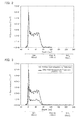
- FIG. 2 is a result of implementing depth direction analysis of hydrogen concentration, on a stacked sample, by a resonance nuclear reaction method.
- the stacked sample has a silicon oxide film (SiO2) of a film thickness of 50 nm deposited on a silicon substrate by a thermal oxidation method, a polycrystalline silicon, film of a film thickness of 100 nm further deposited on the silicon oxide film by a CVD method, and a silicon nitride film (SiN) of a film thickness of 80 nm further deposited on the polycrystalline silicon film by a CVD method.
- the strong signal observed in a region of a surface is a signal resulting from hydrogen adsorbed close to the surface of the stacked sample.
- hydrogen is detected limited to in the silicon nitride film, and is not included in the polycrystalline silicon film or the silicon oxide film.
- hydrogen concentration lowers sharply at an interface of the silicon nitride film and the polycrystalline silicon film to have a value close to zero in the polycrystalline silicon film.
- FIG. 3 is a result of depth profile analysis of hydrogen by a resonance nuclear reaction analysis, after implementing high temperature heat treatment at 1020° C. for 1 minute on the stacked sample of FIG. 2 .
- FIG. 4 is a partial enlarged view of the graph of FIG. 3 .
- a measurement result of FIG. 2 before high temperature heat treatment (before high temperature heat treatment) is also illustrated.
- the concentration of hydrogen in the polycrystalline silicon film is found to decrease sharply close to the interface of the polycrystalline silicon film and the silicon nitride film, hence it is sufficient for film thickness of the polycrystalline silicon film to be extremely small. That is, it is found from this experiment that diffusion of hydrogen can be sufficiently prevented by a polycrystalline silicon film having a thin film of about several nanometers.
- the hydrogen diffusion-preventing function of the polycrystalline silicon film is thought to stem from hydrogen termination of the dangling bonds in the surface of a crystal particle of the polycrystalline silicon film. That is, it is more desirable for the surface area of crystal particle to be made larger and density of the dangling bond to be increased. Furthermore, to achieve that, it is more desirable for the crystal particle to be small. From, the fact that an average crystal particle in the above-described, experiment was 30 nm, this function is thought to occur if an average particle diameter thereof is 30 nm or less in a plan view thereof.
- FIGS. 5 to 15 are cross-sectional views showing each of processes of the method of manufacturing a nonvolatile semiconductor memory device according to the present embodiment. Note that FIGS. 5 to 15 show respectively on their left and right the memory cell region MA where the memory transistor MC is formed and the peripheral circuit region TA where the peripheral transistor Tr is formed.
- the gate insulating film 14 a having a film thickness of about 8 nm is deposited on the P type well 11 a
- the gate insulating film 14 b having a film thickness of about 20 to 50 nm is deposited on a surface of the silicon substrate 11 .
- Deposited sequentially on an upper surface of such gate insulating films 14 a and 14 b are: a polycrystalline silicon film 15 which will be the floating gate 15 a or the lower gate electrode 15 b ; an inter-gate insulating film 16 ; and a polycrystalline silicon film 17 f which will be part of the control gate electrode 17 a or part of the upper gate electrode 17 b.
- a contact hole 17 H penetrating the polycrystalline silicon film 17 f and the inter-gate insulating film 16 to reach the polycrystalline silicon film 15 is formed by photolithography and etching.
- a polycrystalline silicon film 17 g is further deposited on a surface of the polycrystalline silicon film 17 f .
- the control gate electrode 17 a is formed by the polycrystalline silicon films 17 f and 17 g .
- the upper gate electrode 17 b is formed by the polycrystalline silicon films 17 f and 17 g.
- the above-mentioned stacked structure is etched to the gate insulating films 14 a and 14 b , by anisotropic etching adopting a resist 30 as a mask, thereby forming structures of the gate electrodes 18 a and 18 b.
- the sidewall films 19 a and 19 b configured from an insulating film such as a silicon oxide film, for example, are deposited on sidewalls of these gate electrodes 18 a and 18 b .
- ion implantation of the likes of phosphorus (P) is performed in a self-aligning manner on these sidewall films 19 a and 19 b and gate electrodes 18 a and 18 b to form the diffusion layers 12 a , 12 a ′, 12 b , and 12 b ′ in a surface layer of the P type well 11 a and the silicon substrate 11 .
- the liner film 21 and the polycrystalline silicon film 22 are deposited on an entire surface upward of the silicon substrate 11 including upper surfaces of the gate electrodes 18 a and 18 b and sidewalls of the sidewall films 19 a and 19 b.
- the inter-layer insulating film 23 configured from a silicon oxide film is deposited upward of the polycrystalline silicon film 22 so as to bury the structures of the gate electrodes 18 a and 18 b.
- the isolating insulating film 24 configured from an insulating film such as a silicon oxide film, for example, is formed on a side wall of this contact hole H.
- the isolating insulating film 24 formed on a bottom surface of the contact hole H is stripped using anisotropic etching, or the like.
- a sputtering method or the like is employed to implant the contact 25 inside the contact hole H, and the wiring line layer 26 and passivation film 27 are formed, whereby a structure of FIG. 1 is completed.
- the semiconductor device of the present embodiment comprises the polycrystalline silicon film so as to cover the gate electrode.
- the semiconductor device of the present embodiment comprises the polycrystalline silicon film so as to cover the gate electrode.
- the polycrystalline silicon film it is sufficient for the polycrystalline silicon film to be formed with a small film thickness of about 8 nm, for example, and size of the manufacturing equipment is not increased.
- This polycrystalline silicon film remains also in the final product, hence diffusion of hydrogen during product use after shipment can also be effectively prevented.
- the present embodiment makes it possible for deterioration of reliability due to diffusion of hydrogen to be effectively suppressed by addition of a minimal process and moreover without leading to increased size of the manufacturing equipment.
- the above-described embodiment described an example in which, as an example, a NAND type flash memory had the polycrystalline silicon film 22 deposited continuously in the memory cell region MA and the peripheral transistor region TA.
- the above-described embodiment does not mean that the invention is limited to this example.
- the polycrystalline silicon film 22 may be provided separately in the memory cell region MA or the peripheral transistor region TA, and the polycrystalline silicon film 22 may be divided at a boundary of the two regions.
- the polycrystalline silicon films 22 of the two regions may be manufactured in different processes by different materials.
- this polycrystalline silicon film can also be applied to another memory device (such as DRAM, MRAM, and SRAM), for example.
- a similar polycrystalline silicon film can be adopted in another semiconductor device that includes a transistor.
Landscapes
- Engineering & Computer Science (AREA)
- Manufacturing & Machinery (AREA)
- Non-Volatile Memory (AREA)
- Semiconductor Memories (AREA)
- Chemical & Material Sciences (AREA)
- Crystallography & Structural Chemistry (AREA)
- Physics & Mathematics (AREA)
- Geometry (AREA)
- Metal-Oxide And Bipolar Metal-Oxide Semiconductor Integrated Circuits (AREA)
Abstract
Description
Claims (17)
Applications Claiming Priority (2)
| Application Number | Priority Date | Filing Date | Title |
|---|---|---|---|
| JP2014184893A JP2016058601A (en) | 2014-09-11 | 2014-09-11 | Semiconductor device |
| JP2014-184893 | 2014-09-11 |
Publications (2)
| Publication Number | Publication Date |
|---|---|
| US20160079434A1 US20160079434A1 (en) | 2016-03-17 |
| US9530855B2 true US9530855B2 (en) | 2016-12-27 |
Family
ID=55455609
Family Applications (1)
| Application Number | Title | Priority Date | Filing Date |
|---|---|---|---|
| US14/792,879 Active US9530855B2 (en) | 2014-09-11 | 2015-07-07 | Semiconductor device with polycrystalline silicon film |
Country Status (2)
| Country | Link |
|---|---|
| US (1) | US9530855B2 (en) |
| JP (1) | JP2016058601A (en) |
Cited By (1)
| Publication number | Priority date | Publication date | Assignee | Title |
|---|---|---|---|---|
| US10840257B2 (en) | 2018-08-27 | 2020-11-17 | Toshiba Memory Corporation | Semiconductor memory device |
Families Citing this family (4)
| Publication number | Priority date | Publication date | Assignee | Title |
|---|---|---|---|---|
| JP6192068B2 (en) * | 2016-03-14 | 2017-09-06 | 株式会社大一商会 | Game machine |
| US10147875B1 (en) * | 2017-08-31 | 2018-12-04 | Micron Technology, Inc. | Semiconductor devices and electronic systems having memory structures |
| KR20210070417A (en) * | 2019-12-04 | 2021-06-15 | 삼성디스플레이 주식회사 | Display device |
| JP7744260B2 (en) * | 2022-02-15 | 2025-09-25 | キオクシア株式会社 | Semiconductor Devices |
Citations (8)
| Publication number | Priority date | Publication date | Assignee | Title |
|---|---|---|---|---|
| US5422504A (en) * | 1994-05-02 | 1995-06-06 | Motorola Inc. | EEPROM memory device having a sidewall spacer floating gate electrode and process |
| US5594688A (en) * | 1994-07-08 | 1997-01-14 | Nippon Steel Corporation | Nonvolatile semiconductor memory device and method of producing the same |
| US5796140A (en) * | 1994-08-23 | 1998-08-18 | Nippon Steel Corporation | Nonvolatile semiconductor memory device and a method of making the same |
| US5972765A (en) | 1997-07-16 | 1999-10-26 | International Business Machines Corporation | Use of deuterated materials in semiconductor processing |
| JP2000082803A (en) | 1998-09-07 | 2000-03-21 | Nec Corp | Method for manufacturing semiconductor device |
| JP2010062239A (en) | 2008-09-02 | 2010-03-18 | Toshiba Corp | Semiconductor device and method of manufacturing the same |
| US20110241133A1 (en) | 2010-03-30 | 2011-10-06 | Renesas Electronics Corporation | Semiconductor device and manufacturing method thereof |
| US20130341698A1 (en) | 2012-06-20 | 2013-12-26 | Kabushiki Kaisha Toshiba | Nonvolatile semiconductor memory device and method of manufacturing |
Family Cites Families (5)
| Publication number | Priority date | Publication date | Assignee | Title |
|---|---|---|---|---|
| JP3083547B2 (en) * | 1990-07-12 | 2000-09-04 | 株式会社日立製作所 | Semiconductor integrated circuit device |
| JP3131982B2 (en) * | 1990-08-21 | 2001-02-05 | セイコーエプソン株式会社 | Semiconductor device, semiconductor memory, and method of manufacturing semiconductor device |
| JP2000353757A (en) * | 1999-06-10 | 2000-12-19 | Mitsubishi Electric Corp | Nonvolatile semiconductor memory device and method of manufacturing the same |
| JP2001217247A (en) * | 2000-02-04 | 2001-08-10 | Nec Corp | Semiconductor device and method of manufacturing the same |
| JP2009016462A (en) * | 2007-07-03 | 2009-01-22 | Renesas Technology Corp | Semiconductor device and manufacturing method thereof |
-
2014
- 2014-09-11 JP JP2014184893A patent/JP2016058601A/en active Pending
-
2015
- 2015-07-07 US US14/792,879 patent/US9530855B2/en active Active
Patent Citations (11)
| Publication number | Priority date | Publication date | Assignee | Title |
|---|---|---|---|---|
| US5422504A (en) * | 1994-05-02 | 1995-06-06 | Motorola Inc. | EEPROM memory device having a sidewall spacer floating gate electrode and process |
| US5594688A (en) * | 1994-07-08 | 1997-01-14 | Nippon Steel Corporation | Nonvolatile semiconductor memory device and method of producing the same |
| US5796140A (en) * | 1994-08-23 | 1998-08-18 | Nippon Steel Corporation | Nonvolatile semiconductor memory device and a method of making the same |
| US5972765A (en) | 1997-07-16 | 1999-10-26 | International Business Machines Corporation | Use of deuterated materials in semiconductor processing |
| JP2000082803A (en) | 1998-09-07 | 2000-03-21 | Nec Corp | Method for manufacturing semiconductor device |
| JP2010062239A (en) | 2008-09-02 | 2010-03-18 | Toshiba Corp | Semiconductor device and method of manufacturing the same |
| US8211811B2 (en) | 2008-09-02 | 2012-07-03 | Kabushiki Kaisha Toshiba | Semiconductor device and method for manufacturing the same |
| US20110241133A1 (en) | 2010-03-30 | 2011-10-06 | Renesas Electronics Corporation | Semiconductor device and manufacturing method thereof |
| JP2011210999A (en) | 2010-03-30 | 2011-10-20 | Renesas Electronics Corp | Semiconductor device and method of manufacturing the same |
| US20130341698A1 (en) | 2012-06-20 | 2013-12-26 | Kabushiki Kaisha Toshiba | Nonvolatile semiconductor memory device and method of manufacturing |
| JP2014003235A (en) | 2012-06-20 | 2014-01-09 | Toshiba Corp | Nonvolatile semiconductor memory device and method for manufacturing the same |
Non-Patent Citations (1)
| Title |
|---|
| Liu et al., "Influence of Hydrogen Permeability of Liner Nitride Film on Program/Erase Endurance of Split-Gate Typo Flash EEPROMs", Proc. IEEE International Reliability Physics Symposium, pp. 190-196, (2007). |
Cited By (2)
| Publication number | Priority date | Publication date | Assignee | Title |
|---|---|---|---|---|
| US10840257B2 (en) | 2018-08-27 | 2020-11-17 | Toshiba Memory Corporation | Semiconductor memory device |
| US11462556B2 (en) | 2018-08-27 | 2022-10-04 | Kioxia Corporation | Semiconductor memory device |
Also Published As
| Publication number | Publication date |
|---|---|
| US20160079434A1 (en) | 2016-03-17 |
| JP2016058601A (en) | 2016-04-21 |
Similar Documents
| Publication | Publication Date | Title |
|---|---|---|
| US9530855B2 (en) | Semiconductor device with polycrystalline silicon film | |
| US7811895B2 (en) | Method of manufacturing a semiconductor device having a stacked capacitor | |
| US8174068B2 (en) | Semiconductor device having vertical transistor, manufacturing method thereof, and data processing system | |
| JP2020511007A (en) | Three-dimensional memory and method | |
| JP2006060138A (en) | Semiconductor integrated circuit device | |
| EP3891810A1 (en) | High-k dielectric layer in three-dimensional memory devices and methods for forming the same | |
| US12261221B2 (en) | Transistor, semiconductor memory device, and manufacturing method for transistor | |
| US10014067B2 (en) | Semiconductor device and manufacturing method thereof | |
| US9583502B2 (en) | Method of manufacturing a semiconductor device | |
| CN112437983A (en) | Three-dimensional memory device and method for forming the same | |
| US8183634B2 (en) | Stack-type semiconductor device | |
| US9640438B2 (en) | Integrated circuits with inactive gates and methods of manufacturing the same | |
| US9059279B2 (en) | Semiconductor device and method for forming the same | |
| US8044513B2 (en) | Semiconductor device and semiconductor device manufacturing method | |
| CN204424255U (en) | Integrated circuit | |
| KR20100071211A (en) | A semiconductor device with have prevent leakage current dummy cell bit line structure and method for manufacturing | |
| JP2009194140A (en) | Semiconductor device and method of manufacturing the same | |
| US20120161222A1 (en) | Method for filling a physical isolation trench and integrating a vertical channel array with a periphery circuit | |
| US8525246B2 (en) | Semiconductor storage device and method of manufacturing the same | |
| JP5715036B2 (en) | Semiconductor device and manufacturing method thereof | |
| US20050140016A1 (en) | Contact plug in semiconductor device and method of forming the same | |
| US9741602B2 (en) | Contact for a non-volatile memory and method therefor | |
| CN101939842B (en) | Semiconductor device manufacturing method | |
| JP4625857B2 (en) | Semiconductor memory device and manufacturing method thereof | |
| EP2973725B1 (en) | A non-volatile memory cell having a trapping charge layer in a trench and array and a method of manufacturing therefor |
Legal Events
| Date | Code | Title | Description |
|---|---|---|---|
| AS | Assignment |
Owner name: KABUSHIKI KAISHA TOSHIBA, JAPAN Free format text: ASSIGNMENT OF ASSIGNORS INTEREST;ASSIGNORS:SUZUKI, MASAMICHI;HIGASHI, YUSUKE;TAKAISHI, RIICHIRO;AND OTHERS;REEL/FRAME:036007/0140 Effective date: 20150615 |
|
| STCF | Information on status: patent grant |
Free format text: PATENTED CASE |
|
| AS | Assignment |
Owner name: TOSHIBA MEMORY CORPORATION, JAPAN Free format text: ASSIGNMENT OF ASSIGNORS INTEREST;ASSIGNOR:KABUSHIKI KAISHA TOSHIBA;REEL/FRAME:043709/0035 Effective date: 20170706 |
|
| MAFP | Maintenance fee payment |
Free format text: PAYMENT OF MAINTENANCE FEE, 4TH YEAR, LARGE ENTITY (ORIGINAL EVENT CODE: M1551); ENTITY STATUS OF PATENT OWNER: LARGE ENTITY Year of fee payment: 4 |
|
| AS | Assignment |
Owner name: K.K. PANGEA, JAPAN Free format text: MERGER;ASSIGNOR:TOSHIBA MEMORY CORPORATION;REEL/FRAME:055659/0471 Effective date: 20180801 Owner name: KIOXIA CORPORATION, JAPAN Free format text: CHANGE OF NAME AND ADDRESS;ASSIGNOR:TOSHIBA MEMORY CORPORATION;REEL/FRAME:055669/0001 Effective date: 20191001 Owner name: TOSHIBA MEMORY CORPORATION, JAPAN Free format text: CHANGE OF NAME AND ADDRESS;ASSIGNOR:K.K. PANGEA;REEL/FRAME:055669/0401 Effective date: 20180801 |
|
| MAFP | Maintenance fee payment |
Free format text: PAYMENT OF MAINTENANCE FEE, 8TH YEAR, LARGE ENTITY (ORIGINAL EVENT CODE: M1552); ENTITY STATUS OF PATENT OWNER: LARGE ENTITY Year of fee payment: 8 |