US9530553B1 - High performance inductor/transformer and methods of making such inductor/transformer structures - Google Patents
High performance inductor/transformer and methods of making such inductor/transformer structures Download PDFInfo
- Publication number
- US9530553B1 US9530553B1 US14/929,869 US201514929869A US9530553B1 US 9530553 B1 US9530553 B1 US 9530553B1 US 201514929869 A US201514929869 A US 201514929869A US 9530553 B1 US9530553 B1 US 9530553B1
- Authority
- US
- United States
- Prior art keywords
- inductor
- transformer structure
- surface area
- transformer
- conductive metal
- Prior art date
- Legal status (The legal status is an assumption and is not a legal conclusion. Google has not performed a legal analysis and makes no representation as to the accuracy of the status listed.)
- Expired - Fee Related
Links
Images


Classifications
-
- H—ELECTRICITY
- H01—ELECTRIC ELEMENTS
- H01F—MAGNETS; INDUCTANCES; TRANSFORMERS; SELECTION OF MATERIALS FOR THEIR MAGNETIC PROPERTIES
- H01F19/00—Fixed transformers or mutual inductances of the signal type
-
- H—ELECTRICITY
- H01—ELECTRIC ELEMENTS
- H01F—MAGNETS; INDUCTANCES; TRANSFORMERS; SELECTION OF MATERIALS FOR THEIR MAGNETIC PROPERTIES
- H01F27/00—Details of transformers or inductances, in general
- H01F27/24—Magnetic cores
-
- H—ELECTRICITY
- H01—ELECTRIC ELEMENTS
- H01F—MAGNETS; INDUCTANCES; TRANSFORMERS; SELECTION OF MATERIALS FOR THEIR MAGNETIC PROPERTIES
- H01F27/00—Details of transformers or inductances, in general
- H01F27/24—Magnetic cores
- H01F27/255—Magnetic cores made from particles
-
- H—ELECTRICITY
- H01—ELECTRIC ELEMENTS
- H01F—MAGNETS; INDUCTANCES; TRANSFORMERS; SELECTION OF MATERIALS FOR THEIR MAGNETIC PROPERTIES
- H01F27/00—Details of transformers or inductances, in general
- H01F27/28—Coils; Windings; Conductive connections
- H01F27/2804—Printed windings
-
- H—ELECTRICITY
- H01—ELECTRIC ELEMENTS
- H01F—MAGNETS; INDUCTANCES; TRANSFORMERS; SELECTION OF MATERIALS FOR THEIR MAGNETIC PROPERTIES
- H01F41/00—Apparatus or processes specially adapted for manufacturing or assembling magnets, inductances or transformers; Apparatus or processes specially adapted for manufacturing materials characterised by their magnetic properties
- H01F41/02—Apparatus or processes specially adapted for manufacturing or assembling magnets, inductances or transformers; Apparatus or processes specially adapted for manufacturing materials characterised by their magnetic properties for manufacturing cores, coils, or magnets
- H01F41/04—Apparatus or processes specially adapted for manufacturing or assembling magnets, inductances or transformers; Apparatus or processes specially adapted for manufacturing materials characterised by their magnetic properties for manufacturing cores, coils, or magnets for manufacturing coils
- H01F41/041—Printed circuit coils
- H01F41/046—Printed circuit coils structurally combined with ferromagnetic material
Definitions
- the present disclosure relates to the manufacture of semiconductor devices, and, more specifically, to unique high performance inductor/transformer structures and methods of making such inductor/transformer structures.
- circuit elements such as transistors, capacitors, resistors, etc.
- Passive elements are very important components of many integrated circuit products. Passive elements can be simplistically separated into distributed elements and lumped elements. Examples of distributed passive elements include transmission lines, waveguides, antennas, etc. Examples of lumped passive elements include inductors, transformers, linear and variable capacitors, resistors, etc. Passive elements are indispensable in analog and RF systems. Such passive elements may be used in numerous ways, e.g., in matching networks, LC tank circuits, attenuators, filters, decoupling capacitors, loads, or die antennas and antenna reflectors, etc.
- An inductor is one of the most critical elements in RF and microwave circuits for high frequency wireless applications. If the inductance of the inductor is too low, the lumped circuit will not reach the desired performance targets. Spiral inductors that have a high inductance value are commonly in demand for wireless system-on-chip (SoC) and radio frequency integrated circuits (RFIC).
- SoC system-on-chip
- RFIC radio frequency integrated circuits
- an inductor may comprise a plurality of laterally spaced apart solid metal structures, e.g., copper, that are positioned in a layer of insulating material.
- Such a side-by-side configuration of the components of the inductor means that the inductor consumes a significant amount of plot space.
- achieving sufficient levels of inductance could sometimes be problematic.
- the present disclosure is directed to unique high performance inductor/transformer structures and methods of making such inductor/transformer structures that may reduce or solve one or more of the problems identified above.
- One illustrative inductor/transformer device disclosed herein includes, among other things, a lower inductor/transformer structure comprising a first inner core material and a first outer cap layer, the first outer cap layer defining an upper surface area of the lower inductor/transformer structure, an upper inductor/transformer structure positioned above and vertically spaced apart from the lower inductor/transformer structure, the upper inductor/transformer structure comprising a second inner core material and a second outer cap layer, the second outer cap layer defining a lower surface area of the upper inductor/transformer structure, wherein the lower surface area of the upper inductor/transformer structure is different than the upper surface area of the lower inductor/transformer structure, and an insulating material positioned above an upper surface of the substrate and between the upper surface of the lower inductor/transformer structure
- FIGS. 1A-1L depict one illustrative method disclosed herein of forming a unique high performance inductor/transformer
- FIGS. 2A-2L depict another illustrative method disclosed herein of forming a unique high performance inductor/transformer.
- the present disclosure is directed to various methods of forming unique high performance inductor/transformer structures and methods of making such inductor/transformer structures.
- the methods disclosed herein may be employed when forming inductors/transformers in a variety of different integrated circuit products, including, but not limited to, RFIC products, system-on-chip (SoC) products, microwave circuits, attenuators, filters, antennas, ASIC's, logic devices, memory devices, etc.
- SoC system-on-chip
- FIGS. 1A-1L depict one illustrative method disclosed herein of forming a unique high performance inductor/transformer structure.
- FIG. 1A is a simplified view of an illustrative integrated circuit (IC) product 10 that is formed above a semiconductor substrate 12 .
- the substrate 12 may have a variety of configurations, such as a bulk substrate configuration, an SOI (silicon-on-insulator) configuration, and it may be made of materials other than silicon.
- SOI silicon-on-insulator
- substrate or “semiconductor substrate” should be understood to cover all semiconducting materials and all forms of such materials.
- the IC product 10 may be any type of integrated circuit product that employs inductors/transformers.
- the layers of material depicted herein may be formed by performing a variety of known processing techniques, such as a chemical vapor deposition (CVD) process, an atomic layer deposition (ALD) process, a physical vapor deposition (PVD) process, or plasma enhanced versions of such processes, electroplating, etc.
- CVD chemical vapor deposition
- ALD atomic layer deposition
- PVD physical vapor deposition
- FIG. 1A depicts the IC product 10 at a point in fabrication wherein the individual semiconductor circuit devices (not shown), e.g., transistor devices, memory devices, circuits, etc., have been formed in the substrate 12 , various device-level conductive contacts (not shown) have been formed to establish electrical contact to those semiconductor devices and one or more so-called metallization layers, e.g., Ml (metal 1 ) and above, have been formed above the substrate 12 . Also depicted in FIG. 1A are a layer of insulating material 14 , e.g., silicon dioxide, a hard mask layer 16 , e.g., silicon nitride, and a patterned photoresist mask 18 .
- insulating material 14 e.g., silicon dioxide
- a hard mask layer 16 e.g., silicon nitride
- the layer of insulating material 14 is part of an illustrative metallization layer that may be formed at any level above the substrate 12 , e.g., level 3, 6, 7, etc.
- the layer of insulating material 14 may be a layer of silicon dioxide or a layer of a so-called low-k (k value less than about 3.3) insulating material, and it may be formed to any desired thickness depending upon the particular application.
- the hard mask layer 16 may be formed to any desired thickness.
- FIG. 1B depicts the product 10 after several process operations were performed.
- the hard mask layer 16 was patterned by performing an etching process through the patterned photoresist mask 18 . Thereafter, the patterned photoresist mask 18 was removed, e.g., by ashing.
- an etching process was performed to define a plurality of trenches 20 .
- the width and depth of the trenches 20 may vary depending upon the particular application.
- the trenches 20 may be essentially linear and extend into and out of the drawing page for any desired distance. In other applications, when viewed from above (plan view), the trenches 20 may define an overall non-linear configuration, e.g., semi-circular, rectangular, etc.
- the magnetic core material 22 was deposited so as to over-fill the trenches 20 .
- the magnetic core material 22 may be comprised of a variety of different materials, e.g., an iron (Fe) containing material such as NiFe, CoFe, Fe 3 O 4 , Fe 3 Al 2 Si 3 O 12 , or other non-iron containing magnetic materials such as Mn 3 Al 2 Si 3 O 12 , Ca 3 Cr 2 Si 3 O 12 , Ca 3 Al 2 Si 3 O 12 , Mg 3 Al 2 Si 3 O 12 , etc.
- Fe iron
- FIG. 1C depicts the product 10 after one or more planarization processes, e.g., chemical mechanical polishing (CMP) processes, were performed to remove the excess portions of the magnetic core material 22 and the patterned hard mask layer 16 .
- CMP chemical mechanical polishing
- These process operations result in the definition of lower magnetic core regions 22 A-B.
- any desired number of the magnetic core regions e.g., one or more, may be formed on a particular product 10 .
- the width 22 W and depth or thickness 22 T of the magnetic core regions 22 A-B may vary depending on the particular application. In one illustrative embodiment, the width 22 W may fall within the range of about 350-500 nm, while the thickness 22 T may fall within the range of about 750-2000 nm.
- the lateral spacing between the magnetic core regions 22 A-B may also vary depending upon the particular application.
- FIG. 1D depicts the product 10 after several process operations were performed.
- a hard mask layer 24 e.g., silicon nitride was formed above the layer of insulating material 14 and the magnetic core regions 22 A-B. Thereafter, a patterned photoresist mask 26 was formed above the hard mask layer 24 .
- FIG. 1E depicts the product 10 after several process operations were performed.
- the hard mask layer 24 was patterned by performing an etching process through the patterned photoresist mask 26 . Thereafter, the patterned photoresist mask 26 was removed, e.g., by ashing.
- an etching process was performed to define a plurality of trenches 28 in the layer of insulating material 14 adjacent the magnetic core regions 22 A-B.
- the width 28 W, normal thickness 28 T and depth 28 D of the trenches 28 may vary depending upon the particular application.
- the width 28 W may fall within the range of about 750-900 nm
- the normal thickness 28 T may be about 200 nm
- the depth 28 D may be as much as about three-fourths of the thickness 22 T ( FIG. 1C ) of the magnetic core regions 22 A-B.
- FIG. 1F depicts the product 10 after several process operations were performed.
- one or more barrier layers 32 (schematically depicted by a single line) were deposited on the product 10 , in the trenches 28 and on the magnetic core regions 22 A-B.
- the barrier layer 32 is intended to be representative of any type of barrier material (or combination of barrier materials) that are commonly employed on integrated circuit products, e.g., tantalum, tantalum nitride, titanium, titanium nitride, etc.
- the barrier layer(s) 32 may be formed by performing one or more conformal PVD deposition processes.
- a layer of conductive metal material 34 was deposited so as to overfill the trenches 28 .
- the conductive metal material 34 may be comprised of a variety of different metals or metal compounds, e.g., copper, Al, Au, Ag, etc.
- FIG. 1G depicts the product 10 after one or more planarization processes, e.g., chemical mechanical polishing (CMP) processes, were performed to remove the excess portions of the conductive metal material 34 .
- CMP chemical mechanical polishing
- This process operation results in the definition of lower metal cap layers 34 A-B that are positioned around portions of the lower magnetic core regions 22 A-B.
- the metal cap layers 34 A-B have a thickness 34 X that can vary depending upon the application, e.g., in one example, the thickness 34 X may fall within the range of about 200 nm.
- the term “cap layer” shall be understood to include the conductive metal material 34 and the barrier layer(s) 32 (if present).
- FIG. 1H depicts the product 10 after an etching process was performed to remove the patterned hard mask layer 24 relative to the surrounding structures and materials.
- This process completes the formation of a plurality of lower inductor/transformer structures 40 , each of which is comprised of one of the magnetic core regions 22 A-B and one of the metal cap layers 34 A-B.
- the overall upper lateral width 40 W of each of the lower inductor/transformer structures 40 , as well as the lateral spacing 36 between the inductor/transformer structures 40 (when multiple structures 40 are present) may vary depending upon the application. In one illustrative embodiment, the upper lateral width 40 W may fall within the range of about 750-900 nm, while the lateral spacing 36 may be about 150 nm.
- FIG. 1I depicts the product 10 after several process operations were performed.
- another layer of insulating material 42 e.g., silicon dioxide
- another hard mask layer 44 e.g., silicon nitride
- another patterned photoresist mask 46 was formed above the lower inductor/transformer structures 40 .
- the layers of insulating material 14 , 42 may be made of the same material or they may be made of different materials.
- FIG. 1J depicts the product 10 after several process operations were performed.
- the hard mask layer 44 was patterned by performing an etching process through the patterned photoresist mask 46 . Thereafter, the patterned photoresist mask 46 was removed, e.g., by ashing.
- an etching process was performed to define a plurality of trenches 48 in the layer of insulating material 42 . The width and depth of the trenches 48 may vary depending upon the particular application.
- the trenches 48 are essentially formed above the lower inductor/transformer structures 40 .
- barrier layers 50 (schematically depicted by a single line) were deposited on the product 10 and in the trenches 48 .
- the barrier layer 50 is intended to be representative of any type of barrier material (or combination of barrier materials) that are commonly employed on integrated circuit products, e.g., tantalum, tantalum nitride, titanium, titanium nitride, etc.
- the barrier layer(s) 50 may be formed by performing one or more conformal PVD deposition processes.
- the barrier layers 32 , 50 may be comprised of the same or different materials.
- a layer of conductive metal material 52 was deposited on the barrier layer 50 and in the trenches 48 by performing a conformal deposition process.
- the thickness of the conformal conductive metal material layer 52 may vary depending upon the particular application, e.g., 50-200 nm.
- the conductive metal material layer 52 may be comprised of a variety of different metals or metal compounds, and it may be comprised of any of the materials identified above for the conductive metal material 34 .
- the conductive metal materials 34 , 52 may be comprised of the same or different metal materials. In one illustrative example, the conductive metal materials 34 , 52 are both comprised of copper.
- FIG. 1K depicts the product 10 after a magnetic core material 56 was deposited so as to over-fill the trenches 48 .
- the magnetic core material 56 may be comprised of the same materials as identified above for the magnetic core material 22 .
- the magnetic core materials 22 , 56 may be comprised of the same or different materials.
- FIG. 1L depicts the product 10 after one or more planarization processes, e.g., chemical mechanical polishing (CMP) processes, were performed to remove the excess portions of the magnetic core material 56 , the layer of conductive metal material 52 , the barrier layer 50 and the patterned hard mask layer 44 .
- CMP chemical mechanical polishing
- These process operations result in the definition of a plurality of upper inductor/transformer structures 60 , each of which is comprised of one of the magnetic core regions 56 A-B and one of the metal cap layers 52 A-B.
- the term “cap layer” shall be understood to include the conductive metal material 52 and the barrier layer(s) 50 (if present).
- the overall upper lateral width 60 W of each of the upper inductor/transformer structures 60 may vary depending upon the application.
- the upper lateral width 60 W and the lateral spacing 62 may generally correspond to the upper lateral width 40 W and lateral spacing 36 of the lower inductor/transformer structures 40 , although that need not be the case in each application.
- a novel high performance inductor/transformer structure 70 (enclosed in a dashed line) is provided, which, in one embodiment, is comprised of one of the upper inductor/transformer structures 60 and one of the lower inductor/transformer structures 40 .
- the novel high performance inductor/transformer structure may include both of the upper inductor/transformer structures 60 and both of the lower inductor/transformer structures 40 shown in FIG. 1L so as to enhance performance.
- the metal cap layer 34 A defines an upper surface of the lower inductor/transformer structure 40 that has a lateral width 40 X.
- the metal cap layer 52 A defines a lower surface of the upper inductor/transformer structure 60 that has a lateral width 60 X.
- the vertical spacing 72 between the upper surface of the lower inductor/transformer structure 40 and the lower surface of the upper inductor/transformer structure 60 may vary depending upon the particular application, e.g., 350-800 nm.
- the lateral width 60 X and the lateral width 40 X and the surface areas associated with structures 60 and 40 may vary depending upon the particular application. In one illustrative example, the lateral width 60 X may fall within the range of about 350-1000 nm, while the lateral width 40 X may fall within the range of about 550-800 nm.
- the widths 60 X and 40 X and the surface areas of the upper and lower inductor/transformer structures 60 , 40 may be the same. In other cases, the widths 60 X and 40 X and the surface areas of the upper and lower inductor/transformer structures 60 , 40 may be different. In the depicted example, the lateral width 60 X (and the lower surface area of the upper inductor/transformer structures 60 ) is less than the lateral width 40 X (and the upper surface area of the lower inductor/transformer structures 40 ), although that may not be the case in all applications.
- the lateral width 60 X (and the lower surface area of the upper inductor/transformer structures 60 ) may be greater than the lateral width 40 X (and the upper surface area of the lower inductor/transformer structures 40 ). That is, the lower surface area of the upper inductor/transformer structures 60 and the upper surface area of the lower inductor/transformer structures 40 may be different from one another, i.e., one surface area may be larger or smaller than the other surface area, or they both may be about the same, depending upon the particular application.
- the ratio between the lower surface area of the upper inductor/transformer structure 60 (having an illustrative lateral width 60 X) and the upper surface area of the lower inductor/transformer structure 40 (having an illustrative lateral width 40 X) can be selected so as to provide a high performance inductor with a high inductance and/or a high performance transformer so as to optimize the mutual conductance.
- the lower inductor/transformer structure 40 and the upper inductor/transformer structure 60 start mutual conductance.
- the structure disclosed herein may be used as a transformer only if desired.
- the conductive metal cap layers 34 A-B, 52 A-B are more electrically conductive than the magnetic material core regions 22 A-B, 56 A-B.
- the outer, more conductive “skin” of the upper and lower inductor/transformer structures 60 , 40 effectively reduces the “skin depth” for carriers during operation since the metal cap layers will provide less resistance than the magnetic material core regions.
- the “stacked” configuration of the novel high performance inductor/transformer structure 70 i.e., the positioning of the upper inductor/transformer structure 60 above the lower inductor/transformer structure 40 (with a vertical separation therebetween) and having the more conductive outer skins 52 A, 34 A facing one another is also unique relative to traditional inductors where corresponding structures are laterally spaced apart from one another and do not have more conductive outer surfaces.
- larger surface areas for opposing surfaces of the upper and lower inductor/transformer structures 60 , 40 provide for a better Q factor, while the combination of lateral and vertical conductance will provide better performance.
- the centerlines of the upper and lower inductor/transformer structures 60 , 40 need not be precisely aligned, as depicted by the dashed line 73 , but that may be the case in some applications. That is, there may be some slight misalignment between the centerlines of the upper and lower inductor/transformer structures 60 , 40 , e.g., 5-15 nm, while still providing a unique high performance inductor/transformer structure 70 . As a result of this stacked configuration, the inductor/transformer structure 70 consumes less area on the product relative to prior art designs and therefore is a more cost-effective solution.
- FIG. 2A-2L depict another one illustrative method disclosed herein of forming a unique high performance inductor/transformer structure. Relative to the embodiment shown in FIGS. 1A-1L , in this embodiment, the magnetic core regions 56 A-B, 22 A-B are replaced with a metal material and the process flow is different.
- FIG. 2A depicts an the IC product 100 at a point in fabrication wherein the individual semiconductor circuit devices (not shown), e.g., transistor devices, memory devices, circuits, etc., have been formed in the substrate 112 , various device-level conductive contacts (not shown) have been formed to establish electrical contact to those semiconductor devices and one or more so-called metallization layers, e.g., Ml (metal 1) and above, have been formed above the substrate 112 . Also depicted in FIG. 2A are a layer of insulating material 114 , e.g., silicon dioxide, a hard mask layer 116 , e.g., silicon nitride, and a patterned photoresist mask 118 .
- a layer of insulating material 114 e.g., silicon dioxide
- a hard mask layer 116 e.g., silicon nitride
- a patterned photoresist mask 118 e.g., silicon dioxide
- the layer of insulating material 114 is part of an illustrative metallization layer that may be formed at any level above the substrate 112 , e.g., level 3, 6, 7, etc.
- the layer of insulating material 114 may be a layer of silicon dioxide or a layer of a so-called low-k (k value less than about 3.3) insulating material, and it may be formed to any desired thickness depending upon the particular application.
- the hard mask layer 116 may be formed to any desired thickness.
- FIG. 2B depicts the product 100 after several process operations were performed.
- the hard mask layer 116 was patterned by performing an etching process through the patterned photoresist mask 118 . Thereafter, the patterned photoresist mask 118 was removed, e.g., by ashing.
- an etching process was performed to define a plurality of trenches 120 in the layer of insulating material. The width and depth of the trenches 120 may vary depending upon the particular application and they may correspond to the dimensions/configurations identified above for the trenches 20 .
- a metal-containing material 122 was deposited so as to over-fill the trenches 120 .
- the metal-containing material 122 may be comprised of a variety of different materials, e.g., aluminum, Au, Al, etc.
- FIG. 2C depicts the product 100 after one or more planarization processes, e.g., chemical mechanical polishing (CMP) processes, were performed to remove the excess portions of the metal-containing material 122 and the patterned hard mask layer 116 .
- CMP chemical mechanical polishing
- These process operations result in the definition of lower metal core regions 122 A-B.
- any desired number of the metal core regions 122 A-B e.g., one or more, may be formed on a particular product 100 .
- the width 122 W and depth or thickness 122 T of the metal core regions 122 A-B may vary depending on the particular application, and they may generally correspond to those given above for the magnetic core regions 22 A-B.
- FIG. 2D depicts the product 100 after several process operations were performed.
- a hard mask layer 124 e.g., silicon nitride
- a patterned photoresist mask 126 was formed above the hard mask layer 124 .
- FIG. 2E depicts the product 100 after several process operations were performed.
- the hard mask layer 124 was patterned by performing an etching process through the patterned photoresist mask 126 . Thereafter, the patterned photoresist mask 126 was removed, e.g., by ashing.
- an etching process was performed to define a plurality of trenches 128 in the layer of insulating material 114 adjacent the metal core regions 122 A-B.
- the width 128 W, normal thickness 128 T and depth 128 D of the trenches 128 may vary depending upon the particular application, and in one embodiment they may generally correspond to the dimensions of the trenches 28 discussed above.
- FIG. 2F depicts the product 100 after a layer of conductive metal material 134 was deposited so as to overfill the trenches 128 .
- the conductive metal material layer 134 may be comprised of a variety of different metals or metal compounds, e.g., copper, Cu—Mn, Co, etc.
- the conductive metal material layer 134 is comprised of a different material than that of the metal core regions 122 A-B and it is generally made of a material that is more electrically conductive than the material of the metal core regions 122 A-B.
- FIG. 2G depicts the product 100 after one or more planarization processes, e.g., chemical mechanical polishing (CMP) processes, were performed to remove the excess portions of the conductive metal material layer 134 .
- CMP chemical mechanical polishing
- This process operation results in the definition of lower metal cap layers 134 A-B that are positioned around portions of the lower metal core regions 122 A-B.
- the metal cap layers 134 A-B have a thickness 134 X that can vary depending upon the application, e.g., in one example, the thickness 134 X may fall within the range of about 200 nm.
- FIG. 2H depicts the product 100 after an etching process was performed to remove the patterned hard mask layer 124 relative to the surrounding structures and materials.
- This process completes the formation of a plurality of lower inductor/transformer structures 140 , each of which is comprised of one of the metal core regions 122 A-B and one of the metal cap layers 134 A-B.
- the overall width 140 W of each of the lower inductor/transformer structures 140 may vary depending upon the application, and in one embodiment may be about the same as those discussed above for the lower inductor/transformer structures 40 .
- FIG. 2I depicts the product 100 after several process operations were performed.
- another layer of insulating material 142 e.g., silicon dioxide
- another hard mask layer 144 e.g., silicon nitride
- another patterned photoresist mask 146 was formed above the lower inductor/transformer structures 140 .
- the layers of insulating material 114 , 142 may be made of the same material or they may be made of different materials.
- FIG. 2J depicts the product 100 after several process operations were performed.
- the hard mask layer 144 was patterned by performing an etching process through the patterned photoresist mask 146 . Thereafter, the patterned photoresist mask 146 was removed, e.g., by ashing.
- an etching process was performed to define a plurality of trenches 148 in the layer of insulating material 142 .
- the width and depth of the trenches 148 may vary depending upon the particular application, and in one embodiment the width and depth of the trenches 148 may generally correspond to those of the trenches 48 discussed above.
- the trenches 148 are essentially formed above the lower inductor/transformer structures 140 .
- the patterned hard mask layer 144 was removed by performing a selective etching process.
- a layer of conductive metal material 152 was deposited in the trenches 148 by performing a conformal deposition process.
- the thickness and material of the conformal conductive metal material layer 152 may vary depending upon the particular application and, in one embodiment, may generally correspond to those described above for the metal layer 52 .
- the conductive metal materials 134 , 152 may be comprised of the same or different metal materials. In one illustrative example, the conductive metal materials 134 , 152 are both comprised of copper.
- FIG. 2K depicts the product 100 after a layer of conductive metal material 156 was deposited so as to overfill the trenches 148 .
- the conductive metal material layer 156 may be comprised of a variety of different metals or metal compounds, such as those described above for the layer of conductive material 134 .
- the conductive metal material layer 156 is comprised of a different material than that of the layer of conductive metal material 152 and it is generally made of a material that is less electrically conductive than the material of the layer of conductive metal material 152 .
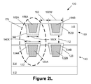
- FIG. 2L depicts the product 100 after one or more planarization processes, e.g., chemical mechanical polishing (CMP) processes, were performed to remove the excess portions of the conductive metal material 156 and the layer of conductive metal material 152 .
- CMP chemical mechanical polishing
- These process operations result in the definition of a plurality of upper inductor/transformer structures 160 , each of which is comprised of one of the metal core regions 156 A-B and one of the metal cap layers 152 A-B.
- the overall width 160 W and the lower surface area of each of the upper inductor/transformer structures 160 , as well as the lateral spacing 162 between the upper inductor/transformer structures 160 (when multiple structures 160 are present) may vary depending upon the application.
- the width 160 W (and the lower surface area of the upper inductor/transformer structures 160 ) and the lateral spacing 62 may generally correspond to the width 140 W (and the upper surface area of the lower inductor/transformer structures 140 ) and the lateral spacing 136 between the lower inductor/transformer structures 140 , although that need not be the case in each application.
- the lower surface area of the upper inductor/transformer structures 160 and the upper surface area of the lower inductor/transformer structures 140 may be different from one another, i.e., one surface area may be larger or smaller than the other surface area, or they both may be about the same, depending upon the particular application.
- a novel high performance inductor/transformer structure 170 may be comprised of one of the upper inductor/transformer structures 160 and one of the lower inductor/transformer structures 140 .
- the novel high performance inductor/transformer structure 170 may include both of the upper inductor/transformer structures 160 and both of the lower inductor/transformer structures 140 so as to enhance performance.
- the inductor/transformer structure 170 will exhibit many of the benefits and characteristics as that described above for the inductor/transformer structure 70 .
Landscapes
- Engineering & Computer Science (AREA)
- Power Engineering (AREA)
- Manufacturing & Machinery (AREA)
- Semiconductor Integrated Circuits (AREA)
- Coils Or Transformers For Communication (AREA)
Abstract
Description
Claims (22)
Priority Applications (1)
| Application Number | Priority Date | Filing Date | Title |
|---|---|---|---|
| US14/929,869 US9530553B1 (en) | 2015-11-02 | 2015-11-02 | High performance inductor/transformer and methods of making such inductor/transformer structures |
Applications Claiming Priority (1)
| Application Number | Priority Date | Filing Date | Title |
|---|---|---|---|
| US14/929,869 US9530553B1 (en) | 2015-11-02 | 2015-11-02 | High performance inductor/transformer and methods of making such inductor/transformer structures |
Publications (1)
| Publication Number | Publication Date |
|---|---|
| US9530553B1 true US9530553B1 (en) | 2016-12-27 |
Family
ID=57589972
Family Applications (1)
| Application Number | Title | Priority Date | Filing Date |
|---|---|---|---|
| US14/929,869 Expired - Fee Related US9530553B1 (en) | 2015-11-02 | 2015-11-02 | High performance inductor/transformer and methods of making such inductor/transformer structures |
Country Status (1)
| Country | Link |
|---|---|
| US (1) | US9530553B1 (en) |
Citations (4)
| Publication number | Priority date | Publication date | Assignee | Title |
|---|---|---|---|---|
| US20090309687A1 (en) * | 2008-06-11 | 2009-12-17 | Aleksandar Aleksov | Method of manufacturing an inductor for a microelectronic device, method of manufacturing a substrate containing such an inductor, and substrate manufactured thereby, |
| US20100254168A1 (en) * | 2009-03-31 | 2010-10-07 | Sriram Chandrasekaran | Magnetic Device Formed with U-Shaped Core Pieces and Power Converter Employing the Same |
| US20100259350A1 (en) * | 2009-04-14 | 2010-10-14 | Biar Jeff | Inductor or transformer for microelectric system |
| US9048021B2 (en) * | 2010-05-05 | 2015-06-02 | Nxp B.V. | Integrated transformer |
-
2015
- 2015-11-02 US US14/929,869 patent/US9530553B1/en not_active Expired - Fee Related
Patent Citations (4)
| Publication number | Priority date | Publication date | Assignee | Title |
|---|---|---|---|---|
| US20090309687A1 (en) * | 2008-06-11 | 2009-12-17 | Aleksandar Aleksov | Method of manufacturing an inductor for a microelectronic device, method of manufacturing a substrate containing such an inductor, and substrate manufactured thereby, |
| US20100254168A1 (en) * | 2009-03-31 | 2010-10-07 | Sriram Chandrasekaran | Magnetic Device Formed with U-Shaped Core Pieces and Power Converter Employing the Same |
| US20100259350A1 (en) * | 2009-04-14 | 2010-10-14 | Biar Jeff | Inductor or transformer for microelectric system |
| US9048021B2 (en) * | 2010-05-05 | 2015-06-02 | Nxp B.V. | Integrated transformer |
Similar Documents
| Publication | Publication Date | Title |
|---|---|---|
| US7381607B2 (en) | Method of forming a spiral inductor in a semiconductor substrate | |
| US6903644B2 (en) | Inductor device having improved quality factor | |
| US20090002115A1 (en) | Method to improve inductance with a high-permeability slotted plate core in an integrated circuit | |
| US7867787B2 (en) | Forming inductor and transformer structures with magnetic materials using damascene processing for integrated circuits | |
| JP4948756B2 (en) | Inductor formed in integrated circuit and method of manufacturing the same | |
| JP4904813B2 (en) | Semiconductor device and manufacturing method thereof | |
| US10276674B2 (en) | Method of forming a gate contact structure and source/drain contact structure for a semiconductor device | |
| US9362222B2 (en) | Interconnection between inductor and metal-insulator-metal (MIM) capacitor | |
| US20130147023A1 (en) | Integrated circuit ground shielding structure | |
| US9899321B1 (en) | Methods of forming a gate contact for a semiconductor device above the active region | |
| US10297452B2 (en) | Methods of forming a gate contact structure for a transistor | |
| CN106876423A (en) | It is integrated with the semiconductor structure and its manufacture method of MTJ | |
| US20190148240A1 (en) | Gate contact structures and cross-coupled contact structures for transistor devices | |
| US7633368B2 (en) | On-chip inductor | |
| US9613897B2 (en) | Integrated circuits including magnetic core inductors and methods for fabricating the same | |
| US8580647B2 (en) | Inductors with through VIAS | |
| US9219106B2 (en) | Integrated inductor | |
| US9530553B1 (en) | High performance inductor/transformer and methods of making such inductor/transformer structures | |
| US8859418B2 (en) | Methods of forming conductive structures using a dual metal hard mask technique | |
| US20100052095A1 (en) | Inductor for semiconductor device and method of fabricating the same | |
| CN110459535B (en) | Manufacturing method of laminated inductor and manufactured device | |
| US7754575B2 (en) | Inductor and method for manufacturing the same | |
| US11610839B2 (en) | Dummy fill structures | |
| US20160260794A1 (en) | Coil inductor | |
| KR20050062069A (en) | Method of manufacturing radio frequency semiconductor device |
Legal Events
| Date | Code | Title | Description |
|---|---|---|---|
| AS | Assignment |
Owner name: GLOBALFOUNDRIES INC., CAYMAN ISLANDS Free format text: ASSIGNMENT OF ASSIGNORS INTEREST;ASSIGNORS:SINGH, SUNIL;SINGH, JAGAR;MARRIA, PANKAJ;SIGNING DATES FROM 20151015 TO 20151028;REEL/FRAME:036936/0302 |
|
| STCF | Information on status: patent grant |
Free format text: PATENTED CASE |
|
| AS | Assignment |
Owner name: WILMINGTON TRUST, NATIONAL ASSOCIATION, DELAWARE Free format text: SECURITY AGREEMENT;ASSIGNOR:GLOBALFOUNDRIES INC.;REEL/FRAME:049490/0001 Effective date: 20181127 |
|
| FEPP | Fee payment procedure |
Free format text: MAINTENANCE FEE REMINDER MAILED (ORIGINAL EVENT CODE: REM.); ENTITY STATUS OF PATENT OWNER: LARGE ENTITY |
|
| AS | Assignment |
Owner name: GLOBALFOUNDRIES INC., CAYMAN ISLANDS Free format text: RELEASE BY SECURED PARTY;ASSIGNOR:WILMINGTON TRUST, NATIONAL ASSOCIATION;REEL/FRAME:054636/0001 Effective date: 20201117 |
|
| LAPS | Lapse for failure to pay maintenance fees |
Free format text: PATENT EXPIRED FOR FAILURE TO PAY MAINTENANCE FEES (ORIGINAL EVENT CODE: EXP.); ENTITY STATUS OF PATENT OWNER: LARGE ENTITY |
|
| STCH | Information on status: patent discontinuation |
Free format text: PATENT EXPIRED DUE TO NONPAYMENT OF MAINTENANCE FEES UNDER 37 CFR 1.362 |
|
| FP | Lapsed due to failure to pay maintenance fee |
Effective date: 20201227 |
|
| AS | Assignment |
Owner name: GLOBALFOUNDRIES U.S. INC., NEW YORK Free format text: RELEASE BY SECURED PARTY;ASSIGNOR:WILMINGTON TRUST, NATIONAL ASSOCIATION;REEL/FRAME:056987/0001 Effective date: 20201117 |