US9520344B2 - Semiconductor module for electric power - Google Patents
Semiconductor module for electric power Download PDFInfo
- Publication number
- US9520344B2 US9520344B2 US14/401,556 US201314401556A US9520344B2 US 9520344 B2 US9520344 B2 US 9520344B2 US 201314401556 A US201314401556 A US 201314401556A US 9520344 B2 US9520344 B2 US 9520344B2
- Authority
- US
- United States
- Prior art keywords
- frame
- island
- conductor
- electric
- metal
- Prior art date
- Legal status (The legal status is an assumption and is not a legal conclusion. Google has not performed a legal analysis and makes no representation as to the accuracy of the status listed.)
- Active, expires
Links
Images


Classifications
-
- H—ELECTRICITY
- H10—SEMICONDUCTOR DEVICES; ELECTRIC SOLID-STATE DEVICES NOT OTHERWISE PROVIDED FOR
- H10W—GENERIC PACKAGES, INTERCONNECTIONS, CONNECTORS OR OTHER CONSTRUCTIONAL DETAILS OF DEVICES COVERED BY CLASS H10
- H10W70/00—Package substrates; Interposers; Redistribution layers [RDL]
- H10W70/40—Leadframes
- H10W70/421—Shapes or dispositions
- H10W70/424—Cross-sectional shapes
-
- H01L23/49548—
-
- H01L23/043—
-
- H01L23/34—
-
- H01L23/49517—
-
- H01L23/49534—
-
- H01L23/49537—
-
- H01L23/49541—
-
- H01L23/49575—
-
- H01L25/07—
-
- H01L25/18—
-
- H01L27/0629—
-
- H—ELECTRICITY
- H10—SEMICONDUCTOR DEVICES; ELECTRIC SOLID-STATE DEVICES NOT OTHERWISE PROVIDED FOR
- H10D—INORGANIC ELECTRIC SEMICONDUCTOR DEVICES
- H10D84/00—Integrated devices formed in or on semiconductor substrates that comprise only semiconducting layers, e.g. on Si wafers or on GaAs-on-Si wafers
- H10D84/80—Integrated devices formed in or on semiconductor substrates that comprise only semiconducting layers, e.g. on Si wafers or on GaAs-on-Si wafers characterised by the integration of at least one component covered by groups H10D12/00 or H10D30/00, e.g. integration of IGFETs
- H10D84/811—Combinations of field-effect devices and one or more diodes, capacitors or resistors
-
- H—ELECTRICITY
- H10—SEMICONDUCTOR DEVICES; ELECTRIC SOLID-STATE DEVICES NOT OTHERWISE PROVIDED FOR
- H10W—GENERIC PACKAGES, INTERCONNECTIONS, CONNECTORS OR OTHER CONSTRUCTIONAL DETAILS OF DEVICES COVERED BY CLASS H10
- H10W40/00—Arrangements for thermal protection or thermal control
-
- H—ELECTRICITY
- H10—SEMICONDUCTOR DEVICES; ELECTRIC SOLID-STATE DEVICES NOT OTHERWISE PROVIDED FOR
- H10W—GENERIC PACKAGES, INTERCONNECTIONS, CONNECTORS OR OTHER CONSTRUCTIONAL DETAILS OF DEVICES COVERED BY CLASS H10
- H10W70/00—Package substrates; Interposers; Redistribution layers [RDL]
- H10W70/40—Leadframes
- H10W70/421—Shapes or dispositions
- H10W70/442—Shapes or dispositions of multiple leadframes in a single chip
-
- H—ELECTRICITY
- H10—SEMICONDUCTOR DEVICES; ELECTRIC SOLID-STATE DEVICES NOT OTHERWISE PROVIDED FOR
- H10W—GENERIC PACKAGES, INTERCONNECTIONS, CONNECTORS OR OTHER CONSTRUCTIONAL DETAILS OF DEVICES COVERED BY CLASS H10
- H10W70/00—Package substrates; Interposers; Redistribution layers [RDL]
- H10W70/40—Leadframes
- H10W70/451—Multilayered leadframes
-
- H—ELECTRICITY
- H10—SEMICONDUCTOR DEVICES; ELECTRIC SOLID-STATE DEVICES NOT OTHERWISE PROVIDED FOR
- H10W—GENERIC PACKAGES, INTERCONNECTIONS, CONNECTORS OR OTHER CONSTRUCTIONAL DETAILS OF DEVICES COVERED BY CLASS H10
- H10W70/00—Package substrates; Interposers; Redistribution layers [RDL]
- H10W70/40—Leadframes
- H10W70/464—Additional interconnections in combination with leadframes
-
- H—ELECTRICITY
- H10—SEMICONDUCTOR DEVICES; ELECTRIC SOLID-STATE DEVICES NOT OTHERWISE PROVIDED FOR
- H10W—GENERIC PACKAGES, INTERCONNECTIONS, CONNECTORS OR OTHER CONSTRUCTIONAL DETAILS OF DEVICES COVERED BY CLASS H10
- H10W76/00—Containers; Fillings or auxiliary members therefor; Seals
- H10W76/10—Containers or parts thereof
- H10W76/12—Containers or parts thereof characterised by their shape
- H10W76/13—Containers comprising a conductive base serving as an interconnection
-
- H—ELECTRICITY
- H10—SEMICONDUCTOR DEVICES; ELECTRIC SOLID-STATE DEVICES NOT OTHERWISE PROVIDED FOR
- H10W—GENERIC PACKAGES, INTERCONNECTIONS, CONNECTORS OR OTHER CONSTRUCTIONAL DETAILS OF DEVICES COVERED BY CLASS H10
- H10W90/00—Package configurations
-
- H—ELECTRICITY
- H10—SEMICONDUCTOR DEVICES; ELECTRIC SOLID-STATE DEVICES NOT OTHERWISE PROVIDED FOR
- H10W—GENERIC PACKAGES, INTERCONNECTIONS, CONNECTORS OR OTHER CONSTRUCTIONAL DETAILS OF DEVICES COVERED BY CLASS H10
- H10W90/00—Package configurations
- H10W90/811—Multiple chips on leadframes
-
- H01L2224/32245—
-
- H01L2224/37124—
-
- H01L2224/37147—
-
- H01L2224/40247—
-
- H01L2224/45014—
-
- H01L2224/45124—
-
- H01L2224/45147—
-
- H01L2224/48247—
-
- H01L2224/4903—
-
- H01L2224/73221—
-
- H01L2224/73263—
-
- H01L2224/73265—
-
- H01L23/24—
-
- H01L23/28—
-
- H01L23/3735—
-
- H01L23/4334—
-
- H01L23/49589—
-
- H01L23/49811—
-
- H01L24/32—
-
- H01L24/37—
-
- H01L24/40—
-
- H01L24/45—
-
- H01L24/48—
-
- H01L24/49—
-
- H01L24/73—
-
- H01L2924/00—
-
- H01L2924/00012—
-
- H01L2924/01015—
-
- H01L2924/1305—
-
- H01L2924/13055—
-
- H01L2924/13091—
-
- H01L2924/30107—
-
- H—ELECTRICITY
- H10—SEMICONDUCTOR DEVICES; ELECTRIC SOLID-STATE DEVICES NOT OTHERWISE PROVIDED FOR
- H10W—GENERIC PACKAGES, INTERCONNECTIONS, CONNECTORS OR OTHER CONSTRUCTIONAL DETAILS OF DEVICES COVERED BY CLASS H10
- H10W40/00—Arrangements for thermal protection or thermal control
- H10W40/20—Arrangements for cooling
- H10W40/25—Arrangements for cooling characterised by their materials
- H10W40/255—Arrangements for cooling characterised by their materials having a laminate or multilayered structure, e.g. direct bond copper [DBC] ceramic substrates
-
- H—ELECTRICITY
- H10—SEMICONDUCTOR DEVICES; ELECTRIC SOLID-STATE DEVICES NOT OTHERWISE PROVIDED FOR
- H10W—GENERIC PACKAGES, INTERCONNECTIONS, CONNECTORS OR OTHER CONSTRUCTIONAL DETAILS OF DEVICES COVERED BY CLASS H10
- H10W40/00—Arrangements for thermal protection or thermal control
- H10W40/70—Fillings or auxiliary members in containers or in encapsulations for thermal protection or control
- H10W40/77—Auxiliary members characterised by their shape
- H10W40/778—Auxiliary members characterised by their shape in encapsulations
-
- H—ELECTRICITY
- H10—SEMICONDUCTOR DEVICES; ELECTRIC SOLID-STATE DEVICES NOT OTHERWISE PROVIDED FOR
- H10W—GENERIC PACKAGES, INTERCONNECTIONS, CONNECTORS OR OTHER CONSTRUCTIONAL DETAILS OF DEVICES COVERED BY CLASS H10
- H10W70/00—Package substrates; Interposers; Redistribution layers [RDL]
- H10W70/40—Leadframes
- H10W70/475—Capacitors in combination with leadframes
-
- H—ELECTRICITY
- H10—SEMICONDUCTOR DEVICES; ELECTRIC SOLID-STATE DEVICES NOT OTHERWISE PROVIDED FOR
- H10W—GENERIC PACKAGES, INTERCONNECTIONS, CONNECTORS OR OTHER CONSTRUCTIONAL DETAILS OF DEVICES COVERED BY CLASS H10
- H10W72/00—Interconnections or connectors in packages
- H10W72/071—Connecting or disconnecting
- H10W72/075—Connecting or disconnecting of bond wires
- H10W72/07502—Connecting or disconnecting of bond wires using an auxiliary member
- H10W72/07504—Connecting or disconnecting of bond wires using an auxiliary member the auxiliary member being temporary, e.g. a sacrificial coating
-
- H—ELECTRICITY
- H10—SEMICONDUCTOR DEVICES; ELECTRIC SOLID-STATE DEVICES NOT OTHERWISE PROVIDED FOR
- H10W—GENERIC PACKAGES, INTERCONNECTIONS, CONNECTORS OR OTHER CONSTRUCTIONAL DETAILS OF DEVICES COVERED BY CLASS H10
- H10W72/00—Interconnections or connectors in packages
- H10W72/071—Connecting or disconnecting
- H10W72/075—Connecting or disconnecting of bond wires
- H10W72/07551—Connecting or disconnecting of bond wires characterised by changes in properties of the bond wires during the connecting
- H10W72/07552—Connecting or disconnecting of bond wires characterised by changes in properties of the bond wires during the connecting changes in structures or sizes
-
- H—ELECTRICITY
- H10—SEMICONDUCTOR DEVICES; ELECTRIC SOLID-STATE DEVICES NOT OTHERWISE PROVIDED FOR
- H10W—GENERIC PACKAGES, INTERCONNECTIONS, CONNECTORS OR OTHER CONSTRUCTIONAL DETAILS OF DEVICES COVERED BY CLASS H10
- H10W72/00—Interconnections or connectors in packages
- H10W72/50—Bond wires
- H10W72/521—Structures or relative sizes of bond wires
- H10W72/527—Multiple bond wires having different sizes
-
- H—ELECTRICITY
- H10—SEMICONDUCTOR DEVICES; ELECTRIC SOLID-STATE DEVICES NOT OTHERWISE PROVIDED FOR
- H10W—GENERIC PACKAGES, INTERCONNECTIONS, CONNECTORS OR OTHER CONSTRUCTIONAL DETAILS OF DEVICES COVERED BY CLASS H10
- H10W72/00—Interconnections or connectors in packages
- H10W72/50—Bond wires
- H10W72/531—Shapes of wire connectors
- H10W72/533—Cross-sectional shape
- H10W72/534—Cross-sectional shape being rectangular
-
- H—ELECTRICITY
- H10—SEMICONDUCTOR DEVICES; ELECTRIC SOLID-STATE DEVICES NOT OTHERWISE PROVIDED FOR
- H10W—GENERIC PACKAGES, INTERCONNECTIONS, CONNECTORS OR OTHER CONSTRUCTIONAL DETAILS OF DEVICES COVERED BY CLASS H10
- H10W72/00—Interconnections or connectors in packages
- H10W72/50—Bond wires
- H10W72/531—Shapes of wire connectors
- H10W72/536—Shapes of wire connectors the connected ends being ball-shaped
-
- H—ELECTRICITY
- H10—SEMICONDUCTOR DEVICES; ELECTRIC SOLID-STATE DEVICES NOT OTHERWISE PROVIDED FOR
- H10W—GENERIC PACKAGES, INTERCONNECTIONS, CONNECTORS OR OTHER CONSTRUCTIONAL DETAILS OF DEVICES COVERED BY CLASS H10
- H10W72/00—Interconnections or connectors in packages
- H10W72/50—Bond wires
- H10W72/531—Shapes of wire connectors
- H10W72/5363—Shapes of wire connectors the connected ends being wedge-shaped
-
- H—ELECTRICITY
- H10—SEMICONDUCTOR DEVICES; ELECTRIC SOLID-STATE DEVICES NOT OTHERWISE PROVIDED FOR
- H10W—GENERIC PACKAGES, INTERCONNECTIONS, CONNECTORS OR OTHER CONSTRUCTIONAL DETAILS OF DEVICES COVERED BY CLASS H10
- H10W72/00—Interconnections or connectors in packages
- H10W72/50—Bond wires
- H10W72/551—Materials of bond wires
- H10W72/552—Materials of bond wires comprising metals or metalloids, e.g. silver
- H10W72/5524—Materials of bond wires comprising metals or metalloids, e.g. silver comprising aluminium [Al]
-
- H—ELECTRICITY
- H10—SEMICONDUCTOR DEVICES; ELECTRIC SOLID-STATE DEVICES NOT OTHERWISE PROVIDED FOR
- H10W—GENERIC PACKAGES, INTERCONNECTIONS, CONNECTORS OR OTHER CONSTRUCTIONAL DETAILS OF DEVICES COVERED BY CLASS H10
- H10W72/00—Interconnections or connectors in packages
- H10W72/50—Bond wires
- H10W72/551—Materials of bond wires
- H10W72/552—Materials of bond wires comprising metals or metalloids, e.g. silver
- H10W72/5525—Materials of bond wires comprising metals or metalloids, e.g. silver comprising copper [Cu]
-
- H—ELECTRICITY
- H10—SEMICONDUCTOR DEVICES; ELECTRIC SOLID-STATE DEVICES NOT OTHERWISE PROVIDED FOR
- H10W—GENERIC PACKAGES, INTERCONNECTIONS, CONNECTORS OR OTHER CONSTRUCTIONAL DETAILS OF DEVICES COVERED BY CLASS H10
- H10W72/00—Interconnections or connectors in packages
- H10W72/60—Strap connectors, e.g. thick copper clips for grounding of power devices
- H10W72/651—Materials of strap connectors
- H10W72/652—Materials of strap connectors comprising metals or metalloids, e.g. silver
-
- H—ELECTRICITY
- H10—SEMICONDUCTOR DEVICES; ELECTRIC SOLID-STATE DEVICES NOT OTHERWISE PROVIDED FOR
- H10W—GENERIC PACKAGES, INTERCONNECTIONS, CONNECTORS OR OTHER CONSTRUCTIONAL DETAILS OF DEVICES COVERED BY CLASS H10
- H10W72/00—Interconnections or connectors in packages
- H10W72/851—Dispositions of multiple connectors or interconnections
- H10W72/853—On the same surface
- H10W72/871—Bond wires and strap connectors
-
- H—ELECTRICITY
- H10—SEMICONDUCTOR DEVICES; ELECTRIC SOLID-STATE DEVICES NOT OTHERWISE PROVIDED FOR
- H10W—GENERIC PACKAGES, INTERCONNECTIONS, CONNECTORS OR OTHER CONSTRUCTIONAL DETAILS OF DEVICES COVERED BY CLASS H10
- H10W72/00—Interconnections or connectors in packages
- H10W72/851—Dispositions of multiple connectors or interconnections
- H10W72/874—On different surfaces
- H10W72/884—Die-attach connectors and bond wires
-
- H—ELECTRICITY
- H10—SEMICONDUCTOR DEVICES; ELECTRIC SOLID-STATE DEVICES NOT OTHERWISE PROVIDED FOR
- H10W—GENERIC PACKAGES, INTERCONNECTIONS, CONNECTORS OR OTHER CONSTRUCTIONAL DETAILS OF DEVICES COVERED BY CLASS H10
- H10W72/00—Interconnections or connectors in packages
- H10W72/851—Dispositions of multiple connectors or interconnections
- H10W72/874—On different surfaces
- H10W72/886—Die-attach connectors and strap connectors
-
- H—ELECTRICITY
- H10—SEMICONDUCTOR DEVICES; ELECTRIC SOLID-STATE DEVICES NOT OTHERWISE PROVIDED FOR
- H10W—GENERIC PACKAGES, INTERCONNECTIONS, CONNECTORS OR OTHER CONSTRUCTIONAL DETAILS OF DEVICES COVERED BY CLASS H10
- H10W74/00—Encapsulations, e.g. protective coatings
-
- H—ELECTRICITY
- H10—SEMICONDUCTOR DEVICES; ELECTRIC SOLID-STATE DEVICES NOT OTHERWISE PROVIDED FOR
- H10W—GENERIC PACKAGES, INTERCONNECTIONS, CONNECTORS OR OTHER CONSTRUCTIONAL DETAILS OF DEVICES COVERED BY CLASS H10
- H10W76/00—Containers; Fillings or auxiliary members therefor; Seals
- H10W76/40—Fillings or auxiliary members in containers, e.g. centering rings
- H10W76/42—Fillings
- H10W76/47—Solid or gel fillings
-
- H—ELECTRICITY
- H10—SEMICONDUCTOR DEVICES; ELECTRIC SOLID-STATE DEVICES NOT OTHERWISE PROVIDED FOR
- H10W—GENERIC PACKAGES, INTERCONNECTIONS, CONNECTORS OR OTHER CONSTRUCTIONAL DETAILS OF DEVICES COVERED BY CLASS H10
- H10W90/00—Package configurations
- H10W90/701—Package configurations characterised by the relative positions of pads or connectors relative to package parts
- H10W90/731—Package configurations characterised by the relative positions of pads or connectors relative to package parts of die-attach connectors
- H10W90/736—Package configurations characterised by the relative positions of pads or connectors relative to package parts of die-attach connectors between a chip and a stacked lead frame, conducting package substrate or heat sink
-
- H—ELECTRICITY
- H10—SEMICONDUCTOR DEVICES; ELECTRIC SOLID-STATE DEVICES NOT OTHERWISE PROVIDED FOR
- H10W—GENERIC PACKAGES, INTERCONNECTIONS, CONNECTORS OR OTHER CONSTRUCTIONAL DETAILS OF DEVICES COVERED BY CLASS H10
- H10W90/00—Package configurations
- H10W90/701—Package configurations characterised by the relative positions of pads or connectors relative to package parts
- H10W90/751—Package configurations characterised by the relative positions of pads or connectors relative to package parts of bond wires
- H10W90/752—Package configurations characterised by the relative positions of pads or connectors relative to package parts of bond wires between stacked chips
-
- H—ELECTRICITY
- H10—SEMICONDUCTOR DEVICES; ELECTRIC SOLID-STATE DEVICES NOT OTHERWISE PROVIDED FOR
- H10W—GENERIC PACKAGES, INTERCONNECTIONS, CONNECTORS OR OTHER CONSTRUCTIONAL DETAILS OF DEVICES COVERED BY CLASS H10
- H10W90/00—Package configurations
- H10W90/701—Package configurations characterised by the relative positions of pads or connectors relative to package parts
- H10W90/751—Package configurations characterised by the relative positions of pads or connectors relative to package parts of bond wires
- H10W90/756—Package configurations characterised by the relative positions of pads or connectors relative to package parts of bond wires between a chip and a stacked lead frame, conducting package substrate or heat sink
-
- H—ELECTRICITY
- H10—SEMICONDUCTOR DEVICES; ELECTRIC SOLID-STATE DEVICES NOT OTHERWISE PROVIDED FOR
- H10W—GENERIC PACKAGES, INTERCONNECTIONS, CONNECTORS OR OTHER CONSTRUCTIONAL DETAILS OF DEVICES COVERED BY CLASS H10
- H10W90/00—Package configurations
- H10W90/701—Package configurations characterised by the relative positions of pads or connectors relative to package parts
- H10W90/761—Package configurations characterised by the relative positions of pads or connectors relative to package parts of strap connectors
- H10W90/766—Package configurations characterised by the relative positions of pads or connectors relative to package parts of strap connectors between a chip and a stacked lead frame, conducting package substrate or heat sink
Definitions
- An aspect of the present invention is what relates to structure of a semiconductor module for electric power.
- an insulating gate-type bipolar transistor IGBT
- a transistor using a wide-band-gap-system semiconductor element (SiC or GaN) for electric power.
- an insulating gate-type transistor using silicon carbide (SiC) which is of high voltage-resistance and able to realize low-temperature resistance, is capable of carrying out high-speed operation for the reason of its being a unipolar-type device, and practical use is expected.
- the heat generation from the semiconductor element occupies most of it. What is by the conduction loss of heat generation carried out when electric current flows in the device, and what is by the switching loss which is generated at the time of switching on the occasion of transit of the device from an ON state to an OFF state or from an OFF state to an ON state occupy most portions of the heat generation from the semiconductor element.
- FIG. 10 a plan view of a conventional semiconductor module for electric power is shown, according to Japanese Patent Application Publication No. 2004-22960.
- this semiconductor module for electric power adopted is an arrangement such that chips are lined in parallel inside the arm in order to carry out electric current enlarging, the busbars are arranged at the center, and the configuration is allowed to be such that the high-side side element group 73 and the low-side side element group 74 sandwich the busbars.
- the present invention furnishes, in consideration of the above-mentioned conventional problems, a semiconductor module for electric power which miniaturizes the module size and is able to reduce the wiring inductance.
- the 1 st aspect of the present invention is
- a semiconductor module for electric power comprising:
- a third frame which is electrically connected to the first intermediate frame, and is arranged above the first frame;
- a fourth frame which is electrically connected to the second intermediate frame, and is arranged above the second frame;
- a drain electrode of the first transistor is connected to the first frame
- a source electrode of the first transistor and an anode electrode of the first diode are connected to the first intermediate frame with first connecting lines of metal
- a drain electrode of the second transistor is connected to the second frame
- a source electrode of the second transistor and an anode electrode of the second diode are connected to the second intermediate frame with second connecting lines of metal,
- gate terminals and source terminals are arranged,
- all the frames are arranged on a heat radiating plate via an insulator which is configured with a resin-system material, and at least a part of all the frames is covered with a molding resin, and
- the third frame and the fourth frame are arranged in parallel with each other, and the electric source terminal, the ground terminal and the output terminal are arranged in a manner such that induced electric voltages, which are generated in the third frame and the fourth frame, become in reverse directions with each other.
- the foot of the third frame is arranged between the plural first connecting lines, and
- the foot of the fourth frame is arranged between the plural second connecting lines.
- the third frame is arranged so as to be placed above the first transistors and the first diodes, and
- the fourth frame is arranged so as to be placed above the second transistors and the second diodes.
- a gate electrode of the first transistor is arranged at a side opposite to the first intermediate frame
- a gate electrode of the second transistor is arranged at a side opposite to the second intermediate frame.
- a semiconductor module for electric power comprising:
- a fifth frame which is electrically connected to the first intermediate metal electric-conductor-island, and is arranged above the first metal electric-conductor-island;
- a sixth frame which is electrically connected to the second intermediate metal electric-conductor-island, and is arranged above the second metal electric-conductor-island;
- a drain electrode of the first transistor is connected to the first metal electric-conductor-island
- a source electrode of the first transistor and an anode electrode of the first diode are connected to the first intermediate metal electric-conductor-island with first connecting lines of metal,
- a drain electrode of the second transistor is connected to the second metal electric-conductor-island
- a source electrode of the second transistor and an anode electrode of the second diode are connected to the second intermediate metal electric-conductor-island with second connecting lines of metal,
- gate terminals and source terminals are arranged,
- all the metal electric-conductor-islands are arranged on a heat radiating plate via an insulator which is configured with a ceramic material, and at least a part of all the metal electric-conductor-islands is covered with a gel-like resin, and
- the fifth frame and the sixth frame are arranged in parallel with each other, and the electric source terminal, the ground terminal and the output terminal are arranged in a manner such that induced electric voltages, which are generated in the fifth frame and the sixth frame, become in reverse directions with each other.
- the foot of the fifth frame is arranged between the plural first connecting lines, and
- the foot of the sixth frame is arranged between the plural second connecting lines.
- the fifth frame is arranged so as to be placed above the first transistors and the first diodes, and
- the sixth frame is arranged so as to be placed above the second transistors and the second diodes.
- the first connecting lines and the second connecting lines are configured with ribbons.
- the first connecting lines and the second connecting lines are configured with clips.
- a gate electrode of the first transistor is arranged at a side opposite to the first intermediate metal electric-conductor-island, and
- a gate electrode of the second transistor is arranged at a side opposite to the second intermediate metal electric-conductor-island.
- the 11 th aspect of the present invention is
- the first connecting lines and the second connecting lines are configured with ribbons.
- the 12 th aspect of the present invention is
- the first connecting lines and the second connecting lines are configured with clips.
- a semiconductor module for electric power is able to be furnished which miniaturizes the module size and is able to reduce the wiring inductance.
- FIG. 1( a ) is a plan view of the semiconductor module for electric power in Embodiment 1 of the present invention
- FIG. 1( b ) is a section view of the semiconductor module for electric power in Embodiment 1 of the present invention, in A-A′ of FIG. 1( a )
- FIG. 1( c ) is a section view of a modified example of the semiconductor module for electric power in Embodiment 1 of the present invention.
- FIGS. 2( a )-( f ) are plan views which show the assembly flow of the semiconductor module for electric power of Embodiment 1 of the present invention.
- FIG. 3( a ) is a plan view of the semiconductor module for electric power in Embodiment 2 of the present invention
- FIG. 3( b ) is a section view of the semiconductor module for electric power in Embodiment 2 of the present invention, in B-B′ of FIG. 3( a )
- FIG. 3( c ) is a section view of a modified example of the semiconductor module for electric power in Embodiment 2 of the present invention.
- FIGS. 4( a )-( f ) are plan views which show the assembly flow of the semiconductor module for electric power of Embodiment 2 of the present invention.
- FIG. 5( a ) is a plan view of the semiconductor module for electric power in Embodiment 3 of the present invention
- FIG. 5( b ) is a section view of the semiconductor module for electric power in Embodiment 3 of the present invention, in A-A′ of FIG. 5( a ) .
- FIGS. 6( a )-( e ) are plan views which show the assembly flow of the semiconductor module for electric power of Embodiment 3 of the present invention.
- FIG. 7 is an equivalency circuit diagram of the semiconductor module for electric power in Embodiment 3 of the present invention.
- FIG. 8( a ) is a plan view of the semiconductor module for electric power in Embodiment 4 of the present invention
- FIG. 8( b ) is a section view of the semiconductor module for electric power in Embodiment 4 of the present invention, in B-B′ of FIG. 8( a ) .
- FIGS. 9( a )-( e ) are plan views which show the assembly flow of the semiconductor module for electric power of Embodiment 4 of the present invention.
- FIG. 10 is a plan view of the conventional semiconductor module for electric power.
- FIG. 1( a ) Shown in FIG. 1( a ) is the module configuration 101 which is a plan view of the semiconductor module for electric power of a resin-sealing-type of Embodiment 1 of the present invention.
- FIG. 1( b ) shown in FIG. 1( b ) is the section configuration 102 of the semiconductor module for electric power of the present Embodiment 1 such that cutting is carried out with A-A′ in FIG. 1( a ) .
- FIG. 2( a ) - FIG. 2( f ) an assembly flow diagram of the semiconductor module for electric power of the present Embodiment 1 is shown.
- FIG. 2( a ) - FIG. 2( f ) show, respectively, plan views at the time of assembly of the semiconductor module for electric power of the present Embodiment 1.
- FIG. 2( a ) is a plan view of the first frame 1 , the second frame 2 , the first intermediate frame 5 , the second intermediate frame 6 , the high-side side gate terminals 7 , the low-side side source terminals 20 , the high-side side source terminals 8 , and the low-side side gate terminals 21 , which are the lead frames of groundwork.
- these leads are fixed to a rim so as not to come apart, and are cut off from the rim after the final molding is completed, but there are omissions in regards to detailed descriptions of this portion.
- the transistor chips 11 and the diode chips 12 are semiconductor elements.
- the transistor chip 11 a transistor like an IGBT or an SiC-MOSFET is mounted.
- the drain electrode or the collector electrode of the transistor chip 11 is mounted on the first frame 1 and the second frame 2
- the cathode electrode of the diode chip 12 is mounted on the first frame 1 and the second frame 2 .
- the semiconductor module for electric power of the present Embodiment 1 shown is an example such that, on one arm, three transistor chips 11 like an IGBT or an SiC-MOSFET and three diode chips 12 are alternately arranged.
- the source electrode or the emitter electrode of the transistor chip 11 which has been mounted on the first frame 1 is wire-connected to the first intermediate frame 5
- the source electrode or the emitter electrode of the transistor chip 11 which has been mounted on the second frame 2 is wire-connected to the second intermediate frame 6 .
- the gate pad 13 of the transistor chip 11 which has been mounted on the first frame 1 and the gate terminal 7 on the high-side side of the lead frame are wire-connected, and the source pad of the transistor chip 11 and the source terminal 8 on the high-side side of the lead frame are wire-connected.
- the gate pad 13 of the transistor chip 11 which has been mounted on the second frame 2 and the gate terminal 21 on the low-side side of the lead frame are wire-connected, and the source pad of the transistor chip 11 and the source terminal 20 on the low-side side of the lead frame are wire-connected.
- FIG. 2( c ) prepared are the third frame 3 on the positive electrode side which functions as a busbar, and the fourth frame 4 on the negative electrode side.
- the fourth frame 4 is arranged above the second frame 2 , and the feet of the fourth frame 4 are metal-bonded to the second intermediate frame 6 .
- the third frame 3 is arranged above the first frame 1 , and the third frame 3 is metal-bonded at the bonding point 50 , to the second frame 2 . Moreover, the feet of the third frame 3 are metal-bonded to the first intermediate frame 5 .
- FIG. 2( f ) molding is carried out by the insulating resin 18 , the whole is sealed with the shape which is regulated with the outer rim 19 of the insulating resin, and thereby fixation of the module is carried out.
- the semiconductor module for electric power of the present Embodiment 1 is thereby finished.
- FIG. 1( a ) and FIG. 1( b ) descriptions are given regarding the configuration of the semiconductor module for electric power of the present Embodiment 1 which is manufactured through the assembly flow shown in FIG. 2( a ) - FIG. 2( f ) .
- Gluing by a die-bond material is carried out, and thereby onto the first frame 1 and onto the second frame 2 plural semiconductor chips are mounted. These semiconductor chips are configured with the transistor chips 11 and the diode chips 12 .
- the first frame 1 and the second frame 2 are arranged on the heat radiating plate 17 via the insulator 16 . It is good that the heat radiating plate 17 is configured with a material like Cu or Al such that the heat conduction rate is large. It is good that the insulator 16 is configured with a material such that the heat conduction property is good, and the electric insulation property is good as well.
- molding is carried out by the insulating resin 18 , and by the outer rim 19 of the insulating resin the shape of the module is defined.
- the configuration of the semiconductor module for electric power of the present Embodiment 1 which uses an SiC-MOSFET as the transistor chip 11 corresponds to an example of the semiconductor module for electric power of the present invention.
- the transistor chips 11 and the diode chips 12 mounted onto the first frame 1 correspond, respectively, to examples of the first transistors and the first diodes of the present invention.
- the transistor chips 11 and the diode chips 12 mounted onto the second frame 2 correspond, respectively, to examples of the second transistors and the second diodes of the present invention.
- first intermediate frame 5 and the second intermediate frame 6 which are narrow in width compared with these frames are arranged, with the first intermediate frame 5 at the side near to the first frame 1 roughly in parallel, and the second intermediate frame 6 at the side near to the second frame 2 roughly in parallel.
- the first intermediate frame 5 and the second intermediate frame 6 are, with reference to the center line of the semiconductor module for electric power, namely the line which in the plan view of FIG. 1( a ) , up and down bisects the module configuration 101 , arranged at the positions which sandwich that center line and face each other.
- connection is carried out from the source electrode or the emitter electrode of the transistor chip 11 on the first frame 1 to the first intermediate frame 5 with the connecting line 9 of metal, and connection is carried out from the anode electrode of the diode chip 12 on the first frame 1 to the first intermediate frame 5 with the connecting line 10 of metal.
- the feet of the third frame 3 which is arranged above the first frame 1 are connected.
- connection is carried out from the source electrode or the emitter electrode of the transistor chip 11 on the second frame 2 to the second intermediate frame 6 with the connecting line 9 of metal, and connection is carried out from the anode electrode of the diode chip 12 on the second frame 2 to the second intermediate frame 6 with the connecting line 10 of metal.
- the feet of the fourth frame 4 which is arranged above the second frame 2 are connected.
- connecting lines 9 and 10 of metal which connect the transistor chip 11 and the diode chip 12 on the first frame 1 , and the first intermediate frame 5 correspond to examples of the first connecting lines of metal of the present invention.
- the connecting lines 9 and 10 of metal which connect the transistor chip 11 and the diode chip 12 on the second frame 2 , and the second intermediate frame 6 correspond to examples of the second connecting lines of metal of the present invention.
- the configuration is allowed to be such that the third frame 3 is placed at least above the semiconductor-chip-installation-region of the first frame 1 , namely the region where the three transistor chips 11 and the three diode chips 12 are mounted. And similarly, it is desirable that the configuration is allowed to be such that the fourth frame 4 is placed at least above the semiconductor-chip-installation-region of the second frame 2 .
- the connecting line 9 of metal which is used to carry out connection from the source electrode or the emitter electrode of the transistor chip 11 on the first frame 1 to the first intermediate frame 5 is, usually, configured with a plurality of wires of Al, and also tolerates a large electric current.
- the configuration is allowed to be with a ribbon of Al or a ribbon of Cu, bonding reliability is thereby improved, and besides further electric current enlarging, high heat radiating property are able to be realized. Moreover, a similar function is capable of being realized even if an Al clip, a Cu clip or a clip composed of other materials is used, in lieu of the connecting line 9 of metal.
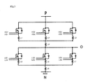
- the electric source terminal part 22 on an extension of the first frame 1 has a function as an electrode, and functions as a P (electric source) terminal.
- the ground terminal part 23 on an extension of the fourth frame 4 has a function as an electrode, and functions as an N (ground) terminal.
- line-tying is carried out at the metal bonding point 50 which is arranged at the side reverse to the P terminal and the N terminal, and the output terminal part 24 on an extension of the third frame 3 has a function as an electrode, and functions as an O (output) terminal.
- the third frame 3 and the fourth frame 4 are arranged in parallel with each other, the O terminal is in addition arranged at the side reverse to the P terminal and the N terminal, respective electric currents of the third frame 3 which is the positive-electrode side busbar and the fourth frame 4 which is the negative-electrode side busbar thereby flow in reverse directions and, with an effect of mutual inductance, the inductance is able to be allowed to reduce.
- the electric source terminal part 22 (the P terminal), the ground terminal part 23 (the N terminal) and the output terminal part 24 (the O terminal) are arranged.
- the first intermediate frame 5 , the second intermediate frame 6 , the third frame 3 and the fourth frame 4 are used in combination, since the space over the semiconductor chips is able to be utilized as wirings (busbars) of wide width which is able to realize inductance lowering, miniaturization of the semiconductor module for electric power is thereby also able to be realized and, because the arrangements of the first frame 1 and the second frame 2 which are installing the semiconductor chips are able to be allowed to come close, realization of further inductance lowering becomes capable of being achieved.
- the distance from the gate driver is configured to be shortest. Therefore, it is good that in neighborhoods of the respective transistors, the high-side side gate terminals 7 and the low-side side gate terminals 21 as leads which are for gate wirings, and the high-side side source terminals 8 and the low-side side source terminals 20 as leads which are for source wirings have been formed.
- Desirable is a configuration such that gate drivers are arranged to the respective transistor chips 11 but, particularly, in a use such that high-speed operation is not necessary, the configuration may be such that the gates of plural transistor chips or the sources are gathered to one lead.
- the gate wirings 14 of metal are formed from the gate pads 13 of the transistor chips 11 .
- the source wirings 15 of metal are formed.
- the configuration is allowed to be such that the gate electrode of the transistor chip 11 on the first frame 1 is, as shown in FIG. 1( a ) , arranged at the opposite side with the first intermediate frame 5 at the center of the semiconductor module for electric power, and the configuration is allowed to be such that the gate electrode of the transistor chip 11 on the second frame 2 is arranged at the opposite side with the second intermediate frame 6 at the center of the semiconductor module for electric power, which then leads to the wirings becoming short and is advantageous.
- the insulator 16 is arranged on the heat radiating plate 17 which is arranged at the lower face side, with each frame arranged thereon, and that the molding is carried out by the insulating resin 18 so as to be regulated with the outer rim 19 of the insulating resin.
- the number and arrangement of semiconductor chips are, since being determined in arbitrary combination with the electric current rating of the semiconductor module for electric power, not particularly regulated.
- Embodiment 1 the present invention has been described with a module of a resin-sealing-type, but the concept of the present invention is not limited to this and, even if applied to a module formed on a metal insulating substrate, similar effects are obtained. Even with other embodiments, similar effects are obtained.
- the module configuration 103 which is a plan view of the semiconductor module for electric power of a metal-insulating-substrate-type is shown in FIG. 3( a ) .
- FIG. 3( b ) shown in FIG. 3( b ) is the section configuration 104 of the semiconductor module for electric power of the present Embodiment 2 such that cutting is carried out with B-B′ in FIG. 3( a ) .
- FIG. 4( a ) - FIG. 4( f ) an assembly flow diagram of the semiconductor module for electric power of the present Embodiment 2 is shown.
- FIG. 4( a ) - FIG. 4( f ) show, respectively, plan views at the time of assembly of the semiconductor module for electric power of the present Embodiment 2.
- FIG. 4( a ) is a wiring pattern diagram on the ceramic substrate of groundwork.
- the first metal electric-conductor-island 31 Formed on the substrate are the first metal electric-conductor-island 31 , the second metal electric-conductor-island 33 , the first intermediate metal electric-conductor-island 35 , the second intermediate metal electric-conductor-island 36 , the island 44 for forming a ground terminal, the high-side side gate terminals 37 , the low-side side source terminals 25 , the high-side side source terminals 38 , the low-side side gate terminals 26 , which are the patterns of copper foil.
- This ceramic substrate is being attached to the case 49 .
- the ceramic substrate shown in FIG. 3( b ) as the insulator 46 is attached via the gluing layer 63 onto the heat radiating plate 47 and configured, but descriptions are omitted in regards to detailed descriptions of this portion.
- the transistor chips 41 and the diode chips 42 which are semiconductor elements.
- the transistor chip 41 a transistor like an IGBT or an SiC-MOSFET is mounted.
- the drain electrode or the collector electrode of the transistor chip 41 which is mounted on the first metal electric-conductor-island 31 and the second metal electric-conductor-island 33
- the cathode electrode of the diode chip 42 which is mounted on the first metal electric-conductor-island 31 and the second metal electric-conductor-island 33 .
- the semiconductor module for electric power of the present Embodiment 2 shown is an example such that, on one arm, three transistor chips 41 like an IGBT or an SiC-MOSFET and three diode chips 42 are alternately arranged.
- the source electrode or the emitter electrode of the transistor chip 41 which has been mounted on the first metal electric-conductor-island 31 is wire-connected to the first intermediate metal electric-conductor-island 35
- the source electrode or the emitter electrode of the transistor chip 41 which has been mounted on the second metal electric-conductor-island 33 is wire-connected to the second intermediate metal electric-conductor-island 36 .
- the gate pad of the transistor chip 41 which has been mounted on the first metal electric-conductor-island 31 and the gate terminal 37 on the high-side side of the lead frame are wire-connected, and the source pad of the transistor chip 41 and the source terminal 38 on the high-side side of the lead frame are wire-connected.
- the gate pad of the transistor chip 41 which has been mounted on the second metal electric-conductor-island 33 and the gate terminal 26 on the low-side side of the lead frame are wire-connected, and the source pad of the transistor chip 41 and the source terminal 25 on the low-side side of the lead frame are wire-connected.
- FIG. 4( c ) prepared are the fifth frame 32 on the positive electrode side which functions as a busbar, and the sixth frame 34 on the negative electrode side.
- the sixth frame 34 is arranged above the second metal electric-conductor-island 33 , and the feet of the sixth frame 34 are metal-bonded to the second intermediate metal electric-conductor-island 36 .
- the fifth frame 32 is arranged above the first metal electric-conductor-island 31 , and the fifth frame 32 is metal-bonded at the bonding point 51 , to the second metal electric-conductor-island 33 . Moreover, the feet of the fifth frame 32 are metal-bonded to the first intermediate metal electric-conductor-island 35 .
- the semiconductor module for electric power of the present Embodiment 2 is thereby finished.
- FIG. 3( a ) and FIG. 3( b ) descriptions are given regarding the configuration of the semiconductor module for electric power of the present Embodiment 2 which is manufactured through the assembly flow shown in FIG. 4( a ) - FIG. 4( f ) .
- the insulator 46 is configured with a ceramic substrate.
- a ceramic substrate For example, an aluminum nitride (AlN) substrate or a silicon nitride (SiN) substrate is most suitable and, alternatively, one like an alumina (Al 2 O 3 ) substrate is also often used, so that a thick metal wiring which can allow a large electric current to flow in the surface thereof is formed.
- AlN aluminum nitride
- SiN silicon nitride
- the first intermediate metal electric-conductor-island 35 and the second intermediate metal electric-conductor-island 36 which are narrow in width compared with these islands are arranged, with the first intermediate metal electric-conductor-island 35 at the side near to the first metal electric-conductor-island 31 roughly in parallel, and the second intermediate metal electric-conductor-island 36 at the side near to the second metal electric-conductor-island 33 roughly in parallel.
- the first intermediate metal electric-conductor-island 35 and the second intermediate metal electric-conductor-island 36 are, with reference to the center line of the semiconductor module for electric power, namely the line which in the plan view of FIG. 3( a ) , up and down bisects the external form of the case 49 , arranged at the positions which sandwich that center line and face each other.
- Gluing by a die-bond material is carried out, and thereby onto the first metal electric-conductor-island 31 and onto the second metal electric-conductor-island 33 plural semiconductor chips are mounted. These semiconductor chips are configured with the transistor chips 41 and the diode chips 42 .
- the first metal electric-conductor-island 31 and the second metal electric-conductor-island 33 are arranged on the heat radiating plate 47 via the insulator 46 .
- the first metal electric-conductor-island 31 , the second metal electric-conductor-island 33 are fixed to the insulator 46 by the gluing layer 62 .
- the heat radiating plate 47 is configured with a material like Cu or Al such that the heat conduction rate is large.
- the insulator 46 is fixed to the heat radiating plate 47 by the gluing layer 63 . It is good that the insulator 46 is configured with a material such that the heat conduction property is good, and the electric insulation property is good as well.
- the configuration of the semiconductor module for electric power of the present Embodiment 2 which uses an SiC-MOSFET as the transistor chip 41 corresponds to an example of the semiconductor module for electric power of the present invention.
- the transistor chips 41 and the diode chips 42 mounted onto the first metal electric-conductor-island 31 correspond, respectively, to examples of the first transistors and the first diodes of the present invention.
- the transistor chips 41 and the diode chips 42 mounted onto the second metal electric-conductor-island 33 correspond, respectively, to examples of the second transistors and the second diodes of the present invention.
- the whole of the semiconductor module for electric power of the present Embodiment 2 is, with the external form being decided by the case 49 , filled by the high heat-resistance silicone gel 48 or the like, and the resistance-electric-voltage and the like are insured.
- connection is carried out from the source electrode or the emitter electrode of the transistor chip 41 on the first metal electric-conductor-island 31 to the first intermediate metal electric-conductor-island 35 with the connecting line 39 of metal, and connection is carried out from the anode electrode of the diode chip 42 on the first metal electric-conductor-island 31 to the first intermediate metal electric-conductor-island 35 with the connecting line 40 of metal.
- the feet of the fifth frame 32 which is arranged above the first metal electric-conductor-island 31 are connected.
- connection is carried out from the source electrode or the emitter electrode of the transistor chip 41 on the second metal electric-conductor-island 33 to the second intermediate metal electric-conductor-island 36 with the connecting line 39 of metal, and connection is carried out from the anode electrode of the diode chip 42 on the second metal electric-conductor-island 33 to the second intermediate metal electric-conductor-island 36 with the connecting line 40 of metal.
- the feet of the sixth frame 34 which is arranged above the second metal electric-conductor-island 33 are connected.
- connecting lines 39 and 40 of metal which connect the transistor chip 41 and the diode chip 42 on the first metal electric-conductor-island 31 , and the first intermediate metal electric-conductor-island 35 correspond to examples of the first connecting lines of metal of the present invention.
- the connecting lines 39 and 40 of metal which connect the transistor chip 41 and the diode chip 42 on the second metal electric-conductor-island 33 , and the second intermediate metal electric-conductor-island 36 correspond to examples of the second connecting lines of metal of the present invention.
- the configuration is allowed to be such that the fifth frame 32 is placed at least above the semiconductor-chip-installation-region of the first metal electric-conductor-island 31 , namely the region where the three transistor chips 41 and the three diode chips 42 are mounted. And similarly, it is desirable that the configuration is allowed to be such that the sixth frame 34 is placed at least above the semiconductor-chip-installation-region of the second metal electric-conductor-island 33 .
- the connecting line 39 of metal which is used to carry out connection from the source electrode or the emitter electrode of the transistor chip 41 on the first metal electric-conductor-island 31 to the first intermediate metal electric-conductor-island 35 is, usually, configured with a plurality of wires of Al, and also tolerates a large electric current.
- the configuration is allowed to be with a ribbon of Al or a ribbon of Cu, bonding reliability is thereby improved, and besides further electric current enlarging, high heat radiating property are able to be realized. Moreover, a similar function is capable of being realized even if an Al clip, a Cu clip or a clip composed of other materials is used, in lieu of the connecting line 39 of metal.
- connecting line 40 of metal which is used to carry out connection from the anode electrode of the diode chip 42 to the first intermediate metal electric-conductor-island 35 , the above-mentioned is similarly true.
- the extension portion of the first metal electric-conductor-island 31 has a function as an electrode, and functions as the P (electric source) terminal 27 .
- the extension portion of the sixth frame 34 has a function as an electrode, and is connected with the N (ground) terminal 28 . At this point it is desirable to allow, with the island 44 for forming a ground terminal (N) having been provided, the sixth frame to here bond with the bonding point 43 and thereby form the terminal.
- line-tying is carried out at the metal bonding point 51 which is arranged at the side reverse to the P terminal 27 and the N terminal 28 , and the extension portion of the second metal electric-conductor-island 33 has a function as an electrode, and functions as the O (output) terminal 29 .
- first intermediate metal electric-conductor-island 35 and the second intermediate metal electric-conductor-island 36 are utilized and, since the space over the semiconductor chips is able to be configured as busbars, the busbars thereby become able to be broadened at least for the region the semiconductor chips occupy, so that inductance lowering becomes capable of being realized with wirings of wide width used.
- the size of the semiconductor module for electric power also becomes capable of being allowed to drastically reduce. Therefore, the wiring length also becomes short and the effect is large since inductance lowering can be further contemplated.
- the distance from the gate driver is configured to be shortest. Therefore, it is good that in neighborhoods of the respective transistors, the high-side side gate terminals 37 and the low-side side gate terminals 26 as leads which are for gate wirings, and the high-side side source terminals 38 and the low-side side source terminals 25 as leads which are for source wirings have been formed.
- Desirable is a configuration such that gate drivers are arranged to the respective transistor chips 41 but, particularly, in a use such that high-speed operation is not necessary, the configuration may be such that the gates of plural transistor chips or the sources are gathered to one lead.
- the configuration is allowed to be such that the gate electrode of the transistor chip 41 on the first metal electric-conductor-island 31 is, as shown in FIG. 3( a ) , arranged at the opposite side with the first intermediate metal electric-conductor-island 35 at the center of the semiconductor module for electric power, and the configuration is allowed to be such that the gate electrode of the transistor chip 41 on the second metal electric-conductor-island 33 is arranged at the opposite side with the second intermediate metal electric-conductor-island 36 at the center of the semiconductor module for electric power, which then leads to the wirings becoming short and is advantageous.
- the insulator 46 is arranged on the heat radiating plate 47 which is arranged at the lower face side, with each frame arranged thereon, and that sealing is carried out with the silicone gel 48 .
- the number and arrangement of semiconductor chips are, since being determined in arbitrary combination with the electric current rating of the semiconductor module for electric power, not particularly regulated.
- the configuration of the semiconductor module for electric power of each embodiment since lead frames wide in width are arranged in the space over the semiconductor elements and thereby the positive-electrode busbar, the negative-electrode busbar are configured, the wiring inductance is able to be reduced, and the module size is able to be miniaturized. As a result thereof, the configuration of the semiconductor module for electric power becomes capable of being allowed to be strong against noise. Moreover, because direct busbar connection to a semiconductor element is not carried out, bonding reliability becomes capable of being remarkably improved.
- FIG. 1 ( c ) is a section view which shows the section configuration 102 ′ of the semiconductor module for electric power as a modified example of the semiconductor module for electric power shown in FIGS. 1( a ), ( b ) in Embodiment 1 of the present invention.
- first intermediate metal electric-conductor-island 35 and the second intermediate metal electric-conductor-island 36 are arranged between the first metal electric-conductor-island 31 and the second metal electric-conductor-island 33 (refer to FIG. 3( b ) ) but, not limited to this, for example, as shown in FIG. 3( c ) , the first intermediate metal electric-conductor-island 35 and the second intermediate metal electric-conductor-island 36 may be arranged at the outsides of the first metal electric-conductor-island 31 and the second metal electric-conductor-island 33 .
- FIG. 3( c ) the first intermediate metal electric-conductor-island 35 and the second intermediate metal electric-conductor-island 36 may be arranged at the outsides of the first metal electric-conductor-island 31 and the second metal electric-conductor-island 33 .
- FIG. 3( c ) is a section view which shows the section configuration 104 ′ of the semiconductor module for electric power as a modified example of the semiconductor module for electric power shown in FIGS. 3( a ), ( b ) in Embodiment 2 of the present invention.
- FIG. 5( a ) Shown in FIG. 5( a ) is the module configuration 1101 which is a plan view of the semiconductor module for electric power of a resin-sealing-type of Embodiment 3 of the present invention.
- FIG. 5( b ) shown in FIG. 5( b ) is the section configuration 1102 of the semiconductor module for electric power of the present Embodiment 3 such that cutting is carried out with A-A′ in FIG. 5( a ) .
- FIG. 6( a ) - FIG. 6( e ) an assembly flow diagram of the semiconductor module for electric power of the present Embodiment 3 is shown.
- FIG. 6( a ) - FIG. 6( e ) show, respectively, plan views at the time of assembly of the semiconductor module for electric power of the present Embodiment 3.
- FIG. 6( a ) is a plan view of the first frame 301 , the second frame 302 , the first intermediate frame 305 , the second intermediate frame 306 , the high-side side gate terminals 307 , the low-side side source terminals 320 , the high-side side source terminals 308 , and the low-side side gate terminals 321 , which are the lead frames of groundwork.
- these leads are fixed to a rim so as not to come apart, and are cut off from the rim after the final molding is completed, but there are omissions in regards to detailed descriptions of this portion.
- the transistor chips 311 and the diode chips 312 are semiconductor elements.
- the transistor chip 311 a transistor like an IGBT or an SiC-MOSFET is mounted.
- the drain electrode or the collector electrode of the transistor chip 311 is mounted on the first frame 301 and the second frame 302
- the cathode electrode of the diode chip 312 is mounted on the first frame 301 and the second frame 302 .
- the semiconductor module for electric power of the present Embodiment 3 shown is an example such that, on one arm, three transistor chips 311 like an IGBT or an SiC-MOSFET and three diode chips 312 are alternately arranged.
- the source electrode or the emitter electrode of the transistor chip 311 which has been mounted on the first frame 301 is wire-connected to the first intermediate frame 305
- the source electrode or the emitter electrode of the transistor chip 311 which has been mounted on the second frame 302 is wire-connected to the second intermediate frame 306 .
- the gate pad 313 of the transistor chip 311 which has been mounted on the first frame 301 and the gate terminal 307 on the high-side side of the lead frame are wire-connected, and the source pad of the transistor chip 311 and the source terminal 308 on the high-side side of the lead frame are wire-connected.
- the gate pad 313 of the transistor chip 311 which has been mounted on the second frame 302 and the gate terminal 321 on the low-side side of the lead frame are wire-connected, and the source pad of the transistor chip 311 and the source terminal 320 on the low-side side of the lead frame are wire-connected.
- FIG. 6( c ) prepared are the third frame 303 on the positive electrode side which functions as a busbar, and the fourth frame 304 on the negative electrode side.
- the shapes of the third frame 303 and the fourth frame 304 are worked, and the insulator 1200 is arranged between those lead frames and allowed to be glued. In this way, formed is a complex such that via the insulator 1200 the third frame 303 and the fourth frame 304 are arranged in parallel.
- the complex of the third frame 303 and the fourth frame 304 having been formed in FIG. 6( c ) is, above the first frame 301 and the second frame 302 , arranged, the feet of the third frame 303 are metal-bonded to the first intermediate frame 305 , and the feet of the fourth frame 304 are metal-bonded to the second intermediate frame 306 . Moreover at this time, the foot of the third frame 303 is metal-bonded at the bonding point 350 to the second frame 302 .
- FIG. 6( e ) molding is carried out by the insulating resin 318 , the whole is sealed with the shape which is regulated with the outer rim 319 of the insulating resin, and thereby fixation of the module is carried out.
- the semiconductor module for electric power of the present Embodiment 3 is thereby finished.
- FIG. 5( a ) and FIG. 5( b ) descriptions are given regarding the configuration of the semiconductor module for electric power of the present Embodiment 3 which is manufactured through the assembly flow shown in FIG. 6( a ) - FIG. 6( e ) .
- Gluing by a die-bond material is carried out, and thereby onto the first frame 301 and onto the second frame 302 plural semiconductor chips are mounted. These semiconductor chips are configured with the transistor chips 311 and the diode chips 312 .
- the first frame 301 and the second frame 302 are arranged on the heat radiating plate 317 via the insulator 316 . It is good that the heat radiating plate 317 is configured with a material like Cu or Al such that the heat conduction rate is large. It is good that the insulator 316 is configured with a material such that the heat conduction property is good, and the electric insulation property is good as well.
- molding is carried out by the insulating resin 318 , and by the outer rim 319 of the insulating resin the shape of the module is defined.
- the configuration of the semiconductor module for electric power of the present Embodiment 3 which uses an SiC-MOSFET as the transistor chip 311 corresponds to an example of the semiconductor module for electric power of the present invention.
- the transistor chips 311 and the diode chips 312 mounted onto the first frame 301 correspond, respectively, to examples of the first transistors and the first diodes of the present invention.
- the transistor chips 311 and the diode chips 312 mounted onto the second frame 302 correspond, respectively, to examples of the second transistors and the second diodes of the present invention.
- the insulator 316 corresponds to an example of the first insulator.
- the first intermediate frame 305 and the second intermediate frame 306 which are narrow in width compared with these frames are arranged, with the first intermediate frame 305 at the side near to the first frame 301 roughly in parallel, and the second intermediate frame 306 at the side near to the second frame 302 roughly in parallel.
- Connection is carried out from the source electrode or the emitter electrode of the transistor chip 311 on the first frame 301 to the first intermediate frame 305 with the connecting line 309 of metal, and connection is carried out from the anode electrode of the diode chip 312 on the first frame 301 to the first intermediate frame 305 with the connecting line 310 of metal.
- the feet of the third frame 303 which is arranged above the first frame 301 are connected.
- connection is carried out from the source electrode or the emitter electrode of the transistor chip 311 on the second frame 302 to the second intermediate frame 306 with the connecting line 309 of metal, and connection is carried out from the anode electrode of the diode chip 312 on the second frame 302 to the second intermediate frame 306 with the connecting line 310 of metal.
- the feet of the fourth frame 304 which is arranged above the second frame 302 are connected.
- connecting lines 309 and 310 of metal which connect the transistor chip 311 and the diode chip 312 on the first frame 301 , and the first intermediate frame 305 correspond to examples of the first connecting lines of metal of the present invention.
- the connecting lines 309 and 310 of metal which connect the transistor chip 311 and the diode chip 312 on the second frame 302 , and the second intermediate frame 306 correspond to examples of the second connecting lines of metal of the present invention.
- the third frame 303 is arranged so as to overlap with the fourth frame 304 in the up-and-down direction and, with the insulator 1200 being sandwiched between those and thereby allowing the closest-coming structure also with insulation-voltage-resistance insured, is configured to be placed above the transistor chips 311 and the diode chips 312 , which are arranged on the first frame 301 and the second frame 302 .
- the insulator 1200 corresponds to an example of the second insulator.
- the insulator 1200 is provided with the object of insuring the distance between the third frame 303 and the fourth frame 304 , in case there is another means, which insures the distance between these frames, then it is not necessary to provide the insulator 1200 , and an alternative means may be used to insure the distance between these frames.
- the insulator 1200 between the third frame 303 and the fourth frame 304 is configured with an insulating resin or a ceramic.
- the thickness of the insulator 1200 is appropriately set with the trade-off relation between the voltage-resistance and the electric characteristics. As the distance between the frames comes near, the inductance reduces, but the voltage-resistance decreases. As the distance between the frames comes apart, the voltage-resistance is able to be improved, but the effect of magnetic fields cancelling decreases and the inductance becomes large.
- the maximum electric field strength is set to be about 1 MV/cm or less.
- a thickness of 10 ⁇ m becomes necessary.
- impressing an electric field of this or more does not imply immediate destruction, but setting of about 1 MV/cm or less is preferable in case insurance of a life of 20 years or more in a high temperature environment of 300° C. or more is intended.
- the thickness of the insulator 1200 in reality which will depend on the resistance-electric-voltage, setting of (resistance-electric-voltage/(1 MV/cm)) as the setting for the thinnest is desirable. Setting is carried out like this and thereby the inductance reducing effect is able to be exhibited to the maximum. Since, as a resistance-electric-voltage necessary for a semiconductor module for electric power in reality, a resistance-electric-voltage of 1 kV or more at the lowest becomes necessary, as for the configuration for the thinnest of the thickness of the insulator 1200 the thickness becomes 10 ⁇ m or more.
- the upper limit of the thickness of the insulator 1200 setting of about 1 mm or less is desirable. Setting is carried out like this and thereby the inductance reducing effect becomes capable of being allowed to be exhibited.
- FIG. 7 an equivalency circuit diagram of the semiconductor module for electric power in the present Embodiment 3 is shown.
- L 1 , L 2 , L 3 , L 5 , L 6 and L 7 shown in FIG. 7 show the inductances between the transistor chips 311 and, the first intermediate frame 305 and the second intermediate frame 306 .
- L 4 and L 8 become the wiring inductances the third frame 303 and the fourth frame 304 have, respectively. Busbars wide in width are used, these are thereby capable of being reduced but, as shown in FIG.
- the P (electric source) terminal and the N (ground) terminal are arranged at the side of the same side face within the side faces of the semiconductor module for electric power
- the O (output) terminal is arranged at the side of the side face on the facing opposite side
- the orientation of the electric current which flows in the third frame 303 and the orientation of the electric current which flows in the fourth frame 304 are configured to become opposite orientations
- the inductance reducing effect by the effect of magnetic fields cancelling is thereby used and further reducing of the wiring inductance is able to be realized, so that, in actuality, L 4 and L 8 become capable of being reduced to a negligible extent.
- the position relation of the up-and-down of the third frame 303 and the fourth frame 304 which are positioned over the first frame 301 and the second frame 302 gives no influence on the reducing effect of L 4 and L 8 of the inductances described in the above-mentioned. Therefore, in case the distance between the first frame 301 and the second frame 302 , and the third frame 303 and the fourth frame 304 is able to be sufficiently insured, then the arrangement configuration of the up-and-down of the third frame 303 and the fourth frame 304 is capable of being any configuration. But, if the feet of the third frame 303 and the fourth frame 304 are gradually shortened, then there is a configuration such that a bad influence comes out in the arrangement configuration of the up-and-down of the third frame 303 and the fourth frame 304 .
- the configuration gets to be such that a bad influence is given.
- a gate input signal of the transistor chip 311 on the low-side side on the second frame 302 becomes a cause of engendering noise. This is generated, by the third frame 303 and gate wiring 314 possessing capacitance coupling, and the electric voltage of the third frame 303 varying in 0V-the electric source electric voltage. More specifically, at the very moment that the transistor chip 311 on the low-side side gets OFF, the electric voltage of the third frame 303 rises up to the electric source electric voltage. This occurs by the electric voltage of the gate wiring being positively pulled up, on that occasion, despite the OFF state of the transistor chip 311 on the low-side side.
- the busbar immediately above the transistor chips 311 which are installed on the second frame 302 is the fourth frame 304 which is grounded, also from the viewpoint of the noise resistance property.
- the connecting line 309 of metal which is used to carry out connection from the source electrode or the emitter electrode of the transistor chip 311 on the first frame 301 to the first intermediate frame 305 is, usually, configured with a plurality of wires of Al, and also tolerates a large electric current.
- the configuration is allowed to be with a ribbon of Al or a ribbon of Cu, bonding reliability is thereby improved, and besides further electric current enlarging, high heat radiating property are able to be realized. Moreover, a similar function is capable of being realized even if an Al clip, a Cu clip or a clip composed of other materials is used, in lieu of the connecting line 309 of metal.
- connecting line 310 of metal which is used to carry out connection from the anode electrode of the diode chip 312 to the first intermediate frame 305 , the above-mentioned is similarly true.
- the electric source terminal part 322 on an extension of the first frame 301 has a function as an electrode, and functions as a P (electric source) terminal.
- the ground terminal part 323 on an extension of the fourth frame 304 has a function as an electrode, and functions as an N (ground) terminal.
- line-tying is carried out at the metal bonding point 350 which is arranged at the side reverse to the P terminal and the N terminal, and the output terminal part 324 on an extension of the second frame 302 has a function as an electrode, and functions as an O (output) terminal.
- the first intermediate frame 305 , the second intermediate frame 306 , the third frame 303 and the fourth frame 304 are used in combination and, since the space over the semiconductor chips is able to be effectively utilized as a wiring (busbar) arrangement of wide width, further miniaturization of the semiconductor module for electric power is thereby able to be realized, which leads to structure more advantageous to inductance lowering. Because the first frame 301 and the second frame 302 which are installing the semiconductor chips are able to be allowed to come close, the wiring length becomes short and further inductance lowering becomes capable of being realized.
- the configuration is such that, as shown in FIG. 5( b ) , the insulator 316 is arranged on the heat radiating plate 317 which is arranged at the lower face side, with each frame arranged thereon, and that the molding is carried out by the insulating resin 318 in a manner such that the external form is regulated with the outer rim 319 of the insulating resin.
- the number and arrangement of semiconductor chips are, since being determined in arbitrary combination with the electric current rating of the semiconductor module for electric power, not particularly regulated.
- the third frame 303 and the fourth frame 304 which are lead frames wide in width are arranged to be overlapped with the space over the semiconductor elements used, the positive-electrode side busbar is configured with the third frame 303 , the negative-electrode side busbar is configured with the fourth frame 304 and thereby the wiring inductance is able to be reduced, so that the module size becomes capable of being miniaturized.
- the insulator 1200 is sandwiched between the positive-electrode side busbar and the negative-electrode side busbar, and thereby able to allow the closest-coming structure also with insulation-voltage-resistance insured and, furthermore, a configuration is adopted which allows, in the respective third frame 303 and fourth frame 304 , the electric currents to flow in reverse orientations, so that with an effect of mutual inductance the inductance value on the source electrode side is thereby able to be drastically reduced, which enables more stable driving even if a large electric current is allowed to flow.
- each part is arranged in a manner such that induced electric voltages which are generated in the third frame 303 and the fourth frame 304 become in reverse directions with each other.
- the configuration of the semiconductor module for electric power becomes capable of being allowed to be strong against noise. Moreover, because direct busbar connection to a semiconductor element is not carried out, the configuration is able to be allowed to be such that bonding reliability is remarkably improved.
- Embodiment 3 the present invention has been described with a module of a resin-sealing-type, but the concept of the present invention is not limited to this and, even if applied to a module formed on a metal insulating substrate, similar effects are obtained. Even with other embodiments, similar effects are obtained.
- the module configuration 1103 which is a plan view of the semiconductor module for electric power of a metal-insulating-substrate-type is shown in FIG. 8( a ) .
- FIG. 8( b ) shown in FIG. 8( b ) is the section configuration 1104 of the semiconductor module for electric power of the present Embodiment 4 such that cutting is carried out with B-B′ in FIG. 8( a ) .
- FIG. 9( a ) - FIG. 9( e ) an assembly flow diagram of the semiconductor module for electric power of the present Embodiment 4 is shown.
- FIG. 9( a ) - FIG. 9( e ) show, respectively, plan views at the time of assembly of the semiconductor module for electric power of the present Embodiment 4.
- FIG. 9( a ) is a wiring pattern diagram on the ceramic substrate of groundwork.
- the first metal electric-conductor-island 331 Formed on the substrate are the first metal electric-conductor-island 331 , the second metal electric-conductor-island 333 , the first intermediate metal electric-conductor-island 335 , the second intermediate metal electric-conductor-island 336 , the island 344 for forming a ground terminal, the high-side side gate terminals 337 , the low-side side source terminals 325 , the high-side side source terminals 338 , the low-side side gate terminals 326 , which are the patterns of copper foil.
- the high-side side gate terminal 337 and the high-side side source terminal 338 are leads for sending electric signals to a gate pad, a source pad, respectively.
- the low-side side gate terminal 326 and the low-side side source terminal 325 are also patterns, where leads for sending electric signals to a gate pad, a source pad are formed, respectively.
- the ceramic substrate where these wiring patterns are formed is being attached to the case 349 .
- the ceramic substrate shown in FIG. 8( b ) as the insulator 346 is attached via the gluing layer 363 onto the heat radiating plate 347 and configured, but descriptions are omitted in regards to detailed descriptions of this portion.
- the transistor chips 341 and the diode chips 342 are semiconductor elements.
- the transistor chip 341 a transistor like an IGBT or an SiC-MOSFET is mounted.
- the drain electrode or the collector electrode of the transistor chip 341 which is mounted on the first metal electric-conductor-island 331 and the second metal electric-conductor-island 333
- the cathode electrode of the diode chip 342 which is mounted on the first metal electric-conductor-island 331 and the second metal electric-conductor-island 333 .
- the semiconductor module for electric power of the present Embodiment 4 shown is an example such that, on one arm, three transistor chips 341 like an IGBT or an SiC-MOSFET and three diode chips 342 are alternately arranged.
- the source electrode or the emitter electrode of the transistor chip 341 which has been mounted on the first metal electric-conductor-island 331 is wire-connected to the first intermediate metal electric-conductor-island 335
- the source electrode or the emitter electrode of the transistor chip 341 which has been mounted on the second metal electric-conductor-island 333 is wire-connected to the second intermediate metal electric-conductor-island 336 .
- the gate pad of the transistor chip 341 which has been mounted on the first metal electric-conductor-island 331 and the gate terminal 337 on the high-side side of the lead frame are wire-connected, and the source pad of the transistor chip 341 and the source terminal 338 on the high-side side of the lead frame are wire-connected.
- the gate pad of the transistor chip 341 which has been mounted on the second metal electric-conductor-island 333 and the gate terminal 326 on the low-side side of the lead frame are wire-connected, and the source pad of the transistor chip 341 and the source terminal 325 on the low-side side of the lead frame are wire-connected.
- FIG. 9( c ) prepared are the fifth frame 332 on the positive electrode side which functions as a busbar, and the sixth frame 334 on the negative electrode side.
- the shapes of the fifth frame 332 and the sixth frame 334 are worked, and the insulator 1201 is arranged between those lead frames and allowed to be glued. In this way, formed is a complex such that via the insulator 1201 the fifth frame 332 and the sixth frame 334 are arranged in parallel.
- the complex of the fifth frame 332 and the sixth frame 334 having been formed in FIG. 9( c ) is, above the first metal electric-conductor-island 331 and the second metal electric-conductor-island 333 , arranged, the feet of the fifth frame 332 are metal-bonded to the first intermediate metal electric-conductor-island 335 , and the feet of the sixth frame 334 are metal-bonded to the second intermediate metal electric-conductor-island 336 . Moreover at this time, the foot of the fifth frame 332 is metal-bonded at the bonding point 351 to the second metal electric-conductor-island 333 .
- the semiconductor module for electric power of the present Embodiment 4 is thereby finished.
- FIG. 8( a ) and FIG. 8( b ) descriptions are given regarding the configuration of the semiconductor module for electric power of the present Embodiment 4 which is manufactured through the assembly flow shown in FIG. 9( a ) - FIG. 9( e ) .
- the insulator 346 is configured with a ceramic substrate.
- a ceramic substrate For example, an aluminum nitride (AlN) substrate or a silicon nitride (SiN) substrate is most suitable and, alternatively, one like an alumina (Al 2 O 3 ) substrate is also often used, so that a thick metal wiring which can allow a large electric current to flow in the surface thereof is formed.
- the first intermediate metal electric-conductor-island 335 and the second intermediate metal electric-conductor-island 336 which are narrow in width compared with these islands are arranged, with the first intermediate metal electric-conductor-island 335 at the side near to the first metal electric-conductor-island 331 roughly in parallel, and the second intermediate metal electric-conductor-island 336 at the side near to the second metal electric-conductor-island 333 roughly in parallel.
- Gluing by a die-bond material is carried out, and thereby onto the first metal electric-conductor-island 331 and onto the second metal electric-conductor-island 333 plural semiconductor chips are mounted. These semiconductor chips are configured with the transistor chips 341 and the diode chips 342 .
- the first metal electric-conductor-island 331 and the second metal electric-conductor-island 333 are arranged on the heat radiating plate 347 via the insulator 346 .
- the first metal electric-conductor-island 331 and the second metal electric-conductor-island 333 are fixed to the insulator 346 by the gluing layer 362 .
- the heat radiating plate 347 is configured with a material like Cu or Al such that the heat conduction rate is large.
- the insulator 346 is fixed to the heat radiating plate 347 by the gluing layer 363 . It is good that the insulator 346 is configured with a material such that the heat conduction property is good, and the electric insulation property is good as well.
- the configuration of the semiconductor module for electric power of the present Embodiment 4 which uses an SiC-MOSFET as the transistor chip 341 corresponds to an example of the semiconductor module for electric power of the present invention.
- the transistor chips 341 and the diode chips 342 mounted onto the first metal electric-conductor-island 331 correspond, respectively, to examples of the first transistors and the first diodes of the present invention.
- the transistor chips 341 and the diode chips 342 mounted onto the second metal electric-conductor-island 333 correspond, respectively, to examples of the second transistors and the second diodes of the present invention.
- the insulator 346 corresponds to an example of the first insulator.
- the whole of the semiconductor module for electric power of the present Embodiment 4 is, with the external form being decided by the case 349 , filled by the high heat-resistance silicone gel 348 or the like, and the resistance-electric-voltage and the like are insured.
- connection is carried out from the source electrode or the emitter electrode of the transistor chip 341 on the first metal electric-conductor-island 331 to the first intermediate metal electric-conductor-island 335 with the connecting line 339 of metal, and connection is carried out from the anode electrode of the diode chip 342 on the first metal electric-conductor-island 331 to the first intermediate metal electric-conductor-island 335 with the connecting line 340 of metal.
- the feet of the fifth frame 332 which is arranged above the first metal electric-conductor-island 331 are connected.
- connection is carried out from the source electrode or the emitter electrode of the transistor chip 341 on the second metal electric-conductor-island 333 to the second intermediate metal electric-conductor-island 336 with the connecting line 339 of metal, and connection is carried out from the anode electrode of the diode chip 342 on the second metal electric-conductor-island 333 to the second intermediate metal electric-conductor-island 336 with the connecting line 340 of metal.
- the feet of the sixth frame 334 which is arranged above the second metal electric-conductor-island 333 are connected.
- the connecting lines 339 and 340 of metal which connect the transistor chip 341 and the diode chip 342 on the first metal electric-conductor-island 331 , and the first intermediate metal electric-conductor-island 335 correspond to examples of the first connecting lines of metal of the present invention.
- the connecting lines 339 and 340 of metal which connect the transistor chip 341 and the diode chip 342 on the second metal electric-conductor-island 333 , and the second intermediate metal electric-conductor-island 336 correspond to examples of the second connecting lines of metal of the present invention.
- the fifth frame 332 is arranged in a manner such that the insulator 1201 is sandwiched between the sixth frame 334 and itself, and is configured to be placed above the transistor chips 341 and the diode chips 342 which are arranged on the first metal electric-conductor-island 331 and the second metal electric-conductor-island 333 .
- the insulator 1201 corresponds to an example of the second insulator.
- the insulator 1201 between the fifth frame 332 and the sixth frame 334 is configured with an insulating resin or a ceramic.
- the thickness of the insulator 1201 is appropriately set with the trade-off relation between the voltage-resistance and the electric characteristics as described in Embodiment 3, descriptions of the details are omitted. To exhibit inductance reducing effect, the thickness of the insulator 1201 is set to 10 ⁇ m or more, 1 mm or less as also described in Embodiment 3.
- the connecting line 339 of metal which is used to carry out connection from the source electrode or the emitter electrode of the transistor chip 341 on the first metal electric-conductor-island 331 to the first intermediate metal electric-conductor-island 335 is, usually, configured with a plurality of wires of Al, and also tolerates a large electric current.
- the configuration is allowed to be with a ribbon of Al or a ribbon of Cu, bonding reliability is thereby improved, and besides further electric current enlarging, high heat radiating property are able to be realized. Moreover, a similar function is capable of being realized even if an Al clip, a Cu clip or a clip composed of other materials is used, in lieu of the connecting line 339 of metal.
- connecting line 340 of metal which is used to carry out connection from the anode electrode of the diode chip 342 to the first intermediate metal electric-conductor-island 335 , the above-mentioned is similarly true.
- the extension portion of the first metal electric-conductor-island 331 has a function as an electrode, and functions as the P (electric source) terminal 327 .
- the extension portion of the sixth frame 334 has a function as an electrode, and is connected with the N terminal (the ground terminal) 328 . At this point it is desirable to allow, with the island 344 for forming a ground terminal (N) having been provided, the sixth frame to here bond with the bonding point 343 and thereby form the terminal.
- line-tying is carried out at the metal bonding point 351 which is arranged at the side reverse to the P terminal (the electric source terminal) 327 and the N terminal (the ground terminal) 328 , and the extension portion of the second metal electric-conductor-island 333 has a function as an electrode, and functions as the O terminal (the output terminal) 329 .
- the first intermediate metal electric-conductor-island 335 , the second intermediate metal electric-conductor-island 336 , the fifth frame 332 and the sixth frame 334 are used in combination, since the space over the semiconductor chips is able to be utilized as wirings (busbars) of wide width which is able to realize inductance lowering, miniaturization of the semiconductor module for electric power is thereby also able to be realized and, because the arrangements of the first metal electric-conductor-island 331 and the second metal electric-conductor-island 333 which are installing the semiconductor chips are able to be allowed to come close, realization of further inductance lowering becomes capable of being achieved.
- the size of the semiconductor module for electric power also becomes capable of being allowed to drastically reduce. Therefore, the wiring length also becomes short and the effect is large since inductance lowering can be further contemplated.
- the insulator 346 is arranged on the heat radiating plate 347 which is arranged at the lower face side, with each frame arranged thereon, into the case 349 which is regulated with an outer rim the silicone gel 348 or the like is injected to insure insulation, and thereby the semiconductor module for electric power of the present Embodiment 4 is finished.
- the number and arrangement of semiconductor chips are, since being determined in arbitrary combination with the electric current rating of the semiconductor module for electric power, not particularly regulated.
- a semiconductor module for electric power of the present invention comprised are:
- first intermediate frame which is arranged at an outside of the first frame and the second frame, and is adjacent to the first frame
- a second intermediate frame which is arranged at an outside of the first frame and the second frame, and is adjacent to the second frame;
- a third frame which is electrically connected to the first intermediate frame, and is arranged above the first frame;
- a fourth frame which is electrically connected to the second intermediate frame, and is arranged above the second frame;
- a drain electrode of the first transistor is connected to the first frame
- a source electrode of the first transistor and an anode electrode of the first diode are connected to the first intermediate frame with first connecting lines of metal
- a drain electrode of the second transistor is connected to the second frame
- a source electrode of the second transistor and an anode electrode of the second diode are connected to the second intermediate frame with second connecting lines of metal,
- gate terminals and source terminals are arranged,
- all the frames are arranged on a heat radiating plate via a first insulator which is configured with a resin-system material, and at least a part of all the frames is covered with a molding resin,
- a second insulator is sandwiched between the third frame and the fourth frame, and in the third frame and the fourth frame there are portions which overlap each other in an up-and-down direction, and
- a configuration is characterized to be such that respective electric currents which flow in the third frame and the fourth frame flow in reverse directions with each other.
- the foot of the third frame is arranged between the plural first connecting lines, and
- the foot of the fourth frame is arranged between the plural second connecting lines.
- the fourth frame is arranged above the first frame and the second frame, and
- the third frame is arranged above the fourth frame.
- the electric source terminal and the ground terminal are arranged at a side of a same side face within side faces of the semiconductor module for electric power
- the output terminal is arranged at a side of a side face on an opposite side with the electric source terminal and the ground terminal, within the side faces of the semiconductor module for electric power.
- a semiconductor module for electric power of the present invention comprised are:
- a first intermediate metal electric-conductor-island which is arranged at an outside of the first metal electric-conductor-island and the second metal electric-conductor-island, and is adjacent to the first metal electric-conductor-island;
- a second intermediate metal electric-conductor-island which is arranged at an outside of the first metal electric-conductor-island and the second metal electric-conductor-island, and is adjacent to the second metal electric-conductor-island;
- a fifth frame which is electrically connected to the first intermediate metal electric-conductor-island, and is arranged above the first metal electric-conductor-island;
- a sixth frame which is electrically connected to the second intermediate metal electric-conductor-island, and is arranged above the second metal electric-conductor-island;
- a drain electrode of the first transistor is connected to the first metal electric-conductor-island
- a source electrode of the first transistor and an anode electrode of the first diode are connected to the first intermediate metal electric-conductor-island with first connecting lines of metal,
- a drain electrode of the second transistor is connected to the second metal electric-conductor-island
- a source electrode of the second transistor and an anode electrode of the second diode are connected to the second intermediate metal electric-conductor-island with second connecting lines of metal,
- all the metal electric-conductor-islands are arranged on a heat radiating plate via a first insulator which is configured with a ceramic material, and at least a part of all the metal electric-conductor-islands is covered with a gel-like resin,
- a second insulator is sandwiched between the fifth frame and the sixth frame, and in the fifth frame and the sixth frame there are portions which overlap each other in an up-and-down direction, and
- a configuration is characterized to be such that respective electric currents which flow in the fifth frame and the sixth frame flow in reverse directions with each other.
- the foot of the fifth frame is arranged between the plural first connecting lines, and
- the foot of the sixth frame is arranged between the plural second connecting lines.
- the fifth frame is arranged above the sixth frame.
- the first connecting lines and the second connecting lines are configured with ribbons.
- the first connecting lines and the second connecting lines are configured with clips.
- the module size is miniaturized and the wiring inductance is able to be reduced, so that a semiconductor module for electric power which is strong against noise is able to be furnished.
- a semiconductor module for electric power pertaining to the present invention has an effect of miniaturizing the module size and being able to reduce the wiring inductance, and is useful as a semiconductor module for electric power or the like which is utilized in a case where electric voltage heightening of the electric source electric voltage, electric current enlarging, speed heightening of the device and the like are required.
Landscapes
- Inverter Devices (AREA)
- Cooling Or The Like Of Semiconductors Or Solid State Devices (AREA)
- Physics & Mathematics (AREA)
- Geometry (AREA)
Abstract
Description
Claims (12)
Applications Claiming Priority (5)
| Application Number | Priority Date | Filing Date | Title |
|---|---|---|---|
| JP2012112453 | 2012-05-16 | ||
| JP2012-112453 | 2012-05-16 | ||
| JP2012130680 | 2012-06-08 | ||
| JP2012-130680 | 2012-06-08 | ||
| PCT/JP2013/002941 WO2013171996A1 (en) | 2012-05-16 | 2013-05-07 | Power semiconductor module |
Publications (2)
| Publication Number | Publication Date |
|---|---|
| US20150115423A1 US20150115423A1 (en) | 2015-04-30 |
| US9520344B2 true US9520344B2 (en) | 2016-12-13 |
Family
ID=49583425
Family Applications (1)
| Application Number | Title | Priority Date | Filing Date |
|---|---|---|---|
| US14/401,556 Active 2033-07-25 US9520344B2 (en) | 2012-05-16 | 2013-05-07 | Semiconductor module for electric power |
Country Status (5)
| Country | Link |
|---|---|
| US (1) | US9520344B2 (en) |
| EP (1) | EP2851950B1 (en) |
| JP (1) | JP5919511B2 (en) |
| CN (1) | CN104303297B (en) |
| WO (1) | WO2013171996A1 (en) |
Cited By (1)
| Publication number | Priority date | Publication date | Assignee | Title |
|---|---|---|---|---|
| US20180218963A1 (en) * | 2015-07-31 | 2018-08-02 | Hitachi Automotive Systems, Ltd. | Power Module |
Families Citing this family (29)
| Publication number | Priority date | Publication date | Assignee | Title |
|---|---|---|---|---|
| KR20150002219U (en) * | 2013-12-03 | 2015-06-11 | 엘에스산전 주식회사 | Busbar coupling and insulating device assembly |
| KR102153041B1 (en) * | 2013-12-04 | 2020-09-07 | 삼성전자주식회사 | Semiconductor device package and method of manufacturing the same |
| JP6196195B2 (en) * | 2014-08-19 | 2017-09-13 | 株式会社東芝 | Semiconductor module |
| US9171788B1 (en) * | 2014-09-30 | 2015-10-27 | Alpha And Omega Semiconductor Incorporated | Semiconductor package with small gate clip and assembly method |
| JP6320331B2 (en) * | 2015-03-16 | 2018-05-09 | 三菱電機株式会社 | Power semiconductor device |
| JP6300751B2 (en) * | 2015-03-25 | 2018-03-28 | 三菱電機株式会社 | Semiconductor device |
| JP6062565B1 (en) * | 2015-05-29 | 2017-01-18 | 新電元工業株式会社 | Semiconductor device and manufacturing method thereof |
| DE102015223599A1 (en) * | 2015-11-27 | 2017-06-01 | Robert Bosch Gmbh | Power module for an electric motor |
| JP6584333B2 (en) * | 2016-01-28 | 2019-10-02 | 三菱電機株式会社 | Power module |
| WO2017154199A1 (en) * | 2016-03-11 | 2017-09-14 | 新電元工業株式会社 | Semiconductor device and lead frame |
| US10741478B2 (en) * | 2016-03-30 | 2020-08-11 | Mitsubishi Electric Corporation | Power module and method of manufacturing the same, and power electronic apparatus and method of manufacturing the same |
| CN109690768B (en) * | 2016-09-13 | 2022-08-16 | 三菱电机株式会社 | Semiconductor module |
| JP6753475B2 (en) * | 2017-02-06 | 2020-09-09 | 富士電機株式会社 | Semiconductor modules, electric vehicles, and power control units |
| JP6786416B2 (en) * | 2017-02-20 | 2020-11-18 | 株式会社東芝 | Semiconductor device |
| JP2019092009A (en) * | 2017-11-13 | 2019-06-13 | 住友電気工業株式会社 | Semiconductor amplification element and semiconductor amplification device |
| JP6852011B2 (en) * | 2018-03-21 | 2021-03-31 | 株式会社東芝 | Semiconductor device |
| FR3082369B1 (en) * | 2018-06-08 | 2021-02-19 | Valeo Equip Electr Moteur | ELECTRICAL CIRCUIT, SWITCHING ARM AND VOLTAGE CONVERTER |
| JP7359581B2 (en) | 2019-07-10 | 2023-10-11 | 株式会社デンソー | semiconductor equipment |
| WO2021029150A1 (en) * | 2019-08-13 | 2021-02-18 | 富士電機株式会社 | Semiconductor device |
| JP6939932B1 (en) * | 2020-03-12 | 2021-09-22 | 住友電気工業株式会社 | Semiconductor device |
| WO2021182569A1 (en) * | 2020-03-12 | 2021-09-16 | 住友電気工業株式会社 | Semiconductor device |
| JP6875588B1 (en) * | 2020-09-18 | 2021-05-26 | 住友電気工業株式会社 | Semiconductor device |
| CN115280496B (en) * | 2020-03-13 | 2025-02-11 | 三菱电机株式会社 | Semiconductor device and power conversion device |
| KR102754541B1 (en) * | 2020-04-16 | 2025-01-14 | 엘지마그나 이파워트레인 주식회사 | Substrate for power module |
| DE102020208755A1 (en) | 2020-07-14 | 2022-01-20 | Zf Friedrichshafen Ag | Half-bridge module for an inverter of an electric drive of an electric vehicle or a hybrid vehicle and inverter for an electric drive of an electric vehicle or a hybrid vehicle |
| EP4064346A1 (en) | 2021-03-25 | 2022-09-28 | Hitachi Energy Switzerland AG | Power module comprising switch elements and diodes |
| CN114050140B (en) * | 2021-12-07 | 2025-09-02 | 浙江阳光照明电器集团股份有限公司 | Combined frame for integrated drive element, integrated drive assembly and manufacturing method thereof |
| JP2024112603A (en) * | 2023-02-08 | 2024-08-21 | 三菱電機株式会社 | Semiconductor Device |
| FR3162911A1 (en) * | 2024-05-28 | 2025-12-05 | Safran Electrical & Power | Manufacturing a power module |
Citations (12)
| Publication number | Priority date | Publication date | Assignee | Title |
|---|---|---|---|---|
| JPH04346504A (en) | 1991-05-24 | 1992-12-02 | Toshiba Corp | Sound volume controller |
| US5420459A (en) * | 1992-12-22 | 1995-05-30 | Kabushiki Kaisha Toshiba | Resin encapsulation type semiconductor device having an improved lead configuration |
| JP2002033447A (en) | 2001-06-14 | 2002-01-31 | Hitachi Ltd | Semiconductor device |
| US20020109211A1 (en) | 2001-02-09 | 2002-08-15 | Mitsubishi Denki Kabushiki Kaisha | Semiconductor device and method of manufacturing same |
| JP2004022960A (en) | 2002-06-19 | 2004-01-22 | Mitsubishi Electric Corp | Power semiconductor device |
| JP2005347561A (en) | 2004-06-03 | 2005-12-15 | Toshiba Corp | Power semiconductor module and power conversion device |
| WO2007142038A1 (en) | 2006-06-09 | 2007-12-13 | Honda Motor Co., Ltd. | Semiconductor device |
| JP2007329427A (en) | 2006-06-09 | 2007-12-20 | Honda Motor Co Ltd | Semiconductor device |
| US20080304306A1 (en) | 2007-06-11 | 2008-12-11 | Alpha & Omega Semiconductor, Ltd. | High voltage and high power boost conveter with co-packaged schottky diode |
| US20090015185A1 (en) | 2006-02-17 | 2009-01-15 | Tadafumi Yoshida | Semiconductor Module, and Hybrid Vehicle Drive Device Including the Same |
| WO2012039114A1 (en) | 2010-09-24 | 2012-03-29 | オンセミコンダクター・トレーディング・リミテッド | Circuit device |
| US20140035112A1 (en) * | 2011-04-19 | 2014-02-06 | Denso Corporation | Semiconductor device and manufacturing method thereof |
Family Cites Families (1)
| Publication number | Priority date | Publication date | Assignee | Title |
|---|---|---|---|---|
| JP4046623B2 (en) * | 2003-02-19 | 2008-02-13 | 三菱電機株式会社 | Power semiconductor module and fixing method thereof |
-
2013
- 2013-05-07 WO PCT/JP2013/002941 patent/WO2013171996A1/en not_active Ceased
- 2013-05-07 CN CN201380025535.8A patent/CN104303297B/en not_active Expired - Fee Related
- 2013-05-07 US US14/401,556 patent/US9520344B2/en active Active
- 2013-05-07 JP JP2014515487A patent/JP5919511B2/en not_active Expired - Fee Related
- 2013-05-07 EP EP13790413.2A patent/EP2851950B1/en not_active Not-in-force
Patent Citations (18)
| Publication number | Priority date | Publication date | Assignee | Title |
|---|---|---|---|---|
| JPH04346504A (en) | 1991-05-24 | 1992-12-02 | Toshiba Corp | Sound volume controller |
| US5420459A (en) * | 1992-12-22 | 1995-05-30 | Kabushiki Kaisha Toshiba | Resin encapsulation type semiconductor device having an improved lead configuration |
| JP2732767B2 (en) | 1992-12-22 | 1998-03-30 | 株式会社東芝 | Resin-sealed semiconductor device |
| US20020109211A1 (en) | 2001-02-09 | 2002-08-15 | Mitsubishi Denki Kabushiki Kaisha | Semiconductor device and method of manufacturing same |
| JP2002033447A (en) | 2001-06-14 | 2002-01-31 | Hitachi Ltd | Semiconductor device |
| JP2004022960A (en) | 2002-06-19 | 2004-01-22 | Mitsubishi Electric Corp | Power semiconductor device |
| JP2005347561A (en) | 2004-06-03 | 2005-12-15 | Toshiba Corp | Power semiconductor module and power conversion device |
| JP4346504B2 (en) | 2004-06-03 | 2009-10-21 | 株式会社東芝 | Power conversion device with power semiconductor module |
| CN101385142A (en) | 2006-02-17 | 2009-03-11 | 丰田自动车株式会社 | Semiconductor module and drive device for hybrid vehicle having the same |
| US20090015185A1 (en) | 2006-02-17 | 2009-01-15 | Tadafumi Yoshida | Semiconductor Module, and Hybrid Vehicle Drive Device Including the Same |
| JP2007329427A (en) | 2006-06-09 | 2007-12-20 | Honda Motor Co Ltd | Semiconductor device |
| WO2007142038A1 (en) | 2006-06-09 | 2007-12-13 | Honda Motor Co., Ltd. | Semiconductor device |
| US20100148298A1 (en) * | 2006-06-09 | 2010-06-17 | .Honda Motor Co., Ltd., | Semiconductor device |
| US20080304306A1 (en) | 2007-06-11 | 2008-12-11 | Alpha & Omega Semiconductor, Ltd. | High voltage and high power boost conveter with co-packaged schottky diode |
| CN101325197A (en) | 2007-06-11 | 2008-12-17 | 万国半导体股份有限公司 | High Voltage High Power Boost Converter with Co-Packaged Schottky Diodes |
| WO2012039114A1 (en) | 2010-09-24 | 2012-03-29 | オンセミコンダクター・トレーディング・リミテッド | Circuit device |
| US20130286618A1 (en) | 2010-09-24 | 2013-10-31 | On Semiconductor Trading, Ltd. | Circuit device |
| US20140035112A1 (en) * | 2011-04-19 | 2014-02-06 | Denso Corporation | Semiconductor device and manufacturing method thereof |
Non-Patent Citations (3)
| Title |
|---|
| CN Office Action with Search Report and partial translation for 201380025535.8, dated Jul. 5, 2016, 7 pages. |
| International Search Report for International Application No. PCT/JP2013/002941 mailed Jul. 23, 2013. |
| Supplementary European Search Report for EP 13 79 0413, Jun. 15, 2015. |
Cited By (2)
| Publication number | Priority date | Publication date | Assignee | Title |
|---|---|---|---|---|
| US20180218963A1 (en) * | 2015-07-31 | 2018-08-02 | Hitachi Automotive Systems, Ltd. | Power Module |
| US10186473B2 (en) * | 2015-07-31 | 2019-01-22 | Hitachi Automotive Systems, Ltd. | Power module |
Also Published As
| Publication number | Publication date |
|---|---|
| JP5919511B2 (en) | 2016-05-18 |
| CN104303297B (en) | 2017-05-17 |
| EP2851950A1 (en) | 2015-03-25 |
| WO2013171996A1 (en) | 2013-11-21 |
| CN104303297A (en) | 2015-01-21 |
| US20150115423A1 (en) | 2015-04-30 |
| JPWO2013171996A1 (en) | 2016-01-12 |
| EP2851950A4 (en) | 2015-07-15 |
| EP2851950B1 (en) | 2019-02-06 |
Similar Documents
| Publication | Publication Date | Title |
|---|---|---|
| US9520344B2 (en) | Semiconductor module for electric power | |
| US9966344B2 (en) | Semiconductor device with separated main terminals | |
| US9165871B2 (en) | Semiconductor unit and semiconductor device using the same | |
| US8497572B2 (en) | Semiconductor module and method of manufacturing the same | |
| US10056309B2 (en) | Electronic device | |
| US20180240732A1 (en) | Semiconductor device | |
| TWI753996B (en) | electronic device | |
| JP2008166461A (en) | Bidirectional switch module | |
| US10903138B2 (en) | Semiconductor device and method of manufacturing the same | |
| JP2007234690A (en) | Power semiconductor module | |
| JP2010283053A (en) | Semiconductor device and manufacturing method thereof | |
| CN114334933B (en) | Semiconductor device and corresponding method of manufacturing semiconductor device | |
| JP7561677B2 (en) | Power semiconductor device, method for manufacturing the power semiconductor device, and power conversion device | |
| JP2012175070A (en) | Semiconductor package | |
| WO2020262212A1 (en) | Semiconductor device | |
| JP4061551B2 (en) | Semiconductor device | |
| CN113614917B (en) | Power semiconductor devices | |
| KR101897639B1 (en) | power module | |
| JP2010225952A (en) | Semiconductor module | |
| JP2023130544A (en) | Semiconductor device | |
| US20260047177A1 (en) | Semiconductor device | |
| WO2024143541A1 (en) | Semiconductor device, semiconductor module, and manufacturing method | |
| JP2023100406A (en) | semiconductor equipment | |
| JP2023045018A (en) | Semiconductor device and manufacturing method of semiconductor device | |
| JP2009117868A (en) | Bidirectional switch module |
Legal Events
| Date | Code | Title | Description |
|---|---|---|---|
| AS | Assignment |
Owner name: PANASONIC CORPORATION, JAPAN Free format text: ASSIGNMENT OF ASSIGNORS INTEREST;ASSIGNOR:YAMASHITA, KENYA;REEL/FRAME:034522/0119 Effective date: 20140718 |
|
| AS | Assignment |
Owner name: PANASONIC INTELLECTUAL PROPERTY MANAGEMENT CO., LTD., JAPAN Free format text: ASSIGNMENT OF ASSIGNORS INTEREST;ASSIGNOR:PANASONIC CORPORATION;REEL/FRAME:035045/0413 Effective date: 20150130 Owner name: PANASONIC INTELLECTUAL PROPERTY MANAGEMENT CO., LT Free format text: ASSIGNMENT OF ASSIGNORS INTEREST;ASSIGNOR:PANASONIC CORPORATION;REEL/FRAME:035045/0413 Effective date: 20150130 |
|
| STCF | Information on status: patent grant |
Free format text: PATENTED CASE |
|
| MAFP | Maintenance fee payment |
Free format text: PAYMENT OF MAINTENANCE FEE, 4TH YEAR, LARGE ENTITY (ORIGINAL EVENT CODE: M1551); ENTITY STATUS OF PATENT OWNER: LARGE ENTITY Year of fee payment: 4 |
|
| MAFP | Maintenance fee payment |
Free format text: PAYMENT OF MAINTENANCE FEE, 8TH YEAR, LARGE ENTITY (ORIGINAL EVENT CODE: M1552); ENTITY STATUS OF PATENT OWNER: LARGE ENTITY Year of fee payment: 8 |