US9512992B1 - Solid-state drive - Google Patents
Solid-state drive Download PDFInfo
- Publication number
- US9512992B1 US9512992B1 US14/725,569 US201514725569A US9512992B1 US 9512992 B1 US9512992 B1 US 9512992B1 US 201514725569 A US201514725569 A US 201514725569A US 9512992 B1 US9512992 B1 US 9512992B1
- Authority
- US
- United States
- Prior art keywords
- light
- substrate
- emitting
- emitting portion
- transmit port
- Prior art date
- Legal status (The legal status is an assumption and is not a legal conclusion. Google has not performed a legal analysis and makes no representation as to the accuracy of the status listed.)
- Expired - Fee Related
Links
Images


Classifications
-
- H—ELECTRICITY
- H05—ELECTRIC TECHNIQUES NOT OTHERWISE PROVIDED FOR
- H05B—ELECTRIC HEATING; ELECTRIC LIGHT SOURCES NOT OTHERWISE PROVIDED FOR; CIRCUIT ARRANGEMENTS FOR ELECTRIC LIGHT SOURCES, IN GENERAL
- H05B47/00—Circuit arrangements for operating light sources in general, i.e. where the type of light source is not relevant
- H05B47/10—Controlling the light source
- H05B47/105—Controlling the light source in response to determined parameters
-
- F—MECHANICAL ENGINEERING; LIGHTING; HEATING; WEAPONS; BLASTING
- F21—LIGHTING
- F21V—FUNCTIONAL FEATURES OR DETAILS OF LIGHTING DEVICES OR SYSTEMS THEREOF; STRUCTURAL COMBINATIONS OF LIGHTING DEVICES WITH OTHER ARTICLES, NOT OTHERWISE PROVIDED FOR
- F21V23/00—Arrangement of electric circuit elements in or on lighting devices
- F21V23/003—Arrangement of electric circuit elements in or on lighting devices the elements being electronics drivers or controllers for operating the light source, e.g. for a LED array
- F21V23/004—Arrangement of electric circuit elements in or on lighting devices the elements being electronics drivers or controllers for operating the light source, e.g. for a LED array arranged on a substrate, e.g. a printed circuit board
- F21V23/005—Arrangement of electric circuit elements in or on lighting devices the elements being electronics drivers or controllers for operating the light source, e.g. for a LED array arranged on a substrate, e.g. a printed circuit board the substrate is supporting also the light source
-
- F—MECHANICAL ENGINEERING; LIGHTING; HEATING; WEAPONS; BLASTING
- F21—LIGHTING
- F21V—FUNCTIONAL FEATURES OR DETAILS OF LIGHTING DEVICES OR SYSTEMS THEREOF; STRUCTURAL COMBINATIONS OF LIGHTING DEVICES WITH OTHER ARTICLES, NOT OTHERWISE PROVIDED FOR
- F21V23/00—Arrangement of electric circuit elements in or on lighting devices
- F21V23/04—Arrangement of electric circuit elements in or on lighting devices the elements being switches
- F21V23/0442—Arrangement of electric circuit elements in or on lighting devices the elements being switches activated by means of a sensor, e.g. motion or photodetectors
-
- G—PHYSICS
- G02—OPTICS
- G02B—OPTICAL ELEMENTS, SYSTEMS OR APPARATUS
- G02B6/00—Light guides; Structural details of arrangements comprising light guides and other optical elements, e.g. couplings
- G02B6/0001—Light guides; Structural details of arrangements comprising light guides and other optical elements, e.g. couplings specially adapted for lighting devices or systems
- G02B6/0011—Light guides; Structural details of arrangements comprising light guides and other optical elements, e.g. couplings specially adapted for lighting devices or systems the light guides being planar or of plate-like form
- G02B6/0033—Means for improving the coupling-out of light from the light guide
- G02B6/0058—Means for improving the coupling-out of light from the light guide varying in density, size, shape or depth along the light guide
- G02B6/006—Means for improving the coupling-out of light from the light guide varying in density, size, shape or depth along the light guide to produce indicia, symbols, texts or the like
-
- G—PHYSICS
- G02—OPTICS
- G02B—OPTICAL ELEMENTS, SYSTEMS OR APPARATUS
- G02B6/00—Light guides; Structural details of arrangements comprising light guides and other optical elements, e.g. couplings
- G02B6/0001—Light guides; Structural details of arrangements comprising light guides and other optical elements, e.g. couplings specially adapted for lighting devices or systems
- G02B6/0011—Light guides; Structural details of arrangements comprising light guides and other optical elements, e.g. couplings specially adapted for lighting devices or systems the light guides being planar or of plate-like form
- G02B6/0075—Arrangements of multiple light guides
-
- G—PHYSICS
- G02—OPTICS
- G02B—OPTICAL ELEMENTS, SYSTEMS OR APPARATUS
- G02B6/00—Light guides; Structural details of arrangements comprising light guides and other optical elements, e.g. couplings
- G02B6/0001—Light guides; Structural details of arrangements comprising light guides and other optical elements, e.g. couplings specially adapted for lighting devices or systems
- G02B6/0011—Light guides; Structural details of arrangements comprising light guides and other optical elements, e.g. couplings specially adapted for lighting devices or systems the light guides being planar or of plate-like form
- G02B6/0081—Mechanical or electrical aspects of the light guide and light source in the lighting device peculiar to the adaptation to planar light guides, e.g. concerning packaging
- G02B6/0083—Details of electrical connections of light sources to drivers, circuit boards, or the like
-
- G—PHYSICS
- G02—OPTICS
- G02B—OPTICAL ELEMENTS, SYSTEMS OR APPARATUS
- G02B6/00—Light guides; Structural details of arrangements comprising light guides and other optical elements, e.g. couplings
- G02B6/0001—Light guides; Structural details of arrangements comprising light guides and other optical elements, e.g. couplings specially adapted for lighting devices or systems
- G02B6/0011—Light guides; Structural details of arrangements comprising light guides and other optical elements, e.g. couplings specially adapted for lighting devices or systems the light guides being planar or of plate-like form
- G02B6/0081—Mechanical or electrical aspects of the light guide and light source in the lighting device peculiar to the adaptation to planar light guides, e.g. concerning packaging
- G02B6/0093—Means for protecting the light guide
-
- G—PHYSICS
- G09—EDUCATION; CRYPTOGRAPHY; DISPLAY; ADVERTISING; SEALS
- G09F—DISPLAYING; ADVERTISING; SIGNS; LABELS OR NAME-PLATES; SEALS
- G09F13/00—Illuminated signs; Luminous advertising
-
- G—PHYSICS
- G09—EDUCATION; CRYPTOGRAPHY; DISPLAY; ADVERTISING; SEALS
- G09F—DISPLAYING; ADVERTISING; SIGNS; LABELS OR NAME-PLATES; SEALS
- G09F13/00—Illuminated signs; Luminous advertising
- G09F13/04—Signs, boards or panels, illuminated from behind the insignia
-
- G—PHYSICS
- G09—EDUCATION; CRYPTOGRAPHY; DISPLAY; ADVERTISING; SEALS
- G09F—DISPLAYING; ADVERTISING; SIGNS; LABELS OR NAME-PLATES; SEALS
- G09F13/00—Illuminated signs; Luminous advertising
- G09F13/20—Illuminated signs; Luminous advertising with luminescent surfaces or parts
- G09F13/22—Illuminated signs; Luminous advertising with luminescent surfaces or parts electroluminescent
-
- G—PHYSICS
- G09—EDUCATION; CRYPTOGRAPHY; DISPLAY; ADVERTISING; SEALS
- G09F—DISPLAYING; ADVERTISING; SIGNS; LABELS OR NAME-PLATES; SEALS
- G09F23/00—Advertising on or in specific articles, e.g. ashtrays, letter-boxes
-
- G—PHYSICS
- G11—INFORMATION STORAGE
- G11C—STATIC STORES
- G11C16/00—Erasable programmable read-only memories
- G11C16/02—Erasable programmable read-only memories electrically programmable
- G11C16/04—Erasable programmable read-only memories electrically programmable using variable threshold transistors, e.g. FAMOS
Definitions
- the present invention relates to a solid-state drive (SSD).
- SSD solid-state drive
- a conventional solid-state drive as disclosed in TWI437573 has a circuit board, a plurality of flash memory cells and an add-in connector.
- the plurality of flash memory cells are disposed on the circuit board, and the add-in connector is disposed on an edge of the circuit board.
- the present invention has arisen to mitigate and/or obviate the afore-described disadvantages.
- the major object of the present invention is to provide a solid-state drive which allows a user to know a state of the solid-state drive via a light-emitting mode of a light-emitting portion to decrease the possibility of the solid-state drive being damaged.
- a solid-state drive including: a substrate, a flash memory module, at least one light-emitting portion and at least one light-guiding portion.
- the substrate has a transmit port.
- the flash memory module is disposed on the substrate, and the flash memory module is electrically connected with the transmit port.
- the at least one light-emitting portion is disposed on the substrate, and the at least one light-emitting portion is electrically connected with the transmit port.
- the at least one light-guiding portion at least partially covers the at least one light-emitting portion.
- FIG. 1 is a perspective drawing of a preferred embodiment of the present invention
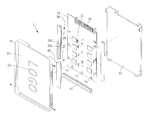
- FIG. 2 is a breakdown drawing of the preferred embodiment of the present invention.
- FIG. 3 is another breakdown drawing of the preferred embodiment of the present invention.
- FIG. 4 is a block diagram showing structural relations of elements according to the preferred embodiment of the present invention.
- the solid-state drive 1 includes a substrate 10 , a flash memory module 20 , at least one light-emitting portion and at least one light-guiding portion. More specifically, the solid-state drive 1 includes the substrate 10 , the flash memory module 20 , two the light-emitting portions 30 , 31 and two the light-guiding portions 40 , 41 .
- the substrate 10 has a transmit port 11 .
- the transmit port 11 may be a port for SATA (serial advanced technology attachment) or IDE (integrated development environment) in accordance with various scales of inserting slots of main boards.
- the transmit port 11 may be a port for USB (universal serial bus) so that the solid-state drive is portable.
- the flash memory module 20 is disposed on the substrate 10 , and the flash memory module 20 is electrically connected with the transmit port 11 . Compared with a memory cell of a conventional hard drive, a transmission speed of the flash memory module 20 is higher, and the solid-state drive is noiseless.
- the at least one light-emitting portion is disposed on the substrate 10 , and the at least one light-emitting portion is electrically connected with the transmit portion 11 .
- the at least one light-guiding portion at least partially covers the at least one light-emitting portion.
- the at least one light-guiding portion is translucent, and the at least one light-guiding portion can prevent a light emitted from the light-emitting portion from being emitted out directly and hurting human eyes. The light is softer after being reflected and absorbed by the at least one light-guiding portion.
- one of the light-emitting portions 30 is disposed on a circumferential side of the substrate 10 , and the light-guiding portion 40 covers the light-emitting portion 30 .
- the solid-state drive 1 further has a shell portion 50 , and the shell portion 50 includes two shell members 51 .
- the two shell members 51 cover two opposite side faces of the substrate 10 substantially perpendicular to a thickness direction thereof, and a light-transmittable portion 52 is formed on a circumferential side of the shell portion 50 .
- the light-guiding portion 40 is disposed between the two shell members 51 and corresponds to the light-transmittable portion 52 .
- the other light-emitting portion 31 is disposed at a center of one the side face of the substrate 10 substantially perpendicular to in a thickness direction thereof, and the light-guiding portion 41 covers the light-emitting portion 31 .
- the shell portion 50 covers the two side faces of the substrate 10 , and the shell portion 50 is formed with a light-transmittable portion 53 which corresponds to the light-guiding portion 41 .
- the light-transmittable portion 53 is a hollow portion having pictures and texts thereon (for example, trademarks), and the light from the light-guiding portion 41 projects through the light-transmittable portion 53 to show a picture-text effect.
- the light-transmittable portion may be a light-transmittable glass to protect the light-guiding portion and prevent dust from outside from entering the solid-state drive 1 . Therefore, the light projecting through a center and circumferential sides of the solid-state drive 1 makes the solid-state drive 1 more eye-catching, and the user can recognize, from expression of the light, a state of the solid-state drive 1 .
- the substrate 10 further includes a processing unit 60 .
- the processing unit 60 is electrically connected with the light-emitting portion 30 and able to control the light-emitting portion 30 (following is a description with the light-emitting portion 30 as an example, but the light-emitting portion 30 may be the light-emitting portion 31 as well).
- the processing unit 60 is electrically connected with a temperature sensing unit 61 , and the temperature sensing unit 61 can sense a temperature of at least one of the substrate 10 , the flash memory module 20 and the light-emitting portion 30 to produce a sensing signal.
- the processing unit 60 is able to control the light-emitting portion 30 (for example, a color or a frequency of light) according to the sensing signal.
- the light-emitting portion 30 includes a first light-emitting module 301 which is capable of emitting a first color and a second light-emitting module 302 which is capable of emitting a second color, and the first and second colors are different.
- the first color is blue
- the second color is red.
- the processing unit 60 is able to control at least one of the first light-emitting module 301 and the second light-emitting module 302 to be electrically communicable or incommunicable with the transmit port 11 . More specifically, when the temperature sensing unit 61 senses a relatively lower temperature, the first light-emitting module 301 is electrically communicable with the transmit port 11 , and the second light-emitting module 302 is electrically incommunicable with the transmit port 11 to make the light-guiding portion 40 emit a blue light; on the contrary, when the processing unit 61 senses a relatively higher temperature, the first light-emitting module 301 is electrically incommunicable with the transmit port 11 , and the second light-emitting module 302 is electrically communicable with the transmit port 11 to make the light-guiding portion 40 emit a red light. It is understandable that the processing unit 60 may be able to control the first light-emitting module 301 and the second light-emitting module 302 to emit stronger or weaker lights respectively
- the solid-state drive 1 further includes a transmission speed detecting unit 62 , and the transmission speed detecting unit 62 is electrically connected with the processing unit 60 and the transmit port 11 .
- the transmission speed detecting unit 62 is able to detect a transmission speed of the transmit port 11 to produce a detecting signal
- the processing unit 60 is able to control the light-emitting mode of the light-emitting portion 30 according to the detecting signal.
- the processing unit 60 when the transmission speed of the transmit port 11 is faster, the processing unit 60 is able to control the light-emitting portion 30 to flicker in a high frequency; on the contrary, when the transmission speed of the transmit port 11 is slower, the processing unit 60 is able to control the light-emitting portion 30 to flicker in a low frequency. Therefore, the user may know if there are any abnormal situations in the solid-state drive 1 through shining modes of the light-emitting portion 30 . It is understandable that the processing unit can control frequency of flicker via a preset program.
- the light-emitting modes for example, changes of colors or shining
- the light-emitting modes allow the user to know the state of the solid-state drive from an appearance of the solid-state drive to prevent the solid-state drive from being damaged due to abnormal situations.
- the solid-state drive further has the light-guiding portion to make the light emitted from the light-emitting portion softer so as to decrease the harm to human eyes.
Landscapes
- Physics & Mathematics (AREA)
- General Physics & Mathematics (AREA)
- Engineering & Computer Science (AREA)
- Optics & Photonics (AREA)
- Theoretical Computer Science (AREA)
- General Engineering & Computer Science (AREA)
- Microelectronics & Electronic Packaging (AREA)
- Stroboscope Apparatuses (AREA)
Abstract
Description
Claims (6)
Priority Applications (2)
| Application Number | Priority Date | Filing Date | Title |
|---|---|---|---|
| US14/725,569 US9512992B1 (en) | 2015-05-29 | 2015-05-29 | Solid-state drive |
| US15/256,986 US9668324B2 (en) | 2015-05-29 | 2016-09-06 | Solid-state drive |
Applications Claiming Priority (1)
| Application Number | Priority Date | Filing Date | Title |
|---|---|---|---|
| US14/725,569 US9512992B1 (en) | 2015-05-29 | 2015-05-29 | Solid-state drive |
Related Child Applications (1)
| Application Number | Title | Priority Date | Filing Date |
|---|---|---|---|
| US15/256,986 Division US9668324B2 (en) | 2015-05-29 | 2016-09-06 | Solid-state drive |
Publications (2)
| Publication Number | Publication Date |
|---|---|
| US20160348883A1 US20160348883A1 (en) | 2016-12-01 |
| US9512992B1 true US9512992B1 (en) | 2016-12-06 |
Family
ID=57398196
Family Applications (2)
| Application Number | Title | Priority Date | Filing Date |
|---|---|---|---|
| US14/725,569 Expired - Fee Related US9512992B1 (en) | 2015-05-29 | 2015-05-29 | Solid-state drive |
| US15/256,986 Expired - Fee Related US9668324B2 (en) | 2015-05-29 | 2016-09-06 | Solid-state drive |
Family Applications After (1)
| Application Number | Title | Priority Date | Filing Date |
|---|---|---|---|
| US15/256,986 Expired - Fee Related US9668324B2 (en) | 2015-05-29 | 2016-09-06 | Solid-state drive |
Country Status (1)
| Country | Link |
|---|---|
| US (2) | US9512992B1 (en) |
Families Citing this family (5)
| Publication number | Priority date | Publication date | Assignee | Title |
|---|---|---|---|---|
| US20170123136A1 (en) * | 2015-10-30 | 2017-05-04 | Avexir Technologies Corporation | Dynamic random access memory |
| US10429568B2 (en) * | 2015-10-30 | 2019-10-01 | Alson Technology Limited | Dynamic random access memory |
| US10073653B2 (en) | 2015-12-01 | 2018-09-11 | Alson Technology Limited | Solid state disk |
| US20170153961A1 (en) * | 2015-12-01 | 2017-06-01 | Avexir Technologies Corporation | Solid state disk |
| US20220415220A1 (en) * | 2021-06-24 | 2022-12-29 | BusyBox LLC | Wireless Status Sign System |
Citations (2)
| Publication number | Priority date | Publication date | Assignee | Title |
|---|---|---|---|---|
| US20080273300A1 (en) * | 2007-03-22 | 2008-11-06 | D-Link Corporation | Slot assembly of hard disk tower |
| TWI437573B (en) | 2010-07-30 | 2014-05-11 | Apacer Technology Inc | Solid - state hard disk module stack structure |
-
2015
- 2015-05-29 US US14/725,569 patent/US9512992B1/en not_active Expired - Fee Related
-
2016
- 2016-09-06 US US15/256,986 patent/US9668324B2/en not_active Expired - Fee Related
Patent Citations (2)
| Publication number | Priority date | Publication date | Assignee | Title |
|---|---|---|---|---|
| US20080273300A1 (en) * | 2007-03-22 | 2008-11-06 | D-Link Corporation | Slot assembly of hard disk tower |
| TWI437573B (en) | 2010-07-30 | 2014-05-11 | Apacer Technology Inc | Solid - state hard disk module stack structure |
Also Published As
| Publication number | Publication date |
|---|---|
| US20160374181A1 (en) | 2016-12-22 |
| US9668324B2 (en) | 2017-05-30 |
| US20160348883A1 (en) | 2016-12-01 |
Similar Documents
| Publication | Publication Date | Title |
|---|---|---|
| EP3091429A1 (en) | Solid-state drive | |
| US9668324B2 (en) | Solid-state drive | |
| US20160334559A1 (en) | Circuit module | |
| US9170353B2 (en) | Light emitting mirror structure | |
| CN204667882U (en) | Solid state hard disc | |
| WO2017155319A3 (en) | Display comprising sensing function, and electronic device comprising same | |
| US20160216434A1 (en) | Electronic device being able to show light graphics | |
| US20160226198A1 (en) | Power socket | |
| US20170142827A1 (en) | Electronic device and dynamic random access memory thereof | |
| TWM463420U (en) | Dynamic light emitting display device | |
| US9832297B2 (en) | Device including interface | |
| US9845935B1 (en) | Solid state disk | |
| US9016897B1 (en) | Inductive light source module | |
| US10429568B2 (en) | Dynamic random access memory | |
| TWI547038B (en) | Universal serial bus hub | |
| US9801280B2 (en) | Electronic device and circuit module thereof | |
| US9746172B1 (en) | Solid state disk | |
| US10209427B2 (en) | Electronic device | |
| TWI603361B (en) | Terminal device and remote monitoring control system having the same | |
| JP3183256U (en) | Transparent table | |
| US20160085345A1 (en) | Touch-sensing apparatus, touch system, and touch-detection method | |
| US20170123136A1 (en) | Dynamic random access memory | |
| TWI613668B (en) | Dual inline memory module with temperature-sensing scenario mode | |
| JP6565255B2 (en) | Light alarm device and lens thereof | |
| GB2544142A (en) | Electronic device and circuit module thereof |
Legal Events
| Date | Code | Title | Description |
|---|---|---|---|
| AS | Assignment |
Owner name: AVEXIR TECHNOLOGIES CORPORATION, TAIWAN Free format text: ASSIGNMENT OF ASSIGNORS INTEREST;ASSIGNOR:KUO, CHI-FEN;REEL/FRAME:035769/0476 Effective date: 20150528 |
|
| STCF | Information on status: patent grant |
Free format text: PATENTED CASE |
|
| AS | Assignment |
Owner name: ALSON TECHNOLOGY LIMITED, HONG KONG Free format text: ASSIGNMENT OF ASSIGNORS INTEREST;ASSIGNOR:AVEXIR TECHNOLOGIES CORPORATION;REEL/FRAME:042041/0849 Effective date: 20170405 |
|
| FEPP | Fee payment procedure |
Free format text: MAINTENANCE FEE REMINDER MAILED (ORIGINAL EVENT CODE: REM.); ENTITY STATUS OF PATENT OWNER: SMALL ENTITY |
|
| LAPS | Lapse for failure to pay maintenance fees |
Free format text: PATENT EXPIRED FOR FAILURE TO PAY MAINTENANCE FEES (ORIGINAL EVENT CODE: EXP.); ENTITY STATUS OF PATENT OWNER: SMALL ENTITY |
|
| STCH | Information on status: patent discontinuation |
Free format text: PATENT EXPIRED DUE TO NONPAYMENT OF MAINTENANCE FEES UNDER 37 CFR 1.362 |
|
| FP | Lapsed due to failure to pay maintenance fee |
Effective date: 20201206 |