US9507219B2 - Vertical alignment liquid crystal display device that has transistors with different switch-on resistance and method - Google Patents
Vertical alignment liquid crystal display device that has transistors with different switch-on resistance and method Download PDFInfo
- Publication number
- US9507219B2 US9507219B2 US14/938,887 US201514938887A US9507219B2 US 9507219 B2 US9507219 B2 US 9507219B2 US 201514938887 A US201514938887 A US 201514938887A US 9507219 B2 US9507219 B2 US 9507219B2
- Authority
- US
- United States
- Prior art keywords
- tft
- liquid crystal
- lcd device
- gray voltage
- pixel electrode
- Prior art date
- Legal status (The legal status is an assumption and is not a legal conclusion. Google has not performed a legal analysis and makes no representation as to the accuracy of the status listed.)
- Active
Links
- 239000004973 liquid crystal related substance Substances 0.000 title claims abstract description 52
- 238000000034 method Methods 0.000 title description 8
- 239000003990 capacitor Substances 0.000 claims abstract description 20
- 239000010409 thin film Substances 0.000 claims abstract description 4
- 239000000758 substrate Substances 0.000 description 7
- 238000010586 diagram Methods 0.000 description 3
- 230000005684 electric field Effects 0.000 description 2
- 230000003287 optical effect Effects 0.000 description 2
- 230000005540 biological transmission Effects 0.000 description 1
- 239000003086 colorant Substances 0.000 description 1
- 238000005286 illumination Methods 0.000 description 1
Images


Classifications
-
- G—PHYSICS
- G02—OPTICS
- G02F—OPTICAL DEVICES OR ARRANGEMENTS FOR THE CONTROL OF LIGHT BY MODIFICATION OF THE OPTICAL PROPERTIES OF THE MEDIA OF THE ELEMENTS INVOLVED THEREIN; NON-LINEAR OPTICS; FREQUENCY-CHANGING OF LIGHT; OPTICAL LOGIC ELEMENTS; OPTICAL ANALOGUE/DIGITAL CONVERTERS
- G02F1/00—Devices or arrangements for the control of the intensity, colour, phase, polarisation or direction of light arriving from an independent light source, e.g. switching, gating or modulating; Non-linear optics
- G02F1/01—Devices or arrangements for the control of the intensity, colour, phase, polarisation or direction of light arriving from an independent light source, e.g. switching, gating or modulating; Non-linear optics for the control of the intensity, phase, polarisation or colour
- G02F1/13—Devices or arrangements for the control of the intensity, colour, phase, polarisation or direction of light arriving from an independent light source, e.g. switching, gating or modulating; Non-linear optics for the control of the intensity, phase, polarisation or colour based on liquid crystals, e.g. single liquid crystal display cells
- G02F1/133—Constructional arrangements; Operation of liquid crystal cells; Circuit arrangements
- G02F1/1333—Constructional arrangements; Manufacturing methods
- G02F1/1343—Electrodes
- G02F1/134309—Electrodes characterised by their geometrical arrangement
-
- G—PHYSICS
- G02—OPTICS
- G02F—OPTICAL DEVICES OR ARRANGEMENTS FOR THE CONTROL OF LIGHT BY MODIFICATION OF THE OPTICAL PROPERTIES OF THE MEDIA OF THE ELEMENTS INVOLVED THEREIN; NON-LINEAR OPTICS; FREQUENCY-CHANGING OF LIGHT; OPTICAL LOGIC ELEMENTS; OPTICAL ANALOGUE/DIGITAL CONVERTERS
- G02F1/00—Devices or arrangements for the control of the intensity, colour, phase, polarisation or direction of light arriving from an independent light source, e.g. switching, gating or modulating; Non-linear optics
- G02F1/01—Devices or arrangements for the control of the intensity, colour, phase, polarisation or direction of light arriving from an independent light source, e.g. switching, gating or modulating; Non-linear optics for the control of the intensity, phase, polarisation or colour
- G02F1/13—Devices or arrangements for the control of the intensity, colour, phase, polarisation or direction of light arriving from an independent light source, e.g. switching, gating or modulating; Non-linear optics for the control of the intensity, phase, polarisation or colour based on liquid crystals, e.g. single liquid crystal display cells
- G02F1/133—Constructional arrangements; Operation of liquid crystal cells; Circuit arrangements
- G02F1/1333—Constructional arrangements; Manufacturing methods
- G02F1/1337—Surface-induced orientation of the liquid crystal molecules, e.g. by alignment layers
- G02F1/133707—Structures for producing distorted electric fields, e.g. bumps, protrusions, recesses, slits in pixel electrodes
-
- G—PHYSICS
- G02—OPTICS
- G02F—OPTICAL DEVICES OR ARRANGEMENTS FOR THE CONTROL OF LIGHT BY MODIFICATION OF THE OPTICAL PROPERTIES OF THE MEDIA OF THE ELEMENTS INVOLVED THEREIN; NON-LINEAR OPTICS; FREQUENCY-CHANGING OF LIGHT; OPTICAL LOGIC ELEMENTS; OPTICAL ANALOGUE/DIGITAL CONVERTERS
- G02F1/00—Devices or arrangements for the control of the intensity, colour, phase, polarisation or direction of light arriving from an independent light source, e.g. switching, gating or modulating; Non-linear optics
- G02F1/01—Devices or arrangements for the control of the intensity, colour, phase, polarisation or direction of light arriving from an independent light source, e.g. switching, gating or modulating; Non-linear optics for the control of the intensity, phase, polarisation or colour
- G02F1/13—Devices or arrangements for the control of the intensity, colour, phase, polarisation or direction of light arriving from an independent light source, e.g. switching, gating or modulating; Non-linear optics for the control of the intensity, phase, polarisation or colour based on liquid crystals, e.g. single liquid crystal display cells
- G02F1/133—Constructional arrangements; Operation of liquid crystal cells; Circuit arrangements
- G02F1/136—Liquid crystal cells structurally associated with a semi-conducting layer or substrate, e.g. cells forming part of an integrated circuit
- G02F1/1362—Active matrix addressed cells
- G02F1/136213—Storage capacitors associated with the pixel electrode
-
- G—PHYSICS
- G02—OPTICS
- G02F—OPTICAL DEVICES OR ARRANGEMENTS FOR THE CONTROL OF LIGHT BY MODIFICATION OF THE OPTICAL PROPERTIES OF THE MEDIA OF THE ELEMENTS INVOLVED THEREIN; NON-LINEAR OPTICS; FREQUENCY-CHANGING OF LIGHT; OPTICAL LOGIC ELEMENTS; OPTICAL ANALOGUE/DIGITAL CONVERTERS
- G02F1/00—Devices or arrangements for the control of the intensity, colour, phase, polarisation or direction of light arriving from an independent light source, e.g. switching, gating or modulating; Non-linear optics
- G02F1/01—Devices or arrangements for the control of the intensity, colour, phase, polarisation or direction of light arriving from an independent light source, e.g. switching, gating or modulating; Non-linear optics for the control of the intensity, phase, polarisation or colour
- G02F1/13—Devices or arrangements for the control of the intensity, colour, phase, polarisation or direction of light arriving from an independent light source, e.g. switching, gating or modulating; Non-linear optics for the control of the intensity, phase, polarisation or colour based on liquid crystals, e.g. single liquid crystal display cells
- G02F1/133—Constructional arrangements; Operation of liquid crystal cells; Circuit arrangements
- G02F1/136—Liquid crystal cells structurally associated with a semi-conducting layer or substrate, e.g. cells forming part of an integrated circuit
- G02F1/1362—Active matrix addressed cells
- G02F1/136286—Wiring, e.g. gate line, drain line
-
- G—PHYSICS
- G02—OPTICS
- G02F—OPTICAL DEVICES OR ARRANGEMENTS FOR THE CONTROL OF LIGHT BY MODIFICATION OF THE OPTICAL PROPERTIES OF THE MEDIA OF THE ELEMENTS INVOLVED THEREIN; NON-LINEAR OPTICS; FREQUENCY-CHANGING OF LIGHT; OPTICAL LOGIC ELEMENTS; OPTICAL ANALOGUE/DIGITAL CONVERTERS
- G02F1/00—Devices or arrangements for the control of the intensity, colour, phase, polarisation or direction of light arriving from an independent light source, e.g. switching, gating or modulating; Non-linear optics
- G02F1/01—Devices or arrangements for the control of the intensity, colour, phase, polarisation or direction of light arriving from an independent light source, e.g. switching, gating or modulating; Non-linear optics for the control of the intensity, phase, polarisation or colour
- G02F1/13—Devices or arrangements for the control of the intensity, colour, phase, polarisation or direction of light arriving from an independent light source, e.g. switching, gating or modulating; Non-linear optics for the control of the intensity, phase, polarisation or colour based on liquid crystals, e.g. single liquid crystal display cells
- G02F1/133—Constructional arrangements; Operation of liquid crystal cells; Circuit arrangements
- G02F1/136—Liquid crystal cells structurally associated with a semi-conducting layer or substrate, e.g. cells forming part of an integrated circuit
- G02F1/1362—Active matrix addressed cells
- G02F1/1368—Active matrix addressed cells in which the switching element is a three-electrode device
-
- G—PHYSICS
- G09—EDUCATION; CRYPTOGRAPHY; DISPLAY; ADVERTISING; SEALS
- G09G—ARRANGEMENTS OR CIRCUITS FOR CONTROL OF INDICATING DEVICES USING STATIC MEANS TO PRESENT VARIABLE INFORMATION
- G09G3/00—Control arrangements or circuits, of interest only in connection with visual indicators other than cathode-ray tubes
- G09G3/20—Control arrangements or circuits, of interest only in connection with visual indicators other than cathode-ray tubes for presentation of an assembly of a number of characters, e.g. a page, by composing the assembly by combination of individual elements arranged in a matrix no fixed position being assigned to or needed to be assigned to the individual characters or partial characters
- G09G3/34—Control arrangements or circuits, of interest only in connection with visual indicators other than cathode-ray tubes for presentation of an assembly of a number of characters, e.g. a page, by composing the assembly by combination of individual elements arranged in a matrix no fixed position being assigned to or needed to be assigned to the individual characters or partial characters by control of light from an independent source
- G09G3/36—Control arrangements or circuits, of interest only in connection with visual indicators other than cathode-ray tubes for presentation of an assembly of a number of characters, e.g. a page, by composing the assembly by combination of individual elements arranged in a matrix no fixed position being assigned to or needed to be assigned to the individual characters or partial characters by control of light from an independent source using liquid crystals
- G09G3/3611—Control of matrices with row and column drivers
- G09G3/3648—Control of matrices with row and column drivers using an active matrix
- G09G3/3659—Control of matrices with row and column drivers using an active matrix the addressing of the pixel involving the control of two or more scan electrodes or two or more data electrodes, e.g. pixel voltage dependant on signal of two data electrodes
-
- G—PHYSICS
- G02—OPTICS
- G02F—OPTICAL DEVICES OR ARRANGEMENTS FOR THE CONTROL OF LIGHT BY MODIFICATION OF THE OPTICAL PROPERTIES OF THE MEDIA OF THE ELEMENTS INVOLVED THEREIN; NON-LINEAR OPTICS; FREQUENCY-CHANGING OF LIGHT; OPTICAL LOGIC ELEMENTS; OPTICAL ANALOGUE/DIGITAL CONVERTERS
- G02F1/00—Devices or arrangements for the control of the intensity, colour, phase, polarisation or direction of light arriving from an independent light source, e.g. switching, gating or modulating; Non-linear optics
- G02F1/01—Devices or arrangements for the control of the intensity, colour, phase, polarisation or direction of light arriving from an independent light source, e.g. switching, gating or modulating; Non-linear optics for the control of the intensity, phase, polarisation or colour
- G02F1/13—Devices or arrangements for the control of the intensity, colour, phase, polarisation or direction of light arriving from an independent light source, e.g. switching, gating or modulating; Non-linear optics for the control of the intensity, phase, polarisation or colour based on liquid crystals, e.g. single liquid crystal display cells
- G02F1/133—Constructional arrangements; Operation of liquid crystal cells; Circuit arrangements
- G02F1/136—Liquid crystal cells structurally associated with a semi-conducting layer or substrate, e.g. cells forming part of an integrated circuit
- G02F1/1362—Active matrix addressed cells
- G02F1/13624—Active matrix addressed cells having more than one switching element per pixel
-
- G—PHYSICS
- G02—OPTICS
- G02F—OPTICAL DEVICES OR ARRANGEMENTS FOR THE CONTROL OF LIGHT BY MODIFICATION OF THE OPTICAL PROPERTIES OF THE MEDIA OF THE ELEMENTS INVOLVED THEREIN; NON-LINEAR OPTICS; FREQUENCY-CHANGING OF LIGHT; OPTICAL LOGIC ELEMENTS; OPTICAL ANALOGUE/DIGITAL CONVERTERS
- G02F2203/00—Function characteristic
- G02F2203/30—Gray scale
-
- G—PHYSICS
- G09—EDUCATION; CRYPTOGRAPHY; DISPLAY; ADVERTISING; SEALS
- G09G—ARRANGEMENTS OR CIRCUITS FOR CONTROL OF INDICATING DEVICES USING STATIC MEANS TO PRESENT VARIABLE INFORMATION
- G09G2300/00—Aspects of the constitution of display devices
- G09G2300/04—Structural and physical details of display devices
- G09G2300/0421—Structural details of the set of electrodes
- G09G2300/0426—Layout of electrodes and connections
-
- G—PHYSICS
- G09—EDUCATION; CRYPTOGRAPHY; DISPLAY; ADVERTISING; SEALS
- G09G—ARRANGEMENTS OR CIRCUITS FOR CONTROL OF INDICATING DEVICES USING STATIC MEANS TO PRESENT VARIABLE INFORMATION
- G09G2300/00—Aspects of the constitution of display devices
- G09G2300/04—Structural and physical details of display devices
- G09G2300/0439—Pixel structures
- G09G2300/0443—Pixel structures with several sub-pixels for the same colour in a pixel, not specifically used to display gradations
- G09G2300/0447—Pixel structures with several sub-pixels for the same colour in a pixel, not specifically used to display gradations for multi-domain technique to improve the viewing angle in a liquid crystal display, such as multi-vertical alignment [MVA]
-
- G—PHYSICS
- G09—EDUCATION; CRYPTOGRAPHY; DISPLAY; ADVERTISING; SEALS
- G09G—ARRANGEMENTS OR CIRCUITS FOR CONTROL OF INDICATING DEVICES USING STATIC MEANS TO PRESENT VARIABLE INFORMATION
- G09G2300/00—Aspects of the constitution of display devices
- G09G2300/08—Active matrix structure, i.e. with use of active elements, inclusive of non-linear two terminal elements, in the pixels together with light emitting or modulating elements
- G09G2300/0809—Several active elements per pixel in active matrix panels
- G09G2300/0842—Several active elements per pixel in active matrix panels forming a memory circuit, e.g. a dynamic memory with one capacitor
-
- G—PHYSICS
- G09—EDUCATION; CRYPTOGRAPHY; DISPLAY; ADVERTISING; SEALS
- G09G—ARRANGEMENTS OR CIRCUITS FOR CONTROL OF INDICATING DEVICES USING STATIC MEANS TO PRESENT VARIABLE INFORMATION
- G09G2310/00—Command of the display device
- G09G2310/02—Addressing, scanning or driving the display screen or processing steps related thereto
- G09G2310/0224—Details of interlacing
-
- G—PHYSICS
- G09—EDUCATION; CRYPTOGRAPHY; DISPLAY; ADVERTISING; SEALS
- G09G—ARRANGEMENTS OR CIRCUITS FOR CONTROL OF INDICATING DEVICES USING STATIC MEANS TO PRESENT VARIABLE INFORMATION
- G09G2310/00—Command of the display device
- G09G2310/02—Addressing, scanning or driving the display screen or processing steps related thereto
- G09G2310/0243—Details of the generation of driving signals
- G09G2310/0251—Precharge or discharge of pixel before applying new pixel voltage
-
- G—PHYSICS
- G09—EDUCATION; CRYPTOGRAPHY; DISPLAY; ADVERTISING; SEALS
- G09G—ARRANGEMENTS OR CIRCUITS FOR CONTROL OF INDICATING DEVICES USING STATIC MEANS TO PRESENT VARIABLE INFORMATION
- G09G2320/00—Control of display operating conditions
- G09G2320/02—Improving the quality of display appearance
- G09G2320/028—Improving the quality of display appearance by changing the viewing angle properties, e.g. widening the viewing angle, adapting the viewing angle to the view direction
-
- G—PHYSICS
- G09—EDUCATION; CRYPTOGRAPHY; DISPLAY; ADVERTISING; SEALS
- G09G—ARRANGEMENTS OR CIRCUITS FOR CONTROL OF INDICATING DEVICES USING STATIC MEANS TO PRESENT VARIABLE INFORMATION
- G09G3/00—Control arrangements or circuits, of interest only in connection with visual indicators other than cathode-ray tubes
- G09G3/20—Control arrangements or circuits, of interest only in connection with visual indicators other than cathode-ray tubes for presentation of an assembly of a number of characters, e.g. a page, by composing the assembly by combination of individual elements arranged in a matrix no fixed position being assigned to or needed to be assigned to the individual characters or partial characters
- G09G3/2007—Display of intermediate tones
- G09G3/2018—Display of intermediate tones by time modulation using two or more time intervals
- G09G3/2022—Display of intermediate tones by time modulation using two or more time intervals using sub-frames
- G09G3/2025—Display of intermediate tones by time modulation using two or more time intervals using sub-frames the sub-frames having all the same time duration
Definitions
- the present disclosure relates to a liquid crystal display device, and more particularly to a vertical alignment liquid crystal display (VA-LCD) device and a method for driving the VA-LCD device.
- VA-LCD vertical alignment liquid crystal display
- liquid crystal molecules in a liquid crystal display device emit no light themselves, illumination by a light source is necessary to display clear and sharp text and images.
- the liquid crystal display device can control the transmission of light beams emitted from a light source, so that the liquid crystal display device can display images.
- Twist-nematic type liquid crystal display (TN-LCD) devices while commonly used, are limited by a correspondingly narrow viewing angle, such that different colors are viewed from different angles.
- a multi-domain vertical alignment liquid crystal display (MVA-LCD) device and a patterned vertically aligned liquid crystal display (PVA-LCD) device have been developed. By disposing a plurality of “ ⁇ ” shaped protrusions or grooves on the inner surfaces of substrates, each pixel of the MVA-LCD device or PVA-LCD device is divided into a plurality of domains. The liquid crystal molecules of each domain are aligned at different angles, so as to widen the viewing angle of the LCD device.
- a long optical axis of the liquid crystal molecule has a refractive index different from that of a short optical axis of the liquid crystal molecule, generating color shift when viewed from different angles, thus the MVA-LCD device still has limited display quality.
- FIG. 1 is a schematic circuit diagram of a first embodiment of a VA-LCD device according to the present disclosure, the VA-LCD including a plurality of pixels.
- FIG. 2 is an enlarged view of a pixel of the VA-LCD device of FIG. 1 .
- FIG. 3 is a schematic side view of a pixel of a display panel of the VA-LCD device of FIG. 1 .
- FIG. 4 is a schematic plan view of the pixel of the display panel of the VA-LCD device of FIG. 3 .
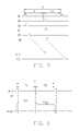
- FIG. 5 is a waveform graph of scanning signals of the VA-LCD device of FIG. 1 .
- FIG. 6 is a waveform graph of driving signals of the VA-LCD device of FIG. 1 .
- FIG. 7 is a flowchart of an exemplary method for driving the VA-LCD device of FIG. 1 .
- FIG. 8 is a schematic circuit of a second embodiment of a VA-LCD device according to the present disclosure.
- FIG. 9 is a waveform graph of driving signals of the VA-LCD device of FIG. 8 .
- FIG. 1 is a schematic circuit diagram of a first embodiment of a VA-LCD device 1 according to the present disclosure.
- the VA-LCD device 1 includes a display panel 11 , a data driving circuit 12 , and a scanning circuit 13 .
- the display panel 11 includes a plurality of parallel scan lines G 1 ⁇ Gj, and a plurality of data lines S 1 ⁇ Si parallel to each other and orthogonal to the scan lines G 1 ⁇ Gj.
- the scan lines G 1 ⁇ Gj and the data lines S 1 ⁇ Si cooperatively define a plurality of pixels 113 .
- FIG. 2 is an enlarged view of a pixel 113 of the VA-LCD device 1 of FIG. 1 .
- the data line Sm ⁇ 1 and the data line Sm together with the scan line Gn ⁇ 1 and the scan line Gn define the m ⁇ n'th pixel 113 , m and n represent any natural number, and 1 ⁇ m ⁇ i, 1 ⁇ n ⁇ j, so the m ⁇ n'th pixel 113 represents any pixel 113 of the VA-LCD device 1 .
- the m ⁇ n'th pixel 113 includes a first thin film transistor (TFT) 114 , a pixel electrode 152 , a common electrode 142 opposite to the pixel electrode 152 and a second TFT 115 .
- the common electrode 142 is electrically connected to a common voltage Vcom.
- a drain of the first TFT 114 is electrically connected to the pixel electrode 152 , a source thereof is electrically connected to the data line Sm ⁇ 1, and a gate thereof is electrically connected to the scan line Gn ⁇ 1.
- a drain of the second TFT 115 is electrically connected to the pixel electrode 152 , a source thereof is electrically connected to the common voltage Vcom, and a gate thereof is electrically connected to the scan line Gn.
- the pixel electrode 152 together with the common electrode 142 forms a liquid crystal capacitor 116 maintaining gray voltages.
- the electrical characteristic of the second TFT 115 is different from that of the first TFT 114 .
- a switch-on resistance of the second TFT 115 is greater than that of the first TFT 114 . While the same gate voltage is applied to the gates of the first TFT 114 and the second TFT 115 , and the same voltage is applied to the drains and the sources of the first TFT 114 and the second TFT 115 , current through the first TFT 114 is greater than that through the second TFT 115 .
- FIG. 3 shows a schematic side view of a pixel 113 of the display panel 11 of the VA-LCD device 1 of FIG. 1 .
- FIG. 4 shows a schematic plan view of the pixel 113 .
- the display panel 11 further includes a first substrate 14 , a second substrate 15 , and a liquid crystal layer 16 disposed between the first substrate 14 and the second substrate 15 .
- the common electrode 142 is disposed on a surface of the first substrate 14 that faces the liquid crystal layer 16 .
- a plurality of “ ⁇ ” shaped protrusions 143 are disposed on a surface of the common electrode 142 that faces the liquid crystal layer 16 .
- the pixel electrode 152 is disposed on a surface of the second substrate 15 that faces the liquid crystal layer 16 .
- a plurality of “ ⁇ ” shaped grooves 153 are formed in the pixel electrode 152 .
- Each “ ⁇ ” shaped groove 153 is disposed between two “ ⁇ ” shaped protrusions 143
- each “ ⁇ ” shaped protrusion 143 is disposed between two “ ⁇ ” shaped grooves 153 .
- FIG. 5 is a waveform graph of scanning signals of the VA-LCD device 1 of FIG. 1 .
- An interlacing scanning method is employed in the VA-LCD device 1 .
- one display frame time T of the VA-LCD device 1 is divided into two sequential substantially equal sub-display frame times T 1 , T 2 .
- the scanning circuit 13 sends scanning signals to the odd row scanning lines G 1 ⁇ Gj ⁇ 1 one after another; and in sub-display frame time T 2 , the scanning circuit 13 sends scanning signals to the even row scan lines G 2 ⁇ Gj one after another.
- the time between the scanning circuit 13 sending a scanning signal to the scan line Gn ⁇ 1 and sending a scanning signal to the scan line Gn is substantially half a display frame time T.
- FIG. 6 is a waveform graph of driving signals of the VA-LCD device 1 of FIG. 1 .
- FIG. 7 is a flow chart of an exemplary method for driving the VA-LCD device 1 . The method for driving the VA-LCD device 1 is described as below.
- step S 1 for the m ⁇ n'th pixel 113 , the scanning circuit 13 sends a scanning signal to the scan line Gn ⁇ 1.
- the scanning signal drives the first TFT 114 to be switched on.
- the data driving circuit 12 outputs a first gray voltage Vd 1 .
- the first gray voltage Vd 1 charges the liquid crystal capacitor 116 through the data line Sm and the first TFT 114 .
- the liquid crystal capacitor 116 maintains the first gray voltage Vd 1 .
- the electric field formed between the pixel electrode 152 and the common electrode 142 inclines to four different orientations because of the “ ⁇ ” shaped protrusions 143 and grooves 153 disposed in the pixel 113 and one protrusion 143 being disposed between every two grooves 153 .
- the declining electric field make liquid crystal molecules of the m ⁇ n'th pixel 113 align to four different orientations. A four-domain display is achieved.
- step S 2 half a display frame time T
- the scanning circuit 13 sends a scanning signal to the scan line Gn.
- the scanning signal switches the second TFT 115 on
- the liquid crystal capacitor 116 discharges through the second TFT 115 .
- the switch-on resistance of the second TFT 115 is greater than that of the first TFT 114
- the second TFT 115 is switched on by the scanning signal
- the liquid crystal capacitor 116 discharges incompletely.
- the second TFT 115 is switched off, the liquid crystal capacitor 116 maintains a second gray voltage Vd 2 lower than the first gray voltage Vd 1 .
- the m ⁇ n'th pixel 113 achieves an eight-domain display.
- the liquid crystal capacitor 116 maintains the first gray voltage Vd 1
- the liquid crystal capacitor 116 maintains the second gray voltage Vd 2 .
- the four-domain VA-LCD device 1 achieves an eight-domain display. Therefore, the VA-LCD device 1 reduces color shift, and achieves a higher display quality.
- FIG. 8 is a schematic circuit diagram of a VA-LCD device according to a second embodiment of the present disclosure, differing from the VA-LCD device 1 of the first embodiment in the further inclusion of an assistant scanning circuit 24 .
- the display panel 21 further includes a plurality of assistant scan lines Ga 1 ⁇ Gaj electrically connected to the assistant scanning circuit 24 .
- the electrical characteristic of the first TFT 214 and the second TFT 215 are the same.
- a gate of the second TFT 215 is electrically connected to a corresponding assistant scan line Gan.
- FIG. 9 is a waveform graph of driving signals of the VA-LCD device 2 of FIG. 8 .
- the scanning circuit 23 sends a first scanning signal Vg 1 to the scan line Gn, and switches the first TFT 214 on.
- the liquid crystal capacitor 216 maintains a first gray voltage Vd 1 .
- the assistant scanning circuit 24 sends a second scanning signal Vg 2 lower than the first scanning signal Vg 1 to the corresponding assistant scan line Gan.
- the second scanning signal Vg 2 switches the second TFT 215 on, and the liquid crystal capacitor 216 discharges through the second TFT 215 . Since the second scanning signal Vg 2 is lower than the first scanning signal Vg 1 , the liquid crystal capacitor 216 maintains a second gray voltage Vd 2 different from the first gray voltage Vd 1 .
- the four-domain VA-LCD device 2 can achieve an eight-domain display, such that the VA-LCD device 2 can reduce color shift and improve display quality.
- the electrical characteristics of the first TFT 214 and the second TFT 215 are the same, making the VA-LCD device 2 easier to fabricate.
- the VA-LCD device 1 , 2 can be any PVA-LCD device, or any MVA-LCD device.
- a threefold or fourfold interlacing scanning method can also be applied in the VA-LCD device 1 .
- the assistant scanning circuit 24 can also send a scanning signal having 1 ⁇ 3 display frame time delay to that sent by the scanning circuit 23 .
- the time between the assistant scanning circuit 24 sending a scanning signal and that sent by the scanning circuit 23 can be between about 1 ⁇ 4 display frame time to about 3 ⁇ 4 display frame time.
Landscapes
- Physics & Mathematics (AREA)
- Nonlinear Science (AREA)
- General Physics & Mathematics (AREA)
- Chemical & Material Sciences (AREA)
- Crystallography & Structural Chemistry (AREA)
- Engineering & Computer Science (AREA)
- Mathematical Physics (AREA)
- Optics & Photonics (AREA)
- Microelectronics & Electronic Packaging (AREA)
- Geometry (AREA)
- Computer Hardware Design (AREA)
- Theoretical Computer Science (AREA)
- Spectroscopy & Molecular Physics (AREA)
- Liquid Crystal (AREA)
- Power Engineering (AREA)
- Control Of Indicators Other Than Cathode Ray Tubes (AREA)
- Liquid Crystal Display Device Control (AREA)
Abstract
Description
Claims (14)
Priority Applications (1)
| Application Number | Priority Date | Filing Date | Title |
|---|---|---|---|
| US14/938,887 US9507219B2 (en) | 2008-05-16 | 2015-11-12 | Vertical alignment liquid crystal display device that has transistors with different switch-on resistance and method |
Applications Claiming Priority (6)
| Application Number | Priority Date | Filing Date | Title |
|---|---|---|---|
| CN200810067271 | 2008-05-16 | ||
| CN2008100672713A CN101581858B (en) | 2008-05-16 | 2008-05-16 | Vertical alignment liquid crystal display device and driving method thereof |
| CN200810067271.3 | 2008-05-16 | ||
| US12/454,450 US8692752B2 (en) | 2008-05-16 | 2009-05-18 | Vertical alignment liquid crystal display device and method for driving same |
| US14/185,342 US9217898B2 (en) | 2008-05-16 | 2014-02-20 | Vertical alignment liquid crystal display device and method for driving same |
| US14/938,887 US9507219B2 (en) | 2008-05-16 | 2015-11-12 | Vertical alignment liquid crystal display device that has transistors with different switch-on resistance and method |
Related Parent Applications (1)
| Application Number | Title | Priority Date | Filing Date |
|---|---|---|---|
| US14/185,342 Continuation US9217898B2 (en) | 2008-05-16 | 2014-02-20 | Vertical alignment liquid crystal display device and method for driving same |
Publications (2)
| Publication Number | Publication Date |
|---|---|
| US20160062195A1 US20160062195A1 (en) | 2016-03-03 |
| US9507219B2 true US9507219B2 (en) | 2016-11-29 |
Family
ID=41315809
Family Applications (4)
| Application Number | Title | Priority Date | Filing Date |
|---|---|---|---|
| US12/454,450 Active 2030-10-21 US8692752B2 (en) | 2008-05-16 | 2009-05-18 | Vertical alignment liquid crystal display device and method for driving same |
| US14/185,342 Active US9217898B2 (en) | 2008-05-16 | 2014-02-20 | Vertical alignment liquid crystal display device and method for driving same |
| US14/285,809 Active US9201274B2 (en) | 2008-05-16 | 2014-05-23 | Vertical alignment liquid crystal display device and method for driving same |
| US14/938,887 Active US9507219B2 (en) | 2008-05-16 | 2015-11-12 | Vertical alignment liquid crystal display device that has transistors with different switch-on resistance and method |
Family Applications Before (3)
| Application Number | Title | Priority Date | Filing Date |
|---|---|---|---|
| US12/454,450 Active 2030-10-21 US8692752B2 (en) | 2008-05-16 | 2009-05-18 | Vertical alignment liquid crystal display device and method for driving same |
| US14/185,342 Active US9217898B2 (en) | 2008-05-16 | 2014-02-20 | Vertical alignment liquid crystal display device and method for driving same |
| US14/285,809 Active US9201274B2 (en) | 2008-05-16 | 2014-05-23 | Vertical alignment liquid crystal display device and method for driving same |
Country Status (2)
| Country | Link |
|---|---|
| US (4) | US8692752B2 (en) |
| CN (1) | CN101581858B (en) |
Families Citing this family (18)
| Publication number | Priority date | Publication date | Assignee | Title |
|---|---|---|---|---|
| KR101590945B1 (en) * | 2009-11-17 | 2016-02-19 | 삼성디스플레이 주식회사 | Liquid crystal display |
| TWI469126B (en) * | 2012-09-05 | 2015-01-11 | Au Optronics Corp | Driving method of pixel of display panel |
| CN103353680B (en) | 2013-07-05 | 2015-08-19 | 京东方科技集团股份有限公司 | Liquid crystal pixel cells driving method and device |
| US20150109272A1 (en) * | 2013-10-22 | 2015-04-23 | Chenghung Chen | Array substrate and 3D display device |
| CN103531143B (en) * | 2013-10-22 | 2015-12-30 | 深圳市华星光电技术有限公司 | Array base palte and 3D display device |
| CN104298037B (en) * | 2014-10-20 | 2017-04-12 | 深圳市华星光电技术有限公司 | Glass panel and mask for manufacturing same |
| TWI564860B (en) * | 2015-09-17 | 2017-01-01 | 友達光電股份有限公司 | Driving method for display panel |
| CN105139821B (en) * | 2015-09-30 | 2018-03-13 | 深圳市华星光电技术有限公司 | A kind of array base palte and liquid crystal display |
| CN105118471B (en) | 2015-09-30 | 2018-01-09 | 深圳市华星光电技术有限公司 | Liquid crystal display panel and its driving method |
| KR102581368B1 (en) | 2016-07-07 | 2023-09-22 | 삼성디스플레이 주식회사 | Method of driving display panel and display apparatus for performing the same |
| CN106647084A (en) * | 2017-02-27 | 2017-05-10 | 深圳市华星光电技术有限公司 | Array substrate and display panel |
| CN106681040B (en) * | 2017-03-28 | 2019-11-05 | 京东方科技集团股份有限公司 | The driving method and driving device of display panel |
| TWI625578B (en) * | 2017-05-17 | 2018-06-01 | 友達光電股份有限公司 | Display panel and pixel circuit thereof |
| US10573257B2 (en) * | 2017-05-30 | 2020-02-25 | E Ink Corporation | Electro-optic displays |
| US11404013B2 (en) | 2017-05-30 | 2022-08-02 | E Ink Corporation | Electro-optic displays with resistors for discharging remnant charges |
| CN107703690B (en) * | 2017-09-26 | 2020-07-31 | 武汉华星光电技术有限公司 | Array substrate and display panel |
| CN108873524B (en) * | 2018-07-17 | 2021-01-26 | Tcl华星光电技术有限公司 | Display panel, method for improving performance of display panel and display device |
| CN109994087A (en) * | 2019-04-09 | 2019-07-09 | 深圳市华星光电技术有限公司 | Liquid crystal display device and its driving method |
Citations (11)
| Publication number | Priority date | Publication date | Assignee | Title |
|---|---|---|---|---|
| US6710825B2 (en) | 2000-08-11 | 2004-03-23 | Sharp Kabushiki Kaisha | LCD including pixel electrode with multiple sub-electrode portions |
| CN1540412A (en) | 2003-11-03 | 2004-10-27 | 友达光电股份有限公司 | Method for manufacturing vertical arranged direction type LCD of multi-domain, color filter base plate and polarizer |
| US20050030460A1 (en) * | 2003-06-10 | 2005-02-10 | Hee-Seob Kim | Liquid crystal display |
| US20060192747A1 (en) | 2003-04-08 | 2006-08-31 | Jong-Soo Yoon | Liquid crystal display apparatus |
| US20070013643A1 (en) * | 2005-07-18 | 2007-01-18 | Samsung Electronics Co., Ltd. | Liquid crystal display and driving method therefor |
| US20070018927A1 (en) * | 2005-07-20 | 2007-01-25 | Samsung Electronics Co., Ltd. | Liquid crystal display |
| US20070057257A1 (en) | 2005-09-15 | 2007-03-15 | Samsung Electronics Co., Ltd. | Liquid crystal display |
| WO2007040158A1 (en) | 2005-09-30 | 2007-04-12 | Sharp Kabushiki Kaisha | Liquid crystal display device and television receiver |
| CN101149548A (en) | 2007-11-06 | 2008-03-26 | 上海广电光电子有限公司 | Vertical orientation mode liquid crystal display device pixel circuit |
| US20080239182A1 (en) | 2007-04-02 | 2008-10-02 | Innolux Display Corp. | Multi-domain vertical alignment liquid crystal display |
| US20100103339A1 (en) | 2007-03-15 | 2010-04-29 | Fumikazu Shimoshikiryoh | Liquid crystal display device |
-
2008
- 2008-05-16 CN CN2008100672713A patent/CN101581858B/en active Active
-
2009
- 2009-05-18 US US12/454,450 patent/US8692752B2/en active Active
-
2014
- 2014-02-20 US US14/185,342 patent/US9217898B2/en active Active
- 2014-05-23 US US14/285,809 patent/US9201274B2/en active Active
-
2015
- 2015-11-12 US US14/938,887 patent/US9507219B2/en active Active
Patent Citations (12)
| Publication number | Priority date | Publication date | Assignee | Title |
|---|---|---|---|---|
| US6710825B2 (en) | 2000-08-11 | 2004-03-23 | Sharp Kabushiki Kaisha | LCD including pixel electrode with multiple sub-electrode portions |
| US20060192747A1 (en) | 2003-04-08 | 2006-08-31 | Jong-Soo Yoon | Liquid crystal display apparatus |
| US20050030460A1 (en) * | 2003-06-10 | 2005-02-10 | Hee-Seob Kim | Liquid crystal display |
| CN1540412A (en) | 2003-11-03 | 2004-10-27 | 友达光电股份有限公司 | Method for manufacturing vertical arranged direction type LCD of multi-domain, color filter base plate and polarizer |
| US20070013643A1 (en) * | 2005-07-18 | 2007-01-18 | Samsung Electronics Co., Ltd. | Liquid crystal display and driving method therefor |
| US20070018927A1 (en) * | 2005-07-20 | 2007-01-25 | Samsung Electronics Co., Ltd. | Liquid crystal display |
| US20070057257A1 (en) | 2005-09-15 | 2007-03-15 | Samsung Electronics Co., Ltd. | Liquid crystal display |
| WO2007040158A1 (en) | 2005-09-30 | 2007-04-12 | Sharp Kabushiki Kaisha | Liquid crystal display device and television receiver |
| US20090273743A1 (en) | 2005-09-30 | 2009-11-05 | Daiichi Sawabe | Liquid Crystal Display and Television Receiver |
| US20100103339A1 (en) | 2007-03-15 | 2010-04-29 | Fumikazu Shimoshikiryoh | Liquid crystal display device |
| US20080239182A1 (en) | 2007-04-02 | 2008-10-02 | Innolux Display Corp. | Multi-domain vertical alignment liquid crystal display |
| CN101149548A (en) | 2007-11-06 | 2008-03-26 | 上海广电光电子有限公司 | Vertical orientation mode liquid crystal display device pixel circuit |
Also Published As
| Publication number | Publication date |
|---|---|
| US9201274B2 (en) | 2015-12-01 |
| US9217898B2 (en) | 2015-12-22 |
| US8692752B2 (en) | 2014-04-08 |
| US20160062195A1 (en) | 2016-03-03 |
| US20090284674A1 (en) | 2009-11-19 |
| US20140253837A1 (en) | 2014-09-11 |
| CN101581858B (en) | 2012-02-08 |
| US20140168561A1 (en) | 2014-06-19 |
| CN101581858A (en) | 2009-11-18 |
Similar Documents
| Publication | Publication Date | Title |
|---|---|---|
| US9507219B2 (en) | Vertical alignment liquid crystal display device that has transistors with different switch-on resistance and method | |
| US8207923B2 (en) | Liquid crystal display panel, method for driving the same, and liquid crystal display apparatus using the same | |
| US8487847B2 (en) | Liquid crystal display and method of manufacturing the same | |
| US8228274B2 (en) | Liquid crystal panel, liquid crystal display, and driving method thereof | |
| US6166714A (en) | Displaying device | |
| US8194201B2 (en) | Display panel and liquid crystal display including the same | |
| TWI397734B (en) | Liquid crystal display and driving method thereof | |
| US20080259234A1 (en) | Liquid crystal display device and method for driving same | |
| US20090262056A1 (en) | Liquid crystal display panel with color washout improvement and applications of same | |
| US7710139B2 (en) | Electro-optical device and electronic apparatus | |
| GB2421832A (en) | Liquid crystal display device using in-plane switching mode | |
| US20050088386A1 (en) | [liquid crystal display panel and driving circuit thereof] | |
| US8581819B2 (en) | Apparatus and method for driving liquid crystal display device | |
| EP1187091A2 (en) | Method of driving scanning lines of a active matrix liquid crystal device | |
| US7928943B2 (en) | Liquid crystal display | |
| US20070070014A1 (en) | Pixel structure of liquid crystal device and driving method thereof | |
| US20060044238A1 (en) | OCB mode LCD and method for driving the same | |
| US20060145988A1 (en) | Active matrix liquid crystal display | |
| US7697081B2 (en) | Pixel structure of liquid crystal display comprising V-shaped drain and source electrodes and method for activating a state transition of a liquid crystal layer | |
| US6909412B2 (en) | Method for driving liquid crystal of thin film transistor liquid crystal display | |
| US11209708B2 (en) | Display device | |
| KR100932553B1 (en) | Analog sampling circuit for liquid crystal display and its driving method | |
| CN101304032B (en) | Pixel structure and drive method thereof | |
| JP2007206181A (en) | Liquid crystal display device | |
| KR20020057406A (en) | liquid crystal display apparatus for static image and method for improving its aperture ratio |
Legal Events
| Date | Code | Title | Description |
|---|---|---|---|
| AS | Assignment |
Owner name: INNOLUX CORPORATION, TAIWAN Free format text: ASSIGNMENT OF ASSIGNORS INTEREST;ASSIGNORS:CHANG, YUEH-PING;HUNG, CHAO-YI;REEL/FRAME:037019/0807 Effective date: 20140217 |
|
| STCF | Information on status: patent grant |
Free format text: PATENTED CASE |
|
| MAFP | Maintenance fee payment |
Free format text: PAYMENT OF MAINTENANCE FEE, 4TH YEAR, LARGE ENTITY (ORIGINAL EVENT CODE: M1551); ENTITY STATUS OF PATENT OWNER: LARGE ENTITY Year of fee payment: 4 |
|
| MAFP | Maintenance fee payment |
Free format text: PAYMENT OF MAINTENANCE FEE, 8TH YEAR, LARGE ENTITY (ORIGINAL EVENT CODE: M1552); ENTITY STATUS OF PATENT OWNER: LARGE ENTITY Year of fee payment: 8 |