US9501095B2 - Display device - Google Patents
Display device Download PDFInfo
- Publication number
- US9501095B2 US9501095B2 US14/114,667 US201114114667A US9501095B2 US 9501095 B2 US9501095 B2 US 9501095B2 US 201114114667 A US201114114667 A US 201114114667A US 9501095 B2 US9501095 B2 US 9501095B2
- Authority
- US
- United States
- Prior art keywords
- display device
- adhesive member
- double
- panel
- chassis
- Prior art date
- Legal status (The legal status is an assumption and is not a legal conclusion. Google has not performed a legal analysis and makes no representation as to the accuracy of the status listed.)
- Active, expires
Links
- 239000000853 adhesive Substances 0.000 claims abstract description 96
- 230000001070 adhesive effect Effects 0.000 claims abstract description 95
- 239000011347 resin Substances 0.000 abstract description 77
- 229920005989 resin Polymers 0.000 abstract description 77
- 239000000463 material Substances 0.000 abstract 1
- 230000000694 effects Effects 0.000 description 11
- 230000006866 deterioration Effects 0.000 description 7
- 238000009423 ventilation Methods 0.000 description 6
- 238000000034 method Methods 0.000 description 4
- 230000002093 peripheral effect Effects 0.000 description 3
- 239000002390 adhesive tape Substances 0.000 description 2
- 230000005540 biological transmission Effects 0.000 description 2
- 230000001747 exhibiting effect Effects 0.000 description 2
- 239000004973 liquid crystal related substance Substances 0.000 description 2
- 239000012790 adhesive layer Substances 0.000 description 1
- 230000000903 blocking effect Effects 0.000 description 1
- 230000003247 decreasing effect Effects 0.000 description 1
- 238000012986 modification Methods 0.000 description 1
- 230000004048 modification Effects 0.000 description 1
- 230000010287 polarization Effects 0.000 description 1
- 125000006850 spacer group Chemical group 0.000 description 1
- 239000000758 substrate Substances 0.000 description 1
Images


Classifications
-
- G—PHYSICS
- G06—COMPUTING; CALCULATING OR COUNTING
- G06F—ELECTRIC DIGITAL DATA PROCESSING
- G06F1/00—Details not covered by groups G06F3/00 - G06F13/00 and G06F21/00
- G06F1/16—Constructional details or arrangements
- G06F1/1601—Constructional details related to the housing of computer displays, e.g. of CRT monitors, of flat displays
-
- G—PHYSICS
- G06—COMPUTING; CALCULATING OR COUNTING
- G06F—ELECTRIC DIGITAL DATA PROCESSING
- G06F1/00—Details not covered by groups G06F3/00 - G06F13/00 and G06F21/00
- G06F1/16—Constructional details or arrangements
- G06F1/1613—Constructional details or arrangements for portable computers
- G06F1/1633—Constructional details or arrangements of portable computers not specific to the type of enclosures covered by groups G06F1/1615 - G06F1/1626
- G06F1/1656—Details related to functional adaptations of the enclosure, e.g. to provide protection against EMI, shock, water, or to host detachable peripherals like a mouse or removable expansions units like PCMCIA cards, or to provide access to internal components for maintenance or to removable storage supports like CDs or DVDs, or to mechanically mount accessories
-
- H—ELECTRICITY
- H05—ELECTRIC TECHNIQUES NOT OTHERWISE PROVIDED FOR
- H05K—PRINTED CIRCUITS; CASINGS OR CONSTRUCTIONAL DETAILS OF ELECTRIC APPARATUS; MANUFACTURE OF ASSEMBLAGES OF ELECTRICAL COMPONENTS
- H05K7/00—Constructional details common to different types of electric apparatus
- H05K7/14—Mounting supporting structure in casing or on frame or rack
Definitions
- the present invention relates to a display device such as a liquid crystal display device, an organic EL display, or the like, for example.
- the protection panel is fixed to a chassis or the like via a double-sided tape, and a spatial gap is provided between the protection panel and the display panel.
- This spatial gap prevents display failures on the display panel caused due to a pressure applied to the protection panel through blocking the influence of flexure of the protection panel.
- a slit is provided to the double-sided tape used for fixing the protection panel so that the spatial gap is not in a sealed state.
- FIG. 22 is a fragmented perspective view showing a touch screen display device of the related technique.
- FIG. 23 is a plan view showing an adhesive member in the touch screen display device of FIG. 22 .
- the touch screen display device of the related technique includes a display panel 610 , a touch panel 630 , and an adhesive member 650 .
- a display panel 610 an effective display area DA and a peripheral area PA surrounding the effective display area DA are defined, and a flexible substrate 612 is connected thereto.
- the adhesive member 650 is interposed between the display panel 610 and the touch panel 630 in the peripheral area PA defined in the display panel 610 to bond those to each other.
- a polarization film 617 is laminated.
- a ventilation path 657 is formed in the vicinity of each of the centers (B part) of two long sides of the peripheral area PA of the display panel 610 . Air is flown in or out to/from the space between the touch panel 630 and the display panel 610 via the ventilation path 657 .
- the adhesive member 650 includes first and second adhesive tapes 653 and 655 .
- the ventilation path 657 is formed by a protruded portion and a recessed portion engaged with each other formed in the ends of each of the first and the second adhesive tapes 653 and 655 , and forms a shape bent at four positions.
- the air pressure of the space surrounded by the adhesive member 650 changes according to the external pressure of the display device by the ventilation path 657 . Further, the bent parts of the complicated-shaped ventilation 657 confine foreign matters so as to prevent intrusion of the foreign matters to the inside of the display device.
- Patent Document 2 discloses a display device in which a complicated-shaped ventilation path is formed by processing an adhesive member of a touch panel.
- Patent Document 3 discloses a display device of a complicated structure in which a dust-proof spacer is attached to a touch panel.
- Patent Document 1 Japanese Unexamined Patent Publication 2007-293810
- Patent Document 2 Registered Utility Model No. 3159189
- Patent Document 3 Japanese Unexamined Patent Publication 2005-242423
- the display device having the structure where the protection panel such as a touch panel is fixed to a resin chassis via a double-sided tape
- image quality failures including distortion of the images and deterioration of the image quality are generated when a foreign matter enters from a gap generated at the position where the double-sided tape is pasted or a gap generated due to the thickness of the double-sided tape.
- the shape of the double-sided tape is made complicated for preventing the foreign matter from entering as a countermeasure, the cost for the double-sided tape is increased because the amount of the double-sided tape to be wasted is increased.
- to paste the complicated-shaped double-sided tape is extremely bad in terms of the workability. This issue has become serious in accordance with recent increase in the scale of the display devices in particular.
- the display device is characterized to include: a display panel; a protection panel placed on a display surface of the display panel via a space; a chassis for housing the display panel; and an adhesive member for fixing the protection panel to the chassis, wherein:
- the wall corresponding to an upper level of the step is provided in the region where the end portion of the adhesive member is placed so as to spatially separate the adhesive member and the display panel. Therefore, it is possible to prevent intrusion of the foreign matter from the gap formed between the adhesive member and the chassis generated when the structure is simplified.
- FIG. 1 is an overall perspective view showing a display device according to a first exemplary embodiment of the present invention
- FIG. 2 is a fragmented perspective view showing the display device of FIG. 1 ;
- FIG. 3 is an elevational view showing a state where a touch panel is omitted from the display device of FIG. 1 ;
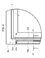
- FIG. 4 is a detailed view showing A part of FIG. 3 ;
- FIG. 5 is a sectional view taken along a line A 1 -A 1 of FIG. 4 , which shows the state where the touch panel is added;
- FIG. 6 is an elevational view showing a state where a touch panel is omitted from a display device according to a second exemplary embodiment of the present invention.
- FIG. 7 is a detailed view showing B part of FIG. 6 ;
- FIG. 8 is a sectional view taken along a line B 1 -B 1 of FIG. 7 , which shows the state where the touch panel is added;
- FIG. 9 is a sectional view taken along a line B 2 -B 2 of FIG. 7 , which shows the state where the touch panel is added;
- FIG. 10 is an elevational view showing a state where a touch panel is omitted from a display device according to a third exemplary embodiment of the present invention.
- FIG. 11 is a detailed view showing C part of FIG. 10 ;
- FIG. 12 is a sectional view taken along a line C 1 -C 1 of FIG. 11 , which shows the state where the touch panel is added;
- FIG. 13 is a sectional view taken along a line C 2 -C 2 of FIG. 11 , which shows the state where the touch panel is added;
- FIG. 14 is an elevational view showing a state where a touch panel is omitted from a display device according to a fourth exemplary embodiment of the present invention.
- FIG. 15 is a detailed view showing D part of FIG. 14 ;
- FIG. 16 is a sectional view taken along a line D 1 -D 1 of FIG. 15 , which shows the state where the touch panel is added;
- FIG. 17 is a sectional view taken along a line D 2 -D 2 of FIG. 15 , which shows the state where the touch panel is added;
- FIG. 18 is an elevational view showing a state where a touch panel is omitted from a display device according to a fifth exemplary embodiment of the present invention.
- FIG. 19 is a detailed view showing E part of FIG. 18 ;
- FIG. 20 is a sectional view taken along a line E 1 -E 1 of FIG. 19 , which shows the state where the touch panel is added;
- FIG. 21 is a sectional view taken along a line E 2 -E 2 of FIG. 19 , which shows the state where the touch panel is added;
- FIG. 22 is a fragmented perspective view showing a touch screen display device according to a related technique.
- FIG. 23 is a plan view showing an adhesive member of the touch screen display device of FIG. 22 .
- FIG. 1 is an overall perspective view showing the display device of a first exemplary embodiment according to the present invention.
- FIG. 2 is a fragmented perspective view showing the display device of FIG. 1 .
- FIG. 3 is an elevational view showing a state where a touch panel is omitted from the display device of FIG. 1 .
- FIG. 4 is a detailed view showing A part of FIG. 3 .
- FIG. 5 is a sectional view taken along a line A 1 -A 1 of FIG. 4 , which shows the state where the touch panel is added.
- the display device includes: a display device 1 as a display panel; a touch panel 2 as a protection panel placed on the display surface of the display device 1 via a space 8 ; a resin chassis 3 a as a chassis for housing the display device 1 ; and double-sided tapes 4 a and 40 a as an adhesive member for fixing the touch panel 2 to the resin chassis 3 a .
- steps 31 a and 32 a of height equal to or less than the thickness of the double-sided tapes 4 a and 40 a are provided on the top surface of the resin chassis 3 a opposing to the touch panel 2 .
- the double-sided tapes 4 a and 40 a are placed in the regions to be the lower levels of the steps 31 a and 32 a .
- a wall (step 31 a ) corresponding to the upper level of the steps 31 a and 32 a is provided to spatially separate the double-sided tapes 4 a , 40 a and the display device 1 .
- the display device according to the first exemplary embodiment it is possible to prevent intrusion of a foreign matter from a gap between the double-sided tapes 4 a , 40 a and the resin chassis 3 a generated by simplifying the structure.
- the display device includes: the display device 1 as the display panel; the resin chassis 3 a as the chassis 3 for housing the display device 1 ; the touch panel 2 as the protection panel for covering the display device 1 via the space 8 ; the double-sided tapes 4 a , 40 a as the adhesive member for fixing the touch panel 2 to the rim of the resin chassis 3 a ; and the steps 31 a , 32 a provided at least one of the mutually opposing faces of the resin chassis 3 a and the touch panel 2 , which are protruded portions for forming a clearance 9 a to be a path for the air of inside and outside of the space 8 .
- the steps 31 a and 32 a are provided to the resin chassis 3 a , which are a first protruded plane of height lower than the thickness of the double-sided tapes 4 a and 40 a .
- the double-sided tapes 4 a and 40 a have an adhesive layer constituted with an adhesive agent or the like on both of the top and back sides.
- the clearance 9 a between the steps 31 a , 32 a and the touch panel 2 is narrower than the gap between the resin chassis 3 a and the touch panel 2 formed by the existence of the double-sided tapes 4 a , 40 a , so that it functions to block intrusion of the foreign matter.
- the display device includes: the display device 1 ; the touch panel 2 ; the resin chassis 3 a into which the display device 1 is fitted; and the double-sided tapes 4 a , 40 a for fixing the touch panel 2 to the resin chassis 3 a .
- the double-sided tapes 4 a , 40 a are pasted.
- the step 31 a of the height equal to or less than the thickness of the double-sided tapes 4 a , 40 a is provided.
- the touch panel 2 is fixed to the resin chassis 3 a via the double-sided tapes 4 a , 40 a.
- the structure of the side to which the double-sided tape 40 a is pasted will be described herein.
- the step 32 a of the height equal to or less than the thickness of the double-sided tape 40 a is provided on the resin chassis 3 a between the double-sided tape 40 a and the display device 1 .
- the clearance 9 a formed between the step 32 a and the touch panel 2 is set to be equal to or less than the size of the assumed foreign matter.
- a slit 5 a formed by the end portion 41 a of the double-sided tape 40 a and the step 32 a of the resin chassis 3 a forms a shape isolated from the inner side of the display device. Further, through employing the same structure, a slit forming a shape isolated from the inner side of the display device is formed also with the structure on the side where the double-sided tape 4 a is pasted.
- the shape of the double-sided tapes 4 a , 40 a can be simplified, it is possible to reduce the unnecessary part of the double-sided tape and design the layout efficiently in terms of the area. Therefore, the structure capable of suppressing intrusion of the foreign matters into the inside of the display device can be achieved at a low cost. Furthermore, since the clearance 9 a between the resin chassis 3 a and the touch panel 2 can be set according to the size of the assumed foreign matter without depending on the thickness of the double-sided tapes 4 a , 40 a , it is possible to select the double-sided tape which is high in the adhesive strength or is not easily influenced by the unevenness on the resin chassis 3 a . Therefore, the fixing strength of the touch panel 2 can be increased.
- FIG. 6 is an elevational view showing a state where a touch panel is omitted from a display device according to a second exemplary embodiment of the present invention.
- FIG. 7 is a detailed view showing B part of FIG. 6 .
- FIG. 8 is a sectional view taken along a line B 1 -B 1 of FIG. 7 , which shows the state where the touch panel is added.
- FIG. 9 is a sectional view taken along a line B 2 -B 2 of FIG. 7 , which shows the state where the touch panel is added.
- Steps 31 b and 32 b of the display device according to the second exemplary embodiment are provided on a resin chassis 3 b , which are a first protruded plane of the height lower than the thickness of double-sided tapes 4 a and 40 a .
- a slit 5 b for capturing a foreign matter entering inside a space 8 is provided.
- the slit 5 b forms a shape reaching from the periphery of an end portion 41 b of double-sided tapes 4 b , 40 b to the space 8 .
- the display device of the second exemplary embodiment includes: the display device 1 ; the touch panel 2 ; the resin chassis 3 b into which the display device 1 is fitted; and the double-sided tapes 4 b , 40 b for fixing the touch panel 2 to the resin chassis 3 b .
- the double-sided tapes 4 b , 40 b are pasted.
- the step 31 b of the height equal to or less than the thickness of the double-sided tapes 4 b , 40 b is provided.
- the touch panel 2 is fixed to the resin chassis 3 b via the double-sided tapes 4 b , 40 b.
- the structure of the side to which the double-sided tape 40 b is pasted will be described herein.
- the step 32 b of the height equal to or less than the thickness of the double-sided tape 40 b is provided on the resin chassis 3 b between the double-sided tape 40 b and the display device 1 .
- a clearance 9 b formed between the step 32 b and the touch panel 2 is set to be equal to or less than the size of the assumed foreign matter.
- a slit 5 b formed by the end portion 41 b of the double-sided tape 40 b and the step 32 b of the resin chassis 3 b forms a shape that is not in a straight form. Further, through employing the same structure, a slit forming a shape that is not in a straight form can be formed also with the structure on the side where the double-sided tape 4 b is pasted.
- the long and nonlinear slit 5 b is formed by the end portion 41 b of the double-sided tape 40 b and the resin chassis 3 b to which the steps 31 b , 32 b are attached, so that a foreign matter that is about to enter the display device from outside can be captured within the slit 5 b .
- intrusion of the foreign matter into the inside of the display device can be suppressed, so that it is possible to prevent the image quality failures including the distortion of the image and deterioration of the image quality which may be caused thereby.
- the shape of the double-sided tapes 4 b , 40 b can be simplified, it is possible to reduce the unnecessary part of the double-sided tape and design the layout efficiently in terms of the area. Therefore, the structure capable of suppressing intrusion of the foreign matters into the inside of the display device can be achieved at a low cost.
- Other structures, operations, and effects of the display device according to the second exemplary embodiment are the same as those of the first exemplary embodiment.
- FIG. 10 is an elevational view showing a state where a touch panel is omitted from a display device according to a third exemplary embodiment of the present invention.
- FIG. 11 is a detailed view showing C part of FIG. 10 .
- FIG. 12 is a sectional view taken along a line C 1 -C 1 of FIG. 11 , which shows the state where the touch panel is added.
- FIG. 13 is a sectional view taken along a line C 2 -C 2 of FIG. 11 , which shows the state where the touch panel is added.
- FIG. 10 is an elevational view showing a state where a touch panel is omitted from a display device according to a third exemplary embodiment of the present invention.
- FIG. 11 is a detailed view showing C part of FIG. 10 .
- FIG. 12 is a sectional view taken along a line C 1 -C 1 of FIG. 11 , which shows the state where the touch panel is added.
- FIG. 13 is a sectional view taken along a line C 2
- Steps 31 c and 32 c of the display device according to the third exemplary embodiment are provided on a resin chassis 3 c , which are a first protruded plane of the height lower than the thickness of double-sided tapes 4 c and 40 c .
- a slit 5 c for capturing a foreign matter entering inside a space 8 and a double-sided tape 6 c as an adhesive member for capturing a foreign matter entering inside the space 8 are provided.
- One of the faces of the double-sided tape 6 c is bonded to the resin chassis 3 c , and the other face thereof is used as the adhesive member.
- the display device of the third exemplary embodiment includes: the display device 1 ; the touch panel 2 ; the resin chassis 3 c into which the display device 1 is fitted; the double-sided tapes 4 c , 40 c for fixing the touch panel 2 to the resin chassis 3 c ; and the double-sided tape 6 c for fixing the display device 1 to the resin chassis 3 c .
- the double-sided tapes 4 c , 40 c are pasted.
- the step 31 c of the height equal to or less than the thickness of the double-sided tapes 4 c , 40 c is provided.
- the touch panel 2 is fixed to the resin chassis 3 c via the double-sided tapes 4 c , 40 c.
- the structure of the side to which the double-sided tape 40 c is pasted will be described herein.
- the step 32 c of the height equal to or less than the thickness of the double-sided tape 40 c is provided on the resin chassis 3 c between the double-sided tape 40 c and the display device 1 .
- a clearance 9 c formed between the step 32 c and the touch panel 2 is set to be equal to or less than the size of the assumed foreign matter.
- a slit 5 c formed by the end portion 41 c of the double-sided tape 40 c and the resin chassis 3 c forms a shape having two corners.
- a rib 7 c for guiding the fixation of the display device 1 is provided to the resin chassis 3 c .
- the end portion 41 c of the double-sided tape 40 c is the position opposing to the rib 7 c .
- the double-sided tape 6 c is extended to a space 61 c formed between the resin chassis 3 c and the display device 1 .
- As the double-sided tape 6 c it is also possible to use a type exhibiting the light-shielding property. Further, through employing the same structure, a slit forming a shape that is not in a straight form can be formed and the double-sided tape 6 c is extended also with the structure on the side where the double-sided tape 4 c is pasted.
- the double-sided tape 6 c provided within the display device captures the foreign matter entered inside the display device from outside. Thereby, intrusion of the foreign matter into the inside of the display device can be suppressed, so that it is possible to prevent the image quality failures including the distortion of the image and deterioration of the image quality. Further, through using the type exhibiting the light-shielding property for the double-sided tape 6 c , it is possible to suppress transmission of the unnecessary light into the space formed inside the display device, such as the light transmitting through the resin chassis 3 c .
- the steps 31 c and 32 c suppress intrusion of the foreign matter to the inside the display device and the double-sided tape 6 c pasted to the inside captures the foreign matter that is about to enter, so that intrusion of the foreign matter onto the display area can be prevented. Further, through suppressing the transmission of the unnecessary light into the space formed inside the display device, deterioration of the display quality can be prevented.
- Other structures, operations, and effects of the display device according to the third exemplary embodiment are the same as those of the first to second exemplary embodiments.
- FIG. 14 is an elevational view showing a state where a touch panel is omitted from a display device according to a fourth exemplary embodiment of the present invention.
- FIG. 15 is a detailed view showing D part of FIG. 14 .
- FIG. 16 is a sectional view taken along a line D 1 -D 1 of FIG. 15 , which shows the state where the touch panel is added.
- FIG. 17 is a sectional view taken along a line D 2 -D 2 of FIG. 15 , which shows the state where the touch panel is added.
- Steps 31 d and 32 d of the display device according to a fourth exemplary embodiment are provided on a resin chassis 3 d , which are a first protruded plane of the height lower than the thickness of double-sided tapes 4 d and 40 d .
- a slit 5 d for capturing a foreign matter entering inside a space 8 and a double-sided tape 6 d as an adhesive member for capturing a foreign matter entering inside the space 8 are provided.
- a step 33 d is provided on the outside of the touch panel 2 of the resin chassis 3 d , which is a second protruded plane having the height higher than the thickness of the double-sided tapes 4 d , 40 d.
- the display device of the fourth exemplary embodiment includes: the display device 1 ; the touch panel 2 ; the resin chassis 3 d into which the display device 1 is fitted; the double-sided tapes 4 d , 40 d for fixing the touch panel 2 to the resin chassis 3 d ; and the double-sided tape 6 d for fixing the display device 1 to the resin chassis 3 d .
- the double-sided tapes 4 d , 40 d are pasted.
- the step 31 d of the height equal to or less than the thickness of the double-sided tapes 4 d , 40 d is provided.
- the touch panel 2 is fixed to the resin chassis 3 d via the double-sided tapes 4 d , 40 d.
- the structure of the side to which the double-sided tape 40 d is pasted will be described herein.
- the step 32 d of the height equal to or less than the thickness of the double-sided tape 40 d is provided on the resin chassis 3 d between the double-sided tape 40 d and the display device 1 .
- the step 33 d equal to or larger than the thickness of the double-sided tape 40 d is provided on the external shape side of the resin chassis 3 d .
- a clearance 9 d formed between the step 32 d and the touch panel 2 is set to be equal to or less than the size of the assumed foreign matter.
- a slit 5 d formed by the end portion 41 d of the double-sided tape 40 d and the resin chassis 3 d forms a shape having two corners.
- a rib 7 d for guiding the fixation of the display device 1 is provided to the resin chassis 3 d .
- the end portion 41 d of the double-sided tape 40 d is the position opposing to the rib 7 d .
- the double-sided tape 6 d is extended to a space 61 d formed between the resin chassis 3 d and the display device 1 .
- the touch panel 2 is fixed to abut against the step 33 d provided on the external shape of the double-sided tape 40 d .
- a slit forming a shape that is not in a straight form can be formed and the double-sided tape 6 d is extended also with the structure on the side where the double-sided tape 4 d is pasted.
- the path (constituted with the step 33 d and the like) possibly having the intrusion of the foreign matters is formed in the direction making a steric form with respect to the nonlinear slit 5 d formed by the end portion 41 d of the double-sided tape 40 d and the resin chassis 3 d to which the steps 31 d , 32 d are attached.
- the part (step 33 d ) which forms the path possibly having the intrusion of the foreign matter in the direction making a steric form can be utilized for aligning the fixing position of the touch panel (protection panel), so that the assembling work can be simplified.
- the fourth exemplary embodiment it is possible to improve the effect of suppressing the intrusion of the foreign matter to the inside of the display device and to simplify the attaching and assembling work of the touch panel 2 (protection panel) onto the resin chassis 3 d .
- Other structures, operations, and effects of the display device according to the fourth exemplary embodiment are the same as those of the first to third exemplary embodiments.
- FIG. 18 is an elevational view showing a state where a touch panel is omitted from a display device according to a fifth exemplary embodiment of the present invention.
- FIG. 19 is a detailed view showing E part of FIG. 18 .
- FIG. 20 is a sectional view taken along a line E 1 -E 1 of FIG. 19 , which shows the state where the touch panel is added.
- FIG. 21 is a sectional view taken along a line E 2 -E 2 of FIG. 19 , which shows the state where the touch panel is added.
- Steps 31 e and 32 e of the display device according to a fifth exemplary embodiment are provided on a resin chassis 3 e , which are a first protruded plane of the height lower than the thickness of double-sided tapes 4 e and 40 e .
- a slit 5 e for capturing a foreign matter entering inside a space 8 and a double-sided tape 6 e as an adhesive member for capturing a foreign matter entering inside the space 8 are provided.
- a step 33 e is provided on the outside of the touch panel 2 of the resin chassis 3 e , which is a third protruded plane having the height corresponding to the thickness of the steps 31 e and 32 e.
- the display device of the fifth exemplary embodiment includes: the display device 1 ; the touch panel 2 ; the resin chassis 3 e into which the display device 1 is fitted; the double-sided tapes 4 e , 40 e for fixing the touch panel 2 to the resin chassis 3 e ; and the double-sided tape 6 e for fixing the display device 1 to the resin chassis 3 e .
- the double-sided tapes 4 e , 40 e are pasted.
- the step 31 e of the height equal to or less than the thickness of the double-sided tapes 4 e , 40 e is provided.
- the touch panel 2 is fixed to the resin chassis 3 e via the double-sided tapes 4 e , 40 e.
- the structure of the side to which the double-sided tape 40 e is pasted will be described herein.
- the steps 32 e , 33 e of the height equal to or less than the thickness of the double-sided tape 40 e is provided on the resin chassis 3 e between the double-sided tape 40 e and the display device 1 .
- the steps 32 e , 33 e equal to or larger than the thickness of the double-sided tape 4 e is provided on the resin chassis 3 e .
- a clearance 9 e formed between the steps 32 e , 33 e and the touch panel 2 is set to be equal to or less than the size of the assumed foreign matter.
- a slit 5 e formed by the end portion 41 e of the double-sided tape 40 e and the resin chassis 3 e forms a shape having three or more corners.
- a rib 7 e for guiding the fixation of the display device 1 is provided to the resin chassis 3 e .
- the end portion 41 e of the double-sided tape 40 e is the position opposing to the rib 7 e .
- the double-sided tape 6 e is extended to a space 61 e formed between the resin chassis 3 e and the display device 1 . Further, through employing the same structure, a slit forming a shape with three or more corners can be formed and the double-sided tape 6 e is extended also with the structure on the side where the double-sided tape 4 e is pasted.
- the foreign matter about to be enter the inside of the display device from outside can be captured inside the slit 5 e through forming the nonlinear and long-shaped slit 5 e by the end portion 41 e of the double-sided tape 40 e and the resin chassis 3 e to which the steps 32 e , 33 e are provided.
- intrusion of the foreign matter into the inside of the display device can be suppressed, so that it is possible to prevent the image quality failures including the distortion of the image and deterioration of the image quality.
- the fifth exemplary embodiment it is possible to improve the effect of suppressing the intrusion of the foreign matter to the inside of the display device and to reduce the size of the display device.
- Other structures, operations, and effects of the display device according to the fifth exemplary embodiment are the same as those of the first to fourth exemplary embodiments.
- the present invention has been described above by referring to each of the exemplary embodiments shown in the drawings, the present invention is not limited only to each of the exemplary embodiments described above. Regarding the structures and details of the present invention, various changes and modifications occurred to those skilled in the art can be applied. Further, the present invention includes the structures acquired by properly and mutually combining a part of or a whole part of the structures of each of the above-described exemplary embodiments.
- the display device is the display device having the structure in which the touch panel, the protection panel, and the like are fixed to the resin chassis via the double-sided tape, with which intrusion of the foreign matters into the inside of the display device from the gap between the touch panel as well as the protection panel and the resin chassis is prevented by devising the structure of the resin chassis to which the double-sided tape is pasted. That is, the steps of the height equal to or less than the thickness of the double-sided tape is provided on the resin chassis to which the double-sided tape for fixing the protection panel is pasted to provide the wall between the end portion of the double-sided tape and the display panel.
- the step having a plane at a position lower than the display surface is provided between the double-sided tape for fixing the protection panel and the display panel.
- a display device which includes:
- the display device as depicted in Supplementary Note 1, wherein the protruded portion is provided to the chassis, which is a first protruded plane of height lower than the thickness of the adhesive member.
- the display device as depicted in Supplementary Note 1 or 2 which further includes a second protruded plane of height higher than the thickness of the adhesive member, which is provided on the outside of the protection panel of the chassis.
- the display device as depicted in Supplementary Note 1 or 2 which further includes a third protruded plane of height corresponding to the height of the protruded portion, which is provided on the outside of the adhesive member of the chassis.
- the display device as depicted in any one of Supplementary Notes 1 to 4, which further includes a slit for capturing a foreign matter entering inside the space.
- the display device as depicted in any one of Supplementary Notes 1 to 4, which further includes an adhesive member for capturing a foreign matter entering inside the space.
- the display device as depicted in any one of Supplementary Notes 1 to 7, wherein the protection panel is a touch panel.
- a display device which includes: a display panel; a protection panel placed on a display surface of the display panel via a space; a chassis for housing the display panel; and an adhesive member for fixing the protection panel to the chassis, wherein:
- the display device as depicted in Supplementary Note 11, wherein the protection panel is a touch panel.
- the display device as depicted in Supplementary Note 11, wherein the wall provided to spatially separate the adhesive member and the display panel is placed at the end portion of the adhesive member.
- a display device which includes: a display panel; a protection panel placed on a display surface of the display panel via a space; a chassis for housing the display panel; and an adhesive member for fixing the protection panel to the chassis, wherein:
- the display device as depicted in Supplementary Note 16, wherein the protection panel is a touch panel.
- the present invention can be utilized for display devices such as a liquid crystal display, an organic EL display, and the like, for example.
Landscapes
- Engineering & Computer Science (AREA)
- General Engineering & Computer Science (AREA)
- Theoretical Computer Science (AREA)
- Computer Hardware Design (AREA)
- Human Computer Interaction (AREA)
- Physics & Mathematics (AREA)
- General Physics & Mathematics (AREA)
- Microelectronics & Electronic Packaging (AREA)
- Liquid Crystal (AREA)
- Devices For Indicating Variable Information By Combining Individual Elements (AREA)
- Position Input By Displaying (AREA)
Abstract
Description
-
- a step of height equal to or less than thickness of the adhesive member is provided on a top surface of the chassis opposing to the protection panel;
- the adhesive member is placed in a region to be a lower level of the step; and
- a wall corresponding to an upper level of the step is provided in a region where an end portion of the adhesive member is placed so as to spatially separate the adhesive member and the display panel.
-
- a display panel;
- a chassis for housing the display panel;
- a protection panel which covers the display panel via a space;
- an adhesive member which fixes the protection panel to a rim of the chassis; and
- a protruded portion provided at least in one of the surfaces of the chassis and the protection panel opposing to each other, which forms a gap to be a flowing path of air on the inside and outside of the space.
-
- a step of height equal to or less than thickness of the adhesive member is provided on a top surface of the chassis opposing to the protection panel;
- the adhesive member is placed in a region to be a lower level of the step; and
- a wall corresponding to an upper level of the step is provided in a region where an end portion of the adhesive member is placed so as to spatially separate the adhesive member and the display panel.
-
- a step of height equal to or less than thickness of the adhesive member is provided on a top surface of the chassis opposing to the protection panel;
- the adhesive member is placed in a region to be a lower level of the step;
- a wall corresponding to an upper level of the step is provided in a region where an end portion of the adhesive member is placed so as to spatially separate the adhesive member and the display panel; and
- another step having a plane at a position lower than the display surface of the display panel is provided between the display panel and the adhesive member.
- 1 Display device (Display panel)
- 2 Touch pane (Protection panel)
- 3 Chassis
- 3 a Resin chassis (Chassis)
- 31 a, 32 a Step (Protruded portion, First protruded plane)
- 4 a, 40 a Double-sided tape (Adhesive member)
- 41 a End portion of double-sided tape
- 5 a Slit
- 8 Space
- 9 a Clearance
- 3 b Resin chassis (Chassis)
- 31 b, 32 b Step (Protruded portion, First protruded plane)
- 4 b, 40 b Double-sided tape (Adhesive member)
- 41 b End portion of double-sided tape
- 5 b Slit
- 9 b Clearance
- 3 c Resin chassis (Chassis)
- 31 c, 32 c Step (Protruded portion, First protruded plane)
- 4 c, 40 c Double-sided tape (Adhesive member)
- 41 c End portion of double-sided tape
- 5 c Slit
- 6 c Double-sided tape (Adhesive member)
- 61 c Space
- 7 c Rib
- 9 c Clearance
- 3 d Resin chassis (Chassis)
- 31 d, 32 d Step (Protruded portion, First protruded plane)
- 33 d Step (Second protruded plane)
- 4 d, 40 d Double-sided tape (Adhesive member)
- 41 d End portion of double-sided tape
- 5 d Slit
- 6 d Double-sided tape (Adhesive member)
- 61 d Space
- 7 d Rib
- 9 d Clearance
- 3 e Resin chassis (Chassis)
- 31 e, 32 e Step (Protruded portion, First protruded plane)
- 33 e Step (Third protruded plane)
- 4 e, 40 e Double-sided tape (Adhesive member)
- 41 e End portion of double-sided tape
- 5 e Slit
- 6 e Double-sided tape (Adhesive member)
- 61 e Space
- 7 e Rib
- 9 e Clearance
Claims (14)
Applications Claiming Priority (1)
| Application Number | Priority Date | Filing Date | Title |
|---|---|---|---|
| PCT/JP2011/062426 WO2012164676A1 (en) | 2011-05-30 | 2011-05-30 | Display device |
Publications (2)
| Publication Number | Publication Date |
|---|---|
| US20140063707A1 US20140063707A1 (en) | 2014-03-06 |
| US9501095B2 true US9501095B2 (en) | 2016-11-22 |
Family
ID=47258562
Family Applications (1)
| Application Number | Title | Priority Date | Filing Date |
|---|---|---|---|
| US14/114,667 Active 2031-12-21 US9501095B2 (en) | 2011-05-30 | 2011-05-30 | Display device |
Country Status (4)
| Country | Link |
|---|---|
| US (1) | US9501095B2 (en) |
| JP (1) | JP6004347B2 (en) |
| CN (1) | CN103562825B (en) |
| WO (1) | WO2012164676A1 (en) |
Cited By (1)
| Publication number | Priority date | Publication date | Assignee | Title |
|---|---|---|---|---|
| US20220057842A1 (en) * | 2019-05-16 | 2022-02-24 | Panasonic Intellectual Property Management Co., Ltd. | Electronic apparatus |
Families Citing this family (4)
| Publication number | Priority date | Publication date | Assignee | Title |
|---|---|---|---|---|
| KR102266008B1 (en) * | 2014-06-13 | 2021-06-17 | 삼성디스플레이 주식회사 | Display device |
| CN106095000B (en) * | 2016-06-24 | 2019-12-24 | 联想(北京)有限公司 | Computer display device and assembling and disassembling method thereof |
| CN109102758B (en) * | 2017-06-20 | 2021-08-17 | 天马微电子股份有限公司 | Display device |
| US11237420B2 (en) * | 2019-05-14 | 2022-02-01 | Sharp Kabushiki Kaisha | Display device having fixing member |
Citations (19)
| Publication number | Priority date | Publication date | Assignee | Title |
|---|---|---|---|---|
| JPH11330730A (en) | 1998-05-19 | 1999-11-30 | Digital Electronics Corp | Environment resisting cover of information processing device |
| JP2005222091A (en) | 2004-02-03 | 2005-08-18 | Citizen Watch Co Ltd | Electronic device |
| JP2005242423A (en) | 2004-02-24 | 2005-09-08 | Clarion Co Ltd | Liquid crystal touch panel structure |
| JP2005321614A (en) | 2004-05-10 | 2005-11-17 | Samsung Electronics Co Ltd | Liquid crystal display panel support, backlight assembly and liquid crystal display device having the same |
| JP2006105654A (en) * | 2004-10-01 | 2006-04-20 | Citizen Seimitsu Co Ltd | Waterproof structure of watch |
| JP2007035536A (en) | 2005-07-29 | 2007-02-08 | Rohm Co Ltd | Flat panel display |
| JP2007293810A (en) | 2006-04-20 | 2007-11-08 | Samsung Electronics Co Ltd | Touch screen display device and display characteristic maintaining method thereof |
| US20070279547A1 (en) * | 2006-06-05 | 2007-12-06 | Shigekuni Tanaka | Liquid Crystal Display Device |
| JP2008015885A (en) | 2006-07-07 | 2008-01-24 | Alps Electric Co Ltd | Input device |
| CN101221309A (en) | 2008-01-28 | 2008-07-16 | 友达光电股份有限公司 | Touch control type display equipment |
| US20080210843A1 (en) | 2007-03-02 | 2008-09-04 | Samsung Electronics Co., Ltd. | Display device and method of compensating for pressure changes thereof |
| WO2010021357A1 (en) | 2008-08-21 | 2010-02-25 | 日本写真印刷株式会社 | Protective panel provided with touch input function and having excellent surface flatness, and electronic device having same protective panel |
| JP2010060658A (en) | 2008-09-01 | 2010-03-18 | Sharp Corp | Image display |
| JP3159189U (en) | 2010-02-05 | 2010-05-13 | 洋華光電股▲ふん▼有限公司 | Pressure balance structure of touch panel |
| CN201583763U (en) | 2009-06-30 | 2010-09-15 | 天马微电子股份有限公司 | Touch-screen liquid crystal display device |
| US20100245707A1 (en) * | 2009-03-27 | 2010-09-30 | Casio Computer Co., Ltd. | Protection plate integrated display apparatus |
| JP2010250356A (en) | 2003-03-10 | 2010-11-04 | Samsung Electronics Co Ltd | Liquid crystal display device |
| US20110007391A1 (en) * | 2009-07-08 | 2011-01-13 | Casio Computer Co., Ltd. | Display apparatus with protection plate and manufacturing method thereof |
| US20120162563A1 (en) * | 2010-12-28 | 2012-06-28 | Au Optronics Corporation | Display device |
-
2011
- 2011-05-30 WO PCT/JP2011/062426 patent/WO2012164676A1/en active Application Filing
- 2011-05-30 US US14/114,667 patent/US9501095B2/en active Active
- 2011-05-30 JP JP2013517736A patent/JP6004347B2/en active Active
- 2011-05-30 CN CN201180071259.XA patent/CN103562825B/en active Active
Patent Citations (19)
| Publication number | Priority date | Publication date | Assignee | Title |
|---|---|---|---|---|
| JPH11330730A (en) | 1998-05-19 | 1999-11-30 | Digital Electronics Corp | Environment resisting cover of information processing device |
| JP2010250356A (en) | 2003-03-10 | 2010-11-04 | Samsung Electronics Co Ltd | Liquid crystal display device |
| JP2005222091A (en) | 2004-02-03 | 2005-08-18 | Citizen Watch Co Ltd | Electronic device |
| JP2005242423A (en) | 2004-02-24 | 2005-09-08 | Clarion Co Ltd | Liquid crystal touch panel structure |
| JP2005321614A (en) | 2004-05-10 | 2005-11-17 | Samsung Electronics Co Ltd | Liquid crystal display panel support, backlight assembly and liquid crystal display device having the same |
| JP2006105654A (en) * | 2004-10-01 | 2006-04-20 | Citizen Seimitsu Co Ltd | Waterproof structure of watch |
| JP2007035536A (en) | 2005-07-29 | 2007-02-08 | Rohm Co Ltd | Flat panel display |
| JP2007293810A (en) | 2006-04-20 | 2007-11-08 | Samsung Electronics Co Ltd | Touch screen display device and display characteristic maintaining method thereof |
| US20070279547A1 (en) * | 2006-06-05 | 2007-12-06 | Shigekuni Tanaka | Liquid Crystal Display Device |
| JP2008015885A (en) | 2006-07-07 | 2008-01-24 | Alps Electric Co Ltd | Input device |
| US20080210843A1 (en) | 2007-03-02 | 2008-09-04 | Samsung Electronics Co., Ltd. | Display device and method of compensating for pressure changes thereof |
| CN101221309A (en) | 2008-01-28 | 2008-07-16 | 友达光电股份有限公司 | Touch control type display equipment |
| WO2010021357A1 (en) | 2008-08-21 | 2010-02-25 | 日本写真印刷株式会社 | Protective panel provided with touch input function and having excellent surface flatness, and electronic device having same protective panel |
| JP2010060658A (en) | 2008-09-01 | 2010-03-18 | Sharp Corp | Image display |
| US20100245707A1 (en) * | 2009-03-27 | 2010-09-30 | Casio Computer Co., Ltd. | Protection plate integrated display apparatus |
| CN201583763U (en) | 2009-06-30 | 2010-09-15 | 天马微电子股份有限公司 | Touch-screen liquid crystal display device |
| US20110007391A1 (en) * | 2009-07-08 | 2011-01-13 | Casio Computer Co., Ltd. | Display apparatus with protection plate and manufacturing method thereof |
| JP3159189U (en) | 2010-02-05 | 2010-05-13 | 洋華光電股▲ふん▼有限公司 | Pressure balance structure of touch panel |
| US20120162563A1 (en) * | 2010-12-28 | 2012-06-28 | Au Optronics Corporation | Display device |
Non-Patent Citations (3)
| Title |
|---|
| Communication dated Jul. 21, 2015 from the Japanese Patent Office in counterpart application No. 2013-517736. |
| Communication dated Mar. 3, 2015 from the Japanese Patent Office in counterpart application No. 2013-517736. |
| Communication dated Sep. 1, 2015 from the State Intellectual Property Office of the People's Republic of China in counterpart application No. 201180071259.X. |
Cited By (2)
| Publication number | Priority date | Publication date | Assignee | Title |
|---|---|---|---|---|
| US20220057842A1 (en) * | 2019-05-16 | 2022-02-24 | Panasonic Intellectual Property Management Co., Ltd. | Electronic apparatus |
| US11934232B2 (en) * | 2019-05-16 | 2024-03-19 | Panasonic Intellectual Property Management Co., Ltd. | Electronic apparatus |
Also Published As
| Publication number | Publication date |
|---|---|
| JP6004347B2 (en) | 2016-10-05 |
| US20140063707A1 (en) | 2014-03-06 |
| CN103562825A (en) | 2014-02-05 |
| WO2012164676A1 (en) | 2012-12-06 |
| CN103562825B (en) | 2016-08-17 |
| JPWO2012164676A1 (en) | 2014-07-31 |
Similar Documents
| Publication | Publication Date | Title |
|---|---|---|
| US20210109275A1 (en) | Liquid crystal display device | |
| KR101482629B1 (en) | flexible display panel and the display apparatus comprising the flexible display panel | |
| US9501095B2 (en) | Display device | |
| KR101935552B1 (en) | flexible display panel and the display apparatus comprising the flexible display panel | |
| US8149498B2 (en) | Package structure of a flexible display device | |
| EP3786760A2 (en) | Folding display device | |
| EP2762992B1 (en) | Display device including camera module | |
| US20170088749A1 (en) | Adhesive member, method for producing adhesive member, and method for producing bonded member | |
| KR102567375B1 (en) | Display device | |
| US20200272001A1 (en) | Display device | |
| US10036908B2 (en) | Medical monitor, electronic apparatus, and video display unit | |
| KR102065031B1 (en) | Display apparatus having camera module | |
| TW201337390A (en) | Display device and protection structure | |
| JP2019090899A (en) | Display device | |
| US20200372233A1 (en) | Structural Component, Electronic Apparatus, and Fingerprint Module Assembly Method | |
| JP6135902B2 (en) | Display device | |
| KR20170079397A (en) | Display device | |
| US9229559B2 (en) | Display device and method for producing same | |
| JP3984980B2 (en) | Dust-proof structure of electronic equipment | |
| JP2021001926A (en) | Display | |
| KR20140115391A (en) | Display apparatus having camera module | |
| KR20200079946A (en) | Display device | |
| CN110827681B (en) | Display apparatus | |
| TW201942638A (en) | Display device | |
| JP2007017474A (en) | Liquid crystal display panel |
Legal Events
| Date | Code | Title | Description |
|---|---|---|---|
| AS | Assignment |
Owner name: NLT TECHNOLOGIES, LTD., JAPAN Free format text: ASSIGNMENT OF ASSIGNORS INTEREST;ASSIGNOR:ITAYA, HIDEKI;REEL/FRAME:031503/0370 Effective date: 20131003 |
|
| STCF | Information on status: patent grant |
Free format text: PATENTED CASE |
|
| AS | Assignment |
Owner name: TIANMA JAPAN, LTD., JAPAN Free format text: CHANGE OF NAME;ASSIGNOR:NLT TECHNOLOGIES, LTD.;REEL/FRAME:050359/0923 Effective date: 20170701 |
|
| AS | Assignment |
Owner name: TIANMA MICROELECTRONICS CO., LTD., CHINA Free format text: ASSIGNMENT OF ASSIGNORS INTEREST;ASSIGNOR:TIANMA JAPAN, LTD.;REEL/FRAME:050395/0931 Effective date: 20190910 |
|
| MAFP | Maintenance fee payment |
Free format text: PAYMENT OF MAINTENANCE FEE, 4TH YEAR, LARGE ENTITY (ORIGINAL EVENT CODE: M1551); ENTITY STATUS OF PATENT OWNER: LARGE ENTITY Year of fee payment: 4 |
|
| MAFP | Maintenance fee payment |
Free format text: PAYMENT OF MAINTENANCE FEE, 8TH YEAR, LARGE ENTITY (ORIGINAL EVENT CODE: M1552); ENTITY STATUS OF PATENT OWNER: LARGE ENTITY Year of fee payment: 8 |