JP6135902B2 - Display device - Google Patents
Display device Download PDFInfo
- Publication number
- JP6135902B2 JP6135902B2 JP2012244060A JP2012244060A JP6135902B2 JP 6135902 B2 JP6135902 B2 JP 6135902B2 JP 2012244060 A JP2012244060 A JP 2012244060A JP 2012244060 A JP2012244060 A JP 2012244060A JP 6135902 B2 JP6135902 B2 JP 6135902B2
- Authority
- JP
- Japan
- Prior art keywords
- light shielding
- shielding film
- front window
- layer
- adhesive
- Prior art date
- Legal status (The legal status is an assumption and is not a legal conclusion. Google has not performed a legal analysis and makes no representation as to the accuracy of the status listed.)
- Active
Links
- 239000010408 film Substances 0.000 claims description 101
- 239000010410 layer Substances 0.000 claims description 68
- 230000002093 peripheral effect Effects 0.000 claims description 19
- 239000010409 thin film Substances 0.000 claims description 12
- 239000012790 adhesive layer Substances 0.000 claims description 9
- 238000009736 wetting Methods 0.000 claims description 4
- 230000015572 biosynthetic process Effects 0.000 claims description 3
- 239000000853 adhesive Substances 0.000 description 61
- 230000001070 adhesive effect Effects 0.000 description 59
- 229920005989 resin Polymers 0.000 description 16
- 239000011347 resin Substances 0.000 description 16
- 238000000034 method Methods 0.000 description 14
- 239000004973 liquid crystal related substance Substances 0.000 description 5
- 239000000758 substrate Substances 0.000 description 5
- 239000011248 coating agent Substances 0.000 description 4
- 238000000576 coating method Methods 0.000 description 4
- 230000000694 effects Effects 0.000 description 4
- 238000004519 manufacturing process Methods 0.000 description 4
- 239000011247 coating layer Substances 0.000 description 3
- 229920001187 thermosetting polymer Polymers 0.000 description 3
- 239000003795 chemical substances by application Substances 0.000 description 2
- 230000006866 deterioration Effects 0.000 description 2
- 239000011521 glass Substances 0.000 description 2
- 230000001681 protective effect Effects 0.000 description 2
- 239000011159 matrix material Substances 0.000 description 1
- 238000012986 modification Methods 0.000 description 1
- 230000004048 modification Effects 0.000 description 1
- 230000001151 other effect Effects 0.000 description 1
- 230000035939 shock Effects 0.000 description 1
Images


Landscapes
- Devices For Indicating Variable Information By Combining Individual Elements (AREA)
Description
本発明は、表示装置に係わり、特に、表示パネルの前面に保護部材となるフロントウィンドが配置される表示装置に関する。 The present invention relates to a display device, and more particularly to a display device in which a front window serving as a protective member is disposed on the front surface of a display panel.
携帯電話に代表される携帯情報端末に搭載される表示装置では、表示装置の前面からの衝撃等から表示パネルを形成するガラス基板を保護するために、フロントウィンドと称される表示装置の前面を覆う透明保護部材が設けられている。このフロントウィンドは表示装置の最前面に配置されるガラス基板に固定されており、特に、透光性を有するUV硬化性樹脂や熱硬化性樹脂等を接着剤として用いて固定されている。このフロントウィンドが配置される表示装置では、フロントウィンドの辺縁部に沿って環状の遮光膜が形成されており、該遮光膜はフロントウィンドの裏面すなわち表示パネルとの対向面に印刷で形成されている。 In a display device mounted on a portable information terminal typified by a mobile phone, in order to protect a glass substrate forming a display panel from an impact from the front surface of the display device, the front surface of the display device called a front window is provided. A transparent protective member for covering is provided. This front window is fixed to a glass substrate disposed on the forefront of the display device, and in particular, is fixed using a UV curable resin or a thermosetting resin having translucency as an adhesive. In the display device in which the front window is arranged, an annular light shielding film is formed along the edge of the front window, and the light shielding film is formed by printing on the back surface of the front window, that is, the surface facing the display panel. ing.
表示パネルへのフロントウィンドの接着では、例えば、フロントウィンドの対向面に必要量のUV硬化性樹脂や熱硬化性樹脂を塗布した後に表示パネルを載置して硬化性樹脂を塗り広げ、UV光や熱を印加して硬化性樹脂を硬化させることが一般的である。しかしながら、フロントウィンドの対向面に形成される遮光膜はフロントウィンドの対向面(裏面)から法線方向に突出するようにして形成されているので、遮光膜の内側端部とフロントウィンドの対向面とには段差が形成される。このために、硬化性樹脂の塗布量が少ない場合や塗り広がりが不足する場合には、段差部分への硬化性樹脂の入り込みが不十分となり、この段差部分に気泡が生じてしまい表示品質が低下してしまうという問題があった。この気泡の発生を防止する方法として硬化性樹脂を多めに塗布する方法があるが、フロントウィンドや表示パネルの外周部分から硬化性樹脂がはみ出してしまい、このはみ出した硬化性樹脂を除去する工程が必要となり生産効率が低下してしまうという問題があった。 For adhesion of the front window to the display panel, for example, after applying a necessary amount of UV curable resin or thermosetting resin to the opposite surface of the front window, the display panel is placed and spread with the curable resin, and UV light is applied. Generally, the curable resin is cured by applying heat or heat. However, since the light shielding film formed on the front window facing surface is formed so as to protrude in the normal direction from the front window facing surface (back surface), the inner edge of the light shielding film and the front window facing surface are formed. A step is formed between the two. For this reason, when the application amount of the curable resin is small or the spread of the coating is insufficient, the curable resin does not sufficiently enter the stepped portion, and bubbles are generated in the stepped portion, resulting in a deterioration in display quality. There was a problem of doing. There is a method of applying a large amount of curable resin as a method of preventing the generation of bubbles, but the curable resin protrudes from the outer peripheral portion of the front window or the display panel, and there is a step of removing the protruding curable resin. There was a problem that the production efficiency would be reduced.
一方、フロントウィンドの対向面に遮光膜と共にコーティング層を形成する技術が特許文献1に開示されている。この特許文献1に記載の技術では、遮光膜として機能する印刷層を形成した後に、該印刷層を含むフロントウィンドの対向面を覆うようにして、印刷層よりも硬い薄膜で構成されるコーティング層が形成されている。これにより、製造工程中における印刷層への傷付きを防止する構成となっている。 On the other hand, Patent Document 1 discloses a technique for forming a coating layer together with a light-shielding film on an opposing surface of a front window. In the technique described in Patent Document 1, after a printing layer that functions as a light shielding film is formed, a coating layer that is formed of a thin film that is harder than the printing layer so as to cover the facing surface of the front window including the printing layer Is formed. Thereby, it becomes the structure which prevents the damage to the printing layer in a manufacturing process.
硬化性樹脂のはみ出しを防止する技術として、表示パネルの対向面に辺縁部に沿って環状の溝を形成し、この溝に多めに塗布した硬化性樹脂を保持する技術がある。しかしながら、溝を形成するための工程が必要となるので、他の技術の開発が切望されている。 As a technique for preventing the curable resin from sticking out, there is a technique in which an annular groove is formed along the edge portion on the opposing surface of the display panel, and a large amount of the curable resin applied to the groove is held. However, since a process for forming the groove is required, development of another technique is eagerly desired.
また、特許文献1に記載の技術は、フロントウィンドの対向面の全面にコーティング層を形成する技術が記載されるのみであり、硬化性樹脂の塗布に伴い発生する気泡の除去に係わる技術は記載されていない。 In addition, the technique described in Patent Document 1 only describes a technique for forming a coating layer on the entire surface of the front windshield, and describes a technique for removing bubbles generated by application of a curable resin. It has not been.
本発明はこれらの問題点に鑑みてなされたものであり、本発明の目的は、フロントウィンドと表示パネルとを接着剤で固定する際に生じる気泡の発生と接着剤のはみ出しを防止した表示装置を提供することにある。 The present invention has been made in view of these problems, and an object of the present invention is to provide a display device that prevents the generation of bubbles and the sticking out of the adhesive when the front window and the display panel are fixed with the adhesive. Is to provide.
前記課題を解決すべく、本願発明の表示装置は、表示パネルを保護するフロントウィンドを有し、前記フロントウィンドが接着剤層を介して表示パネルの表示面側に固定される表示装置であって、
前記フロントウィンドの辺縁部に沿って環状に形成される遮光膜と、
前記遮光膜で囲まれる開口部、及び前記遮光膜と前記開口部との境界部分に形成される段差部分、並びに前記遮光膜の対向面の内で前記段差部分の近傍領域を覆うようにして形成される透明印刷層とを有し、
前記フロントウィンドの外周部と前記段差部との間の前記遮光膜上に、前記透明印刷層の端部が形成され、
前記遮光膜と前記透明印刷層とが重畳される領域内で前記開口部に近接する領域を含み、前記透明印刷層が形成される領域と前記表示パネルとの間に少なくとも前記接着剤層が形成され、
前記接着剤層の形成時の濡れ広がりによる接着剤層が、前記表示パネル又は前記フロントウィンドの外周部と前記透明印刷層の端部との間であって、前記フロントウィンドの前記遮光層のみが形成され前記透明印刷層が形成されない領域に形成され、
前記遮光層は2層以上の遮光性を有する薄膜層からなり、前記フロントウィンドに近い側に形成される第1の薄膜層に重畳して、前記フロントウィンドから遠い側の第2の薄膜層が形成され、
前記第1の薄膜層の幅が前記第2の薄膜層の幅よりも大きく形成される表示装置である。
In order to solve the above problems, a display device of the present invention is a display device having a front window for protecting a display panel, and the front window is fixed to the display surface side of the display panel via an adhesive layer. ,
A light shielding film formed in an annular shape along the edge of the front window;
Formed so as to cover an opening surrounded by the light shielding film, a stepped portion formed at a boundary portion between the light shielding film and the opening, and a region near the stepped portion of the opposing surface of the light shielding film. A transparent printed layer,
An end of the transparent printing layer is formed on the light shielding film between the outer peripheral portion of the front window and the stepped portion,
In a region where the light-shielding film and the transparent printing layer are superimposed, a region close to the opening is formed, and at least the adhesive layer is formed between the region where the transparent printing layer is formed and the display panel And
Adhesive layer by wetting of the formation of the adhesive layer, a between the end of the display panel or the transparent printing layer and the outer peripheral portion of the front window, only the light shielding layer of the front window is Formed in a region where the transparent printing layer is not formed ,
The light shielding layer is composed of two or more thin film layers having a light shielding property, and overlaps with a first thin film layer formed on a side near the front window, and a second thin film layer on a side far from the front window is provided. Formed,
The width of the first thin film layer is a display device that will be larger than the width of the second film layer.
本発明によれば、フロントウィンドと表示パネルとを接着剤で固定する際に生じる気泡の発生と接着剤のはみ出しを防止することができる。 According to the present invention, it is possible to prevent the generation of bubbles and the sticking out of the adhesive that occur when the front window and the display panel are fixed with the adhesive.
本発明のその他の効果については、明細書全体の記載から明らかにされる。 Other effects of the present invention will become apparent from the description of the entire specification.
以下、本発明が適用された実施形態について、図面を用いて説明する。ただし、以下の説明において、同一構成要素には同一符号を付し繰り返しの説明は省略する。また、図中に示すX,Y,Zは、それぞれX軸、Y軸、Z軸を示す。 Embodiments to which the present invention is applied will be described below with reference to the drawings. However, in the following description, the same components are denoted by the same reference numerals, and repeated description is omitted. Further, X, Y, and Z shown in the figure indicate the X axis, Y axis, and Z axis, respectively.
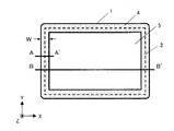
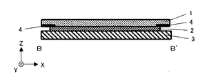
図1は本発明の実施形態である表示装置の全体構成を説明するための平面図、図2は本発明の実施形態である表示装置の全体構成を説明するための断面図であり、特に、図2は図1に示すB−B’線での断面図である。ただし、以下の説明では、表示パネル3にフロントウィンド1を固定する接着剤として透光性を有するUV硬化性樹脂(以下、UV接着剤と記す)を用いる場合について説明するが、透光性を有する熱硬化性樹脂や他の接着部材を用いる構成であってもよい。
FIG. 1 is a plan view for explaining the overall configuration of a display device according to an embodiment of the present invention, and FIG. 2 is a cross-sectional view for explaining the overall configuration of the display device according to an embodiment of the present invention. 2 is a cross-sectional view taken along line BB ′ shown in FIG. However, in the following description, a case where a UV curable resin having translucency (hereinafter referred to as a UV adhesive) is used as an adhesive for fixing the front window 1 to the
本実施形態の表示装置では、図2の断面図に示すように、表示パネル3の前面すなわち表示面側にUV接着剤(接着剤層)2でフロントウィンド1が接着され、固定されている。このとき、フロントウィンド1の裏面すなわち表示パネル3と対向する側の面(対向面)に遮光膜4が印刷で形成されている。この遮光膜4は図1に示すようにフロントウィンド1の辺縁部に沿い環状に形成され、この遮光膜4に囲まれる開口部分を介して表示パネル3からの画像が表示される。
In the display device of this embodiment, as shown in the cross-sectional view of FIG. 2, the front window 1 is bonded and fixed to the front surface of the
表示パネル3としては、例えば、一対の透明基板が液晶層を介して対向配置され、その裏面側にバックライト装置が配置される液晶表示パネルがある。液晶表示パネルでは、一方の透明基板に映像信号(ドレイン信号)が供給される複数の映像信号線(ドレイン線)と、該ドレイン線と交差するように形成され、走査信号(ゲート信号)が供給される複数の走査信号線(ゲート線)とが形成される。該ドレイン線とゲート線とが交差する近傍には薄膜トランジスタが配置され、該薄膜トランジスタのドレイン電極がドレイン線に、ゲート電極がゲート線に、ソース電極が画素電極にそれぞれ接続され、ゲート信号に同期してドレイン信号が画素電極に供給される構成となっている。また、画素電極に供給されるドレイン信号の基準となる共通信号が供給される共通電極が形成されており、画素電極とは絶縁膜を介して対向配置されて画素を形成し、該画素がドレイン線及びゲート線に沿ってマトリクス状に配置され、表示領域を形成している。さらには、他方の透明基板には画素毎に赤(R)、緑(G)、青(B)に対応したカラーフィルタが形成されており、このRGBの画素でカラー表示用の単位画素が形成され、カラー表示がなされる構成となっている。ただし、表示パネル3は前述するIPS(In-Plane Switching)方式の液晶表示パネルに限定されることはなく、他の方式の液晶表示パネルや有機EL表示パネル等の他の表示パネルであってもよい。さらには、表示パネルの観察者側すなわちフロントウィンドが配置される側の面(以下、対向面と記す)にオンセル型タッチパネルや別体で形成され表示パネルの前面にタッチパネル等が配置されている構成にも適用可能である。
As the
本願発明の表示装置においては、図1中に点線で示すように、UV接着剤2は遮光膜4の開口部を覆うように形成されると共に、その端部が遮光膜4に覆われる領域内となる。すなわち、本願発明の構成においても、表示パネル3から出力される表示画像が操作者側に出力される範囲である遮光膜4の開口領域には接着剤2が塗布されると共に、遮光膜4の内周側の辺縁領域にも接着剤2が塗布される構成となる。この構成により、本願発明の表示装置においても、接着剤2の端部等が操作者側に露出されてしまうことを防止する構成となっている。
In the display device of the present invention, as shown by the dotted line in FIG. 1, the
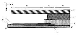
図3は本発明の実施形態である表示装置の詳細構成を説明するための拡大された断面図であり、特に、図1に示すA−A’線での断面図を示し、本実施形態の表示装置の詳細構成を説明する。ただし、図3に示す断面図は、図中に示すX軸、Y軸、Z軸から明らかなように、図2に示す断面図に対して上下方向が逆の構成となっている。すなわち、フロントウィンド1への接着剤2の塗布及びフロントウィンド1と表示パネル3とを接着する工程に対応した図面となっている。
FIG. 3 is an enlarged cross-sectional view for explaining the detailed configuration of the display apparatus according to the embodiment of the present invention. In particular, the cross-sectional view taken along the line AA ′ shown in FIG. A detailed configuration of the display device will be described. However, the cross-sectional view shown in FIG. 3 has a configuration in which the vertical direction is opposite to the cross-sectional view shown in FIG. 2, as is apparent from the X-axis, Y-axis, and Z-axis shown in the figure. That is, the drawing corresponds to the process of applying the adhesive 2 to the front window 1 and bonding the front window 1 and the
図3から明らかなように、本実施形態の表示装置では、遮光膜4は2層の遮光性を有する薄膜で形成されており、特に、フロントウィンド1に形成される第1の遮光膜41と該第1の遮光膜41の上面に形成される第2の遮光膜42とからなる。第1及び第2の遮光膜41,42は印刷技術を用いて形成されており、第1の遮光膜41よりも第2の遮光膜42のX方向幅が小さく形成されている。すなわち、第1の遮光膜41で形成される段差と第2の遮光膜42で形成される段差とがテーパー状に配置されるように、第1の遮光膜41及び第2の遮光膜42が形成されている。
As is apparent from FIG. 3, in the display device of this embodiment, the
また、本実施形態の構成では、環状の遮光膜4で囲まれる領域である開口部を覆うようにして透明印刷層5が形成されており、該透明印刷層5の端部が遮光膜4の内周側端部と重畳される構成となっている。すなわち、本実施形態の構成では、フロントウィンド1の対向面に遮光膜4のみが形成される領域(図3中に示す領域R1)と、フロントウィンド1の対向面に遮光膜4と透明印刷層5とが重畳して形成される領域(図3中に示す領域R2)と、フロントウィンド1の対向面に透明印刷層5のみが形成される領域(図3中に示す領域R3)とが形成される。ただし、本実施形態の透明印刷層5は、従来の表示装置におけるフロントウィンドと表示パネルとの間隔に相当する膜厚で形成される。この構成により、UV接着剤2の塗布量を低減させることを可能としている。なお、透明印刷層5の膜厚はこれに限定されることはなく、従来の表示装置でのフロントウィンドと表示パネルとの間隔よりも薄く形成される構成であってもよい。
In the configuration of the present embodiment, the
また、領域R2となる遮光膜4の内周側の辺縁部には、遮光膜4と透明印刷層5とが重畳して形成されている。特に、本実施形態の構成では、第1の遮光膜41を印刷で形成し、さらに該第1の遮光膜41に重畳するようにして第2の遮光膜42が印刷で形成され、遮光膜4が形成される。この後に、図3に示すように、第2の遮光膜42の内側辺縁部とこの第2の遮光膜42から露出される第1の遮光膜41の表面、及び第1の遮光膜41から露出されるフロントウィンド1の対向面側を覆うようにして、透明印刷層5が印刷により形成される。その結果、本実施形態の構成では、遮光膜4の開口部側の端部は透明印刷層5で覆われる構成となるので、遮光膜4の開口部側の端部に気泡が生じてしまうことを防止できる。
In addition, the
この後に、透明印刷層5の上層すなわち表示パネル3が接着される側の面にUV接着剤2が塗布され、表示パネル3が載置され、UV光によりUV接着剤2が硬化処理され、表示パネル3の前面にフロントウィンド1が固定される。このとき、本実施形態の構成では、透明印刷層5の上面である対向面にUV接着剤2が塗布され、該UV接着剤2が濡れ広がることとなる。この濡れ広がりは、例えば、図3に示すように、透明印刷層5の端部よりもA側に濡れ広がるUV接着剤2はその表面張力によって、UV接着剤2のA側の端面が曲面状となり、濡れ広がりが一時的に抑制されることとなる。従って、例えば、誤差を含めたUV接着剤2の塗布量及び塗布領域の最小が図3に示す範囲となるように、UV接着剤2の塗布量及び塗布領域を予め設定しておくことができる。これにより、遮光膜4の開口側の端部すなわち第1及び第2の遮光膜41,42のA’側の端部よりもフロントウィンド1の辺縁部側すなわち遮光膜4の形成領域に、UV接着剤2の端部が形成される構成とすることができる。その結果、接着剤2の端部も遮光膜4で覆われる構成となるので、操作者側から接着剤2の端部等が確認できてしまうことを防止できる。
Thereafter, the
例えば、UV接着剤2の塗布量及び塗布領域が最小値よりも多い場合、前述する図3に示す接着剤2の表面張力による範囲を超えてUV接着剤2が濡れ広がることなる。このときの図1に示すB−B’線での断面図を示したのが図4であり、図3と同様な位置での拡大された断面図となる。
For example, when the application amount and application area of the
図3に示す場合よりもUV接着剤2の塗布される量が多い場合、図4に示すように、塗布されたUV接着剤2は領域R1に濡れ広がることとなる。この場合、領域R1では遮光膜4のみが形成される構成となっているので、遮光膜4と透明印刷層5とが重畳して形成される領域R2よりもその容積が大きい構成となる。特に、本実施形態の構成では、図3及び図4に示すように、遮光膜4の膜厚よりも透明印刷層5の膜厚が大きく構成されている。その結果、領域R2及び領域R3よりも領域R1における容積が大きく形成されている。すなわち、フロントウィンド1と表示パネル3とにより形成されるZ方向すなわち厚さ方向の間隔が、領域R1>領域R3>領域R2の順となり、その容積すなわち各領域でのUV接着剤2が占める体積もこの順番となる。
When the amount of the
その結果、UV接着剤2の塗布量及び塗布領域が製造装置の誤差範囲等で大きくなった場合であっても、UV接着剤2の領域R1におけるA側方向すなわちフロントウィンド1の端部方向への濡れ広がりすなわち外周方向へのUV接着剤2の端部の移動量を他の領域R2,R3よりも抑えることが可能となる。すなわち、本実施形態の構成では、領域R1をUV接着剤2の塗布時における貯留領域として用いることが可能となるので、UV接着剤2の塗布や濡れ広がりに伴う当該UV接着剤2のはみ出しを防止することが可能となる。
As a result, even when the coating amount and the coating area of the
特に、本実施形態の構成では、透明印刷層5の膜厚によりUV接着剤2の塗布量が従来よりも大幅に低減された構成となるので、フロントウィンド1と表示パネル3との間隔が従来と同様の間隔となる領域R1での外周方向へのUV接着剤2の端部の移動量を大幅に低減させることが可能となる。また、本実施形態の構成では、透明印刷層5よりも外周側すなわち透明印刷層5が形成されない領域では、フロントウィンド1と表示パネル3との間隔は従来と同様の間隔となるので、UV接着剤2を塗布する装置も従来と同じ装置すなわち従来と同じ精度の塗布装置等を用いることができるという効果も得られる。
In particular, in the configuration of the present embodiment, the coating amount of the
ただし、本実施形態の表示装置の構成では、UV接着剤2によるフロントウィンド1と表示パネル3との接着の際に、透明印刷層5よりはみ出したUV接着剤2により透明印刷層5の端部において、透明印刷層5の形成に伴う段差部分で気泡が生じることが考えられる。しかしながら、この気泡が生じることとなる透明印刷層5の端部は、操作者側から見て遮光膜4で遮蔽される領域となるので、気泡の有無や気泡の発生に伴う表示品質の低下が防止できることとなる。
However, in the configuration of the display device according to the present embodiment, when the front window 1 and the
また、図3及び図4に示すように、本実施形態の表示装置では、フロントウィンド1の外形形状が表示パネル3の外形形状よりも大きい場合について説明したが、これに限定されることはない。例えば、フロントウィンド1の外形形状が表示パネル3の外形形状よりも小さい場合や同じ大きさであっても、前述と同様に本願発明を適用可能であり、前述と同様の効果が得られる。
Further, as shown in FIGS. 3 and 4, in the display device of the present embodiment, the case where the outer shape of the front window 1 is larger than the outer shape of the
なお、前述する説明では、図3に示す状態が最小となるように、UV接着剤2の塗布量及び塗布領域を設定する場合について説明したが、これに限定されることはない。例えば、UV接着剤2の塗布量及び塗布領域の最小の場合におけるUV接着剤2の端部の位置が、図5に示すように、遮光膜4と透明印刷層5とが重畳して形成される領域R2となる場合であってもよい。この場合には、UV接着剤2の塗布量及び塗布領域の増加に伴い、図3に示す状態を経て、図4に示す状態となるので、前述する効果に加えて、UV接着剤2の塗布時における濡れ広がりに対する余裕度を増やせるという格別の効果を得ることができる。ただし、図5に示すように、UV接着剤2の端部が遮光膜4と透明印刷層5とが重畳する部分に形成される場合は、遮光膜4の内側端部からUV接着剤2の端部に至るまでX方向の距離すなわち遮光膜4の幅方向の距離が小さくなる。このために、遮光膜4の幅方向の長さすなわち領域R2の幅が小さい場合やUV接着剤2の端部が開口部側に配置される場合、操作者が斜め方向から観察した際にUV接着剤2の端部が開口部から見えてしまうことが考えられる。従って、透明印刷層5の膜厚等を考慮して、UV接着剤2の端部位置を適宜決定する必要がある。
In the above description, the case where the application amount and application region of the
以上説明したように、本実施形態の表示装置では、フロントウィンド1の辺縁部に沿って遮光膜4が形成されると共に、該遮光膜4で囲まれる部分である開口部と該開口部に沿った部分である遮光膜4と開口部の境界部分を含む遮光膜4の内周側の辺縁部とを覆うように透明印刷層5が形成される構成となっている。さらには、遮光膜4と透明印刷層5とが形成されるフロントウィンド1と表示パネル3とが、少なくとも開口部を覆うように塗布されたUV接着剤2で接着される構成となっている。すなわち、本願発明の表示装置では、遮光膜4の上面の内で開口部近傍の上面から側面を経て開口部を覆うようにして、透明印刷層5が形成される構成となっている。その結果、UV接着剤2によるフロントウィンド1と表示パネル3との接着時における遮光膜4の内周側端部での気泡の発生、及びフロントウィンド1と表示パネル3との外周側からのUV接着剤2のはみ出しを防止できる。特に、UV接着剤2のはみ出しが生じた場合、そのはみ出したUV接着剤2を除去するための工程が必要となるが、本願発明の表示装置では、UV接着剤2のはみ出しに起因するUV接着剤2の除去が不要となるので、大幅に生産効率を向上できる。
As described above, in the display device of the present embodiment, the
また、遮光膜4が第1の遮光膜41と第2の遮光膜42との少なくとも2層の遮光膜で形成されると共に、第1の遮光膜41内周側端部と第2の遮光膜42の内周側端部とがテーパー状に段差が並設されるように、端面である内壁面がずれて形成されている。すなわち、フロントウィンド1に近い側に形成される第1の遮光膜41の内周側端部よりも第2の遮光膜42の内周側端部が開口部から離れて形成される。その結果、透明印刷層5の形成に際に、第1の遮光膜41と第2の遮光膜42との開口部に近い側の表面(露出面)から開口部にかけて形成される透明印刷層5の印刷時において、遮光膜4の内周側端部での気泡の発生も容易に防止できる。
Further, the
また、本実施形態の構成では、透明印刷層5が従来の表示装置におけるフロントウィンドと表示パネルとの間隔に相当する膜厚で形成されるので、UV接着剤2の膜厚分だけ表示装置全体の厚さが大きくなるが、表示装置全体の厚さが大きくなるので強度が向上できるという格別の効果を得ることができる。
Further, in the configuration of the present embodiment, the
さらには、フロントウィンド1と表示パネル3との間に衝撃等の緩衝部材としても機能する透明印刷層5が形成されているので、フロントウィンド1に印加された応力がUV接着剤2を介して表示パネル3に加わり、表示ムラを発生させてしまうことを防止できるという格別の効果を得ることも可能である。
Furthermore, since a
なお、本実施形態の表示装置では、第1の遮光膜41と第2の遮光膜42との2層の遮光層で遮光膜4を形成する構成としたが、1層の遮光層で遮光膜4を形成する構成であってもよい。
In the display device according to the present embodiment, the
また、本実施形態の表示装置では、遮光膜4が全ての辺において同一幅Wで形成される場合について説明したが、映像信号や走査信号を供給する駆動回路等が搭載される辺の幅が異なる場合であっても適用可能である。
In the display device according to the present embodiment, the case where the
以上、本発明者によってなされた発明を、前記発明の実施形態に基づき具体的に説明したが、本発明は、前記発明の実施形態に限定されるものではなく、その要旨を逸脱しない範囲において種々変更可能である。 As mentioned above, the invention made by the present inventor has been specifically described based on the embodiment of the invention. However, the invention is not limited to the embodiment of the invention, and various modifications can be made without departing from the scope of the invention. It can be changed.
1……フロントウィンド、2……UV接着剤、3……表示パネル、4……遮光膜
41……第1の遮光膜、42……第2の遮光膜、5……透明印刷
DESCRIPTION OF SYMBOLS 1 ... Front window, 2 ... UV adhesive, 3 ... Display panel, 4 ... Light shielding film 41 ... 1st light shielding film, 42 ... 2nd light shielding film, 5 ... Transparent printing
Claims (3)
前記フロントウィンドの辺縁部に沿って環状に形成される遮光膜と、
前記遮光膜で囲まれる開口部、及び前記遮光膜と前記開口部との境界部分に形成される段差部分、並びに前記遮光膜の対向面の内で前記段差部分の近傍領域を覆うようにして形成される透明印刷層とを有し、
前記フロントウィンドの外周部と前記段差部との間の前記遮光膜上に、前記透明印刷層の端部が形成され、
前記遮光膜と前記透明印刷層とが重畳される領域内で前記開口部に近接する領域を含み、前記透明印刷層が形成される領域と前記表示パネルとの間に少なくとも前記接着剤層が形成され、
前記接着剤層の形成時の濡れ広がりによる接着剤層が、前記表示パネル又は前記フロントウィンドの外周部と前記透明印刷層の端部との間であって、前記フロントウィンドの前記遮光層のみが形成され前記透明印刷層が形成されない領域に形成され、
前記遮光層は2層以上の遮光性を有する薄膜層からなり、前記フロントウィンドに近い側に形成される第1の薄膜層に重畳して、前記フロントウィンドから遠い側の第2の薄膜層が形成され、
前記第1の薄膜層の幅が前記第2の薄膜層の幅よりも大きく形成されることを特徴とする表示装置。 A display device having a front window for protecting a display panel, wherein the front window is fixed to a display surface side of the display panel via an adhesive layer,
A light shielding film formed in an annular shape along the edge of the front window;
Formed so as to cover an opening surrounded by the light shielding film, a stepped portion formed at a boundary portion between the light shielding film and the opening, and a region near the stepped portion of the opposing surface of the light shielding film. A transparent printed layer,
An end of the transparent printing layer is formed on the light shielding film between the outer peripheral portion of the front window and the stepped portion,
In a region where the light-shielding film and the transparent printing layer are superimposed, a region close to the opening is formed, and at least the adhesive layer is formed between the region where the transparent printing layer is formed and the display panel And
Adhesive layer by wetting of the formation of the adhesive layer, a between the end of the display panel or the transparent printing layer and the outer peripheral portion of the front window, only the light shielding layer of the front window is Formed in a region where the transparent printing layer is not formed ,
The light shielding layer is composed of two or more thin film layers having a light shielding property, and overlaps with a first thin film layer formed on a side near the front window, and a second thin film layer on a side far from the front window is provided. Formed,
Display width of the first thin film layer is characterized Rukoto is larger than the width of the second film layer.
Priority Applications (1)
| Application Number | Priority Date | Filing Date | Title |
|---|---|---|---|
| JP2012244060A JP6135902B2 (en) | 2012-11-06 | 2012-11-06 | Display device |
Applications Claiming Priority (1)
| Application Number | Priority Date | Filing Date | Title |
|---|---|---|---|
| JP2012244060A JP6135902B2 (en) | 2012-11-06 | 2012-11-06 | Display device |
Publications (3)
| Publication Number | Publication Date |
|---|---|
| JP2014092724A JP2014092724A (en) | 2014-05-19 |
| JP2014092724A5 JP2014092724A5 (en) | 2015-12-17 |
| JP6135902B2 true JP6135902B2 (en) | 2017-05-31 |
Family
ID=50936821
Family Applications (1)
| Application Number | Title | Priority Date | Filing Date |
|---|---|---|---|
| JP2012244060A Active JP6135902B2 (en) | 2012-11-06 | 2012-11-06 | Display device |
Country Status (1)
| Country | Link |
|---|---|
| JP (1) | JP6135902B2 (en) |
Cited By (1)
| Publication number | Priority date | Publication date | Assignee | Title |
|---|---|---|---|---|
| US11372273B2 (en) | 2019-04-22 | 2022-06-28 | Samsung Display Co., Ltd. | Display device and method for manufacturing the same |
Families Citing this family (1)
| Publication number | Priority date | Publication date | Assignee | Title |
|---|---|---|---|---|
| JP6456166B2 (en) * | 2015-01-30 | 2019-01-23 | 三菱電機株式会社 | Image display device and manufacturing method thereof |
Family Cites Families (12)
| Publication number | Priority date | Publication date | Assignee | Title |
|---|---|---|---|---|
| JP2005242265A (en) * | 2004-02-27 | 2005-09-08 | Mitsui Chemicals Inc | Optical filter and filter for plasma display using the same |
| JP4494446B2 (en) * | 2007-09-12 | 2010-06-30 | 株式会社 日立ディスプレイズ | Display device |
| JP2009093158A (en) * | 2007-09-21 | 2009-04-30 | Toshiba Matsushita Display Technology Co Ltd | Display element |
| JP2009251550A (en) * | 2008-04-11 | 2009-10-29 | Epson Imaging Devices Corp | Electrooptical device, input device, and electronic apparatus |
| JP5594713B2 (en) * | 2009-03-31 | 2014-09-24 | 株式会社ジャパンディスプレイ | Display device |
| JP2011007830A (en) * | 2009-06-23 | 2011-01-13 | Hitachi Displays Ltd | Display device |
| JP4992958B2 (en) * | 2009-11-30 | 2012-08-08 | カシオ計算機株式会社 | Manufacturing method of plate member assembly and manufacturing method of electronic member with transparent substrate |
| JP5509837B2 (en) * | 2009-12-21 | 2014-06-04 | カシオ計算機株式会社 | Method for joining plate-like parts and joining member |
| JP5370240B2 (en) * | 2010-03-30 | 2013-12-18 | カシオ計算機株式会社 | Display module |
| JP5535739B2 (en) * | 2010-04-13 | 2014-07-02 | 株式会社ジャパンディスプレイ | Display device |
| JP2012032652A (en) * | 2010-07-30 | 2012-02-16 | Asahi Glass Co Ltd | Front substrate for display and display device using the same |
| JP2012068278A (en) * | 2010-09-21 | 2012-04-05 | Casio Comput Co Ltd | Electronic member with protective member and method for manufacturing the same |
-
2012
- 2012-11-06 JP JP2012244060A patent/JP6135902B2/en active Active
Cited By (2)
| Publication number | Priority date | Publication date | Assignee | Title |
|---|---|---|---|---|
| US11372273B2 (en) | 2019-04-22 | 2022-06-28 | Samsung Display Co., Ltd. | Display device and method for manufacturing the same |
| US11693268B2 (en) | 2019-04-22 | 2023-07-04 | Samsung Display Co., Ltd. | Display device and method for manufacturing the same |
Also Published As
| Publication number | Publication date |
|---|---|
| JP2014092724A (en) | 2014-05-19 |
Similar Documents
| Publication | Publication Date | Title |
|---|---|---|
| US11106066B2 (en) | Electro-optical device and electronic equipment | |
| US9285625B2 (en) | Display device | |
| US10451913B2 (en) | Liquid crystal display panel | |
| JP5354523B2 (en) | Active matrix liquid crystal display device and manufacturing method thereof | |
| JP2009069321A (en) | Display device | |
| JP2014182163A (en) | Display device | |
| JP2013190808A (en) | Display element | |
| US20160334656A1 (en) | Display device | |
| KR20120090846A (en) | Liquid crystal display device | |
| US10197842B2 (en) | Liquid crystal display device | |
| JP2008176237A (en) | Liquid crystal display device | |
| US20160231774A1 (en) | Display module | |
| JP2013190715A (en) | Display device, manufacturing method, and electronic apparatus | |
| JP2011221371A5 (en) | ||
| US20190219862A1 (en) | Display device and manufacturing method thereof | |
| JP2005107165A (en) | Liquid crystal display and method for manufacturing liquid crystal display | |
| CN104460119A (en) | Display panel and method for manufacturing the same | |
| JP6135902B2 (en) | Display device | |
| WO2018225603A1 (en) | Display device with position input function | |
| JP2011247959A (en) | Display device | |
| KR102065031B1 (en) | Display apparatus having camera module | |
| JP2016038520A (en) | Display device | |
| JP2019090899A (en) | Display device | |
| US11719970B2 (en) | Display device and method of manufacturing the same, electronic equipment and method of manufacturing the same, and backlight unit | |
| KR20170079397A (en) | Display device |
Legal Events
| Date | Code | Title | Description |
|---|---|---|---|
| A521 | Request for written amendment filed |
Free format text: JAPANESE INTERMEDIATE CODE: A523 Effective date: 20151102 |
|
| A621 | Written request for application examination |
Free format text: JAPANESE INTERMEDIATE CODE: A621 Effective date: 20151102 |
|
| A977 | Report on retrieval |
Free format text: JAPANESE INTERMEDIATE CODE: A971007 Effective date: 20160915 |
|
| A131 | Notification of reasons for refusal |
Free format text: JAPANESE INTERMEDIATE CODE: A131 Effective date: 20160920 |
|
| A521 | Request for written amendment filed |
Free format text: JAPANESE INTERMEDIATE CODE: A523 Effective date: 20161118 |
|
| TRDD | Decision of grant or rejection written | ||
| A01 | Written decision to grant a patent or to grant a registration (utility model) |
Free format text: JAPANESE INTERMEDIATE CODE: A01 Effective date: 20170404 |
|
| A61 | First payment of annual fees (during grant procedure) |
Free format text: JAPANESE INTERMEDIATE CODE: A61 Effective date: 20170412 |
|
| R150 | Certificate of patent or registration of utility model |
Ref document number: 6135902 Country of ref document: JP Free format text: JAPANESE INTERMEDIATE CODE: R150 |
|
| R250 | Receipt of annual fees |
Free format text: JAPANESE INTERMEDIATE CODE: R250 |
|
| R250 | Receipt of annual fees |
Free format text: JAPANESE INTERMEDIATE CODE: R250 |
|
| R250 | Receipt of annual fees |
Free format text: JAPANESE INTERMEDIATE CODE: R250 |
|
| R250 | Receipt of annual fees |
Free format text: JAPANESE INTERMEDIATE CODE: R250 |
|
| R250 | Receipt of annual fees |
Free format text: JAPANESE INTERMEDIATE CODE: R250 |