KR101935552B1 - flexible display panel and the display apparatus comprising the flexible display panel - Google Patents
flexible display panel and the display apparatus comprising the flexible display panel Download PDFInfo
- Publication number
- KR101935552B1 KR101935552B1 KR1020120069471A KR20120069471A KR101935552B1 KR 101935552 B1 KR101935552 B1 KR 101935552B1 KR 1020120069471 A KR1020120069471 A KR 1020120069471A KR 20120069471 A KR20120069471 A KR 20120069471A KR 101935552 B1 KR101935552 B1 KR 101935552B1
- Authority
- KR
- South Korea
- Prior art keywords
- region
- display
- flexible
- display area
- protective film
- Prior art date
- Legal status (The legal status is an assumption and is not a legal conclusion. Google has not performed a legal analysis and makes no representation as to the accuracy of the status listed.)
- Active
Links
Images


Classifications
-
- H—ELECTRICITY
- H05—ELECTRIC TECHNIQUES NOT OTHERWISE PROVIDED FOR
- H05B—ELECTRIC HEATING; ELECTRIC LIGHT SOURCES NOT OTHERWISE PROVIDED FOR; CIRCUIT ARRANGEMENTS FOR ELECTRIC LIGHT SOURCES, IN GENERAL
- H05B33/00—Electroluminescent light sources
- H05B33/12—Light sources with substantially two-dimensional [2D] radiating surfaces
- H05B33/22—Light sources with substantially two-dimensional [2D] radiating surfaces characterised by the chemical or physical composition or the arrangement of auxiliary dielectric or reflective layers
-
- G—PHYSICS
- G09—EDUCATION; CRYPTOGRAPHY; DISPLAY; ADVERTISING; SEALS
- G09F—DISPLAYING; ADVERTISING; SIGNS; LABELS OR NAME-PLATES; SEALS
- G09F9/00—Indicating arrangements for variable information in which the information is built-up on a support by selection or combination of individual elements
-
- G—PHYSICS
- G06—COMPUTING OR CALCULATING; COUNTING
- G06F—ELECTRIC DIGITAL DATA PROCESSING
- G06F1/00—Details not covered by groups G06F3/00 - G06F13/00 and G06F21/00
- G06F1/16—Constructional details or arrangements
- G06F1/1601—Constructional details related to the housing of computer displays, e.g. of CRT monitors, of flat displays
-
- G—PHYSICS
- G06—COMPUTING OR CALCULATING; COUNTING
- G06F—ELECTRIC DIGITAL DATA PROCESSING
- G06F1/00—Details not covered by groups G06F3/00 - G06F13/00 and G06F21/00
- G06F1/16—Constructional details or arrangements
- G06F1/1613—Constructional details or arrangements for portable computers
- G06F1/1633—Constructional details or arrangements of portable computers not specific to the type of enclosures covered by groups G06F1/1615 - G06F1/1626
- G06F1/1637—Details related to the display arrangement, including those related to the mounting of the display in the housing
- G06F1/1643—Details related to the display arrangement, including those related to the mounting of the display in the housing the display being associated to a digitizer, e.g. laptops that can be used as penpads
-
- G—PHYSICS
- G06—COMPUTING OR CALCULATING; COUNTING
- G06F—ELECTRIC DIGITAL DATA PROCESSING
- G06F1/00—Details not covered by groups G06F3/00 - G06F13/00 and G06F21/00
- G06F1/16—Constructional details or arrangements
- G06F1/1613—Constructional details or arrangements for portable computers
- G06F1/1633—Constructional details or arrangements of portable computers not specific to the type of enclosures covered by groups G06F1/1615 - G06F1/1626
- G06F1/1637—Details related to the display arrangement, including those related to the mounting of the display in the housing
- G06F1/1652—Details related to the display arrangement, including those related to the mounting of the display in the housing the display being flexible, e.g. mimicking a sheet of paper, or rollable
-
- G—PHYSICS
- G06—COMPUTING OR CALCULATING; COUNTING
- G06F—ELECTRIC DIGITAL DATA PROCESSING
- G06F3/00—Input arrangements for transferring data to be processed into a form capable of being handled by the computer; Output arrangements for transferring data from processing unit to output unit, e.g. interface arrangements
- G06F3/01—Input arrangements or combined input and output arrangements for interaction between user and computer
- G06F3/03—Arrangements for converting the position or the displacement of a member into a coded form
- G06F3/041—Digitisers, e.g. for touch screens or touch pads, characterised by the transducing means
- G06F3/0412—Digitisers structurally integrated in a display
-
- H—ELECTRICITY
- H05—ELECTRIC TECHNIQUES NOT OTHERWISE PROVIDED FOR
- H05B—ELECTRIC HEATING; ELECTRIC LIGHT SOURCES NOT OTHERWISE PROVIDED FOR; CIRCUIT ARRANGEMENTS FOR ELECTRIC LIGHT SOURCES, IN GENERAL
- H05B33/00—Electroluminescent light sources
- H05B33/02—Details
- H05B33/04—Sealing arrangements, e.g. against humidity
-
- H—ELECTRICITY
- H10—SEMICONDUCTOR DEVICES; ELECTRIC SOLID-STATE DEVICES NOT OTHERWISE PROVIDED FOR
- H10K—ORGANIC ELECTRIC SOLID-STATE DEVICES
- H10K50/00—Organic light-emitting devices
- H10K50/80—Constructional details
- H10K50/84—Passivation; Containers; Encapsulations
- H10K50/844—Encapsulations
-
- H—ELECTRICITY
- H10—SEMICONDUCTOR DEVICES; ELECTRIC SOLID-STATE DEVICES NOT OTHERWISE PROVIDED FOR
- H10K—ORGANIC ELECTRIC SOLID-STATE DEVICES
- H10K59/00—Integrated devices, or assemblies of multiple devices, comprising at least one organic light-emitting element covered by group H10K50/00
- H10K59/10—OLED displays
- H10K59/12—Active-matrix OLED [AMOLED] displays
- H10K59/131—Interconnections, e.g. wiring lines or terminals
-
- H—ELECTRICITY
- H10—SEMICONDUCTOR DEVICES; ELECTRIC SOLID-STATE DEVICES NOT OTHERWISE PROVIDED FOR
- H10K—ORGANIC ELECTRIC SOLID-STATE DEVICES
- H10K59/00—Integrated devices, or assemblies of multiple devices, comprising at least one organic light-emitting element covered by group H10K50/00
- H10K59/80—Constructional details
- H10K59/87—Passivation; Containers; Encapsulations
- H10K59/873—Encapsulations
-
- H—ELECTRICITY
- H10—SEMICONDUCTOR DEVICES; ELECTRIC SOLID-STATE DEVICES NOT OTHERWISE PROVIDED FOR
- H10K—ORGANIC ELECTRIC SOLID-STATE DEVICES
- H10K77/00—Constructional details of devices covered by this subclass and not covered by groups H10K10/80, H10K30/80, H10K50/80 or H10K59/80
- H10K77/10—Substrates, e.g. flexible substrates
- H10K77/111—Flexible substrates
-
- G—PHYSICS
- G02—OPTICS
- G02F—OPTICAL DEVICES OR ARRANGEMENTS FOR THE CONTROL OF LIGHT BY MODIFICATION OF THE OPTICAL PROPERTIES OF THE MEDIA OF THE ELEMENTS INVOLVED THEREIN; NON-LINEAR OPTICS; FREQUENCY-CHANGING OF LIGHT; OPTICAL LOGIC ELEMENTS; OPTICAL ANALOGUE/DIGITAL CONVERTERS
- G02F1/00—Devices or arrangements for the control of the intensity, colour, phase, polarisation or direction of light arriving from an independent light source, e.g. switching, gating or modulating; Non-linear optics
- G02F1/01—Devices or arrangements for the control of the intensity, colour, phase, polarisation or direction of light arriving from an independent light source, e.g. switching, gating or modulating; Non-linear optics for the control of the intensity, phase, polarisation or colour
- G02F1/13—Devices or arrangements for the control of the intensity, colour, phase, polarisation or direction of light arriving from an independent light source, e.g. switching, gating or modulating; Non-linear optics for the control of the intensity, phase, polarisation or colour based on liquid crystals, e.g. single liquid crystal display cells
- G02F1/133—Constructional arrangements; Operation of liquid crystal cells; Circuit arrangements
- G02F1/1333—Constructional arrangements; Manufacturing methods
- G02F1/133308—Support structures for LCD panels, e.g. frames or bezels
-
- G—PHYSICS
- G06—COMPUTING OR CALCULATING; COUNTING
- G06F—ELECTRIC DIGITAL DATA PROCESSING
- G06F2203/00—Indexing scheme relating to G06F3/00 - G06F3/048
- G06F2203/041—Indexing scheme relating to G06F3/041 - G06F3/045
- G06F2203/04102—Flexible digitiser, i.e. constructional details for allowing the whole digitising part of a device to be flexed or rolled like a sheet of paper
-
- H—ELECTRICITY
- H10—SEMICONDUCTOR DEVICES; ELECTRIC SOLID-STATE DEVICES NOT OTHERWISE PROVIDED FOR
- H10K—ORGANIC ELECTRIC SOLID-STATE DEVICES
- H10K2102/00—Constructional details relating to the organic devices covered by this subclass
- H10K2102/301—Details of OLEDs
- H10K2102/311—Flexible OLED
-
- Y—GENERAL TAGGING OF NEW TECHNOLOGICAL DEVELOPMENTS; GENERAL TAGGING OF CROSS-SECTIONAL TECHNOLOGIES SPANNING OVER SEVERAL SECTIONS OF THE IPC; TECHNICAL SUBJECTS COVERED BY FORMER USPC CROSS-REFERENCE ART COLLECTIONS [XRACs] AND DIGESTS
- Y02—TECHNOLOGIES OR APPLICATIONS FOR MITIGATION OR ADAPTATION AGAINST CLIMATE CHANGE
- Y02E—REDUCTION OF GREENHOUSE GAS [GHG] EMISSIONS, RELATED TO ENERGY GENERATION, TRANSMISSION OR DISTRIBUTION
- Y02E10/00—Energy generation through renewable energy sources
- Y02E10/50—Photovoltaic [PV] energy
- Y02E10/549—Organic PV cells
Landscapes
- Engineering & Computer Science (AREA)
- Theoretical Computer Science (AREA)
- General Engineering & Computer Science (AREA)
- Computer Hardware Design (AREA)
- Physics & Mathematics (AREA)
- General Physics & Mathematics (AREA)
- Human Computer Interaction (AREA)
- Microelectronics & Electronic Packaging (AREA)
- Optics & Photonics (AREA)
- Devices For Indicating Variable Information By Combining Individual Elements (AREA)
- Electroluminescent Light Sources (AREA)
Abstract
본 발명의 일 측면에 의하면. 표시 영역을 포함하고 제1 면에 형성된 제1 영역과, 비표시 영역을 포함하고 상기 제1 면에 대하여 접힌 제2 면에 형성된 제2 영역을 구비하는 가요성 패널; 적어도 상기 표시 영역을 봉지하도록 상기 가요성 패널 상에 배치된 가요성 봉지 부재; 및 상기 가요성 패널 및 상기 가요성 봉지 부재의 양측에 각각 배치된 제1 보호필름 및 제2 보호필름;을 포함하는 가요성 표시 패널을 제공한다. According to one aspect of the invention. A flexible panel having a first area including a display area and formed on a first surface, and a second area including a non-display area and formed on a second surface folded against the first surface; A flexible sealing member disposed on the flexible panel to seal at least the display area; And a first protective film and a second protective film disposed on both sides of the flexible panel and the flexible sealing member, respectively.
Description
본 발명은 가요성 표시 패널 및 상기 가요성 표시 패널을 포함하는 표시 장치에 관한 것이다.The present invention relates to a flexible display panel and a display device including the flexible display panel.
표시 장치란 영상 신호를 표시하는 장치를 의미한다. 이러한 표시 장치는 텔레비전, 컴퓨터 모니터, PDA, 및 최근 폭발적으로 수요가 증가한 스마트 기기 등을 포함하여, 외부에서 입력되는 영상 신호를 표시하는 모든 장치를 포함하는 개념이다.The display device means a device for displaying a video signal. Such a display device is a concept that includes all devices that display video signals input from the outside, including televisions, computer monitors, PDAs, and smart devices that have recently increased in explosion demand.
상기 표시 장치에 유기 발광 표시 패널, 액정 표시 패널, 플라즈마 디스플레이 패널 등과 같은 고화질의 평판형 표시 모듈이 사용되고 있다. A high-definition flat panel display module such as an organic light emitting display panel, a liquid crystal display panel, a plasma display panel, or the like is used for the display device.
상기 평판형 표시 모듈은 영상을 표시하는 표시 영역과, 상기 표시 영역에 영상 신호를 공급하기 위한 각종 회로와 배선을 포함하는 비표시 영역이, 표시 영역의 외곽에 비표시 영역과 동일 평면 상에 배치된다. The flat panel display module includes a display area for displaying an image, a non-display area including various circuits and wiring for supplying a video signal to the display area, arranged on the same plane as the non- do.
최근, 표시 장치에 대한 고화질 및 다양한 애플리케이션의 요구가 증대되면서, 평판형 표시 모듈의 비표시 영역에 배치되는 회로 및 배선의 수가 증가하고 있다. 이로 인하여 비표시 영역의 면적이 증가하여 사용자가 인식하는 표시 영역의 비율이 줄어드는 문제가 있다.2. Description of the Related Art In recent years, the number of circuits and wirings disposed in a non-display area of a flat panel display module has increased as the demand for high image quality and various applications for a display device has increased. As a result, the area of the non-display area increases and the ratio of the display area recognized by the user decreases.
본 발명은 상기와 같은 문제 및 그 밖의 문제를 해결하기 위한 것으로, 사용자에게 인식되는 비표시 영역을 현저히 줄이고, 벤딩 시 휨 스트레스에 의한 배선의 크랙을 방지할 수 있는 가요성 표시 패널 및 이를 포함한 표시 장치를 제공하는 것을 목적으로 한다.SUMMARY OF THE INVENTION The present invention has been made to solve the above-mentioned problems and other problems, and it is an object of the present invention to provide a flexible display panel capable of remarkably reducing a non-display area recognized by a user and preventing cracking of wiring due to bending stress during bending, And an object of the present invention is to provide a device.
본 발명의 일 측면에 의하면, 표시 영역을 포함하고 제1 면에 형성된 제1 영역과, 비표시 영역을 포함하고 상기 제1 면에 대하여 접힌 제2 면에 형성된 제2 영역을 구비하는 가요성 패널; 적어도 상기 표시 영역을 봉지하도록 상기 가요성 패널 상에 배치된 가요성 봉지 부재; 및 상기 가요성 패널 및 상기 가요성 봉지 부재의 양측에 각각 배치된 제1 보호필름 및 제2 보호필름;을 포함하는 가요성 표시 패널을 제공한다. According to an aspect of the present invention, there is provided a display device including: a flexible panel including a display area and including a first area formed on a first surface and a second area formed on a second surface including a non- ; A flexible sealing member disposed on the flexible panel to seal at least the display area; And a first protective film and a second protective film disposed on both sides of the flexible panel and the flexible sealing member, respectively.
상기 제1 보호필름 및 상기 제2 보호필름은 상기 표시 영역 및 상기 비표시 영역을 모두 커버하도록 배치될 수 있다. The first protective film and the second protective film may be arranged to cover both the display area and the non-display area.
상기 제1 보호필름 및 상기 제2 보호필름은 상기 표시 영역 및 상기 비표시 영역을 모두 커버하도록 배치될 수 있다. The first protective film and the second protective film may be arranged to cover both the display area and the non-display area.
상기 표시 영역은 상기 제1 평면이 향하는 제1 방향에서 보이고, 상기 비표시 영역은 상기 제1 방향에서 보이지 않을 수 있다. The display region may be seen in a first direction toward the first plane, and the non-display region may be invisible in the first direction.
상기 가요성 표시 패널이 접히지 않은 경우, 상기 제1 면이 향하는 제1 방향에서 보이는 표시 영역에 대한 비표시 영역의 면적비는, 상기 가요성 표시 패널이 접힌 경우, 상기 제1 면이 향하는 상기 제1 방향에서 보이는 표시 영역에 대한 비표시 영역의 면적비보다 작은 가요성 표시 패널.Wherein when the flexible display panel is not folded, the area ratio of the non-display area with respect to the display area in the first direction in which the first surface faces is smaller than the area ratio of the non- The area ratio of the non-display area with respect to the display area viewed in the direction of the display area.
상기 제1 영역과 제2 영역 사이에, 미리 결정된 곡률 반경을 갖는 곡면이 형성된 경계 영역이 구비될 수 있다. A boundary region in which a curved surface having a predetermined radius of curvature is formed may be provided between the first region and the second region.
상기 미리 결정된 곡률 반경은 일정한 값을 가질 수 있다. The predetermined radius of curvature may have a constant value.
상기 곡률 반경은 0.01mm 이상 10mm 이하일 수 있다. The radius of curvature may be 0.01 mm or more and 10 mm or less.
상기 경계 영역의 곡면은 아크(arc) 형상일 수 있다. The curved surface of the boundary region may be arc-shaped.
상기 경계 영역에, 상기 제1 영역 상의 표시 영역이 연장되어 위치할 수 있다. The display area on the first area may be extended and positioned in the boundary area.
상기 경계 영역에, 상기 제2 영역 상의 비표시 영역이 연장되어 위치할 수 있다. And the non-display region on the second region may be extended and positioned in the boundary region.
상기 경계 영역에, 상기 제1 영역 상의 표시 영역 및 상기 제2 영역 상의 비표시 영역이 각각 연장되어 위치할 수 있다. The display region on the first region and the non-display region on the second region may be respectively extended and positioned in the boundary region.
상기 가요성 기판은, 상기 제2 영역의 단부에서 연장되고 상기 제1 영역에 평행한 방향으로 연장된 제3 영역을 더 포함할 수 있다. The flexible substrate may further include a third region extending from an end of the second region and extending in a direction parallel to the first region.
상기 비표시 영역은 상기 제2 영역으로부터 상기 제3 영역으로 연장될 수 있다. The non-display area may extend from the second area to the third area.
상기 제3 영역에 패드부가 위치할 수 있다. The pad portion may be located in the third region.
상기 가요성 기판과, 상기 제1 영역과 제2 영역 사이에 베리어막이 더 포함될 수 있다. The flexible substrate may further include a barrier film between the first region and the second region.
상기 제1 보호필름 및 상기 제2 보호필름은 대칭적으로 배치될 수 있다. The first protective film and the second protective film may be arranged symmetrically.
상기 제1 보호필름 및 상기 제2 보호필름 중 적어도 하나는 편광필름일 수 있다. At least one of the first protective film and the second protective film may be a polarizing film.
상기 제1 보호필름은 상기 가요성 패널의 단부를 커버하고, 상기 제2 보호필름은 상기 봉지 부재의 단부를 커버할 수 있다. The first protective film covers the end portion of the flexible panel, and the second protective film covers the end portion of the sealing member.
상기 봉지 부재는 무기 절연막 및 유기 절연막 중 적어도 하나의 절연막을 포함할 수 있다. The sealing member may include at least one of an inorganic insulating film and an organic insulating film.
상기 가요성 기판 및 상기 봉지 부재 중, 상기 표시 영역의 이미지가 표시되는 적어도 어느 일측에 터치 패널이 더 구비될 수 있다. The touch panel may be further provided on at least one side of the flexible substrate and the sealing member on which an image of the display region is displayed.
상기 터치 패널은, 상기 가요성 표시 패널의 형상에 대응되도록 접힐 수 있는 가요성 필름을 포함할 수 있다. The touch panel may include a flexible film foldable to correspond to the shape of the flexible display panel.
상기 터치 패널은, 상기 가요성 필름 상에 위치하고 상기 표시 영역에 대응하는 터치 영역, 및 상기 터치 영역 외곽에 위치하는 배선 영역을 포함할 수 있다.The touch panel may include a touch region located on the flexible film and corresponding to the display region, and a wiring region located outside the touch region.
본 발명의 다른 측면에 의하면, 표시 영역을 포함하고 제1 면에 배치된 제1 영역과, 비표시 영역을 포함하고 상기 제1 면에 대하여 접힌 제2 면에 배치된 제2 영역을 구비하는 가요성 패널; 적어도 상기 표시 영역을 봉지하도록 상기 가요성 패널 상에 배치된 가용성 봉지 부재; 상기 가요성 패널 및 상기 가요성 봉지 부재의 양측에 각각 배치되고, 상기 표시 영역 및 비표시 영역을 커버하도록 배치된 제1 보호필름 및 제2 보호필름; 적어도 상기 표시 영역을 봉지하도록 상기 가요성 패널 상에 배치된 가요성 봉지 부재; 및 상기 가요성 표시 패널의 형상을 유지하는 지지 수단;을 포함하는 표시 장치를 제공할 수 있다. According to another aspect of the present invention, there is provided a display device including: a first area including a display area and disposed on a first surface; and a second area including a non-display area and disposed on a second surface folded with respect to the first surface Sex panel; A flexible sealing member disposed on the flexible panel to seal at least the display area; A first protective film and a second protective film which are disposed on both sides of the flexible panel and the flexible sealing member and arranged to cover the display area and the non-display area; A flexible sealing member disposed on the flexible panel to seal at least the display area; And a supporting means for holding the shape of the flexible display panel.
상기와 같은 본 발명의 실시예들에 따른 표시 장치에 따르면 다음과 같은 효과를 제공할 수 있다.According to the display device according to the embodiments of the present invention as described above, the following effects can be provided.
첫째, 비표시 영역을 표시 영역과 반대 방향으로 벤딩함으로써 사용자에게 인식되는 비표시 영역의 경계를 현저히 줄일 수 있다. First, by bending the non-display area in the direction opposite to the display area, the boundary of the non-display area recognized by the user can be remarkably reduced.
둘째, 가요성 표시 패널의 상하부에 금속층이 형성된 영역을 모두 커버하는 보호필름을 배치함으로써, 벤딩 시 휨 스트레스에 의한 배선의 크랙을 방지할 수 있다. Second, by disposing a protective film covering all the regions where the metal layer is formed on the upper and lower portions of the flexible display panel, it is possible to prevent the wiring from being cracked due to bending stress during bending.
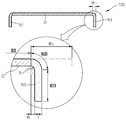
도 1은 본 발명의 제1 실시예에 따른 가요성 표시 패널(100)을 개략적으로 도시한 사시도이다.
도 2는 도 1의 Ⅱ-Ⅱ를 따라 취한 단면도이다.
도 3은 제1 실시예의 비교예에 따른 평판 표시 패널(10)을 개략적으로 도시한 사시도이다.
도 4는 도 3의 Ⅳ-Ⅳ를 따라 취한 단면도이다.
도 5는 도 1의 비표시 영역이 접히기 전 가요성 표시 패널(100-B)의 일 예를 개략적으로 도시한 평면도이다.
도 6은 도 5의 평판 표시 패널의 벤딩 전후의 상태를 개략적으로 도시한 단면도이다.
도 7은 5의 표시 영역의 일 예를 도시한 단면도이다.
도 8은 제1 실시예의 비교예에 따른 평판 표시 패널의 벤딩전후의 상태를 개략적으로 도시한 단면도이다.
도 9는 표시 영역과 비표시 영역의 접힌 부분의 내측 곡률 반경과 사용자에게 인식되는 비표시 영역의 폭의 관계를 도시한 도면이다.
도 10 및 도 11은 경계 영역(B)의 예를 도시한 단면도이다.
도 12은 본 발명의 제2 실시예에 따른 가요성 표시 패널(200)을 개략적으로 도시한 사시도이다.
도 13는 도 12의 ⅩⅢ-ⅩⅢ를 따라 취한 단면도이다.
도 14는 도 12의 비표시 영역이 접히기 전 상태의 가요성 표시 패널(200-B)의 일 예를 개략적으로 도시한 평면도이다.
도 15는 도 12의 제2 실시예의 변형예에 따른 가요성 표시 패널(200-1)을 개략적으로 도시한 사시도이다.
도 16는 도 14의 ⅩⅥ-ⅩⅥ를 따라 취한 단면도이다.
도 17은 본 발명의 제3 실시예에 따른 가요성 표시 패널(300)을 개략적으로 도시한 사시도이다.
도 18은 도 17의 ⅩⅧ-ⅩⅧ를 따라 취한 단면도이다.
도 19는 도 17의 비표시 영역이 접히기 전 상태의 가요성 표시 패널(300-B)의 일 예를 개략적으로 도시한 평면도이다.
도 20은 도 17의 제3 실시예의 변형예에 따른 가요성 표시 패널(300-1)을 개략적으로 도시한 사시도이다.
도 21은 도 20의 ⅩⅩⅠ-ⅩⅩⅠ를 따라 취한 단면도이다.
도 22는 본 발명의 제4 실시예에 따른 터치패널 일체형 가요성 표시 패널(400)에 대한 단면도이다.
도 23은 도 22의 터치패널 일체형 가요성 표시 패널(400)의 비표시 영역이 접히기 전의 터치패널 일체형 가요성 표시 패널(400-B)의 대한 단면도이다.
도 24는 도 23의 분리 사시도이다.
도 25 내지 27은 가요성 표시 패널이 지지 수단에 결합된 예들을 개략적으로 도시한 단면도들이다.1 is a perspective view schematically showing a
2 is a cross-sectional view taken along line II-II in FIG.
3 is a perspective view schematically showing a flat
4 is a cross-sectional view taken along line IV-IV in FIG.
Fig. 5 is a plan view schematically showing an example of the flexible display panel 100-B before the non-display area of Fig. 1 is folded.
6 is a cross-sectional view schematically showing a state before and after bending of the flat panel display panel of Fig.
7 is a cross-sectional view showing an example of a display region of 5;
8 is a cross-sectional view schematically showing the state before and after bending of the flat panel display panel according to the comparative example of the first embodiment.
9 is a diagram showing the relationship between the inner radius of curvature of the folded part of the display area and the non-display area and the width of the non-display area recognized by the user.
10 and 11 are cross-sectional views showing examples of the boundary region (B).
12 is a perspective view schematically showing a
13 is a cross-sectional view taken along the line XIII-XIII in Fig.
Fig. 14 is a plan view schematically showing an example of the flexible display panel 200-B in a state before the non-display area of Fig. 12 is folded.
15 is a perspective view schematically showing a flexible display panel 200-1 according to a modification of the second embodiment of Fig.
Fig. 16 is a cross-sectional view taken along the line XVI-XVI in Fig. 14. Fig.
17 is a perspective view schematically showing a
18 is a cross-sectional view taken along the line XVIII-XVIII in Fig.
Fig. 19 is a plan view schematically showing an example of the flexible display panel 300-B in the state before the non-display area of Fig. 17 is folded.
20 is a perspective view schematically showing a flexible display panel 300-1 according to a modification of the third embodiment shown in Fig.
21 is a cross-sectional view taken along XXI-XXI of Fig.
22 is a sectional view of a touch panel integrated type
23 is a sectional view of the touch panel integrated type flexible display panel 400-B before the non-display area of the touch panel integrated
Fig. 24 is an exploded perspective view of Fig. 23. Fig.
25 to 27 are sectional views schematically showing examples in which the flexible display panel is coupled to the support means.
이하, 첨부된 도면들을 참조하여 본 발명의 바람직한 실시예들을 상세히 설명한다.Hereinafter, preferred embodiments of the present invention will be described in detail with reference to the accompanying drawings.
도 1은 본 발명의 제1 실시예에 따른 가요성 표시 패널(100)을 개략적으로 도시한 사시도, 도 2는 도 1의 Ⅱ-Ⅱ를 따라 취한 단면도이다.FIG. 1 is a perspective view schematically showing a
도 1 및 도 2를 참조하면, 가요성 표시 패널(100)은 제1 면(x-y면)에 배치된 표시 영역(D)과, 상기 제1 면(x-y)에 대하여 접힌 제2 면(y-z면)에 배치되고 상기 표시 영역(D) 외곽에 배치된 비표시 영역(N1, N2, N3, N4)을 구비한다. 비표시 영역(N1, N2, N3, N4) 중 표시 영역(D)에 대하여 좌우로 서로 마주보는 비표시 영역(N1, N3)이 표시 영역(D)이 향하는 방향(z)과 반대 방향(-z)을 향하도록 접혀있다. 1 and 2, the
비표시 영역(N1, N3)이 표시 영역(D)이 향하는 방향(z)과 반대 방향(-z)으로 접혀 있기 때문에, 사용자가 표시 영역(D)의 정면(z)에서 가요성 표시 패널(100)을 바라볼 때, 사용자에게는 비표시 영역(N1, N3)의 접혀 있는 폭(W1)이 표시 영역(D)의 좌우를 둘러싸는 경계(border)로 인식된다. Since the non-display areas N1 and N3 are folded in the direction z opposite to the direction z of the display area D, The folded width W 1 of the non-display areas N1 and N3 is recognized as a border surrounding the left and right sides of the display area D to the user.
도 2를 참조하면, 비표시 영역(N1, N3)이 접히기 전의 원래 폭(W0)에 비하여 접힌 상태의 폭(W1)이 훨씬 줄어들기 때문에, 사용자에게는 비표시 영역(N1, N3)에 의한 표시 영역(D)의 경계가 훨씬 감소된 것으로 인식된다. 만약, 비표시 영역(N1, N3)을 접기 전과 접은 후의 표시 영역(D)의 면적이 그대로라면, 사용자에게 인식되는 표시 영역(D)에 대한 비표시 영역(N1, N3)의 면적비가 줄어들어, 상대적으로 표시 영역(D)이 확대된 것과 같은 효과를 줄 수 있다. 한편, 줄어든 비표시 영역(N1, N3)의 폭(W0-W1)만큼 표시 영역(D)의 폭을 확대할 수 있기 때문에, 본 실시예에 따른 가요성 표시 패널(100)이 동일 규격의 표시 장치에 적용된다면, 타 표시 패널에 비하여 확대된 영상 화면을 구현할 수 있다.2, since the width W 1 in the folded state is much smaller than the original width W 0 before the
한편, 비표시 영역(N1, N3)의 접힌 폭(W1)은 표시 영역(D)과 비표시 영역(N1, N3)의 접힌 부분의 내측 곡률 반경(R)과 가요성 표시 패널(100)의 두께(T)의 합에 의해 결정될 수 있다. 후술하겠지만 표시 영역(D)과 비표시 영역(N1, N3)의 접힌 부분의 내측 곡률 반경(R)과 가요성 표시 패널(100)의 두께(T)는 상당히 줄일 수 있기 때문에, 사용자에게는 비표시 영역(N1, N3)에 의한 표시 영역(D)의 경계가 거의 없는(borderless) 것으로 인식될 수 있다.On the other hand, the folded width of the non-display area (N1, N3) (W 1) is the display area (D) and the non-display area (N1, N3), the inner radius of curvature (R) and the flexible display panel of the folds of the 100 Of the thickness T of the substrate W. The inner radius of curvature R of the folded portion of the display area D and the non-display areas N1 and N3 and the thickness T of the
도 3은 제1 실시예의 비교예로서, 비표시 영역(N1, N2, N3, N4)을 접지 않은 평판 표시 패널(10)을 개략적으로 도시한 사시도이고, 도 4는 도 3의 Ⅳ-Ⅳ를 따라 취한 단면도이다. 3 is a perspective view schematically showing a flat
도 3 및 도 4를 참조하면, 비표시 영역(N1, N2, N3, N4)을 접지 않은 평판 표시 패널(10)은 표시 영역(D)과, 상기 표시 영역(D) 외곽에 배치된 비표시 영역(N1, N2, N3, N4)을 구비한다. 3 and 4, the flat
비표시 영역(N1, N3)이 접혀 있지 않기 때문에, 사용자가 표시 영역(D)의 정면(z)에서 평판 표시 패널(10)을 바라볼 때, 사용자에게는 비표시 영역(N1, N3) 원래의 폭(W0)이 표시 영역(D)의 좌우를 둘러싸는 경계(border)로 인식된다. 따라서, 전술한 본 발명의 제1 실시예에 따른 가요성 패널 패널(100)에 비하여 비표시 영역(N1, N2)에 의한 표시 영역(D)의 경계가 두껍게 인식된다.When the user looks at the flat
만약, 전술한 본 발명의 제1 실시예에 따른 가요성 표시 패널(100)과 본 비교예의 평판 표시 패널(10)의 표시 영역(D) 및 비표시 영역(N1, N2, N2, N3)의 면적이 각각 동일하다면, 본 발명의 제1 실시예에 따른 가요성 표시 패널(100)은 비교예의 평판 표시 패널(10)보다, 사용자에게 인식되는 표시 영역(D)에 대한 비표시 영역(N1, N3)의 면적비가 줄어들어, 표시 화면이 확대된 것과 같은 효과를 줄 수 있다.If the display area D and the non-display areas N1, N2, N2, and N3 of the
한편, 비교예에 따른 평판 표시 패널(10)의 경우, 비표시 영역(N1, N3)의 면적을 줄이기 위해서는 비표시 영역(N1, N3)에 배치되는 각종 회로, 배선부의 수를 줄이거나 그 선폭을 줄여야 한다. 그러나, 표시 장치에 대한 고화질 및 다양한 애플리케이션의 요구가 증가하고 있기 때문에, 회로나 배선부의 수를 줄이는 데 한계가 있다. 또한, 선폭을 줄이는데 공정 상의 어려움이 존재한다. 그러나, 본 실시예에 따른 가요성 표시 패널(100)은 비표시 영역(N1, N3)에 배치된 회로나 배선의 수를 줄이거나 선폭을 줄이지 않고 사용자에게 인식되는 비표시 영역의 면적을 줄일 수 있다. In the case of the flat
도 5는 도 1의 비표시 영역(N1, N3)이 접히기 전 가요성 표시 패널(100-B)의 일 예를 개략적으로 도시한 평면도이고, 도 6은 도 5의 평판 표시 패널의 벤딩 전후의 상태를 개략적으로 도시한 단면도이고, 도 7은 5의표시 영역(D)의 일 예를 도시한 단면도이다. FIG. 5 is a plan view schematically showing an example of the flexible display panel 100-B before the non-display areas N1 and N3 of FIG. 1 are folded, FIG. 6 is a cross- FIG. 7 is a cross-sectional view showing an example of the display area D of 5. FIG.
도 5 내지 7을 참조하면, 비표시 영역(N1, N3)이 접히기 전 가요성 표시 패널(100-B)은 가요성 기판(111), 가요성 기판(111) 상에 배치된 베리어막(112), 베리어막(112) 상에 배치된 표시 영역(D) 및 비표시 영역(N1, N2, N3, N4), 가요성 봉지 부재(113), 가요성 기판(111)의 일측에 배치된 제1 보호필름(114), 및 상기 가요성 봉지 부재(113)의 일측에 배치된 제2 보호필름(115)을 구비한다. 5 to 7, before the non-display areas N1 and N3 are folded, the flexible display panel 100-B includes a
가요성 기판(111)은 폴리에틸렌에테르프탈레이트, 폴리에틸렌나프탈레이트, 폴리카보네이트, 폴리아릴레이트, 폴리에테르이미드, 폴리에테르술폰, 및 폴리이미드 등과 같이 내열성 및 내구성이 우수한 플라스틱을 소재로 만들어 질 수 있다. 그러나 본 발명은 이에 한정되지 않으며, 가요성 있는 다양한 소재가 사용될 수 있다. The
가요성 기판(111) 상에 베리어막(112)이 구비될 수 있다. 베리어막(112)은 무기막 및 유기막 중 하나 이상의 막으로 형성될 수 있다. 베리어막(112)은 불필요한 성분이 가요성 기판(111)을 투과해 표시 영역(D)에 침투하는 것을 방지한다.A
베리어막(112) 상에 표시 영역(D) 및 상기 표시 영역(D) 외곽에 위치하는 비표시 영역(N1, N2, N3, N4)이 구비될 수 있다. A display region D and non-display regions N1, N2, N3, and N4 located outside the display region D may be provided on the
표시 영역(D)은 영상 신호가 표시되는 영역으로서, 유기 발광 소자, 액정 표시 소자, 전기 영동 소자 등 다양한 표시 소자(미도시)가 배치될 수 있다. 본 실시예에서는 유기 발광 소자(120)를 예로 설명하기로 한다. 또한, 표시 영역(D)에는 상기 표시 소자를 구동하기 위한 박막트랜지스터(미도시), 커패시터(미도시) 등과 같은 다양한 소자가 더 배치될 수 있다.The display region D is a region in which a video signal is displayed, and various display elements (not shown) such as an organic light emitting element, a liquid crystal display element, and an electrophoretic element can be disposed. In the present embodiment, the organic
표시 영역(D)에 적어도 하나 이상의 유기 발광 소자(120)가 구비된다. 유기 발광 소자(120)는 화소 전극(121)과, 공통층인 대향 전극(123)과, 그 사이에 구비된 유기 발광층(122)을 포함한다. 화소 전극(121)은 가요성 기판(111) 상에 형성된 구동 박막트랜지스터(TFT1)와 전기적으로 연결된다. 도 6에는 도시되어 있지 않으나 유기 발광 소자(120)는 적어도 하나의 스위칭 박막트랜지스터 및 스토리지 커패시터에 전기적으로 연결되어 표시 영역(D)에서 광을 방출한다. At least one organic
유기 발광층(122)에서 방출되는 광은 가요성 기판(111) 측으로 방출되거나, 또는 가요성 봉지 부재(113) 측으로 방출될 수 있다. 본 실시예에서는 가요성 봉지 부재(113) 측으로 영상이 구현되는 전면 발광형 표시 소자를 예로 설명하기로 한다. 그러나, 본 발명은 이에 한정되지 않으며, 가요성 기판(111) 측으로 영상이 구현되는 배면 발광형 표시 소자에도 적용될 수 있다. 배면 발광형의 경우, 비표시 영역(N1, N3)의 접는 방향을 영상이 구현되는 방향(-z)의 반대편, 즉 봉지 부재(113) 측(z)으로 접으면 된다. Light emitted from the organic
비표시 영역(N1, N2, N3, N4)은 표시 영역(D)에 위치하는 표시 소자에 영상 신호를 공급하기 위한 각종 회로부(미도시)와 배선(미도시) 등이 배치될 수 있다.The non-display areas N1, N2, N3, and N4 may be provided with various circuit parts (not shown) and wiring (not shown) for supplying a video signal to the display element located in the display area D.
도 5를 참조하면, 비표시 영역(N1, N2, N3, N4)에는 대향 전극(23)에 전원을 공급하는 전극전원공급라인(131) 및 그 단자부(132)가 배치되어 있다. 비표시 영역(N1, N2)에는 표시 영역(D)에 구동 신호를 전달하는 주사 회로부(133) 및 그 단자부(134)가 배치되어 있다. 비표시 영역(N2, N3)에는 표시 영역(D)에 데이터 신호를 전달하는 데이터 회로부(135) 및 그 단자부(136)가 배치되어 있다. 비표시 영역(N2)에는 표시 영역(D)에 구동전원을 공급하는 구동 전원 배선부(137) 및 그 단자부(138)가 배치되어 있다. 비표시 영역(N2)에는 상기 단자부(132, 134, 136, 138)들이 배치된 패드부(P)가 배치되어 있다. 5, an electrode
도 5에 도시된 각종 회로, 배선, 및 단자부들은 비표시 영역(N1, N2, N3, N4)을 구성하는 일 예시를 도시한 것에 지나지 않는다. 즉, 비표시 영역(N1, N2, N3, N4)을 구성하는 각종 회로, 배선, 및 단자부들은 도 5에 도시된 구성과 다르게 할 수 있음은 물론이다.The various circuits, wires, and terminal portions shown in Fig. 5 are merely an example of constituting the non-display areas N1, N2, N3, and N4. That is, it goes without saying that the various circuits, wires, and terminal portions constituting the non-display regions N1, N2, N3, and N4 may be different from those shown in FIG.
표시 영역(D) 및 비표시 영역(N1, N2, N3, N4) 상에 적어도 표시 영역(D)을 봉지하는 가요성 봉지 부재(113)가 구비될 수 있다. 봉지 부재(113)는 봉지 박막으로 구비될 수 있다. 봉지 박막은 복수의 무기 절연막들, 또는 무기 절연막과 유기 절연막이 혼합된 구조로 형성될 수 있다.A
가요성 기판(111)의 일측에는 각각 제1 보호필름(114)이 배치될 수 있다. 도면에는 도시되지 않았지만, 가요성 기판(111)과 제1 보호필름(114) 사이에는 점착제가 더 구비될 수 있다. 가요성 봉지 부재(113)의 일측에는 제2 보호필름(115)이 배치될 수 있다. 가요성 봉지 부재(113)와 제2 보호필름(115) 사이에는 점착제가 더 구비될 수 있다.The first
제1 보호필름(114)과 제2 보호필름(115)은 서로 동일한 물성(物性)을 가지며, 가요성 표시 패널(100)의 기구 강도를 향상시킬 수 있다. 이러한 제1 보호필름(114) 및 제2 보호필름(115)은 플렉서블한 특성을 갖는 소재로 형성될 수 있다.The first
또한, 제1 보호필름(114)과 제2 보호필름(115) 중 적어도 하나는 편광 기능을 가질 수 있다. 여기서, 편광 기능을 갖는 보호필름의 배치는 유기 발광 소자(120)가 빛을 방출하는 방향에 따라 결정될 수 있다. 예를 들어, 유기 발광 소자(120)가 전면 발광, 즉 제2 보호필름(115) 방향으로 빛을 방출하여 화상을 표시한다면, 제2 보호 필름(115)이 편광 기능을 갖도록 형성된다. 한편, 유기 발광 소자(120)가 배면 발광, 즉 제1 보호 필름(114) 방향으로 빛을 방출하여 화상을 표시한다면, 제1 보호 필름(114)이 편광 기능을 갖도록 형성된다. 또한, 유기 발광 소자(120)가 양면 발광한다면 제1 보호 필름(114)과 제2 보호 필름(115)이 모두 편광 기능을 가질 수도 있다.도 8은 제1 실시예의 비교예에 따른 평판 표시 패널(20)의 벤딩(bending) 전후의 상태를 개략적으로 도시한 단면도이다.At least one of the first
제2 보호필름(115)이 편광 기능을 가질 경우, 종래에는, 도 8과 같이, 제1 보호필름(114)은 가요성 기판(111)을 완전히 커버하도록 배치된 반면, 제2 보호필름(115)은 표시 영역(D) 정도만 완전히 커버하도록 배치되었다. When the second
이와 같은 상태에서, 가요성 패널(20)을 벤딩하게 되면, 비표시 영역(N1, N3)은 제2 보호필름(115)이 있는 부분과 없는 부분 사이에 벤딩 모멘트(bending moment)가 달라져서, 제2 보호필름(115)이 있는 부분과 없는 부분 사이의 비표시 영역(N1, N3)을 구성하는 각종 회로부 및 배선과 같은 금속층이 형성된 영역(C)에 크랙(crack)이 발생할 수 있다. 이와 같은 크랙은 패널의 이상 점등을 유발하여 불량요인이 될 수 있다. When the
이를 방지하기 위하여 본 실시예에서, 도 6을 참조하면, 제1 보호필름(114) 및 제2 보호필름(115)은 가요성 패널(100)의 표시 영역(D)뿐만 아니라 비표시 영역(N1, N3)까지 커버하도록 배치된다. 제1 보호필름(114) 및 제2 보호필름(115)은 바람직하게는 대칭적으로 배치될 수 있다. 예를 들어, 제1 보호필름(114)은 가요성 기판(111)의 양 단부를 커버하고, 제2 보호필름(115)은 가요성 봉지 부재(113)의 양 단부를 커버하도록 배치될 수 있다. 6, the first
위와 같이 구성함으로써, 표시 영역(D)과의 경계에서 접히는 비표시 영역(N1, N3)을 구성하는 각종 회로부 및 배선과 같은 금속층이 형성된 영역에 가해지는 벤딩 모멘트를 동일하게 함으로써 금속층이 형성된 영역의 파손이나 크랙을 방지할 수 있다. The bending moment applied to the area where the metal layer such as the various circuit parts and the wiring constituting the non-display areas N1 and N3 folded at the boundary with the display area D is made the same, It is possible to prevent breakage or cracking.
가요성 표시 패널(100)을 구성하는 가요성 기판(111)은 플렉서블(flexible)한 특성을 갖기 때문에, 가요성 기판(111) 상에 직접 표시 영역(D)과 비표시 영역(N1, N3)을 형성하기 하기 어렵다. 따라서, 도면에는 도시되어 있지 않으나, 가요성 표시 패널(100)을 제조하는 방법은, 강성이 있는 글라스 기판(미도시) 상에 가요성 기판(111)을 형성하는 단계, 가요성 기판(111)에 상에 베리어막(112)을 형성하는 단계, 베리어막(112) 상에 표시 영역(D)과 비표시 영역(N1, N3)을 형성하는 단계, 표시 영역(D)을 덮도록 봉지 부재(113)를 형성하는 단계, 봉지 부재(113)에 제2 점착제(미도시)를 사용하여 제2 보호필름(115)을 부착하는 단계, 글라스 기판(미도시)을 가요성 기판(111)으로부터 분리시키는 단계, 및 가요성 기판(111)에 제1 점착제(미도시)를 사용하여 제1 보호필름(114)을 부착하는 단계로 구성될 수 있다. The display region D and the non-display regions N1 and N3 are formed directly on the
본 실시예에 따른 제1 보호필름(114)과 제2 보호필름(115)은 후술할 본 발명의 다른 실시예들에도 동일하게 적용될 수 있다. The first
도 5에 도시된 가요성 표시 패널(100-B)의 표시 영역(D)의 좌우에 배치된 비표시 영역(N1, N3)을, 표시 영역(D)이 사용자에게 표시 되는 방향(z, 도 1 참조)과 반대 방향(-z)으로 접으면, 도 1 및 도 2에 도시된 본 발명이 제1 실시예에 따른 가요성 표시 패널(100)이 형성된다. 가요성 표시 패널(100)에 있어서, 비표시 영역(N1, N3)이 접힐 때, 표시 영역(D)과 비표시 영역(N1, N3)의 경계에 곡면이 형성될 수 있다.The non-display areas N1 and N3 disposed on the left and right of the display area D of the flexible display panel 100-B shown in Fig. 5 are arranged in a direction (z, 1), the
다시, 도 2를 참조하면, 표시 영역(D, 제1영역)과 비표시 영역(N3, 제2영역) 사이에 소정 곡면이 형성된 경계 영역(RB)이 형성 된다. 경계 영역(RB)은 미리 결정된(predetermined) 소정의 곡률 반경(R)을 갖는 곡면으로 형성된다. 2, a boundary region RB in which a predetermined curved surface is formed between the display region D (the first region) and the non-display region N3 (the second region) is formed. The boundary region RB is formed into a curved surface having a predetermined predetermined radius of curvature R. [
본 실시예에서 경계 영역(RB)에는 제2영역(RⅡ)의 비표시 영역(N3)이 연장되어 형성되어 있다. 사용자가 표시 영역(D)의 정면(z)에서 접힌 가요성 표시 패널(100)을 바라볼 때, 표시 영역(D)의 정면에서 사용자에게 인식되는 비표시 영역(N3)의 폭(W1)은 표시 영역(D)과 비표시 영역(N3)의 접힌 부분의 내측 곡률 반경(R)과 가요성 표시 패널(100)의 두께(T)의 합으로 인식된다. 본 실시예에서 사용자에게 인식되는 비표시 영역(N3)의 폭(W1)은 경계 영역(RB)과 같다. In the present embodiment, the non-display region N3 of the second region RII is formed to extend in the border region RB. The width W 1 of the non-display area N3 recognized by the user in front of the display area D when the user looks at the folded
가요성 표시 패널(100)의 두께(T)는 수십 마이크로미터(㎛)에서 수백 마이크로미터(㎛)의 범위에서 선택할 수 있다. 특히, 소형 표시 장치의 경우에는 두께(T)를 더욱 작은 범위에서 두께를 선택할 수 있기 때문에 사용자에게 인식되는 비표시 영역의 폭(W1)을 더욱 줄일 수 있다. 물론, 본 발명은 상술한 두께 범위에 한정되는 것은 아니며, 필요에 따라 더 큰 두께 범위를 선택할 수 있음은 물론이다. The thickness T of the
도 9는 표시 영역(D)과 비표시 영역(N3)의 접힌 부분의 내측 곡률 반경(R) 사용자에게 인식되는 비표시 영역(N3)의 폭(W2, W3)의 관계를 도시한 도면이다. 9 is a diagram showing the relationship between the widths W2 and W3 of the non-display area N3 recognized by the inner radius of curvature R of the folded part of the display area D and the non-display area N3.
도 9를 참조하면, 가요성 표시 패널(100)의 두께(T)가 일정하다고 가정할 때, 경계 영역(RB)이 곡률 반경(R2)을 가지도록 비표시 영역(N3)을 접으면, 사용자에게 인식되는 비표시 영역(N3)의 폭(W2)은 곡률반경(R2)과 가요성 표시 패널의 두께(T)의 합이 된다(W2=R2+T). 한편, 경계 영역(RB)이 곡률 반경(R2)보다 큰 곡률 반경(R3)을 가지도록 비표시 영역(N3)을 접으면, 사용자에게 인식되는 비표시 영역(N3)의 폭(W3)은 곡률 반경(R3)과 가요성 표시 패널의 두께(T)의 합이 된다. 즉, 곡률 반경이 클수록(R3>R2) 사용자에게 시인되는 비표시 영역(N3)의 폭이 넓어진다. 9, assuming that the thickness T of the
표시 영역(D)과 비표시 영역(N3)의 접힌 부분의 내측 곡률 반경은 0.01mm 이상 10mm 이하가 바람직하다. 곡률 반경이 0.01mm보다 작으면, 휨 스트레스에 의해 가요성 표시 패널(100)이 접힘 상태를 유지하지 못할 수 있고, 10mm보다 크면 시인되는 비표시 영역의 폭이 증가하기 때문이다. 특히, 소형 표시 장치의 경우에는 곡률 반경의 범위를 1mm 이하로 선택하여 사용자에게 인식되는 비표시 영역의 폭을 더욱 줄일 수 있다. The inner radius of curvature of the folded portion of the display area D and the non-display area N3 is preferably 0.01 mm or more and 10 mm or less. If the radius of curvature is smaller than 0.01 mm, the
도 10을 참조하면, 경계 영역(RB)에 제1영역(RⅠ)의 표시 영역(D)이 연장되어 형성되어 있다. 사용자가 표시 영역(D)의 정면에서 접힌 가요성 표시 패널(100)을 바라볼 때, 사용자에 인식되는 비표시 영역(N3)의 폭(W4)은 0이 된다. 따라서, 상기 실시예의 경우, 사용자에게 비표시 영역(N3)의 경계가 거의 없는(borderless) 것으로 인식될 수 있다. Referring to FIG. 10, the display region D of the first region RI is formed in the boundary region RB. When the user views the
도 11을 참조하면, 경계 영역(RB)에 제1영역(RⅠ)의 표시 영역(D)과 제2 영역(RⅡ)의 비표시 영역(N3)이 같이 형성될 수 있다. 이때 사용자에게 인식되는 비표시 영역(N3)의 폭(W5)은 도 10의 사용자에게 인식되는 비표시 영역(N3)의 폭(W4)보다 크고, 도 2의 사용자에게 인식되는 비표시 영역(N3)의 폭(W1)보다 작다. 그러나 이 경우에도, 도 3 및 4의 비표시 영역을 접지 않은 평판 표시 패널(10)보다 사용자에게 인식되는 비표시 영역의 폭이 좁게 인식된다. Referring to FIG. 11, the display region D of the first region RI and the non-display region N3 of the second region RII may be formed in the boundary region RB. At this time, the width W5 of the non-display area N3 recognized by the user is larger than the width W4 of the non-display area N3 recognized by the user in Fig. 10, and the non-display area N3 (W1). However, even in this case, the width of the non-display area recognized by the user is recognized to be narrower than the
상술한 본 발명의 제1 실시예에 따른 가요성 표시 패널(100)의 경우, 표시 영역(D)의 좌우에 위치하는 비표시 영역(N1, N3)을 함께 접은 경우에 대하여 설명하였으나, 본 발명은 이에 한정되지 않는다. 즉, 어느 한쪽의 비표시 영역을 접더라도 본 발명의 사상이 적용됨은 물론이다.In the
도 12은 본 발명의 제2 실시예에 따른 가요성 표시 패널(200)을 개략적으로 도시한 사시도, 도 13는 도 12의 ⅩⅢ-ⅩⅢ를 따라 취한 단면도이고, 도 14은 도 12의 비표시 영역(N2, N4)이 접히기 전 상태의 가요성 표시 패널(200-B)의 일 예를 개략적으로 도시한 평면도이다.Fig. 12 is a perspective view schematically showing a
이하, 전술한 제1 실시예와의 차이점을 중심으로 본 실시예를 설명한다. Hereinafter, the present embodiment will be described focusing on differences from the above-described first embodiment.
도 14를 참조하면, 본 실시예에서 가요성 표시 패널(200-B)은, 표시 영역(D)의 상하에 배치된 비표시 영역(N2, N4)을 표시 영역(D)이 사용자에게 표시 되는 방향(z)과 반대 방향(-z)으로 접힌다. 그 결과, 도 12에 도시된 본 발명의 제2 실시예에 따른 가요성 표시 패널(200)이 형성된다.14, in the flexible display panel 200-B in this embodiment, the non-display areas N2 and N4 arranged above and below the display area D are displayed on the display area D to the user It is folded in the opposite direction (z) to the direction (z). As a result, the
도 12 및 도 13을 참조하면, 가요성 표시 패널(200)은 표시 영역(D)과, 상기 표시 영역(D) 외곽에 배치된 비표시 영역(N1, N2, N3, N4)을 구비한다. 비표시 영역(N1, N2, N3, N4) 중 표시 영역(D)에 대하여 상하로 서로 마주보는 비표시 영역(N2, N4)은 표시 영역(D)이 향하는 방향(z)과 반대 방향(-z)을 향하도록 접혀있다. 12 and 13, the
비표시 영역(N2, N4)이 표시 영역(D)이 향하는 방향(z)과 반대 방향(-z)으로 접혀 있기 때문에, 사용자가 표시 영역(D)의 정면(z)에서 가요성 표시 패널(200)을 바라볼 때, 사용자에게는 비표시 영역(N2, N4)의 접혀 있는 폭(W6)이 표시 영역(D)의 상하를 둘러싸는 경계(border)로 인식된다. Since the non-display areas N2 and N4 are folded in the direction z opposite to the direction z of the display area D, The folded width W6 of the non-display areas N2 and N4 is recognized as a border surrounding the upper and lower sides of the display area D to the user.
전술한 바와 같이, 비표시 영역(N2, N4)이 접히기 전의 원래 폭(W0)에 비하여 접힌 상태의 폭(W6)이 훨씬 줄어들기 때문에, 사용자에게는 비표시 영역(N2, N4)에 의한 표시 영역(D)의 경계가 훨씬 감소된 것으로 인식된다. 특히, 패드부(P)가 위치하는 비표시 영역(N2)은 차지하는 면적이 넓기 때문에, 패드부(P)가 위치하는 비표시 영역(N2)을 접음으로써 사용자에게 비표시 영역(N2)에 의한 표시 영역(D)의 경계가 훨씬 감소된 것으로 인식되는 효과가 있다. , The non-display area (N2, N4) the width of the folded state than the original width (W 0) before higi a contact (W 6) are much more by reducing, the user non-display area (N2, N4), as described above It is recognized that the boundary of the display area D by the display area D is much reduced. In particular, since the non-display area N2 in which the pad part P is located occupies a large area, the non-display area N2 in which the pad part P is located is folded to the user, There is an effect that the boundary of the display area D is recognized to be much reduced.
도 15는 도 12의 제2 실시예의 변형예에 따른 가요성 표시 패널(200-1)을 개략적으로 도시한 사시도, 도 16은 도 14의 ⅩⅤⅠ-ⅩⅤⅠ를 따라 취한 단면도이다.FIG. 15 is a perspective view schematically showing a flexible display panel 200-1 according to a modification of the second embodiment of FIG. 12, and FIG. 16 is a sectional view taken along the line XIV-XVI of FIG.
도 15 및 도 16을 참조하면, 전술한 제2 실시예에 따른 가요성 표시 패널(200)에서, 비표시 영역(N2) 중 패드부(P)가 위치하는 비표시 영역(N22)을 가요성 표시 패널(200-1)의 내측으로 한번 더 접은 것이다. 15 and 16, in the
패드부(P)에는 외장 드라이버가 장착되거나 커낵터(C)가 연결되어야 하기 때문에, 만약 도 12 및 13에 도시된 상태에서 패드부(P)에 외장 드라이버가 장착되거나 커낵터(C)가 연결되면, 사용자가 인식하는 비표시 영역(N2)의 폭(W6)이 증가한다. An external driver may be mounted on the pad portion P or a connector C may be connected to the pad portion P. If the external driver is mounted on the pad portion P or the connector C is connected The width W6 of the non-display area N2 recognized by the user increases.
그러나 본 변형예와 같이 비표시 영역(N2)에서 패드부(P)가 배치된 영역(N22)을 가요성 표시 패널(200-1)의 내측으로 한번 더 접게 되면, 외장 드라이버나 커낵터(C)는 가요성 표시 패널(200-1)에 내측에 위치하게 되므로, 사용자가 인식하는 비표시 영역(N2)의 폭(W6)에 영향을 주지 않는다. However, when the area N22 in which the pad portion P is disposed in the non-display area N2 is folded back to the inside of the flexible display panel 200-1 as in the present modified example, the external driver and the connector C Is located inside the flexible display panel 200-1, it does not affect the width W6 of the non-display area N2 recognized by the user.
한편, 위 실시예에서는 접히는 비표시 영역(N22)에 패드부(P)가 위치하는 경우를 예로 설명하였지만, 본 발명은 이에 한정되지 않는다. 즉, 접히는 비표시 영역(N22)에는 전술한 각종 회로부와 배선 등이 배치될 수도 있다.도 17은 본 발명의 제3 실시예에 따른 가요성 표시 패널(300)을 개략적으로 도시한 사시도, 도 18은 도 17의 ⅩⅧ-ⅩⅧ를 따라 취한 단면도이고, 도 19는 도 17의 비표시 영역(N1, N2, N3, N4)이 접히기 전 상태의 가요성 표시 패널(300-B)의 일 예를 개략적으로 도시한 평면도이다.In the above embodiment, the pad portion P is located in the folding non-display region N22. However, the present invention is not limited to this. 17 is a perspective view schematically showing the
이하, 전술한 제1 실시예 및 제2 실시예와의 차이점을 중심으로 본 실시예를 설명한다. Hereinafter, the present embodiment will be described focusing on differences from the above-described first and second embodiments.
도 19를 참조하면, 본 실시예에서 가요성 표시 패널(300-B)은, 표시 영역(D)의 상하좌우에 배치된 비표시 영역(N1, N2, N3, N4)을 표시 영역(D)이 사용자에게 표시 되는 방향(z)과 반대 방향(-z)으로 접힌다. 그 결과, 도 17에 도시된 본 발명의 제3 실시예에 따른 가요성 표시 패널(300)이 형성된다.19, the flexible display panel 300-B includes non-display areas N1, N2, N3, and N4 disposed on the upper, lower, right, and left sides of the display area D as the display area D, (Z) opposite to the direction (z) displayed to the user. As a result, the
도 17 및 도 18을 참조하면, 가요성 표시 패널(300)은 표시 영역(D)과, 상기 표시 영역(D) 외곽에 배치된 비표시 영역(N1, N2, N3, N4)을 구비한다. 비표시 영역(N1, N2, N3, N4) 중 표시 영역(D)에 대하여 상하좌우로 서로 마주보는 비표시 영역(N1, N2, N3, N4)은 표시 영역(D)이 향하는 방향(z)과 반대 방향(-z)을 향하도록 접혀있다. 17 and 18, the
비표시 영역(N1, N2, N3, N4)이 표시 영역(D)이 향하는 방향(z)과 반대 방향(-z)으로 접혀 있기 때문에, 사용자가 표시 영역(D)의 정면(z)에서 가요성 표시 패널(300)을 바라볼 때, 사용자에게는 비표시 영역(N1, N2, N3, N4)의 접혀 있는 폭(W7)이 표시 영역(D)의 상하좌우를 둘러싸는 경계(border)로 인식된다. Since the non-display areas N1, N2, N3 and N4 are folded in the opposite direction (-z) to the display area D in the direction z, The folded width W7 of the non-display areas N1, N2, N3 and N4 is recognized as a border surrounding the upper, lower, right, and left sides of the display area D, do.
전술한 바와 같이, 비표시 영역(N1, N2, N3, N4)이 접히기 전의 원래 폭(W0)에 비하여 접힌 상태의 폭(W7)이 훨씬 줄어들기 때문에, 사용자에게는 비표시 영역(N1, N2, N3, N4)에 의한 표시 영역(D)의 경계가 훨씬 감소된 것으로 인식된다. 특히, 패드부(P1, P2, P3, P4)가 위치하는 비표시 영역(N1, N2, N3, N4)은 차지하는 면적이 넓기 때문에, 패드부(P1, P2, P3, P4)가 위치하는 비표시 영역(N1, N2, N3, N4)을 접음으로써 사용자에게 비표시 영역(N1, N2, N3, N4)에 의한 표시 영역(D)의 경계가 훨씬 감소된 것으로 인식되는 효과가 있다. Since such, the non-display area (N1, N2, N3, N4) the width of the folded state than the original width (W 0) before higi a contact (W 7) is much less as described above, the user non-display area (N1 , N2, N3, N4) of the display area D is much reduced. In particular, since the area occupied by the non-display areas N1, N2, N3, and N4 where the pad parts P1, P2, P3, and P4 are located is large, By folding the display areas N1, N2, N3 and N4, there is an effect that the boundary of the display area D by the non-display areas N1, N2, N3, N4 is considerably reduced to the user.
도 20은 도 17의 제3 실시예의 변형예에 따른 가요성 표시 패널(300-1)을 개략적으로 도시한 사시도, 도 21은 도 20의 ⅩⅩⅠ-ⅩⅩⅠ를 따라 취한 단면도이다.FIG. 20 is a perspective view schematically showing a flexible display panel 300-1 according to a modification of the third embodiment of FIG. 17, and FIG. 21 is a cross-sectional view taken along XXI-XXI of FIG.
도 20 및 도 21을 참조하면, 전술한 제3 실시예에 따른 가요성 표시 패널(300)에서, 비표시 영역(N1, N2, N3, N4) 중 패드부(P1, P2, P3, P4)가 위치하는 비표시 영역(N12, N32, )을 가요성 표시 패널(300-1)의 내측으로 한번 더 접은 것이다. Referring to FIGS. 20 and 21, in the
패드부(P1, P2, P3, P4)에는 외장 드라이버가 장착되거나 커낵터(C)가 연결되어야 하기 때문에, 만약 도 17 및 18에 도시된 상태에서 패드부(P1, P2, P3, P4)에 외장 드라이버가 장착되거나 커낵터(C)가 연결되면, 사용자가 인식하는 비표시 영역(N1, N2, N3, N4)의 폭(W7)이 증가한다. Since the external driver is mounted on the pad portions P1, P2, P3 and P4 or the connector C is connected to the pad portions P1, P2, P3 and P4, When the external driver is mounted or the connector C is connected, the width W7 of the non-display areas N1, N2, N3, and N4 recognized by the user increases.
그러나 본 변형예와 같이 비표시 영역(N1, N2, N3, N4)에서 패드부(P1, P2, P3, P4)가 배치된 영역(N12, 32, )을 가요성 표시 패널(300-1)의 내측으로 한번 더 접게 되면, 외장 드라이버나 커낵터(C)는 가요성 표시 패널(300-1)에 내측에 위치하게 되므로, 사용자가 인식하는 비표시 영역(N1, N2, N3, N4)의 폭(W7)에 영향을 주지 않는다. However, as in the present modified example, the regions N12 and 32 in which the pad portions P1, P2, P3 and P4 are arranged in the non-display regions N1, N2, N3 and N4, The external driver or the connector C is positioned inside the flexible display panel 300-1 so that the user can recognize the non-display areas N1, N2, N3, and N4 And does not affect the width W7.
한편, 위 실시예에서는 접히는 비표시 영역(N12, 32)에 패드부(P1, P2, P3, P4)가 위치하는 경우를 예로 설명하였지만, 본 발명은 이에 한정되지 않는다. 즉, 접히는 비표시 영역(N12, 32)에는 전술한 각종 회로부와 배선 등이 배치될 수도 있다.In the above embodiment, the pad portions P1, P2, P3, and P4 are located in the non-display regions N12 and N32. However, the present invention is not limited thereto. That is, the above-described various circuit parts, wiring, and the like may be disposed in the non-display areas N12 and 32 that are folded.
도 22는 본 발명의 제4 실시예에 따른 터치패널 일체형 가요성 표시 패널(400)에 대한 단면도이고, 도 23은 도 22의 터치패널 일체형 가요성 표시 패널(400)의 비표시 영역(N1, N3)이 접히기 전의 터치패널 일체형 가요성 표시 패널(400-B)의 대한 단면도이고, 도 24는 도 23의 분리 사시도이다. FIG. 22 is a sectional view of the touch panel integrated type
이하, 전술한 제1 내지 제3 실시예와의 차이점을 중심으로 본 실시예를 설명한다. Hereinafter, the present embodiment will be described focusing on the differences from the above-described first to third embodiments.
도 22를 참조하면, 본 실시예에 따른 터치패널 일체형 가요성 표시 패널(400)은, 전술한 제1 실시예에 따른 가요성 표시 패널(100)에 터치 패널(140)이 더 부착된 것이다.Referring to FIG. 22, the touch panel integrated type
도 23 및 도 24를 참조하면, 터치패널(140)은 터치 영역(T)과 터치 영역(T) 외곽에 배치된 배선 영역(T1, T2, T3, T4)를 구비한다. 본 실시예에 따른 터치패널(140)은 정전용량방식, 저항방식 등 다양한 방식의 터치 방식이 적용될 수 있다. 23 and 24, The
비표시 영역이 접히기 전의 가요성 표시 패널(100-B)은 표시 영역(D)과 표시 영역(D)외곽에 배치된 비표시 영역(N1, N2, N3, N4)를 구비한다. The flexible display panel 100-B before the non-display area is folded has the display area D and the non-display areas N1, N2, N3 and N4 arranged outside the display area D.
터치 패널(140)의 터치 영역(T)과 가요성 표시 패널(100-B)의 표시 영역(D)이 서로 대응되도록 얼라인하여 터치 패널(140)과 가요성 표시 패널(100-B)이 결합된다.The
터치 패널(140)이 결합된 가요성 표시 패널(100-B)은, 표시 영역(D)의 좌우에 배치된 비표시 영역(N1, N3)을 표시 영역(D)이 사용자에게 표시 되는 방향(z)과 반대 방향(-z)으로 접힌다. 그 결과, 도 22에 도시된 본 발명의 제4 실시예에 따른 터치패널 일체형 가요성 표시 패널(400)이 형성된다.The flexible display panel 100-B to which the
비표시 영역(N1, N3) 및 터치 패널(140)의 배선 영역(T1, T2, T3, T4)이 표시 영역(D)이 향하는 방향(z)과 반대 방향(-z)으로 접혀 있기 때문에, 사용자가 표시 영역(D)의 정면(z)에서 터치패널 일체형 가요성 표시 패널(400)을 바라볼 때, 사용자에게는 비표시 영역(N1, N3)의 접혀 있는 폭(W8)이 표시 영역(D)의 좌우를 둘러싸는 경계(border)로 인식된다. Since the non-display areas N1 and N3 and the wiring areas T1, T2, T3 and T4 of the
전술한 바와 같이, 비표시 영역(N1, N3)이 접히기 전의 원래 폭(W0)에 비하여 접힌 상태의 폭(W8)이 훨씬 줄어들기 때문에, 사용자에게는 비표시 영역(N1, N3)에 의한 표시 영역(D)의 경계가 훨씬 감소된 것으로 인식된다. Since, the width (W8) of the folded state than the original width (W 0) before the non-display area (N1, N3) the folding is much reduced, as described above, the user by the non-display area (N1, N3) It is recognized that the boundary of the display area D is much reduced.
상술한 도면들에는 가요성 표시 패널(100-B)은 전술한 제1 실시예에 따른 가요성 표시 패널(100-B)이 도시되어 있으나 본 발명은 이에 한정되는 것은 아니며, 전술한 제1 내지 제3 실시예에 따른 다양한 가요성 표시 패널이 본 실시예에 적용될 수 있음은 물론이다. Although the flexible display panel 100-B is shown in the above-mentioned drawings, the flexible display panel 100-B according to the first embodiment described above is shown, but the present invention is not limited thereto. It goes without saying that various flexible display panels according to the third embodiment can be applied to this embodiment.
도 25 내지 27은 가요성 표시 패널(100)이 다양한 지지 수단에 결합된 예들을 도시하고 있다. 편의상 제1 실시예에 따른 가요성 표시 패널(100)을 예로 설명하지만, 본 발명은 이에 한정되지 않음은 물론이다. 또한, 전술한 터치패널 일체형 가요성 표시 패널(400)에도 동등하게 적용될 수 있음은 물론이다. 25 to 27 show examples in which the
도 25를 참조하면, 비표시 영역이 접힌 가요성 표시 패널(100)은 투명 보호창(150)에 의해 보호되고 지지된다. Referring to Fig. 25, the
투명 보호창(150)은 가요성 패시 패널(100)의 화상이 구현되는 측 상면에 가요성 표시 패널(100)의 접힌 형상에 대응되도록 부착될 수 있다. 즉, 투명 보호창(150)은 가요성 표시 패널(100)의 표시 영역(D)과 비표시 영역(N)의 접힌 형상에 대응되도록 결합될 수 있다. 이와 같은 투명 보호창(150)은 가요성 표시 패널(100)의 표시 화면이 잘 투과될 수 있을 정도의 투과율을 가지며, 가요성 표시 패널(100)의 휨 복원력에 의한 변형을 방지할 정도의 강도를 가지는 것이면 충분하다. 따라서, 투명 보호창(150)은 가요성 표시 패널(100)을 외부의 충격이나 스크래치로부터 보호하는 역할을 할뿐만 아니라, 가요성 표시 패널(100)의 형상을 유지하는 지지 수단으로서도 기능할 수 있다. 한편, 상기 도면에는 도시되어 있지 않으나, 가요성 표시 패널(100)과 투명 보호창(150) 사이에 점착제 등이 더 구비될 수 있다.The
한편, 도 25는 가요성 표시 패널(100)에 투명 보호창(150)이 직접 배치된 경우를 설명하였지만, 본 발명은 이에 한정되지 않고, 전술한 터치패널 일체형 가요성 표시 패널(400)에도 동일하게 적용될 수 있다. 이때, 투명 보호창(150)은 가요성 표시 패널 및/또는 가요성 터치 패널의 접힌 형상에 대응되도록 결합 될 수 있다. 25 shows a case in which the
도 26을 참조하면, 비표시 영역이 접힌 가요성 표시 패널(100)의 내면에서 지지부재(160)가 지지하는 상태를 도시하고 있다. 지지부재(160)는 가요성 표시 패널(100)의 휨 복원력에 의한 변형을 방지할 정도의 강도를 가지는 것이면 충분하다. 한편, 상기 도면에는 도시되어 있지 않으나, 가요성 표시 패널(100)과 지지부재(160) 사이에 점착제 등이 더 구비될 수 있다. 26, a state in which the
도 27을 참조하면, 비표시 영역이 접힌 가요성 표시 패널(100)은 곡면이 아닌 평판형 투명 보호창(170)에 지지된다. 가요성 표시 패널(100)의 접힌 부분은 측면에서 이를 지지하는 베젤이나 프레임(180)에 의해 지지될 수 있다. 물론, 상기 도면에는 도시되어 있지 않으나, 가요성 표시 패널(100)과 투명 보호창(170) 및 베젤이나 프레임(180) 사이에 점착제 등이 더 구비될 수 있다.27, the
상술한 지지수단들은 비표시 영역이 접힌 가요성 표시 패널의 접힌 형상을 지지하기 위한 일부 예시일 뿐이며, 통상의 기술적 지식에 의하여 다양한 응용이 가능함은 물론이다. The above-mentioned support means are only a few examples for supporting the folded shape of the flexible display panel in which the non-display region is folded, and it is needless to say that various applications are possible according to the ordinary technical knowledge.
상술한 바와 같이 다양한 지지 수단들에 의해 접힌 형상이 유지되는 가요성 표시 패널은 텔레비전, 컴퓨터 모니터, PDA, 스마트 기기 등 다양한 표시 장치에 통합될 수 있다. 그리하여 표시 장치를 사용하는 사용자에게 인식되는 비표시 영역이 확연히 줄어, 타 표시 장치에 비하여 확대된 영상 화면을 제공할 수 있다. As described above, the flexible display panel in which the folded shape is maintained by various supporting means can be integrated into various display devices such as a television, a computer monitor, a PDA, a smart device, and the like. Thus, the non-display area recognized by the user using the display device is significantly reduced, and an enlarged image screen can be provided as compared with other display devices.
상기 도면들에 도시된 구성요소들은 설명의 편의상 확대 또는 축소되어 표시될 수 있으므로, 도면에 도시된 구성요소들의 크기나 형상에 본 발명이 구속되는 것은 아니며, 본 기술 분야의 통상의 지식을 가진 자라면 이로부터 다양한 변형 및 균등한 다른 실시예가 가능하다는 점을 이해할 것이다. 따라서 본 발명의 진정한 기술적 보호범위는 첨부된 특허청구범위의 기술적 사상에 의하여 정해져야 할 것이다.It is to be understood that both the foregoing general description and the following detailed description are exemplary and explanatory and are not restrictive of the invention, It will be understood that various modifications and equivalent embodiments may be possible. Accordingly, the true scope of the present invention should be determined by the technical idea of the appended claims.
100: 가요성 표시 패널 111: 가요성 기판
112: 베리어막 113: 봉지부재
114: 제1 보호필름 115: 제2 보포필름
120: 유기 발광 소자 131: 전극전원공급라인
133: 주사 회로부 135: 데이터 회로부
137: 구동전원 배선부 132, 134, 136, 138: 단자부
D: 표시 영역 N1, N2, N3, N4: 비표시 영역
RB: 경계 영역 P: 패드부
RⅠ: 제1영역 RⅡ: 제2영역100: Flexibility display panel 111: Flexible substrate
112: barrier film 113: sealing member
114: first protective film 115: second holding film
120: organic light emitting element 131: electrode power supply line
133: scanning circuit section 135: data circuit section
137: driving power
D: display areas N1, N2, N3, N4: non-display area
RB: boundary region P: pad portion
RI: first region RII: second region
Claims (24)
상기 제1 보호필름 상에 배치된 가요성 기판;
표시 영역을 포함하고 상기 가요성 기판의 제1 면에 형성된 제1 영역;
비표시 영역을 포함하고 상기 제1 면에 대하여 접힌 상기 가요성 기판의 제2 면에 형성된 제2 영역;
적어도 상기 표시 영역을 봉지하는 가요성 봉지 부재; 및
상기 가요성 봉지 부재 상에 배치된 제2 보호필름;을 포함하는 가요성 표시 패널.A first protective film;
A flexible substrate disposed on the first protective film;
A first region including a display region and formed on a first surface of the flexible substrate;
A second region formed on a second surface of the flexible substrate including a non-display region and folded about the first surface;
A flexible sealing member which seals at least the display area; And
And a second protective film disposed on the flexible sealing member.
상기 제1 보호필름 및 상기 제2 보호필름은 상기 표시 영역 및 상기 비표시 영역을 모두 커버하도록 배치된 가요성 표시 패널.The method according to claim 1,
Wherein the first protective film and the second protective film are arranged to cover both the display area and the non-display area.
상기 표시 영역은 상기 제1 면이 향하는 제1 방향에서 보이고, 상기 비표시 영역은 상기 제1 방향에서 보이지 않는 가요성 표시 패널.The method according to claim 1,
Wherein the display region is viewed in a first direction in which the first surface faces, and the non-display region is invisible in the first direction.
상기 가요성 표시 패널이 접히지 않은 경우, 상기 제1 면이 향하는 제1 방향에서 보이는 표시 영역에 대한 비표시 영역의 면적비는,
상기 가요성 표시 패널이 접힌 경우, 상기 제1 면이 향하는 상기 제1 방향에서 보이는 표시 영역에 대한 비표시 영역의 면적비보다 작은 가요성 표시 패널.The method according to claim 1,
Wherein when the flexible display panel is not folded, the area ratio of the non-display area with respect to the display area viewed in the first direction,
And the area ratio of the non-display area with respect to the display area viewed from the first direction toward the first surface when the flexible display panel is folded.
상기 제1 영역과 제2 영역 사이에, 미리 결정된 곡률 반경을 갖는 곡면이 형성된 경계 영역이 구비된 가요성 표시 패널. The method according to claim 1,
And a boundary region in which a curved surface having a predetermined radius of curvature is formed is provided between the first region and the second region.
상기 미리 결정된 곡률 반경은 일정한 값을 갖는 가요성 표시 패널.The method according to claim 6,
Wherein the predetermined radius of curvature has a constant value.
상기 곡률 반경은 0.01mm 이상 10mm 이하인 가요성 표시 패널.8. The method of claim 7,
Wherein the curvature radius is 0.01 mm or more and 10 mm or less.
상기 경계 영역의 곡면은 아크(arc) 형상인 가요성 표시 패널.The method according to claim 6,
Wherein the curved surface of the boundary region is an arc shape.
상기 경계 영역에, 상기 제1 영역 상의 표시 영역이 연장되어 위치하는 가요성 표시 패널.The method according to claim 6,
And a display region on the first region is extended and positioned in the boundary region.
상기 경계 영역에, 상기 제2 영역 상의 비표시 영역이 연장되어 위치하는 가요성 표시 패널. The method according to claim 6,
And a non-display area on the second area is extended and positioned in the boundary area.
상기 경계 영역에, 상기 제1 영역 상의 표시 영역 및 상기 제2 영역 상의 비표시 영역이 각각 연장되어 위치하는 가요성 표시 패널.The method according to claim 6,
And the display region on the first region and the non-display region on the second region are extended and positioned in the boundary region, respectively.
상기 제2 영역의 단부에서 연장되고 상기 제1 영역에 평행한 방향으로 연장된 제3 영역을 더 포함하는 가요성 표시 패널.The method according to claim 1,
And a third region extending from an end of the second region and extending in a direction parallel to the first region.
상기 비표시 영역은 상기 제2 영역으로부터 상기 제3 영역으로 연장된 가요성 표시 패널.14. The method of claim 13,
And the non-display area extends from the second area to the third area.
상기 제3 영역에 패드부가 위치하는 가요성 표시 패널.14. The method of claim 13,
And the pad portion is located in the third region.
상기 가요성 기판과, 상기 제1 영역과 제2 영역 사이에 베리어막이 더 포함된 가요성 표시 패널.The method according to claim 1,
The flexible substrate further comprising a barrier film between the first region and the second region.
상기 제1 보호필름 및 상기 제2 보호필름은 대칭적으로 배치된 가요성 표시 패널.The method according to claim 1,
Wherein the first protective film and the second protective film are symmetrically arranged.
상기 제1 보호필름 및 상기 제2 보호필름 중 적어도 하나는 편광필름인 가요성 표시 패널. The method according to claim 1,
Wherein at least one of the first protective film and the second protective film is a polarizing film.
상기 제1 보호필름은 상기 가요성 기판의 단부를 커버하고, 상기 제2 보호필름은 상기 봉지 부재의 단부를 커버하는 가요성 표시 패널. The method according to claim 1,
Wherein the first protective film covers an end portion of the flexible substrate, and the second protective film covers an end portion of the sealing member.
상기 가요성 봉지 부재는 무기 절연막 및 유기 절연막 중 적어도 하나의 절연막을 포함하는 가요성 표시 패널.The method according to claim 1,
Wherein the flexible sealing member includes at least one insulating film of an inorganic insulating film and an organic insulating film.
상기 가요성 기판 및 상기 가요성 봉지 부재 중, 상기 표시 영역의 이미지가 표시되는 적어도 어느 일측에 터치 패널이 더 구비된 가요성 표시 패널.The method according to claim 1,
Wherein a touch panel is further provided on at least one side of the flexible substrate and the flexible sealing member on which an image of the display region is displayed.
상기 터치 패널은, 상기 가요성 표시 패널의 형상에 대응되도록 접힐 수 있는 가요성 필름을 포함하는 가요성 표시 패널.22. The method of claim 21,
Wherein the touch panel includes a flexible film that can be folded to correspond to the shape of the flexible display panel.
상기 터치 패널은, 상기 표시 영역에 대응하는 터치 영역, 및 상기 터치 영역 외곽에 위치하는 배선 영역을 포함하는 가요성 표시 패널.22. The method of claim 21,
Wherein the touch panel includes a touch region corresponding to the display region and a wiring region located outside the touch region.
상기 제1 보호필름을 상에 배치된 가요성 기판;
표시 영역을 포함하고 상기 가요성 기판의 제1 면에 배치된 제1 영역;
비표시 영역을 포함하고 상기 제1 면에 대하여 접힌 상기 가요성 기판의 제2 면에 배치된 제2 영역;
적어도 상기 표시 영역을 봉지하는 가요성 봉지 부재; 및
상기 가요성 봉지 부재 상에 배치된 제2 보호필름;을 포함하는 가요성 표시 패널, 및
상기 가요성 표시 패널의 형상을 유지하는 지지 수단을 포함하고,
상기 제1 보호필름 및 상기 제2 보호필름은 상기 표시 영역 및 상기 비표시 영역을 커버하는 표시 장치.A first protective film;
A flexible substrate disposed on the first protective film;
A first region comprising a display region and disposed on a first side of the flexible substrate;
A second region including a non-display region and disposed on a second side of the flexible substrate folded about the first side;
A flexible sealing member which seals at least the display area; And
And a second protective film disposed on the flexible sealing member; and
And holding means for holding the shape of the flexible display panel,
Wherein the first protective film and the second protective film cover the display area and the non-display area.
Priority Applications (11)
| Application Number | Priority Date | Filing Date | Title |
|---|---|---|---|
| KR1020120069471A KR101935552B1 (en) | 2012-06-27 | 2012-06-27 | flexible display panel and the display apparatus comprising the flexible display panel |
| US13/740,076 US9104368B2 (en) | 2012-06-27 | 2013-01-11 | Flexible display panel and display apparatus including the same |
| US14/821,621 US9414463B2 (en) | 2012-06-27 | 2015-08-07 | Flexible display panel and display apparatus including the same |
| US15/203,785 US9565738B2 (en) | 2012-06-27 | 2016-07-06 | Flexible display panel and display apparatus including the same |
| US15/423,400 US9839096B2 (en) | 2012-06-27 | 2017-02-02 | Flexible display panel and display apparatus including the same |
| US15/423,385 US9832839B2 (en) | 2012-06-27 | 2017-02-02 | Flexible display panel and display apparatus including the same |
| US15/831,250 US10111301B2 (en) | 2012-06-27 | 2017-12-04 | Flexible display panel and display apparatus including the same |
| US16/157,030 US10616972B2 (en) | 2012-06-27 | 2018-10-10 | Flexible display panel and display apparatus including the same |
| US16/803,932 US11083054B2 (en) | 2012-06-27 | 2020-02-27 | Flexible display panel and display apparatus including the same |
| US17/392,183 US11696377B2 (en) | 2012-06-27 | 2021-08-02 | Flexible display panel and display apparatus including the same |
| US18/346,748 US12052802B2 (en) | 2012-06-27 | 2023-07-03 | Flexible display panel and display apparatus including the same |
Applications Claiming Priority (1)
| Application Number | Priority Date | Filing Date | Title |
|---|---|---|---|
| KR1020120069471A KR101935552B1 (en) | 2012-06-27 | 2012-06-27 | flexible display panel and the display apparatus comprising the flexible display panel |
Related Child Applications (1)
| Application Number | Title | Priority Date | Filing Date |
|---|---|---|---|
| KR1020180172789A Division KR102124041B1 (en) | 2018-12-28 | 2018-12-28 | flexible display panel and the display apparatus comprising the flexible display panel |
Publications (2)
| Publication Number | Publication Date |
|---|---|
| KR20140001576A KR20140001576A (en) | 2014-01-07 |
| KR101935552B1 true KR101935552B1 (en) | 2019-04-08 |
Family
ID=49777604
Family Applications (1)
| Application Number | Title | Priority Date | Filing Date |
|---|---|---|---|
| KR1020120069471A Active KR101935552B1 (en) | 2012-06-27 | 2012-06-27 | flexible display panel and the display apparatus comprising the flexible display panel |
Country Status (2)
| Country | Link |
|---|---|
| US (10) | US9104368B2 (en) |
| KR (1) | KR101935552B1 (en) |
Families Citing this family (105)
| Publication number | Priority date | Publication date | Assignee | Title |
|---|---|---|---|---|
| US9866660B2 (en) * | 2011-03-21 | 2018-01-09 | Apple Inc. | Electronic devices with concave displays |
| KR101320384B1 (en) | 2011-06-30 | 2013-10-23 | 삼성디스플레이 주식회사 | Flexible display panel and the display apparatus comprising the flexible display panel |
| CN109712536A (en) * | 2019-02-28 | 2019-05-03 | 武汉华星光电半导体显示技术有限公司 | A kind of display panel and display device |
| KR101881389B1 (en) * | 2012-03-13 | 2018-07-24 | 삼성전자 주식회사 | Touch-screen, manufacture method thereof and portable terminal having touch-screen |
| KR101935552B1 (en) | 2012-06-27 | 2019-04-08 | 삼성디스플레이 주식회사 | flexible display panel and the display apparatus comprising the flexible display panel |
| KR101965257B1 (en) * | 2012-10-08 | 2019-04-04 | 삼성디스플레이 주식회사 | Flexible display apparatus |
| KR101615791B1 (en) * | 2012-11-14 | 2016-04-26 | 엘지디스플레이 주식회사 | None-Bezel Display Panel Having Edge Bending Structure |
| KR102097150B1 (en) | 2013-02-01 | 2020-04-03 | 엘지디스플레이 주식회사 | Flexible display substrate, flexible organic light emitting display device and method for manufacturing the same |
| US9287336B2 (en) * | 2013-02-26 | 2016-03-15 | Apple Inc. | Displays with shared flexible substrates |
| TWI692280B (en) | 2013-03-07 | 2020-04-21 | 日商半導體能源研究所股份有限公司 | Display device |
| KR102095013B1 (en) * | 2013-04-11 | 2020-03-31 | 삼성디스플레이 주식회사 | Flexible device |
| KR20180133562A (en) * | 2013-04-15 | 2018-12-14 | 가부시키가이샤 한도오따이 에네루기 켄큐쇼 | Light-emitting device |
| CN103646611B (en) * | 2013-09-04 | 2015-11-11 | 京东方科技集团股份有限公司 | The method for making of a kind of array base palte, flexible display device and array base palte |
| CN110134271A (en) * | 2013-12-02 | 2019-08-16 | 株式会社半导体能源研究所 | Electronic device |
| CN106030845B (en) * | 2014-02-28 | 2017-09-22 | 柯尼卡美能达株式会社 | Organic electroluminescent module and smart machine |
| US9363342B2 (en) * | 2014-03-05 | 2016-06-07 | Lg Electronics Inc. | Mobile terminal and arrangement to generate a bending force on a display |
| KR102281910B1 (en) * | 2014-06-26 | 2021-07-28 | 삼성디스플레이 주식회사 | Display module and display apparatus having the same |
| KR102222400B1 (en) | 2014-09-02 | 2021-03-04 | 삼성디스플레이 주식회사 | Display device |
| WO2016033703A1 (en) * | 2014-09-02 | 2016-03-10 | 深圳市柔宇科技有限公司 | Display module and electronic device having said display module |
| US9425418B2 (en) * | 2014-09-30 | 2016-08-23 | Lg Display Co., Ltd. | Flexible display device with bend stress reduction member and manufacturing method for the same |
| CN107108343B (en) * | 2014-11-05 | 2020-10-02 | 康宁股份有限公司 | Glass articles with non-planar features and alkali-free glass elements |
| KR102239861B1 (en) | 2014-11-26 | 2021-04-13 | 삼성디스플레이 주식회사 | Display device including touch sensor and driving method thereof |
| JP6674764B2 (en) * | 2014-12-01 | 2020-04-01 | 株式会社半導体エネルギー研究所 | Method for manufacturing display panel |
| US9535522B2 (en) * | 2014-12-22 | 2017-01-03 | Lg Display Co., Ltd. | Flexible organic light emitting diode display device |
| KR102338473B1 (en) * | 2014-12-26 | 2021-12-14 | 삼성전자주식회사 | Window cover and display apparatus having the same and method of manufacturing display apparatus |
| KR102325187B1 (en) * | 2015-01-09 | 2021-11-10 | 삼성디스플레이 주식회사 | Cover window for display device, display device comprising the same, and method for manufacturing the same |
| KR102352284B1 (en) * | 2015-02-02 | 2022-01-18 | 삼성디스플레이 주식회사 | Rollable display device |
| TWI601104B (en) | 2015-04-02 | 2017-10-01 | 元太科技工業股份有限公司 | Display panel |
| CN106163168A (en) * | 2015-04-22 | 2016-11-23 | 富泰华精密电子(郑州)有限公司 | Housing and use the electronic installation of this housing |
| JP2017009725A (en) * | 2015-06-19 | 2017-01-12 | ソニー株式会社 | Display device |
| CN106502442A (en) * | 2015-09-08 | 2017-03-15 | 宸鸿科技(厦门)有限公司 | Touch control display device and preparation method thereof |
| CN106502439B (en) * | 2015-09-08 | 2023-09-05 | 宸鸿科技(厦门)有限公司 | touch display device |
| US10564678B2 (en) * | 2015-10-26 | 2020-02-18 | Motorola Mobility Llc | Display screen and display lens of electronic device |
| CN105389049A (en) * | 2015-11-11 | 2016-03-09 | 京东方科技集团股份有限公司 | Touch OLED display device and method for manufacturing same |
| KR102542178B1 (en) * | 2015-11-24 | 2023-06-13 | 삼성디스플레이 주식회사 | Display apparatus |
| KR102611499B1 (en) | 2015-12-15 | 2023-12-06 | 엘지디스플레이 주식회사 | Flexible display device |
| CN106887187A (en) * | 2015-12-16 | 2017-06-23 | 昆山工研院新型平板显示技术中心有限公司 | A kind of frame-free displaying device and preparation method thereof |
| JP6546525B2 (en) * | 2015-12-24 | 2019-07-17 | 株式会社ジャパンディスプレイ | Display device |
| KR102596956B1 (en) * | 2016-05-23 | 2023-11-01 | 삼성디스플레이 주식회사 | Display device |
| KR102534149B1 (en) * | 2016-05-24 | 2023-05-19 | 삼성디스플레이 주식회사 | Display apparatus, manufacturing method thereof, and multi display apparatus |
| KR102563284B1 (en) | 2016-07-13 | 2023-08-03 | 삼성디스플레이 주식회사 | Display device and manufacturing method thereof |
| CN105976718B (en) * | 2016-07-20 | 2019-11-26 | 武汉华星光电技术有限公司 | Display panel and its display |
| US9972669B2 (en) * | 2016-08-03 | 2018-05-15 | Motorola Mobility Llc | Display device with heterogeneous pixel array for borderless design |
| KR102710447B1 (en) | 2016-08-12 | 2024-09-27 | 삼성디스플레이 주식회사 | Organic light emitting display device |
| KR102539196B1 (en) * | 2016-08-18 | 2023-06-02 | 삼성디스플레이 주식회사 | Flexible display device |
| KR102590307B1 (en) * | 2016-08-30 | 2023-10-16 | 엘지디스플레이 주식회사 | Flexible display device and method of manufacturing the same |
| KR20180027717A (en) * | 2016-09-06 | 2018-03-15 | 삼성디스플레이 주식회사 | Display apparatus and method of manufacturing the saem |
| KR102717102B1 (en) * | 2016-09-06 | 2024-10-16 | 삼성디스플레이 주식회사 | Display apparatus |
| EP3293606B1 (en) * | 2016-09-09 | 2020-12-30 | Samsung Display Co., Ltd. | Display device and method of manufacturing electronic device using the same |
| KR102705336B1 (en) * | 2016-10-06 | 2024-09-12 | 삼성디스플레이 주식회사 | Display device |
| US20180145124A1 (en) * | 2016-11-21 | 2018-05-24 | Samsung Display Co., Ltd. | Flexible display device |
| KR102496467B1 (en) * | 2016-11-23 | 2023-02-06 | 엘지디스플레이 주식회사 | Flexible display device |
| KR102721751B1 (en) * | 2016-12-16 | 2024-10-23 | 엘지디스플레이 주식회사 | Flexible display device |
| KR102737612B1 (en) * | 2017-01-03 | 2024-12-05 | 삼성전자 주식회사 | Arrangement method of touch sensor for improvement of touch accuracy and electronic device using the method |
| JP6831710B2 (en) * | 2017-01-30 | 2021-02-17 | 株式会社ジャパンディスプレイ | Display device manufacturing method and display device |
| JP7001710B2 (en) * | 2017-04-11 | 2022-01-20 | ダウ グローバル テクノロジーズ エルエルシー | Aqueous dry laminate binder with improved heat resistance |
| KR102388902B1 (en) * | 2017-05-26 | 2022-04-22 | 삼성디스플레이 주식회사 | Display device and electronic device having the same |
| JP6917806B2 (en) * | 2017-06-30 | 2021-08-11 | 株式会社ジャパンディスプレイ | Display device |
| CN107491209B (en) * | 2017-08-11 | 2020-10-09 | 上海天马微电子有限公司 | Touch control display device |
| KR102481394B1 (en) * | 2017-08-31 | 2022-12-23 | 엘지디스플레이 주식회사 | Display apparatus and multi screen display apparatus comprising the same |
| KR102404974B1 (en) * | 2017-09-12 | 2022-06-03 | 삼성디스플레이 주식회사 | Display device |
| US10257933B1 (en) * | 2017-09-26 | 2019-04-09 | Google Llc | Transverse circuit board to route electrical traces |
| CN107728396B (en) * | 2017-10-31 | 2020-08-28 | 武汉华星光电技术有限公司 | Display panels and monitors |
| CN107945663A (en) * | 2017-11-08 | 2018-04-20 | 武汉华星光电半导体显示技术有限公司 | A kind of flexible foldable display panel |
| JP6556812B2 (en) * | 2017-11-28 | 2019-08-07 | Nissha株式会社 | Film type touch sensor with hard coat and flexible device using the same |
| KR102524340B1 (en) * | 2018-02-22 | 2023-04-25 | 삼성디스플레이 주식회사 | Flexible display device and method of manufacturing of the same |
| CN111819614B (en) * | 2018-03-09 | 2022-03-04 | 夏普株式会社 | Display device |
| WO2019223097A1 (en) | 2018-05-25 | 2019-11-28 | 华为技术有限公司 | Mobile terminal |
| KR102591639B1 (en) * | 2018-06-12 | 2023-10-19 | 삼성디스플레이 주식회사 | Display device |
| CN110875968A (en) | 2018-09-04 | 2020-03-10 | 北京小米移动软件有限公司 | Terminal device |
| KR102581257B1 (en) * | 2018-11-06 | 2023-09-22 | 삼성디스플레이 주식회사 | Display apparatus and manufacturing method thoreof |
| CN109491506B (en) * | 2018-11-13 | 2020-06-09 | 云谷(固安)科技有限公司 | Display terminal and display control method |
| USD920440S1 (en) | 2018-12-04 | 2021-05-25 | Aristocrat Technologies Australia Pty Limited | Curved button panel display for an electronic gaming machine |
| US10741009B2 (en) | 2018-12-04 | 2020-08-11 | Aristocrat Technologies Australia Pty Limited | Curved button deck display |
| USD920439S1 (en) | 2018-12-04 | 2021-05-25 | Aristocrat Technologies Australia Pty Limited | Curved button panel display for an electronic gaming machine |
| USD920441S1 (en) | 2018-12-04 | 2021-05-25 | Aristocrat Technologies Australia Pty Limited | Curved button panel display for an electronic gaming machine |
| US10733830B2 (en) | 2018-12-18 | 2020-08-04 | Aristocrat Technologies Pty Limited | Gaming machine display having one or more curved edges |
| USD923592S1 (en) | 2018-12-18 | 2021-06-29 | Aristocrat Technologies Australia Pty Limited | Electronic gaming machine |
| CN109683747B (en) * | 2019-01-29 | 2020-11-24 | 武汉华星光电半导体显示技术有限公司 | Touch screen |
| CN109920938B (en) * | 2019-03-26 | 2021-03-19 | 京东方科技集团股份有限公司 | OLED display panel and OLED display device |
| KR20200124796A (en) * | 2019-04-24 | 2020-11-04 | 삼성디스플레이 주식회사 | Display device manufacturing method, protective film included the display device, and bending panel manufacturing apparatus for manufacturing the protective film |
| KR102839811B1 (en) * | 2019-05-29 | 2025-07-30 | 삼성디스플레이 주식회사 | Display device |
| CN110444128A (en) * | 2019-07-29 | 2019-11-12 | 霸州市云谷电子科技有限公司 | Display panel and terminal |
| CN110600459A (en) * | 2019-08-20 | 2019-12-20 | 深圳市华星光电半导体显示技术有限公司 | Flexible micro light-emitting diode display panel and micro light-emitting diode display device |
| CN110634402A (en) * | 2019-08-28 | 2019-12-31 | 武汉华星光电半导体显示技术有限公司 | Display panel, bending method thereof and display device |
| CN110517590B (en) * | 2019-08-30 | 2021-07-23 | 上海中航光电子有限公司 | A display device and a method for manufacturing the same |
| KR102858387B1 (en) * | 2019-09-02 | 2025-09-11 | 삼성디스플레이 주식회사 | Display device |
| CN110688027B (en) * | 2019-09-17 | 2021-06-15 | 捷开通讯(深圳)有限公司 | Touch display screen and mobile terminal |
| US11550364B2 (en) | 2019-11-01 | 2023-01-10 | Motorola Mobility Llc | Flexible display with preformed curvilinear foldable substrate and corresponding electronic devices and methods |
| KR20210082316A (en) | 2019-12-24 | 2021-07-05 | 삼성디스플레이 주식회사 | Display panel and display device including the same |
| CN111048531B (en) * | 2019-12-30 | 2022-02-08 | 武汉天马微电子有限公司 | Array substrate, display panel, preparation method of display panel and display device |
| KR102881194B1 (en) * | 2020-03-18 | 2025-11-05 | 삼성디스플레이 주식회사 | Manufacturing device for fabricating display device, and method of fabricating display device using the same |
| CN111403460A (en) * | 2020-03-27 | 2020-07-10 | 武汉华星光电半导体显示技术有限公司 | O L ED display panel and display device |
| CN113677109B (en) * | 2020-05-13 | 2024-07-30 | 北京小米移动软件有限公司 | Shell structure, mobile terminal and manufacturing method of shell structure |
| CN111554190B (en) * | 2020-05-18 | 2022-03-29 | 武汉天马微电子有限公司 | A display panel and a display body |
| CN111785174A (en) * | 2020-08-07 | 2020-10-16 | 京东方科技集团股份有限公司 | Support structure of flexible panel, method for making the same, and flexible display device |
| CN112053631B (en) * | 2020-08-31 | 2021-12-03 | 武汉华星光电半导体显示技术有限公司 | Foldable display screen |
| CN112150928B (en) * | 2020-09-25 | 2022-07-12 | 合肥维信诺科技有限公司 | Flexible cover plate, manufacturing method thereof and display device |
| CN112928226A (en) * | 2021-01-28 | 2021-06-08 | 京东方科技集团股份有限公司 | Flexible display screen, forming process and gluing device for forming process |
| CN113193154B (en) * | 2021-04-30 | 2023-04-07 | 合肥维信诺科技有限公司 | Flexible display panel, preparation method thereof and display device |
| CN114220932B (en) * | 2021-12-13 | 2023-09-26 | 武汉华星光电半导体显示技术有限公司 | a display device |
| KR102947419B1 (en) * | 2021-12-28 | 2026-04-03 | 엘지디스플레이 주식회사 | Display apparatus |
| CN114995669B (en) * | 2022-05-24 | 2024-08-23 | 福建华佳彩有限公司 | Touch array substrate capable of avoiding attenuation of active pen signals and preparation method thereof |
| CN114913775B (en) * | 2022-06-22 | 2023-11-28 | 武汉华星光电半导体显示技术有限公司 | Flexible display module and display device |
| KR20240108051A (en) * | 2022-12-30 | 2024-07-09 | 엘지디스플레이 주식회사 | Display apparatus and tiling display apparatus including the same |
Citations (4)
| Publication number | Priority date | Publication date | Assignee | Title |
|---|---|---|---|---|
| US20110007042A1 (en) | 2009-07-07 | 2011-01-13 | Semiconductor Energy Laboratory Co., Ltd. | Display device |
| US20130032414A1 (en) | 2011-08-04 | 2013-02-07 | Esat Yilmaz | Touch Sensor for Curved or Flexible Surfaces |
| US20130063891A1 (en) | 2011-09-09 | 2013-03-14 | Steven J. MARTISAUSKAS | Reducing the border area of a device |
| US20130135548A1 (en) | 2011-11-29 | 2013-05-30 | Mitchell Stewart Burberry | Transparent capacitor with multi-layer grid structure |
Family Cites Families (12)
| Publication number | Priority date | Publication date | Assignee | Title |
|---|---|---|---|---|
| JPH11272205A (en) | 1998-03-19 | 1999-10-08 | Toshiba Corp | Display device |
| KR101049240B1 (en) | 2002-11-21 | 2011-07-14 | 코닌클리케 필립스 일렉트로닉스 엔.브이. | Flexible display |
| JP4357868B2 (en) | 2003-04-25 | 2009-11-04 | シャープ株式会社 | Display device |
| KR100754068B1 (en) | 2003-06-13 | 2007-08-31 | 도시바 마쯔시따 디스플레이 테크놀로지 컴퍼니, 리미티드 | Flat display device |
| KR20070003118A (en) | 2005-06-30 | 2007-01-05 | 엘지.필립스 엘시디 주식회사 | Liquid crystal display |
| KR20080054175A (en) | 2006-12-12 | 2008-06-17 | 엘지디스플레이 주식회사 | Manufacturing method of liquid crystal display device |
| CN101996535A (en) * | 2009-08-25 | 2011-03-30 | 精工爱普生株式会社 | Electro-optical device and electronic apparatus |
| JP5644075B2 (en) | 2009-08-25 | 2014-12-24 | セイコーエプソン株式会社 | Electro-optical device and electronic apparatus |
| KR101622647B1 (en) | 2009-12-14 | 2016-05-20 | 엘지디스플레이 주식회사 | Flexible display and method of fabricating the same |
| KR101155904B1 (en) | 2010-01-04 | 2012-06-20 | 삼성모바일디스플레이주식회사 | Organic light emitting diode display |
| US10061356B2 (en) * | 2011-06-30 | 2018-08-28 | Samsung Display Co., Ltd. | Flexible display panel and display apparatus including the flexible display panel |
| KR101935552B1 (en) * | 2012-06-27 | 2019-04-08 | 삼성디스플레이 주식회사 | flexible display panel and the display apparatus comprising the flexible display panel |
-
2012
- 2012-06-27 KR KR1020120069471A patent/KR101935552B1/en active Active
-
2013
- 2013-01-11 US US13/740,076 patent/US9104368B2/en active Active
-
2015
- 2015-08-07 US US14/821,621 patent/US9414463B2/en active Active
-
2016
- 2016-07-06 US US15/203,785 patent/US9565738B2/en active Active
-
2017
- 2017-02-02 US US15/423,385 patent/US9832839B2/en active Active
- 2017-02-02 US US15/423,400 patent/US9839096B2/en active Active
- 2017-12-04 US US15/831,250 patent/US10111301B2/en active Active
-
2018
- 2018-10-10 US US16/157,030 patent/US10616972B2/en active Active
-
2020
- 2020-02-27 US US16/803,932 patent/US11083054B2/en active Active
-
2021
- 2021-08-02 US US17/392,183 patent/US11696377B2/en active Active
-
2023
- 2023-07-03 US US18/346,748 patent/US12052802B2/en active Active
Patent Citations (4)
| Publication number | Priority date | Publication date | Assignee | Title |
|---|---|---|---|---|
| US20110007042A1 (en) | 2009-07-07 | 2011-01-13 | Semiconductor Energy Laboratory Co., Ltd. | Display device |
| US20130032414A1 (en) | 2011-08-04 | 2013-02-07 | Esat Yilmaz | Touch Sensor for Curved or Flexible Surfaces |
| US20130063891A1 (en) | 2011-09-09 | 2013-03-14 | Steven J. MARTISAUSKAS | Reducing the border area of a device |
| US20130135548A1 (en) | 2011-11-29 | 2013-05-30 | Mitchell Stewart Burberry | Transparent capacitor with multi-layer grid structure |
Also Published As
| Publication number | Publication date |
|---|---|
| US20170150575A1 (en) | 2017-05-25 |
| US20190082517A1 (en) | 2019-03-14 |
| US9104368B2 (en) | 2015-08-11 |
| US11696377B2 (en) | 2023-07-04 |
| KR20140001576A (en) | 2014-01-07 |
| US12052802B2 (en) | 2024-07-30 |
| US20160037609A1 (en) | 2016-02-04 |
| US20170150574A1 (en) | 2017-05-25 |
| US20200205251A1 (en) | 2020-06-25 |
| US11083054B2 (en) | 2021-08-03 |
| US9414463B2 (en) | 2016-08-09 |
| US10111301B2 (en) | 2018-10-23 |
| US20140002385A1 (en) | 2014-01-02 |
| US20210368594A1 (en) | 2021-11-25 |
| US9565738B2 (en) | 2017-02-07 |
| US9832839B2 (en) | 2017-11-28 |
| US9839096B2 (en) | 2017-12-05 |
| US20160316541A1 (en) | 2016-10-27 |
| US20180098405A1 (en) | 2018-04-05 |
| US10616972B2 (en) | 2020-04-07 |
| US20230345595A1 (en) | 2023-10-26 |
Similar Documents
| Publication | Publication Date | Title |
|---|---|---|
| KR101935552B1 (en) | flexible display panel and the display apparatus comprising the flexible display panel | |
| KR101482629B1 (en) | flexible display panel and the display apparatus comprising the flexible display panel | |
| US20250278118A1 (en) | Flexible display panel and display apparatus including the flexible display panel | |
| CN102855821B (en) | Flexible display panel and display apparatus including the flexible display panel | |
| KR101810049B1 (en) | Flexible display panel and the display apparatus comprising the flexible display panel | |
| KR102124041B1 (en) | flexible display panel and the display apparatus comprising the flexible display panel | |
| KR102252342B1 (en) | flexible display panel and the display apparatus comprising the flexible display panel | |
| KR102360095B1 (en) | flexible display panel and the display apparatus comprising the flexible display panel |
Legal Events
| Date | Code | Title | Description |
|---|---|---|---|
| PA0109 | Patent application |
Patent event code: PA01091R01D Comment text: Patent Application Patent event date: 20120627 |
|
| N231 | Notification of change of applicant | ||
| PN2301 | Change of applicant |
Patent event date: 20120725 Comment text: Notification of Change of Applicant Patent event code: PN23011R01D |
|
| PG1501 | Laying open of application | ||
| A201 | Request for examination | ||
| PA0201 | Request for examination |
Patent event code: PA02012R01D Patent event date: 20170626 Comment text: Request for Examination of Application Patent event code: PA02011R01I Patent event date: 20120627 Comment text: Patent Application |
|
| E902 | Notification of reason for refusal | ||
| PE0902 | Notice of grounds for rejection |
Comment text: Notification of reason for refusal Patent event date: 20180330 Patent event code: PE09021S01D |
|
| E701 | Decision to grant or registration of patent right | ||
| PE0701 | Decision of registration |
Patent event code: PE07011S01D Comment text: Decision to Grant Registration Patent event date: 20180928 |
|
| A107 | Divisional application of patent | ||
| GRNT | Written decision to grant | ||
| PA0107 | Divisional application |
Comment text: Divisional Application of Patent Patent event date: 20181228 Patent event code: PA01071R01D |
|
| PR0701 | Registration of establishment |
Comment text: Registration of Establishment Patent event date: 20181228 Patent event code: PR07011E01D |
|
| PR1002 | Payment of registration fee |
Payment date: 20181231 End annual number: 3 Start annual number: 1 |
|
| PG1601 | Publication of registration | ||
| FPAY | Annual fee payment |
Payment date: 20211125 Year of fee payment: 4 |
|
| PR1001 | Payment of annual fee |
Payment date: 20211125 Start annual number: 4 End annual number: 4 |
|
| FPAY | Annual fee payment |
Payment date: 20221124 Year of fee payment: 5 |
|
| PR1001 | Payment of annual fee |
Payment date: 20221124 Start annual number: 5 End annual number: 5 |
|
| PR1001 | Payment of annual fee |
Payment date: 20241125 Start annual number: 7 End annual number: 7 |