US9484181B2 - Charged particle beam apparatus and trajectory correction method in charged particle beam apparatus - Google Patents
Charged particle beam apparatus and trajectory correction method in charged particle beam apparatus Download PDFInfo
- Publication number
- US9484181B2 US9484181B2 US14/760,053 US201414760053A US9484181B2 US 9484181 B2 US9484181 B2 US 9484181B2 US 201414760053 A US201414760053 A US 201414760053A US 9484181 B2 US9484181 B2 US 9484181B2
- Authority
- US
- United States
- Prior art keywords
- trajectory
- charged particle
- deflector
- particle beam
- optical element
- Prior art date
- Legal status (The legal status is an assumption and is not a legal conclusion. Google has not performed a legal analysis and makes no representation as to the accuracy of the status listed.)
- Active
Links
- 239000002245 particle Substances 0.000 title claims abstract description 75
- 238000012937 correction Methods 0.000 title claims abstract description 32
- 238000000034 method Methods 0.000 title claims description 49
- 230000004075 alteration Effects 0.000 claims abstract description 96
- 230000005284 excitation Effects 0.000 claims abstract description 85
- 230000003287 optical effect Effects 0.000 claims abstract description 75
- 238000012544 monitoring process Methods 0.000 claims abstract description 65
- 230000009471 action Effects 0.000 claims abstract description 13
- 230000008859 change Effects 0.000 claims description 19
- 238000012545 processing Methods 0.000 claims description 9
- 230000005684 electric field Effects 0.000 claims description 2
- 230000008569 process Effects 0.000 description 19
- 238000010586 diagram Methods 0.000 description 12
- 206010010071 Coma Diseases 0.000 description 8
- 238000010894 electron beam technology Methods 0.000 description 4
- 230000006870 function Effects 0.000 description 4
- 230000001133 acceleration Effects 0.000 description 2
- 230000000694 effects Effects 0.000 description 2
- 238000005516 engineering process Methods 0.000 description 2
- 230000002159 abnormal effect Effects 0.000 description 1
- 238000004458 analytical method Methods 0.000 description 1
- 201000009310 astigmatism Diseases 0.000 description 1
- 238000004364 calculation method Methods 0.000 description 1
- 230000007547 defect Effects 0.000 description 1
- 230000006866 deterioration Effects 0.000 description 1
- 239000006185 dispersion Substances 0.000 description 1
- 238000000609 electron-beam lithography Methods 0.000 description 1
- 238000003384 imaging method Methods 0.000 description 1
- 230000010365 information processing Effects 0.000 description 1
- 238000007689 inspection Methods 0.000 description 1
- 230000003993 interaction Effects 0.000 description 1
- 239000000203 mixture Substances 0.000 description 1
- 230000004048 modification Effects 0.000 description 1
- 238000012986 modification Methods 0.000 description 1
- 230000005405 multipole Effects 0.000 description 1
- 230000009467 reduction Effects 0.000 description 1
- 239000004065 semiconductor Substances 0.000 description 1
- 238000000926 separation method Methods 0.000 description 1
- 230000001360 synchronised effect Effects 0.000 description 1
Images


Classifications
-
- H—ELECTRICITY
- H01—ELECTRIC ELEMENTS
- H01J—ELECTRIC DISCHARGE TUBES OR DISCHARGE LAMPS
- H01J37/00—Discharge tubes with provision for introducing objects or material to be exposed to the discharge, e.g. for the purpose of examination or processing thereof
- H01J37/02—Details
- H01J37/04—Arrangements of electrodes and associated parts for generating or controlling the discharge, e.g. electron-optical arrangement or ion-optical arrangement
- H01J37/147—Arrangements for directing or deflecting the discharge along a desired path
- H01J37/1478—Beam tilting means, i.e. for stereoscopy or for beam channelling
-
- H—ELECTRICITY
- H01—ELECTRIC ELEMENTS
- H01J—ELECTRIC DISCHARGE TUBES OR DISCHARGE LAMPS
- H01J37/00—Discharge tubes with provision for introducing objects or material to be exposed to the discharge, e.g. for the purpose of examination or processing thereof
- H01J37/02—Details
- H01J37/04—Arrangements of electrodes and associated parts for generating or controlling the discharge, e.g. electron-optical arrangement or ion-optical arrangement
- H01J37/147—Arrangements for directing or deflecting the discharge along a desired path
-
- H—ELECTRICITY
- H01—ELECTRIC ELEMENTS
- H01J—ELECTRIC DISCHARGE TUBES OR DISCHARGE LAMPS
- H01J37/00—Discharge tubes with provision for introducing objects or material to be exposed to the discharge, e.g. for the purpose of examination or processing thereof
- H01J37/02—Details
- H01J37/04—Arrangements of electrodes and associated parts for generating or controlling the discharge, e.g. electron-optical arrangement or ion-optical arrangement
- H01J37/153—Electron-optical or ion-optical arrangements for the correction of image defects, e.g. stigmators
-
- H—ELECTRICITY
- H01—ELECTRIC ELEMENTS
- H01J—ELECTRIC DISCHARGE TUBES OR DISCHARGE LAMPS
- H01J37/00—Discharge tubes with provision for introducing objects or material to be exposed to the discharge, e.g. for the purpose of examination or processing thereof
- H01J37/26—Electron or ion microscopes; Electron or ion diffraction tubes
- H01J37/28—Electron or ion microscopes; Electron or ion diffraction tubes with scanning beams
-
- H—ELECTRICITY
- H01—ELECTRIC ELEMENTS
- H01J—ELECTRIC DISCHARGE TUBES OR DISCHARGE LAMPS
- H01J2237/00—Discharge tubes exposing object to beam, e.g. for analysis treatment, etching, imaging
- H01J2237/15—Means for deflecting or directing discharge
- H01J2237/1506—Tilting or rocking beam around an axis substantially at an angle to optical axis
- H01J2237/1507—Tilting or rocking beam around an axis substantially at an angle to optical axis dynamically, e.g. to obtain same impinging angle on whole area
-
- H—ELECTRICITY
- H01—ELECTRIC ELEMENTS
- H01J—ELECTRIC DISCHARGE TUBES OR DISCHARGE LAMPS
- H01J2237/00—Discharge tubes exposing object to beam, e.g. for analysis treatment, etching, imaging
- H01J2237/22—Treatment of data
- H01J2237/221—Image processing
-
- H—ELECTRICITY
- H01—ELECTRIC ELEMENTS
- H01J—ELECTRIC DISCHARGE TUBES OR DISCHARGE LAMPS
- H01J2237/00—Discharge tubes exposing object to beam, e.g. for analysis treatment, etching, imaging
- H01J2237/26—Electron or ion microscopes
- H01J2237/28—Scanning microscopes
- H01J2237/2803—Scanning microscopes characterised by the imaging method
- H01J2237/2806—Secondary charged particle
-
- H—ELECTRICITY
- H01—ELECTRIC ELEMENTS
- H01J—ELECTRIC DISCHARGE TUBES OR DISCHARGE LAMPS
- H01J37/00—Discharge tubes with provision for introducing objects or material to be exposed to the discharge, e.g. for the purpose of examination or processing thereof
- H01J37/02—Details
- H01J37/22—Optical, image processing or photographic arrangements associated with the tube
- H01J37/222—Image processing arrangements associated with the tube
Definitions
- the present invention relates to a charged particle beam apparatus and a trajectory correction method in the charged particle beam apparatus.
- a charged particle beam apparatus represented by a scanning electron microscope (SEM) detects charged particles (secondary electrons or the like) obtained by scanning a sample with a charged particle beam such as an electron beam and forms an image.
- SEM scanning electron microscope
- electrons generated from a sample through electron beam irradiation are detected and thereby, the shape or composition of the sample is measured or a defect in an LSI is inspected.
- three-dimensional observation is required as an important function in an inspection instrument and a measuring instrument which use electron beams.
- the three-dimensional observation in the SEM is performed using a method in which a stage is tilted and an image is obtained.
- the tilt of the sample stage or column requires a mechanical operation and thus, there is a problem in that reproducibility of a throughput or a tilted angle deteriorates.
- PTL 1 discloses an adjustment method in which an optical condition is set to achieve a positional shift of zero on an image when an applied voltage and an excitation current to respective lenses are changed and thereby an off-axis chromatic aberration of an objective lens is corrected.
- PTL 2 discloses a scanning-type electron microscope which is aimed at achieving stereoscopic observation without a positional shift on the sample even when a beam is tilted.
- PTL 2 shows an effectivity of forming a support point of deflection of a central trajectory (deflected trajectory) which is curved by a deflector at the same position of an object plane of a lens.
- PTL 3 discloses a method in which electromagnetic multipoles are used to generate chromatic dispersion and thereby, an off-axis chromatic aberration which occurs during a beam tilt is corrected.
- PTL 4 discloses a method in which a beam is tilted without moving an object point of an aberration corrector disposed to be closer to an electron source than an objective lens and thereby, a chromatic aberration and a spherical aberration which occur during a beam tilt are corrected by the aberration corrector.
- an off-axis chromatic aberration generated when a beam is tilted with respect to a sample using a lens action off the axis of an objective lens is corrected by an equal amount of an off-axis chromatic aberration having a reverse sign, which is generated by the beam passing off-axis through an aberration correcting lens disposed on the objective lens and thereby, resolution deterioration due to the beam tilt is suppressed.
- an off-axis chromatic aberration having a reverse sign which is generated by the beam passing off-axis through an aberration correcting lens disposed on the objective lens and thereby, resolution deterioration due to the beam tilt is suppressed.
- both the off-axis chromatic aberration and a deflected coma aberration need to be corrected at the same time.
- an aberration correcting lens having a great spherical aberration is required.
- a beam passes off-axis through the aberration correcting lens, a deflected coma aberration is generated.
- the trajectory of the beam is changed from a paraxial trajectory due to the spherical aberration and an incident angle and a passing position through the objective lens are changed. The change occurs in a non-linear manner with respect to a tilt angle and thus, an aberration amount generated at the objective lens is changed in a non-linear manner.
- the incident angle and the passing position through the objective lens need to be controlled and thus, a passing position and an incident angle of the beam trajectory need to be controlled.
- a monitoring function of a beam trajectory is useful to improve reproducibility of the tilt angle and the resolution even in a beam tilt at an angle smaller than 10 degrees.
- trajectory correcting means for realizing a tilted trajectory on which an object point of the objective lens becomes a support point of deflection is required.
- the present invention provides a monitoring function of a trajectory of a beam incident to a lens and a correction technique of the beam trajectory.
- a charged particle beam apparatus including: a charged particle source for supplying a primary charged particle beam; a condenser lens for controlling a focusing angle and a focusing position of the primary charged particle beam; an objective lens for focusing the primary charged particle beam on a sample; a scanning device that scans the sample with the primary charged particle beam; a detector that detects charged particles which are generated from the sample; an image processing device that forms a sample image based on a signal from the detector; and a trajectory monitoring unit that is disposed above the objective lens and includes an optical element having a lens action and a trajectory correcting deflector, in which an applied voltage and an excitation current of the optical element are set to zero after a trajectory correction of the primary charged particle beam.
- a trajectory correction method of a charged particle beam apparatus that includes a charged particle source for supplying a primary charged particle beam, a condenser lens for controlling a focusing angle and a focusing position of the primary charged particle beam, an objective lens for focusing the primary charged particle beam on a sample, a scanning device that scans the sample with the primary charged particle beam, a detector that detects charged particles which are generated from the sample, an image processing device that forms a sample image based on a signal from the detector, and a trajectory monitoring unit that is disposed above the objective lens and includes an optical element having a lens action and a trajectory correcting deflector.
- the trajectory correction method of a charged particle beam apparatus includes: adjusting an applied voltage and an excitation current of the trajectory correcting deflector such that an image shift amount of the sample image becomes zero in a first control mode in which each of the applied voltage and the excitation current of the optical element is caused to temporally change; setting the applied voltage and the excitation current of the optical element to zero; and adjusting an applied voltage and an excitation current of the trajectory correcting deflector such that an image shift amount of the sample image becomes zero in a second control mode in which an excitation current of the objective lens is caused to temporally change.
- a trajectory of a beam incident to a lens is monitored and it is possible to correct the beam trajectory.
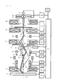
- FIG. 1 is a schematic diagram of a configuration of an optical system of a charged particle beam apparatus according to Example 1.
- FIG. 2 is a schematic diagram of a configuration of an optical system of a charged particle beam apparatus according to Example 2.
- FIG. 3 is a schematic diagram of a configuration of a trajectory monitoring unit according to Example 3.
- FIG. 4 is a schematic diagram of a configuration of a trajectory monitoring unit according to Example 4.
- FIG. 5 is a flowchart of a trajectory correction according to Example 1.
- FIG. 6 is a diagram showing a trajectory of a primary electron in a case where an image shift amount becomes zero in S 005 in FIG. 5 .
- FIG. 7 is a diagram showing a trajectory of the primary electron in a case where the image shift amount becomes zero in S 009 in FIG. 5 .
- FIG. 8 is a flowchart of a trajectory correction according to Example 4.
- FIG. 9 is a diagram showing a configuration of an optical system control unit.
- a charged particle beam apparatus accelerates particles (charged particles) having a charge such as an electron or a positive ion using an electric field and irradiates a sample with a charged particle beam.
- the charged particle beam apparatus uses interaction between the sample and the charged particles and performs observation, analysis, processing operation, or the like of the sample.
- Examples of the charged particle beam apparatus include an electronic microscope, an electron beam lithography system, an ion processing apparatus, an ion microscope, or the like.
- the present invention can be applied to these charged particle beam apparatuses.
- FIG. 1 is a schematic diagram of a configuration of an optical system of a charged particle beam apparatus according to Example 1. First, an operation performed when the primary electron is incident perpendicular to the sample is described.
- a voltage is applied between a cathode 01 and a first anode 02 by a high-voltage control unit 100 and a primary electron (primary charged particle beam) 30 is released at a predetermined emission current.
- an acceleration voltage is applied between the cathode 01 and a second anode 03 by the high-voltage control unit 100 and the primary electron 30 is accelerated and is incident to a lens on a subsequent stage.
- the charged particle beam apparatus includes a plurality of condenser lenses 04 and 06 for controlling a focusing angle and a focusing position of the primary electron 30 .
- the primary electron 30 is converged at a point P 1 on an optical axis 16 by the condenser lens 04 which is controlled by a condenser lens control unit 101 , then, the primary electron 30 passes through an objective aperture 05 , and an unnecessary electron is removed. Then, the primary electron 30 is converged at a point P 2 on the optical axis 16 by the condenser lens 06 which is controlled by the condenser lens control unit 101 .
- the primary electron 30 is incident to an aberration correcting lens 09 which is controlled by an aberration correcting lens control unit 103 and is converged at a point P 3 on the optical axis 16 .
- the primary electron 30 is incident to an objective lens 14 which is controlled by an objective lens control unit 109 , is converged on a sample 15 , and forms a tiny spot.
- a scanning deflector 13 which is controlled by a scanning deflector control unit 107 causes the sample 15 to be scanned in a planar manner with the primary electron 30 .
- a secondary electron 50 which is generated from the sample 15 by the primary electron 30 travels above the objective lens 14 , then, is separated from the primary electron 30 by a crossed electric and magnetic field generating device (EXB) 40 for secondary electron separation, and is incident to a reflector 41 .
- EXB electric and magnetic field generating device
- a tertiary electron 51 is generated from the secondary electron 50 on the reflector 41 .
- the tertiary electron 51 is detected by a detector 42 .
- a signal detected by the detector 42 is transmitted to an image processing apparatus (not shown) and the image processing apparatus forms a sample image corresponding to an irradiation region of the primary electron 30 based on the signal detected by the detector 42 .
- the formed sample image is displayed on an image display unit 112 through an optical system control unit 111 .
- a position of the sample 15 may be controlled by controlling a sample stage (not shown) which is controlled by a stage control unit 110 .
- FIG. 9 is a diagram showing a configuration of the optical system control unit 111 .
- the optical system control unit 111 means an information processing apparatus such as a workstation or a personal computer.
- the optical system control unit 111 includes a central processor, an auxiliary storage device, a main memory, and an input/output device.
- the central processor is configured of a processor (or also referred to as an operation unit) such as a central processing unit (CPU).
- the auxiliary storage device means a hard disk
- the main memory means a memory
- the input/output device means a keyboard and a pointing device (such as a mouse) or a display (image display unit 112 ).
- illustration of these components is omitted.
- the optical system control unit 111 includes a high-voltage condition setting unit 201 , a lens condition setting unit 202 , a deflector condition setting unit 203 , a deflector-operation condition recording unit 113 , a lens-operation condition recording unit 114 , a trajectory calculating unit 115 , and a voltage/current control unit 116 .
- the respective setting units 201 , 202 , and 203 , the trajectory calculating unit 115 , and the voltage/current control unit 116 may be realized by a function of a program which is executed on a computer. That is, processes which are executed by these components may be stored in the memory as a program code and may be realized when the CPU executes the program code. In addition, these components may be realized by hardware, as in a designed integrated circuit, or the like.
- the deflector-operation condition recording unit 113 and the lens-operation condition recording unit 114 are realized by the storage device described above.
- High voltages applied to the cathode 01 , the first anode 02 , and the second anode 03 , and applied voltages and excitation currents of the respective lenses and the respective deflectors are set by the high-voltage condition setting unit 201 , the lens condition setting unit 202 , and the deflector condition setting unit 203 , respectively. Operations of the respective control units 100 to 109 are controlled in accordance with conditions set by the high-voltage condition setting unit 201 , the lens condition setting unit 202 , and the deflector condition setting unit 203 .
- An aberration controlling deflector 08 which is controlled by the deflector control unit 102 is disposed such that the center thereof is positioned at the point P 2 .
- a tilting deflector 11 which is controlled by the deflector control unit 106 is disposed such that the center thereof is positioned at the point P 3 .
- the aberration correcting lens 09 a lens which generates a significant chromatic aberration but has a sufficiently small spherical aberration.
- the primary electron is deflected by the aberration controlling deflector 08 and passes off-axis through the aberration correcting lens 09 . Further, the primary electron is deflected by the tilting deflector 11 in a reverse direction, thereby, passes off-axis through the objective lens 14 , and is tilted and performs irradiation of the sample 15 .
- the primary electron travels through a trajectory 31 (a trajectory below the point P 3 is the same trajectory as that of the primary electron 30 ).
- the trajectory 31 is coincident with a paraxial trajectory.
- the primary electron travels through a trajectory 32 .
- the primary electron passes through a position significantly separated from the point P 3 on an object plane Z 3 of the objective lens 14 .
- a configuration of a trajectory monitoring unit for monitoring the change from the trajectory 31 to the trajectory 32 and a correction method of a trajectory using the configuration will be described.
- the charged particle beam apparatus of the present example includes a trajectory correcting deflector 10 , the tilting deflector 11 , and a trajectory monitoring lens (optical element having a lens action) 12 as a trajectory monitoring unit.
- the tilting deflector 11 is disposed such that the center of the tilting deflector 11 is coincident with an object point P 3 of the objective lens 14 .
- the trajectory monitoring lens 12 is disposed in the vicinity of the tilting deflector 11 with the optical axis as the central axis thereof.
- the trajectory correcting deflector 10 is disposed above both the tilting deflector 11 and the trajectory monitoring lens 12 .
- An applied voltage and an excitation current of the trajectory correcting deflector 10 are controlled by a deflector control unit 104 and an applied voltage and an excitation current of the trajectory monitoring lens 12 are controlled by a monitoring lens control unit 105 .
- the applied voltage and the excitation current of the trajectory monitoring lens 12 become zero when monitoring and correction of the trajectory are not performed.
- the primary electron is deflected by a predetermined angle by the aberration controlling deflector 08 and passes through the aberration correcting lens 09 , the primary electron does not pass through the point P 3 due to the spherical aberration, as described above.
- the primary electron is controlled by the trajectory correcting deflector 10 to pass a point P M which is the center of a lens field distribution of the trajectory monitoring lens 12 and further, the primary electron is controlled to pass the center of the objective lens 14 using the trajectory correcting deflector 10 and the tilting deflector 11 .
- the primary electron travels through the trajectory 30 . Accordingly, correction is performed from the trajectory 32 to the trajectory 30 , and the trajectory 30 passes through the point P 3 .
- the applied voltage and the excitation current are applied to the trajectory correcting deflector 10 which is controlled by the deflector control unit 104 , the trajectory of the primary electron is deflected, and a position on the trajectory monitoring lens 12 , to which the primary electron is incident, is changed.
- the applied voltage and the excitation current of the trajectory correcting deflector 10 are adjusted such that a shift amount of the image of the sample 15 , which is displayed on the image display unit 112 , becomes zero. This adjustment makes it possible for the primary electron to pass through the point P M (a trajectory 33 in FIG. 6 ).
- the applied voltage and the excitation current of the trajectory monitoring lens 12 become zero while the applied voltage and the excitation current with which the primary electron passes through the point P M are set to the trajectory correcting deflector 10 .
- the excitation current of the objective lens 14 is temporally changed on a cyclical basis. Since the primary electron is tilted from the point P M and is incident, the primary electron passes off-axis through the objective lens 14 and the off-axis chromatic aberration is generated. Accordingly, the image of the sample 15 , which is displayed on the image display unit 112 , is temporally shifted.
- the trajectory correcting deflector 10 and the tilting deflector 11 are caused to operate as two-stage deflectors such that a virtual support point of deflection is caused to be coincident with the point P M . Further, the applied voltages and the excitation currents of the trajectory correcting deflector 10 and the tilting deflector 11 are adjusted such that an image shift amount becomes zero. Accordingly, the trajectory of the primary electron that is incident to the center of the objective lens 14 from the central point P 3 of the tilting deflector 11 is realized (a trajectory 34 in FIG. 7 ). Then, when the applied voltage and the excitation current with which the primary electron is deflected by the predetermined angle are accumulated in the tilting deflector 11 , the trajectory 32 becomes the trajectory 30 below the point P 3 .
- the change in the trajectory due to the spherical aberration of the aberration correcting lens 09 is corrected and the trajectory which is incident to the objective lens 14 with the object point P 3 of the objective lens 14 as the support point of the deflection is realized. Accordingly, a tilt image having small shift in an observation position and high resolution can be obtained.
- the present example is characterized in that the applied voltages and the excitation currents of the respective deflectors are adjusted such that the image shift amount becomes zero during the change in the excitation currents of the trajectory monitoring lens 12 and the objective lens 14 and thereby, the trajectory of the primary electron can be the trajectory formed by connecting two points of the object point P 3 of the objective lens 14 and the center of the objective lens 14 .
- this configuration it is possible to remove the change in the trajectory due to the spherical aberration of the aberration correcting lens 09 and it is possible to control the off-axis chromatic aberration, the deflected coma aberration, and the tilt angle with no constraints.
- the trajectory monitoring lens 12 since the trajectory monitoring lens 12 according to the present example operates (turns ON) only when the trajectory of the primary electron is monitored and the applied voltage and the excitation current thereof become zero (that is, turns OFF) when the tilt image is acquired, the lens action and the aberration have no influence on resolution.
- the beam trajectory is monitored and thereby, it is possible to improve reproducibility of the tilt angle or the resolution even in a beam tilt at a small angle.
- FIG. 2 is a schematic diagram of a configuration of a charged particle beam apparatus according to Example 2 of the present invention.
- the same reference signs are attached to the same components as in FIG. 1 and components other than the components which are described below have the same configurations as in FIG. 1 .
- the tilting deflector 11 and the trajectory monitoring lens 12 are disposed at the same elevation.
- the tilting deflector 11 and the trajectory monitoring lens 12 are disposed such that the center of a deflection field distribution of the tilting deflector 11 is disposed at the object point P 3 of the objective lens 14 and a center P M of the lens field distribution of the trajectory monitoring lens 12 is coincident with the object point P 3 of the objective lens 14 .
- the primary electron travels through the trajectory 35 .
- accuracy of the trajectory correction is determined by the accuracy of the coincidence of the virtual support point of the deflection of the trajectory correcting deflector 10 and the tilting deflector 11 with the lens field center point P M of the trajectory monitoring lens 12 .
- the tilting deflector 11 since only the tilting deflector 11 is used when the primary electron is incident to the center of the objective lens 14 from the object point P 3 of the objective lens 14 , it is possible to correct the trajectory with highest accuracy and it is possible to correct aberration while the positional shift during the beam tilt of the primary electron is prevented.
- FIG. 3 is a schematic diagram of a configuration of a trajectory monitoring unit according to Example 3 of the present invention. According to the present example, the most preferred example for realizing the configuration described in Example 2 is described.
- the tilting deflector 11 and the trajectory monitoring lens 12 are configured as a deflection unit 220 which is formed to have four magnetic poles.
- the deflection unit 220 includes four deflectors 211 a , 211 b , 211 c , and 211 d .
- Each of the four deflectors 211 a , 211 b , 211 c , and 211 d includes a pole in which a coil is wound.
- currents having the same size flow through the coils wound in the poles of the four deflectors 211 a , 211 b , 211 c , and 211 d and the currents flows, in a reverse direction, through the coils of the deflectors that face each other.
- the deflector 211 a and the deflector 211 c act as N poles
- the deflector 211 b and the deflector 211 d act as S poles
- the deflection unit 220 acts as a magnetic field-type quadrupole lens.
- currents having the same size flow through the coils of the deflectors which face each other, in the same direction.
- the deflector 211 a acts as the N pole
- the deflector 211 c acts as the S pole
- the deflection unit 220 acts as a deflector.
- the deflection unit 220 includes both the quadrupole lens and the deflector.
- a quadrupole field has the same central position as the magnetic field distribution of the deflection field.
- a deflector having no magnetic pole may be used as an alternative example.
- a coil is wound by being divided into four blocks which are orthogonal to each other and the same quadrupole lens action is obtained when the currents are applied to the blocks as described above.
- it is desirable that the coil is wound in a saddle shape.
- an electric field-type deflection unit which is formed by four electrodes may be used instead of the magnetic field-type deflection unit described above.
- the present example is characterized in that, when the direction of the current and polarity of the voltage which are applied to the quadrupoles or the four blocks are changed, it is possible to switch between the quadrupole lens action and the deflection action.
- the number of necessary power sources is two and the two power sources that operate the deflectors in an X direction and in a Y direction are sufficient.
- FIG. 4 is a schematic diagram of a configuration of a trajectory monitoring unit according to Example 4 of the present invention. According to the present example, a case in which the trajectory monitoring unit is applied to a conventional aberration corrector (for example, PTL 3 and PTL 4) is described.
- a conventional aberration corrector for example, PTL 3 and PTL 4
- the aberration corrector 305 corrects an aberration generated in the optical system of the charged particle beam apparatus.
- Two stages of trajectory monitoring units 302 and 304 are disposed above the aberration corrector 305 .
- two stages of trajectory correcting deflectors 301 and 303 are disposed above the aberration corrector 305 .
- the trajectory correcting deflector 303 on the lower stage side is disposed at the same elevation as the trajectory monitoring unit 302 on the upper stage side so as to have a center in common with the trajectory monitoring unit 302 on the upper stage side.
- the trajectory correcting deflector 301 on the upper stage side is disposed above the trajectory correcting deflector 303 on the lower stage side and the trajectory monitoring unit 302 of the upper stage side.
- the primary electron 306 is caused to pass through the center of the trajectory monitoring unit 302 on the upper stage side using the trajectory correcting deflector 301 on the upper stage side, following the procedure described in Example 1 and further is caused to pass through the center of the trajectory monitoring unit 304 on the lower stage side using the trajectory correcting deflector 303 on the lower stage side. Accordingly, the primary electron travels through a trajectory 306 . As a result, the primary electron is incident to the aberration corrector 305 through the trajectory formed by connecting two points of the centers of the trajectory monitoring lens 302 on the upper stage side and the trajectory monitoring lens 304 on the lower stage side.
- the trajectory correcting deflector 301 on the upper stage side is changed, it is possible to correct the trajectory which is incident to the aberration corrector 305 .
- the trajectory correction operation only has to be performed with respect to the change in the incident trajectory and there is no need to perform adjustment of the aberration corrector 305 again. Therefore, it is possible to simplify the adjustment procedure performed in a case where the electron trajectory incident to the aberration corrector is changed.
- the two stages of the trajectory monitoring units 302 and 304 and the two stages of the trajectory correcting deflectors 301 and 303 described in the present example are disposed on any optical element and thereby it is possible to correct the incident trajectory.
- FIG. 5 is a flowchart of the trajectory correction according to Example 1.
- step S 001 a predetermined current and voltage is applied to the condenser lens 04 , the condenser lens 06 , the aberration correcting lens 09 , and the objective lens 14 and optical conditions are set. At this time, the respective lenses are controlled by the lens condition setting unit 202 of the optical system control unit 111 .
- step S 002 the tilt angle of the beam of the primary electron is determined and an aberration for correction is generated.
- the applied voltage and the excitation current of the aberration controlling deflector 08 are set, the beam of the primary electron is deflected by the predetermined angle, and the deflected beam is caused to pass through the aberration correcting lens 09 .
- the aberration controlling deflector 08 is controlled by the deflector condition setting unit 203 of the optical system control unit 111 .
- step S 003 the current and voltage are applied to the trajectory monitoring lens 12 and the applied voltage and the excitation current of the trajectory monitoring lens 12 are temporally changed (first control mode).
- the lens condition setting unit 202 of the optical system control unit 111 controls the trajectory monitoring lens 12 through the monitoring lens control unit 105 .
- step S 004 the applied voltage and the excitation current of the trajectory correcting deflector 10 are set and the trajectory of the primary electron is deflected.
- the deflector condition setting unit 203 of the optical system control unit 111 controls the trajectory correcting deflector 10 through the deflector control unit 104 .
- step S 005 it is determined whether the image shift amount of the image of the sample 15 is zero. If the image shift amount is not zero, the process returns to step S 004 and the applied voltage and the excitation current of the trajectory correcting deflector 10 are changed. In the case where the image shift amount is zero, the applied voltage and the excitation current of the trajectory correcting deflector 10 , with which the image shift amount becomes zero, are set and the primary electron is caused to pass through the point P M . At this time, the primary electron travels through the trajectory 33 in FIG. 6 . The optical system control unit 111 causes the applied voltage and the excitation current of the trajectory correcting deflector 10 , with which the image shift amount becomes zero, to be recorded in the deflector-operation condition recording unit 113 .
- the setting of the applied voltage and the excitation current of the trajectory correcting deflector 10 in step S 004 and the determination of whether the image shift amount is zero in step S 005 may be performed by an operator or may be automatically performed by the optical system control unit 111 .
- the voltage/current control unit 116 of the optical system control unit 111 automatically calculates the image shift amount and the applied voltage and the excitation current of the trajectory correcting deflector 10 are changed such that the image shift amount becomes zero.
- a technology disclosed in PTL 5 is applied to the voltage/current control unit 116 and thereby, it is possible to perform a process in which the applied voltage and the excitation current of the trajectory correcting deflector 10 are automatically changed such that the image shift amount becomes zero.
- step S 006 the applied voltage and the excitation current of the trajectory monitoring lens 12 becomes zero.
- step S 007 the excitation current flowing through the objective lens 14 is temporally changed (second control mode).
- step S 008 the trajectory correcting deflector 10 and the tilting deflector 11 which are controlled by the deflector control units 104 and 106 are caused to operate as the two-stage deflectors and the applied voltages and the excitation currents of the trajectory correcting deflector 10 and the tilting deflector 11 are set with the virtual support point of the deflection as the point P M .
- the applied voltage and the excitation current which are adjusted in step S 005 are accumulated in the trajectory correcting deflector 10 .
- step S 009 it is determined whether the image shift amount of the image of the sample 15 is zero. If the image shift amount is not zero, the process returns to step S 008 and the applied voltages and the excitation currents of the trajectory correcting deflector 10 and the tilting deflector 11 are changed. In the case where the image shift amount is zero, the optical system control unit 111 causes the applied voltages and the excitation currents of the trajectory correcting deflector 10 and the tilting deflector 11 , with which the image shift amount becomes zero, to be recorded in the deflector-operation condition recording unit 113 . At this time, the primary electron travels through the trajectory 34 in FIG. 7 and is incident to the center of the objective lens 14 from the point P 3 .
- the setting of the applied voltages and the excitation currents of the trajectory correcting deflector 10 and the tilting deflector 11 in step S 008 and the determination of whether the image shift amount is zero in step S 009 may be performed by an operator or may be automatically performed by the optical system control unit 111 .
- the voltage/current control unit 116 of the optical system control unit 111 automatically calculates the image shift amount and the applied voltages and the excitation currents of the trajectory correcting deflector 10 and the tilting deflector 11 are changed such that the image shift amount becomes zero.
- step S 010 the applied voltage and the excitation current which are used for deflecting the primary electron by the predetermined angle are accumulated to the tilting deflector 11 in addition to the aberration corrector and the excitation current for trajectory correction, which are obtained in step S 009 , and the primary electron is tilted.
- step S 011 field curvature and astigmatism which are generated in step S 010 are corrected by adjusting the excitation current flowing through the objective lens 14 and a stigmator 07 .
- the excitation current of the stigmator 07 is controlled by a stigmator control unit 108 .
- the optical system control unit 111 causes the respective adjustment amounts to be recorded in the lens-operation condition recording unit 114 .
- step S 012 the charged particle beam apparatus acquires a tilt image under imaging conditions set in the process to step S 011 . Then, in step S 013 , it is determined whether or not the change in the tilt angle and the tilt direction is performed. In the case of the change, the process returns to step S 002 . In a case where the process returns to step S 002 , an applied voltage and an excitation current of the aberration controlling deflector 08 are newly set. It is possible to acquire the tilt image through the above flow after the trajectory correction.
- the primary electron may be deflected using only the tilting deflector 11 and the applied voltage and the excitation current may be adjusted such that the image shift amount becomes zero.
- the applied voltages and the excitation currents recorded in the deflector-operation condition recording unit 113 and the lens-operation condition recording unit 114 in the optical system control unit 111 may be organized in a table.
- information of the applied voltage and the excitation current recorded in the deflector-operation condition recording unit 113 and the lens-operation condition recording unit 114 may be recorded in a predetermined storage unit for each of the optical condition, the tilt angle, and the tilt direction of a lens, in a table structure. It is possible to simplify the adjustment during tilting of the primary electron beam by using the information in the table structure.
- the applied voltage and the excitation current recorded in the deflector-operation condition recording unit 113 and the lens-operation condition recording unit 114 may be delivered to the trajectory calculating unit 115 and trajectory calculation may be performed.
- the trajectory calculating unit 115 computes an off-axis amount from the optical axis 16 and an incident angle which are obtained when the primary electron passes through the center of the trajectory correcting deflector 10 , for each lens condition. For example, permissible amounts of the off-axis amount and the incident angle which satisfy performance of the apparatus are set in advance.
- FIG. 8 is a flowchart of the trajectory correction according to Example 4.
- the aberration corrector 305 finishes the adjustment of the primary electron which is perpendicularly incident along the optical axis.
- an applied voltage and an excitation current are set to the trajectory monitoring unit 302 on the upper stage side and the applied voltage and the excitation current are temporally changed in step S 101 (a third control method).
- step S 102 the applied voltage and the excitation current of the trajectory correcting deflector 301 on the upper stage side are set and the primary electron is deflected.
- step S 103 it is determined whether the image shift amount of the image of the sample 15 is zero. If the image shift amount is zero, the process returns to step S 102 and the applied voltage and the excitation current of the trajectory correcting deflector 301 on the upper stage side are changed. In the case where the image shift amount is zero, the process proceeds to step S 104 .
- step S 104 the applied voltage and the excitation current of the trajectory monitoring unit 302 on the upper stage side becomes zero.
- step S 105 the applied voltage and the excitation current of the trajectory monitoring unit 304 on the lower stage side are set and the applied voltage and the excitation current are temporally changed (fourth control mode).
- step S 106 the applied voltage and the excitation current of the trajectory correcting deflector 303 on the lower stage side are set.
- step S 107 it is determined whether the image shift amount of the image of the sample 15 is zero. If the image shift amount is zero, the process returns to step S 106 and the applied voltage and the excitation current of the trajectory correcting deflector 303 on the lower stage side are changed. In the case where the image shift amount is zero, the process proceeds to step S 108 .
- step S 108 if the applied voltage and the excitation current of the trajectory monitoring unit 304 on the lower stage side is zero, the trajectory correction according to Example 4 is ended.
- the trajectory of the primary electron after the trajectory correction becomes the trajectory 306 shown in FIG. 4 . That is, the primary electron is incident to the aberration corrector 305 through a trajectory formed by connecting the two points of the center of the trajectory monitoring unit 302 on the upper stage side and the center of the trajectory monitoring unit 304 on the lower stage side.
- Example 2 Similar to the case of Example 1, it is possible to automatically perform the trajectory correction also in the cases of Example 2 to Example 4. In addition, it is needless to say that it is possible to compute an off-axis amount from the optical axis and an incident angle of a trajectory which is incident to a trajectory correcting deflector.
- steps S 102 , S 103 , S 106 , and S 107 in FIG. 8 may be automatically performed.
- the voltage/current control unit 116 adjusts the applied voltage and the excitation current of the trajectory correcting deflector 301 on the upper stage side such that the image shift amount of the sample image becomes zero in the third control mode and adjusts the applied voltage and the excitation current of the trajectory correcting deflector 303 on the lower stage side such that the image shift amount of the sample image becomes zero in the fourth control mode.
- the present invention is not limited to the examples described above and includes various modification examples.
- the examples described above are described in detail in order to provide an easy description of the present invention and the present invention is not limited to the example which includes the entire configuration described above.
- a part of a configuration of a certain example can be replaced with a configuration of another example and further it is possible to add a configuration of a certain example to a configuration of another example.
- addition, removal, and replacement of another configuration can be performed.
- control-process lines and information-process lines in the drawings are illustrated as necessary for the description and the control-process lines and information-process lines on the product are not all illustrated. All of the configurations may be connected to each other.
Landscapes
- Chemical & Material Sciences (AREA)
- Analytical Chemistry (AREA)
- Electron Sources, Ion Sources (AREA)
- Engineering & Computer Science (AREA)
- Computer Vision & Pattern Recognition (AREA)
Abstract
Description
- 01 cathode
- 02 first anode
- 03 second anode
- 04 condenser lens
- 05 movable objective aperture
- 06 condenser lens
- 07 stigmator
- 08 aberration controlling deflector
- 09 aberration correcting lens
- 10 trajectory correcting deflector
- 11 tilting deflector
- 12 trajectory monitoring lens
- 13 scanning deflector
- 14 objective lens
- 15 sample
- 16 optical axis
- 30 trajectory
- 31 trajectory
- 32 trajectory
- 33 trajectory
- 34 trajectory
- 35 trajectory
- 40 crossed electric and magnetic field generating device (EXB)
- 41 reflector
- 42 detector
- 100 high-voltage control unit
- 101 condenser lens control unit
- 102 deflector control unit
- 103 aberration correcting lens control unit
- 104 deflector control unit
- 105 monitoring lens control unit
- 106 deflector control unit
- 107 deflector control unit
- 108 stigmator control unit
- 109 objective lens control unit
- 110 stage control unit
- 111 optical system control unit
- 112 image display unit
- 113 deflector operation recording unit
- 114 lens operation recording unit
- 115 trajectory calculating unit
- 116 voltage/current control unit
- 201 high-voltage condition setting unit
- 202 lens condition setting unit
- 203 deflector condition setting unit
- 211 a deflector
- 211 b deflector
- 211 c deflector
- 211 d deflector
- 220 deflection unit
- 301 trajectory correcting deflector on the upper stage side
- 302 trajectory monitoring lens on the upper stage side
- 303 trajectory correcting deflector on the lower stage side
- 304 trajectory monitoring lens on the lower stage side
- 305 aberration corrector
- 306 trajectory
Claims (13)
Applications Claiming Priority (3)
| Application Number | Priority Date | Filing Date | Title |
|---|---|---|---|
| JP2013011241A JP6134145B2 (en) | 2013-01-24 | 2013-01-24 | Charged particle beam apparatus and trajectory correction method in charged particle beam apparatus |
| JP2013-011241 | 2013-01-24 | ||
| PCT/JP2014/051070 WO2014115708A1 (en) | 2013-01-24 | 2014-01-21 | Charged particle beam apparatus and trajectory correction method in charged particle beam apparatus |
Publications (2)
| Publication Number | Publication Date |
|---|---|
| US20150357155A1 US20150357155A1 (en) | 2015-12-10 |
| US9484181B2 true US9484181B2 (en) | 2016-11-01 |
Family
ID=51227499
Family Applications (1)
| Application Number | Title | Priority Date | Filing Date |
|---|---|---|---|
| US14/760,053 Active US9484181B2 (en) | 2013-01-24 | 2014-01-21 | Charged particle beam apparatus and trajectory correction method in charged particle beam apparatus |
Country Status (3)
| Country | Link |
|---|---|
| US (1) | US9484181B2 (en) |
| JP (1) | JP6134145B2 (en) |
| WO (1) | WO2014115708A1 (en) |
Families Citing this family (10)
| Publication number | Priority date | Publication date | Assignee | Title |
|---|---|---|---|---|
| JP6438780B2 (en) * | 2015-02-02 | 2018-12-19 | 株式会社日立ハイテクノロジーズ | Charged particle beam apparatus and aberration correction method |
| US11861716B1 (en) | 2016-10-27 | 2024-01-02 | State Farm Mutual Automobile Insurance Company | Systems and methods for utilizing electricity monitoring devices to reconstruct an electrical event |
| US10157727B2 (en) * | 2017-03-02 | 2018-12-18 | Fei Company | Aberration measurement in a charged particle microscope |
| WO2018163240A1 (en) * | 2017-03-06 | 2018-09-13 | 株式会社日立ハイテクノロジーズ | Charged particle beam device |
| JP6932050B2 (en) * | 2017-09-01 | 2021-09-08 | 株式会社日立ハイテク | Scanning electron microscope |
| DE102017220398B3 (en) * | 2017-11-15 | 2019-02-28 | Carl Zeiss Microscopy Gmbh | Method for adjusting a particle beam microscope |
| US11508551B2 (en) * | 2018-12-14 | 2022-11-22 | Kla Corporation | Detection and correction of system responses in real-time |
| JP6737539B2 (en) * | 2019-02-25 | 2020-08-12 | 株式会社日立ハイテク | Charged particle beam device |
| JP2020149767A (en) | 2019-03-11 | 2020-09-17 | 株式会社日立ハイテク | Charged particle beam device |
| CN116798841A (en) * | 2023-07-14 | 2023-09-22 | 无锡亘芯悦科技有限公司 | Scanning electron beam imaging system with adjustable beam opening angle and electron beam control method |
Citations (9)
| Publication number | Priority date | Publication date | Assignee | Title |
|---|---|---|---|---|
| JPH0233843A (en) | 1988-07-25 | 1990-02-05 | Hitachi Ltd | Scanning electronic microscope |
| US5838011A (en) * | 1996-05-21 | 1998-11-17 | U.S. Philips Corporation | Correction device for the correction of lens aberrations in particle-optical apparatus |
| JP2001015055A (en) | 1999-04-15 | 2001-01-19 | Applied Materials Inc | Charged particle beam column |
| US20020179851A1 (en) | 2001-05-30 | 2002-12-05 | Mitsugu Sato | Charged particle beam alignment method and charged particle beam apparatus |
| JP2002352758A (en) | 2001-05-30 | 2002-12-06 | Hitachi Ltd | Adjusting method of charged particle beam, and charged particle beam system |
| US6627890B2 (en) * | 1999-03-31 | 2003-09-30 | Advantest Corp. | Particle beam apparatus for tilted observation of a specimen |
| US20050285036A1 (en) | 2004-06-28 | 2005-12-29 | Hitachi High-Technologies Corporation | Charged particle beam emitting device and method for adjusting the optical axis |
| US20060033037A1 (en) | 2004-08-10 | 2006-02-16 | Takeshi Kawasaki | Charged particle beam column |
| US7705300B2 (en) * | 2004-04-23 | 2010-04-27 | Hitachi High-Technologies Corporation | Charged particle beam adjusting method and charged particle beam apparatus |
-
2013
- 2013-01-24 JP JP2013011241A patent/JP6134145B2/en active Active
-
2014
- 2014-01-21 US US14/760,053 patent/US9484181B2/en active Active
- 2014-01-21 WO PCT/JP2014/051070 patent/WO2014115708A1/en active Application Filing
Patent Citations (13)
| Publication number | Priority date | Publication date | Assignee | Title |
|---|---|---|---|---|
| JPH0233843A (en) | 1988-07-25 | 1990-02-05 | Hitachi Ltd | Scanning electronic microscope |
| US4983832A (en) | 1988-07-25 | 1991-01-08 | Hitachi, Ltd. | Scanning electron microscope |
| US5838011A (en) * | 1996-05-21 | 1998-11-17 | U.S. Philips Corporation | Correction device for the correction of lens aberrations in particle-optical apparatus |
| US6627890B2 (en) * | 1999-03-31 | 2003-09-30 | Advantest Corp. | Particle beam apparatus for tilted observation of a specimen |
| US6614026B1 (en) | 1999-04-15 | 2003-09-02 | Applied Materials, Inc. | Charged particle beam column |
| JP2001015055A (en) | 1999-04-15 | 2001-01-19 | Applied Materials Inc | Charged particle beam column |
| JP2002352758A (en) | 2001-05-30 | 2002-12-06 | Hitachi Ltd | Adjusting method of charged particle beam, and charged particle beam system |
| US20020179851A1 (en) | 2001-05-30 | 2002-12-05 | Mitsugu Sato | Charged particle beam alignment method and charged particle beam apparatus |
| US7705300B2 (en) * | 2004-04-23 | 2010-04-27 | Hitachi High-Technologies Corporation | Charged particle beam adjusting method and charged particle beam apparatus |
| US20050285036A1 (en) | 2004-06-28 | 2005-12-29 | Hitachi High-Technologies Corporation | Charged particle beam emitting device and method for adjusting the optical axis |
| JP2006012664A (en) | 2004-06-28 | 2006-01-12 | Hitachi High-Technologies Corp | Charged particle beam device and its collimation method |
| US20060033037A1 (en) | 2004-08-10 | 2006-02-16 | Takeshi Kawasaki | Charged particle beam column |
| JP2006054074A (en) | 2004-08-10 | 2006-02-23 | Hitachi High-Technologies Corp | Charged particle beam column |
Non-Patent Citations (1)
| Title |
|---|
| International Search Report (PCT/ISA/210) dated Feb. 18, 2014 with English-language translation (two (2) pages). |
Also Published As
| Publication number | Publication date |
|---|---|
| JP2014143096A (en) | 2014-08-07 |
| JP6134145B2 (en) | 2017-05-24 |
| US20150357155A1 (en) | 2015-12-10 |
| WO2014115708A1 (en) | 2014-07-31 |
Similar Documents
| Publication | Publication Date | Title |
|---|---|---|
| US9484181B2 (en) | Charged particle beam apparatus and trajectory correction method in charged particle beam apparatus | |
| US10446361B2 (en) | Aberration correction method, aberration correction system, and charged particle beam apparatus | |
| JP4988216B2 (en) | Charged particle beam equipment equipped with an aberration correction device | |
| JP6554288B2 (en) | Charged particle beam equipment | |
| JP4620981B2 (en) | Charged particle beam equipment | |
| US9053900B2 (en) | Apparatus and methods for high-resolution electron beam imaging | |
| JP5277250B2 (en) | Charged particle beam application apparatus and geometric aberration measuring method thereof | |
| JP4881661B2 (en) | Charged particle beam equipment | |
| JP6037693B2 (en) | Charged particle beam equipment | |
| JP6404736B2 (en) | Compound charged particle beam system | |
| US10573489B2 (en) | Charged particle beam device and optical-axis adjusting method thereof | |
| JP5331893B2 (en) | Scanning charged particle beam apparatus and chromatic spherical aberration correction method | |
| JP5993668B2 (en) | Charged particle beam equipment | |
| US20180366295A1 (en) | Distortion Correction Method and Electron Microscope | |
| CN115863128A (en) | Focusing deflection module for critical dimension measuring device and electron beam column | |
| JP6737539B2 (en) | Charged particle beam device | |
| WO2021100172A1 (en) | Charged particle beam device and aberration correction method | |
| JP5204277B2 (en) | Charged particle beam equipment | |
| US20180025886A1 (en) | Charged Particle Beam Device and Aberration Corrector | |
| JP2010251218A (en) | Charged particle beam device | |
| CN117672786A (en) | Magnetic multipole device, charged particle beam apparatus and method of influencing a charged particle beam propagating along an optical axis | |
| JP2011040256A (en) | Scanning charged particle beam device |
Legal Events
| Date | Code | Title | Description |
|---|---|---|---|
| AS | Assignment |
Owner name: HITACHI HIGH-TECHNOLOGIES CORPORATION, JAPAN Free format text: ASSIGNMENT OF ASSIGNORS INTEREST;ASSIGNORS:DOHI, HIDETO;IKEGAMI, AKIRA;KAZUMI, HIDEYUKI;REEL/FRAME:036046/0464 Effective date: 20150611 |
|
| STCF | Information on status: patent grant |
Free format text: PATENTED CASE |
|
| AS | Assignment |
Owner name: HITACHI HIGH-TECH CORPORATION, JAPAN Free format text: CHANGE OF NAME AND ADDRESS;ASSIGNOR:HITACHI HIGH-TECHNOLOGIES CORPORATION;REEL/FRAME:052259/0227 Effective date: 20200212 |
|
| MAFP | Maintenance fee payment |
Free format text: PAYMENT OF MAINTENANCE FEE, 4TH YEAR, LARGE ENTITY (ORIGINAL EVENT CODE: M1551); ENTITY STATUS OF PATENT OWNER: LARGE ENTITY Year of fee payment: 4 |
|
| MAFP | Maintenance fee payment |
Free format text: PAYMENT OF MAINTENANCE FEE, 8TH YEAR, LARGE ENTITY (ORIGINAL EVENT CODE: M1552); ENTITY STATUS OF PATENT OWNER: LARGE ENTITY Year of fee payment: 8 |