US9461614B2 - Asymmetric unbalanced acoustically coupled resonators for spurious mode suppression - Google Patents
Asymmetric unbalanced acoustically coupled resonators for spurious mode suppression Download PDFInfo
- Publication number
- US9461614B2 US9461614B2 US14/067,908 US201314067908A US9461614B2 US 9461614 B2 US9461614 B2 US 9461614B2 US 201314067908 A US201314067908 A US 201314067908A US 9461614 B2 US9461614 B2 US 9461614B2
- Authority
- US
- United States
- Prior art keywords
- resonator
- core
- piezoelectric core
- electrode
- electrodes
- Prior art date
- Legal status (The legal status is an assumption and is not a legal conclusion. Google has not performed a legal analysis and makes no representation as to the accuracy of the status listed.)
- Expired - Fee Related, expires
Links
- 230000001629 suppression Effects 0.000 title description 8
- 230000005611 electricity Effects 0.000 claims description 25
- 230000008878 coupling Effects 0.000 claims description 17
- 238000010168 coupling process Methods 0.000 claims description 17
- 238000005859 coupling reaction Methods 0.000 claims description 17
- 238000004891 communication Methods 0.000 claims description 11
- 230000004044 response Effects 0.000 description 28
- 239000011295 pitch Substances 0.000 description 25
- 238000006073 displacement reaction Methods 0.000 description 20
- 238000000034 method Methods 0.000 description 19
- 238000013461 design Methods 0.000 description 14
- 230000005684 electric field Effects 0.000 description 14
- 238000003860 storage Methods 0.000 description 12
- 238000010586 diagram Methods 0.000 description 8
- 230000015654 memory Effects 0.000 description 8
- 239000004065 semiconductor Substances 0.000 description 7
- 230000008569 process Effects 0.000 description 6
- 230000006870 function Effects 0.000 description 5
- 238000004519 manufacturing process Methods 0.000 description 5
- 239000000463 material Substances 0.000 description 4
- PXHVJJICTQNCMI-UHFFFAOYSA-N Nickel Chemical compound [Ni] PXHVJJICTQNCMI-UHFFFAOYSA-N 0.000 description 3
- 239000000203 mixture Substances 0.000 description 3
- BASFCYQUMIYNBI-UHFFFAOYSA-N platinum Chemical compound [Pt] BASFCYQUMIYNBI-UHFFFAOYSA-N 0.000 description 3
- VYPSYNLAJGMNEJ-UHFFFAOYSA-N silicon dioxide Inorganic materials O=[Si]=O VYPSYNLAJGMNEJ-UHFFFAOYSA-N 0.000 description 3
- 239000000758 substrate Substances 0.000 description 3
- 239000011651 chromium Substances 0.000 description 2
- 230000008602 contraction Effects 0.000 description 2
- 239000010949 copper Substances 0.000 description 2
- 239000013078 crystal Substances 0.000 description 2
- 239000010931 gold Substances 0.000 description 2
- 229910052451 lead zirconate titanate Inorganic materials 0.000 description 2
- 230000004048 modification Effects 0.000 description 2
- 238000012986 modification Methods 0.000 description 2
- 230000007935 neutral effect Effects 0.000 description 2
- 230000003287 optical effect Effects 0.000 description 2
- 229910052853 topaz Inorganic materials 0.000 description 2
- WKBPZYKAUNRMKP-UHFFFAOYSA-N 1-[2-(2,4-dichlorophenyl)pentyl]1,2,4-triazole Chemical compound C=1C=C(Cl)C=C(Cl)C=1C(CCC)CN1C=NC=N1 WKBPZYKAUNRMKP-UHFFFAOYSA-N 0.000 description 1
- WSMQKESQZFQMFW-UHFFFAOYSA-N 5-methyl-pyrazole-3-carboxylic acid Chemical compound CC1=CC(C(O)=O)=NN1 WSMQKESQZFQMFW-UHFFFAOYSA-N 0.000 description 1
- PIGFYZPCRLYGLF-UHFFFAOYSA-N Aluminum nitride Chemical compound [Al]#N PIGFYZPCRLYGLF-UHFFFAOYSA-N 0.000 description 1
- ZOXJGFHDIHLPTG-UHFFFAOYSA-N Boron Chemical compound [B] ZOXJGFHDIHLPTG-UHFFFAOYSA-N 0.000 description 1
- VYZAMTAEIAYCRO-UHFFFAOYSA-N Chromium Chemical compound [Cr] VYZAMTAEIAYCRO-UHFFFAOYSA-N 0.000 description 1
- RYGMFSIKBFXOCR-UHFFFAOYSA-N Copper Chemical compound [Cu] RYGMFSIKBFXOCR-UHFFFAOYSA-N 0.000 description 1
- 229910052691 Erbium Inorganic materials 0.000 description 1
- 229910003327 LiNbO3 Inorganic materials 0.000 description 1
- ZOKXTWBITQBERF-UHFFFAOYSA-N Molybdenum Chemical compound [Mo] ZOKXTWBITQBERF-UHFFFAOYSA-N 0.000 description 1
- BQCADISMDOOEFD-UHFFFAOYSA-N Silver Chemical compound [Ag] BQCADISMDOOEFD-UHFFFAOYSA-N 0.000 description 1
- XLOMVQKBTHCTTD-UHFFFAOYSA-N Zinc monoxide Chemical compound [Zn]=O XLOMVQKBTHCTTD-UHFFFAOYSA-N 0.000 description 1
- 239000000956 alloy Substances 0.000 description 1
- 229910045601 alloy Inorganic materials 0.000 description 1
- 230000004075 alteration Effects 0.000 description 1
- XAGFODPZIPBFFR-UHFFFAOYSA-N aluminium Chemical compound [Al] XAGFODPZIPBFFR-UHFFFAOYSA-N 0.000 description 1
- 229910052782 aluminium Inorganic materials 0.000 description 1
- 238000013459 approach Methods 0.000 description 1
- 230000002238 attenuated effect Effects 0.000 description 1
- 230000005540 biological transmission Effects 0.000 description 1
- 229910052796 boron Inorganic materials 0.000 description 1
- 239000003990 capacitor Substances 0.000 description 1
- 229910052804 chromium Inorganic materials 0.000 description 1
- 229910052681 coesite Inorganic materials 0.000 description 1
- 238000004590 computer program Methods 0.000 description 1
- 238000010276 construction Methods 0.000 description 1
- 229910052802 copper Inorganic materials 0.000 description 1
- 229910052906 cristobalite Inorganic materials 0.000 description 1
- 230000007423 decrease Effects 0.000 description 1
- 230000003247 decreasing effect Effects 0.000 description 1
- 230000000694 effects Effects 0.000 description 1
- 238000000609 electron-beam lithography Methods 0.000 description 1
- 238000005516 engineering process Methods 0.000 description 1
- UYAHIZSMUZPPFV-UHFFFAOYSA-N erbium Chemical compound [Er] UYAHIZSMUZPPFV-UHFFFAOYSA-N 0.000 description 1
- 238000005530 etching Methods 0.000 description 1
- PCHJSUWPFVWCPO-UHFFFAOYSA-N gold Chemical compound [Au] PCHJSUWPFVWCPO-UHFFFAOYSA-N 0.000 description 1
- 229910052737 gold Inorganic materials 0.000 description 1
- 229910052909 inorganic silicate Inorganic materials 0.000 description 1
- HFGPZNIAWCZYJU-UHFFFAOYSA-N lead zirconate titanate Chemical compound [O-2].[O-2].[O-2].[O-2].[O-2].[Ti+4].[Zr+4].[Pb+2] HFGPZNIAWCZYJU-UHFFFAOYSA-N 0.000 description 1
- GQYHUHYESMUTHG-UHFFFAOYSA-N lithium niobate Chemical compound [Li+].[O-][Nb](=O)=O GQYHUHYESMUTHG-UHFFFAOYSA-N 0.000 description 1
- 230000007774 longterm Effects 0.000 description 1
- 229910052750 molybdenum Inorganic materials 0.000 description 1
- 239000011733 molybdenum Substances 0.000 description 1
- 229910052759 nickel Inorganic materials 0.000 description 1
- 230000008520 organization Effects 0.000 description 1
- 238000000206 photolithography Methods 0.000 description 1
- 238000001020 plasma etching Methods 0.000 description 1
- 229910052697 platinum Inorganic materials 0.000 description 1
- 239000010453 quartz Substances 0.000 description 1
- 230000009467 reduction Effects 0.000 description 1
- 230000002441 reversible effect Effects 0.000 description 1
- 229910052706 scandium Inorganic materials 0.000 description 1
- SIXSYDAISGFNSX-UHFFFAOYSA-N scandium atom Chemical compound [Sc] SIXSYDAISGFNSX-UHFFFAOYSA-N 0.000 description 1
- 239000000377 silicon dioxide Substances 0.000 description 1
- 229910052709 silver Inorganic materials 0.000 description 1
- 239000004332 silver Substances 0.000 description 1
- 238000004088 simulation Methods 0.000 description 1
- 229910052682 stishovite Inorganic materials 0.000 description 1
- 238000006467 substitution reaction Methods 0.000 description 1
- 239000011031 topaz Substances 0.000 description 1
- 238000012546 transfer Methods 0.000 description 1
- 238000013519 translation Methods 0.000 description 1
- 229910052905 tridymite Inorganic materials 0.000 description 1
- WFKWXMTUELFFGS-UHFFFAOYSA-N tungsten Chemical compound [W] WFKWXMTUELFFGS-UHFFFAOYSA-N 0.000 description 1
- 229910052721 tungsten Inorganic materials 0.000 description 1
- 239000010937 tungsten Substances 0.000 description 1
- 238000012795 verification Methods 0.000 description 1
- 235000012431 wafers Nutrition 0.000 description 1
- 238000003631 wet chemical etching Methods 0.000 description 1
Images


Classifications
-
- H—ELECTRICITY
- H03—ELECTRONIC CIRCUITRY
- H03H—IMPEDANCE NETWORKS, e.g. RESONANT CIRCUITS; RESONATORS
- H03H9/00—Networks comprising electromechanical or electro-acoustic elements; Electromechanical resonators
- H03H9/15—Constructional features of resonators consisting of piezoelectric or electrostrictive material
- H03H9/17—Constructional features of resonators consisting of piezoelectric or electrostrictive material having a single resonator
-
- H01L41/047—
-
- H—ELECTRICITY
- H03—ELECTRONIC CIRCUITRY
- H03H—IMPEDANCE NETWORKS, e.g. RESONANT CIRCUITS; RESONATORS
- H03H9/00—Networks comprising electromechanical or electro-acoustic elements; Electromechanical resonators
- H03H9/02—Details
- H03H9/02007—Details of bulk acoustic wave devices
- H03H9/02157—Dimensional parameters, e.g. ratio between two dimension parameters, length, width or thickness
-
- H—ELECTRICITY
- H03—ELECTRONIC CIRCUITRY
- H03H—IMPEDANCE NETWORKS, e.g. RESONANT CIRCUITS; RESONATORS
- H03H9/00—Networks comprising electromechanical or electro-acoustic elements; Electromechanical resonators
- H03H9/02—Details
- H03H9/125—Driving means, e.g. electrodes, coils
- H03H9/13—Driving means, e.g. electrodes, coils for networks consisting of piezoelectric or electrostrictive materials
-
- H—ELECTRICITY
- H03—ELECTRONIC CIRCUITRY
- H03H—IMPEDANCE NETWORKS, e.g. RESONANT CIRCUITS; RESONATORS
- H03H9/00—Networks comprising electromechanical or electro-acoustic elements; Electromechanical resonators
- H03H9/46—Filters
- H03H9/54—Filters comprising resonators of piezoelectric or electrostrictive material
- H03H9/56—Monolithic crystal filters
-
- H—ELECTRICITY
- H10—SEMICONDUCTOR DEVICES; ELECTRIC SOLID-STATE DEVICES NOT OTHERWISE PROVIDED FOR
- H10N—ELECTRIC SOLID-STATE DEVICES NOT OTHERWISE PROVIDED FOR
- H10N30/00—Piezoelectric or electrostrictive devices
- H10N30/80—Constructional details
- H10N30/87—Electrodes or interconnections, e.g. leads or terminals
Definitions
- the present disclosure generally relates to integrated circuits (ICs). More specifically, the present disclosure relates to asymmetric unbalanced acoustically coupled resonators for spurious mode suppression.
- Filters implemented in integrated circuits may use components known as resonators to generate resonant frequencies. Resonators, however, may experience the problem of spurious responses.
- a spurious response is any undesirable or unwanted signal on a frequency other than the resonant frequency (e.g., the frequency being broadcast or received). Devices experiencing spurious frequency responses are said to be operating in the spurious mode.
- a resonator that operates in the spurious mode creates noise and other problems in the overall circuit design of the filter, or any other device that incorporates a resonator.
- Resonators may be acoustically coupled such that the electrical signals transmitted through the resonator are transferred acoustically or electromechanically.
- Resonators may also extend in a lateral fashion, or be horizontally constructed. Often, such horizontal resonators have components, such as electrodes, that are symmetrically structured.
- Acoustically coupled resonators may also be symmetrical and arranged in a horizontal structure.
- Acoustically coupled resonators may be implemented in microelectromechanical systems (MEMS) or integrated circuits. Acoustically coupled, horizontal resonators may experience problems such as spurious responses, or operation in the spurious mode.
- MEMS microelectromechanical systems
- a resonator configured for spurious mode suppression.
- the resonator includes a piezoelectric core, a set of electrodes, and at least one ground terminal.
- the electrodes are arranged on the piezoelectric core and include one input electrode having a first width and one output electrode having a second width that differs from the first width.
- the ground terminal is also on the piezoelectric core.
- a resonator configured for spurious mode suppression.
- the resonator includes a piezoelectric core, a set of electrodes, and at least one ground terminal.
- the electrodes are asymmetrically arranged on the piezoelectric core and include at least one input electrode with an outer edge having a first distance to a first edge of the core and at least one output electrode with an outer edge having a second distance from a second edge of the core. The first distance differs from the second distance. The first edge and the second edge are opposing edges.
- the ground terminal is provided on the piezoelectric core.
- a resonator in yet another aspect of the disclosure, includes a piezoelectric core, means for conducting electricity, and means for coupling to ground.
- the means for conducting electricity is arranged on the piezoelectric core and includes input means for conducting electricity having a first width and output means for conducting electricity having a second width that differs from the first width.
- the means for coupling to ground is also on the piezoelectric core.
- a resonator in still another aspect of the disclosure, includes a piezoelectric core, means for conducting electricity, and means for coupling to ground.
- the means for conducting electricity is asymmetrically arranged on the piezoelectric core and includes input means for conducting electricity with an outer edge having a first distance to a first edge of the core and output means for conducting electricity with an outer edge having a second distance from a second edge of the core. The first distance differs from the second distance. The first edge and the second edge are opposing edges.
- the means for coupling to ground is also on the piezoelectric core.
- a method to fabricate an acoustically coupled resonator configured for spurious mode suppression includes forming a piezoelectric core.
- the method also includes asymmetrically arranging a set of electrodes on the piezoelectric core.
- the method further includes forming at least one ground terminal on the piezoelectric core.
- FIG. 1 is a perspective view of a resonator according to an aspect of the present disclosure.
- FIG. 2 is another perspective view of a resonator according to an aspect of the present disclosure.
- FIG. 3 is a perspective view of a multi-finger resonator according to an aspect of the present disclosure.
- FIG. 4 is a side view of a multi-finger resonator according to an aspect of the present disclosure.
- FIG. 5 is a process flow diagram illustrating a method of making a resonator according to an aspect of the present disclosure.
- FIG. 6 is a block diagram showing an exemplary wireless communication system in which a configuration of the disclosure may be advantageously employed.
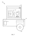
- FIG. 7 is a block diagram illustrating a design workstation used for circuit, layout, and logic design of a semiconductor component according to one configuration.
- Resonators can be used as oscillators or as components within a filter to achieve high order frequencies.
- Acoustically coupled resonators are resonators in which the electrical signals flowing through the resonator are transferred acoustically or electromechanically. Acoustically coupled resonators experience the problem of spurious responses. That is, signals at frequencies other than the resonant frequency appear in the frequency response of the resonator. This is particularly undesirable in a filter, where unwanted frequencies interfere with the filter's operation. If spurious responses continue to occur, the resonator operates in a spurious mode.
- the electrodes positioned on a piezoelectric core of a resonator are unbalanced to reduce spurious responses and to suppress the spurious mode.
- the widths of the electrodes on the piezoelectric core are adjusted to different sizes.
- the placement of electrodes on the piezoelectric core is adjusted.
- the resonator may have a first electrode.
- the resonator may also have a second electrode.
- the resonator has a first overhang distance between an outer edge of the first electrode and a first edge of a piezoelectric core.
- the resonator also has a second overhang distance between an outer edge of the second electrode and a second edge of the piezoelectric core.
- the first edge and the second edge may be opposing outer edges of the piezoelectric core.
- the electrodes are unbalanced by adjusting the first distance and the second distance to different values.
- the electrodes are unbalanced by placing an etched notch between at least two resonators in a multi-finger resonator configuration to introduce an acoustic boundary condition. If the number of fingers (e.g., electrodes) is large, then etched notches may be periodically placed between successive fingers (e.g., between every second and third finger or every fourth and fifth finger).
- FIG. 1 is a perspective view of a resonator 100 according to an aspect of the present disclosure.
- the resonator 100 includes a core 102 .
- the core 102 is made of piezoelectric materials such as Aluminum Nitride (AlN) and its alloys, such as those doped with Boron (B), Chromium (Cr), Erbium (Er) or Scandium (Sc); Zinc Oxide (ZnO); Lithium Niobate (LiNbO 3 ), Lithium Tantalate (LiTaO 3 ), Lead Zirconate Titanate or PZT (Pb[Zr x Ti 1-x ]O 3 0 ⁇ x ⁇ 1), Quartz (SiO 4 or SiO 2 ) crystals, and Topaz (Al 2 SiO 4 (F,OH) 2 ) crystals.
- the resonator core 102 may also be made of other like materials having a mechanical structure that can be stimulated in an electrical fashion through electromechanical coupling.
- the resonator 100 has a first electrode 104 and a second electrode 106 .
- the first electrode 104 and the second electrode 106 are made of materials including Molybdenum (Mo), Platinum (Pt), Copper (Cu), Aluminum (Al), Silver (Ag), Gold (Au), Tungsten (W), Nickel (Ni), or other like materials.
- a first signal 114 may be coupled to the first electrode 104
- a second signal 116 may be coupled to the second electrode 106 .
- the first signal 114 may be an electrical input signal and the second signal 116 may be an electrical output signal.
- the first electrode 104 and the second electrode 106 may be on any surface of the core 102 including opposing (not shown) or adjacent surfaces of the core 102 .
- the resonator 100 further includes a ground terminal 108 .
- the ground terminal 108 is coupled to a voltage ground or source supply voltage (Vss).
- Vss voltage ground or source supply voltage
- the ground terminal 108 may be separated into two or more separate ground terminals, which can be positioned on any surface of the core 102 .
- the first electrode 104 and/or the second electrode 106 and/or a first ground terminal can be positioned on a first surface of the core 102 , whereas the other of the first electrode 104 or the second electrode 106 , if any, and/or a second ground terminal are positioned on opposing or adjacent surfaces of the core 102 .
- the resonator 100 operates via a first electrical field 110 , a first mechanical displacement 112 , a second mechanical displacement 122 and a second electrical field 124 .
- the first mechanical displacement 112 and the second mechanical displacement 122 represent directions of mechanical displacement that occur within the resonator 100 when signals are present on the electrodes.
- the first electrical field 110 and the second electrical field 124 represent the direction of the electrical field through the resonator 100 .
- the first direction is expansion. That is, the first signal 114 is input into the first electrode 104 , which generates the first electrical field 110 , which is then in turn translated into the first mechanical displacement 112 that flows outward and expands a region of the core 102 .
- the second direction is contraction. That is, the second mechanical displacement 122 translates an inward, contracting mechanical displacement from a region of the core 102 into the second electrical field 124 , which flows into the second electrode 106 and becomes output as the second signal 116 .
- the transfer and translation of the electrical field to a mechanical displacement is due to the electromechanical coupling resonance caused by the piezoelectric effect.
- the expansion and contraction directions counteract each other in order to maintain constant parameters in the resonator 100 , such as a constant resonant frequency. Also, by changing the position of the electrodes on the core 102 , the parameters of the resonator 100 are modified and may become unbalanced.
- FIG. 2 is another perspective view of a resonator 200 according to an aspect of the present disclosure.
- the resonator 200 is similar to the resonator 100 in FIG. 1 , but can be made unbalanced by modifying a first electrode width 202 , a second electrode width 204 , a first overhang distance 206 and/or a second overhang distance 208 .
- a first pitch 118 , a second pitch 120 and an alternate pitch 126 may be modified. Modification of the first pitch 118 , the second pitch 120 and/or the alternate pitch 126 affects the resonant frequency as well as any spurious response resulting from the placement of the first electrode 104 and the second electrode 106 on the core 102 .
- the first overhang distance 206 is between an outer edge of the first electrode 104 and an outer edge of the core 102 that is substantially parallel to the outer edge of the first electrode 104 .
- the second overhang distance 208 is between an outer edge of the second electrode 106 and an outer edge of the core 102 that is substantially parallel to the outer edge of the second electrode 106 .
- the two opposing outer edges of the first electrode 104 forming the first electrode width 202 may be substantially parallel to each other.
- the two opposing outer edges of the second electrode 106 forming the second electrode width 204 may be substantially parallel to each other.
- the resonator 200 includes the adjustable parameters of the first pitch 118 , the second pitch 120 , and the alternate pitch 126 .
- each of the pitches may represent the distance between an outer edge of the core 102 to a mid-point of the core 102 .
- the mid-point of the core 102 may also be positioned in the very middle of two electrodes (e.g., the first electrode 104 and the second electrode 106 ).
- An electrode may also be positioned in the very middle of each of the pitches, as shown by the first electrode 104 in the middle of the first pitch 118 and the second electrode 106 in the middle of the second pitch 120 .
- the pitches may represent the distance between the center of one electrode (e.g., the first electrode 104 ) to the center of another electrode (e.g., the second electrode 106 ). This is shown by the alternate pitch 126 .
- the first pitch 118 and the second pitch 120 are the same. In another configuration, the first pitch 118 and the second pitch 120 are different.
- the first pitch 118 and the second pitch 120 determine the value of the resonant frequency or the fundamental resonance of the resonator 200 . For example, say that the value of both the first pitch 118 and the second pitch 120 is “W”.
- the wavelength corresponding to the overall frequency of the resonator 200 would be 2 W. Half this wavelength is W, which is the wavelength corresponding to the resonant frequency of the resonator 200 . Therefore, the resonant frequency of the resonator 100 can be calculated from knowing the value of the first pitch 118 and the second pitch 120 .
- the formula for calculating any frequency is to divide the speed of light by the relevant wavelength. In one configuration, the resonant frequency of the resonator 200 is around 700 MHz.
- the signal transmitted by the first electrode 104 leads to a spurious response occurring at a frequency that is approximately a quarter (1 ⁇ 4) of the frequency of the resonator 200 .
- the signal transmitted by the second electrode 106 also leads to another spurious response occurring at a frequency that is roughly 3 ⁇ 4 of the frequency of the resonator 200 .
- the overall frequency of a resonator is 1400 MHz, with a resonant frequency at 700 MHz (1 ⁇ 2 of 1400 MHz).
- a first undesired spurious response at approximately 350 MHz (1 ⁇ 4 of 1400 MHz) and a second undesired spurious response at approximately 1050 MHz (3 ⁇ 4 of 1400 MHz). Therefore, the position of the electrodes on the core 102 leads to the occurrence of different spurious responses at different frequencies.
- the edges of the core 102 in the resonator 200 experience the maximum mechanical displacement. For example, the edges would experience the most displacement in a positive “+x” linear direction.
- the very middle of the core 102 in the resonator 100 experiences the minimum mechanical displacement. For example, the middle would experience the lowest displacement, in a negative “ ⁇ x” linear direction.
- a more neutral mechanical displacement is experienced at a first region and a second region.
- the first region where the first electrode 104 may be positioned, is at the mid-point between one outer edge of the core 102 and the middle of the core 102 .
- the second region where the second electrode 106 may be positioned, is at the mid-point between another outer edge of the core 102 (not the outer edge of the first region) and the middle of the core 102 . Because the first region and the second region have a more neutral displacement, they also have the maximum electrical charge and the strongest electrical field.
- An electrode (such as the first electrode 104 or the second electrode 106 ) picks up a larger amount of charge generated in the first region and second region if placed there.
- an unbalanced resonator design decreases the presence of spurious responses at unwanted frequencies by reducing or even eliminating the spurious response and/or by moving the spurious frequency to a frequency that does not affect the resonator operation.
- the resonator 200 is unbalanced because modification of the above-described dimensions (e.g., the first electrode width 202 , the second electrode width 204 , the first overhang distance 206 and the second overhang distance 208 ) causes the first electrode 104 and the second electrode 106 to become asymmetrical, thereby also throwing off the balance and symmetry of the rest of the resonator 200 .
- This unbalancing allows the adjustment of resonator properties for suppressing spurious responses that occur at undesired frequencies.
- the strength of the spurious responses at undesired frequencies can be reduced by as much as 15 dB or more by adjusting the above-described dimensions (e.g., the first electrode width 202 , the second electrode width 204 , the first overhang distance 206 and the second overhang distance 208 ).
- the difference between the first electrode width 202 and the second electrode width 204 ranges from around 0.2 ⁇ m to around 0.4 ⁇ m.
- the difference between the first overhang distance 206 and the second overhang distance 208 ranges from around 0.2 ⁇ m to around 0.4 ⁇ m.
- the rejection/suppression of unwanted spurious response frequencies for a filter can be amplified in a cascade, multi-stage resonator configuration.
- a cascade, multi-stage resonator configuration spurious response frequencies are significantly attenuated, while some dominant frequencies survive, such as the resonant frequency.
- the cascade, multi-stage approach also suppresses the unwanted spurs (e.g., spurious frequency responses) without having to use external passive components, such as inductors and capacitors. This saves space as well as manufacturing costs.
- FIG. 3 is a perspective view of a multi-finger resonator 300 according to an aspect of the present disclosure.
- the multi-finger resonator 300 includes a first resonator 130 (that is identical to the resonator 100 in FIG. 1 ) on the left, and a second resonator 330 (that is also identical to the resonator 100 in FIG. 1 ) on the right.
- the fingers of the multi-finger resonator 300 are the four electrodes shown in FIG. 3 : a first electrode 104 , a second electrode 106 , a third electrode 304 and a fourth electrode 306 .
- adjusting the placement of the outermost electrodes—the first electrode 104 and the fourth electrode 306 — would control or suppress the largest spurious response(s) in the multi-finger resonator 300 .
- the configuration of the multi-finger resonator 300 may also be used to lower the collective electrical impedance of the overall device by having more fingers to match the resonator circuit to radio frequency (RF) environments having a particular resistance (e.g., 50 ⁇ ).
- RF radio frequency
- a core 132 , the first electrode 104 , the second electrode 106 , a ground terminal 108 , a first electrical field 110 , a first mechanical displacement 112 , a second mechanical displacement 122 , a second electrical field 124 , a first signal 114 and a second signal 116 may be identical to, respectively, a core 302 , the third electrode 304 , the fourth electrode 306 , a ground terminal 308 , a first electrical field 310 , a first mechanical displacement 312 , a second mechanical displacement 322 , a second electrical field 324 , a third signal 314 and a fourth signal 316 .
- the first signal 114 is the same as the third signal 314 and the second signal 116 is the same as the fourth signal 316 .
- the multi-finger resonator 300 shares a single ground terminal (not shown) instead of having the ground terminal 108 and the ground terminal 308 .
- the properties of the overall device would be modeled as one and a half (1.5) resonators.
- a half (0.5) resonator structure would be one electrode, and would have the frequency properties of one electrode as well.
- the placement of the electrodes would control or suppress any spurious responses. Adjusting the placement of the outermost electrodes would also control or suppress the largest spurious response(s).
- FIG. 4 is a side view of a multi-finger resonator 400 according to an aspect of the present disclosure.
- the multi-finger resonator 400 is similar to the multi-finger resonator 300 of FIG. 3 . In this configuration, the multi-finger resonator 400 has an etched notch 326 .
- the etched notch 326 can be placed between any two resonators in a multi-finger resonator structure to introduce an acoustic boundary condition.
- the etched notch 326 is placed between any two fingers or any two electrodes to also introduce an acoustic boundary.
- the acoustic boundary is a way to place an offset in the overall resonator circuit, which can alter periodicity or create additional asymmetry in the multi-finger resonator 400 . For example, if two resonators or two fingers are separated by an etched notch such as the etched notch 326 , then one resonator or one finger may be selectively stimulated while eliminating or reducing the frequency response from other resonators or fingers.
- certain resonating modes may be selectively stimulated while other harmonic modes may be suppressed, such as the spurious mode caused by unwanted spurious response frequencies.
- the resonant frequency of the overall resonator may also be tuned via selective placement of etched notches, such as the etched notch 326 .
- the etched notch 326 has a depth of 0.2 ⁇ m. Typical etching procedures such as dry plasma etching or wet chemical etching may be used to create the etched notch 326 .
- resonators are periodically attached in a multi-finger resonator structure, each resonator configured with unbalanced, asymmetrical electrode widths and overhang distances that can be continually adjusted. Such a multi-finger resonator structure is scalable to multiple, even-numbered finger amounts such as 2, 4, 6, 8, etc.
- the multi-finger resonator 400 of FIG. 4 also has dimensions that include a first electrode width 202 , a second electrode width 204 , a first overhang distance 206 and a second overhang distance 208 , which are similar to the same dimensions described for the resonator 200 of FIG. 2 .
- spurious mode suppression is disclosed.
- Resonators configured for spurious mode suppression can be implemented in filters that can support multiple pass bands of different communication standards. By suppressing spurious mode, unwanted frequencies are reduced.
- FIG. 5 is a process flow diagram illustrating a method 500 of making a resonator according to an aspect of the present disclosure.
- a piezoelectric core such as the core 102 in FIGS. 1-2 or the core 132 and the core 302 in FIGS. 3-4 .
- electrodes such as the first electrode 104 and the second electrode 106 in FIGS. 1-4 and/or the third electrode 304 and the fourth electrode 306 in FIGS. 3-4
- the set of electrodes are asymmetrically arranged by varying the electrode widths or the overhang distances in order to create an unbalanced resonator.
- at least one ground terminal (such as the ground terminal 108 in FIGS. 1-4 or the ground terminal 308 in FIGS. 3-4 ) is formed on the piezoelectric core.
- a bottom-to-top sequence is followed to form a resonator according to an aspect of the present disclosure.
- the at least one ground terminal is formed first.
- the piezoelectric core is formed on the at least one ground terminal. Electrodes are then arranged on the piezoelectric core. Finally, an etched notch is formed in the piezoelectric core.
- the ground terminal may be formed on any surface of the piezoelectric core.
- the electrodes include at least one input electrode and at least one output electrode.
- the input electrode and a ground terminal are on one surface of the piezoelectric core, and the output electrode and another ground terminal are on an opposite surface of the piezoelectric core.
- the input electrode and the output electrode are on one surface of the piezoelectric core, and the ground terminal is on an opposite surface of the piezoelectric core.
- the means for conducting electricity include the first electrode 104 , the second electrode 106 , the third electrode 304 and the fourth electrode 306 in FIGS. 1-4 .
- Other structures are also contemplated for the conducting means.
- the means for coupling to the ground includes the ground terminal 108 in FIGS. 1-2 and the ground terminal 108 and the ground terminal 308 in FIGS. 3-4 .
- FIG. 6 is a block diagram showing an exemplary wireless communication system 600 in which an aspect of the disclosure may be advantageously employed.
- FIG. 6 shows three remote units 620 , 630 , and 650 and two base stations 640 .
- Remote units 620 , 630 , and 650 include IC devices 625 A, 625 C, and 625 B that include the disclosed resonators. It will be recognized that other devices may also include the disclosed resonators, such as the base stations, switching devices, and network equipment.
- FIG. 6 shows forward link signals 680 from the base station 640 to the remote units 620 , 630 , and 650 and reverse link signals 690 from the remote units 620 , 630 , and 650 to base stations 640 .
- remote unit 620 is shown as a mobile telephone
- remote unit 630 is shown as a portable computer
- remote unit 650 is shown as a fixed location remote unit in a wireless local loop system.
- the remote units may be mobile phones, hand-held personal communication systems (PCS) units, portable data units such as personal data assistants, GPS enabled devices, navigation devices, set top boxes, music players, video players, entertainment units, fixed location data units such as meter reading equipment, or other devices that store or retrieve data or computer instructions, or combinations thereof.
- FIG. 6 illustrates remote units according to the aspects of the disclosure, the disclosure is not limited to these exemplary illustrated units. Aspects of the disclosure may be suitably employed in many devices, which include the disclosed resonators.
- FIG. 7 is a block diagram illustrating a design workstation used for circuit, layout, and logic design of a semiconductor component, such as the resonators disclosed above.
- a design workstation 700 includes a hard disk 701 containing operating system software, support files, and design software such as Cadence or OrCAD.
- the design workstation 700 also includes a display 702 to facilitate design of a circuit 710 or a semiconductor component 712 such as a resonator.
- a storage medium 704 is provided for tangibly storing the design of circuit 710 or the semiconductor component 712 .
- the design of the circuit 710 or the semiconductor component 712 may be stored on the storage medium 704 in a file format such as GDSII or GERBER.
- the storage medium 704 may be a CD-ROM, DVD, hard disk, flash memory, or other appropriate device.
- the design workstation 700 includes a drive apparatus 703 for accepting input from or writing output to the storage medium 704 .
- Data recorded on the storage medium 704 may specify logic circuit configurations, pattern data for photolithography masks, or mask pattern data for serial write tools such as electron beam lithography.
- the data may further include logic verification data such as timing diagrams or net circuits associated with logic simulations.
- Providing data on the storage medium 704 facilitates the design of the circuit 710 or the semiconductor component 712 by decreasing the number of processes for designing semiconductor wafers.
- the methodologies may be implemented with modules (e.g., procedures, functions, and so on) that perform the functions described herein.
- a machine-readable medium tangibly embodying instructions may be used in implementing the methodologies described herein.
- software codes may be stored in a memory and executed by a processor unit.
- Memory may be implemented within the processor unit or external to the processor unit.
- the term “memory” refers to types of long term, short term, volatile, nonvolatile, or other memory and is not to be limited to a particular type of memory or number of memories, or type of media upon which memory is stored.
- the functions may be stored as one or more instructions or code on a computer-readable medium. Examples include computer-readable media encoded with a data structure and computer-readable media encoded with a computer program.
- Computer-readable media includes physical computer storage media. A storage medium may be an available medium that can be accessed by a computer.
- such computer-readable media can include RAM, ROM, EEPROM, CD-ROM or other optical disk storage, magnetic disk storage or other magnetic storage devices, or other medium that can be used to store desired program code in the form of instructions or data structures and that can be accessed by a computer; disk and disc, as used herein, includes compact disc (CD), laser disc, optical disc, digital versatile disc (DVD), floppy disk and Blu-ray disc where disks usually reproduce data magnetically, while discs reproduce data optically with lasers. Combinations of the above should also be included within the scope of computer-readable media.
- instructions and/or data may be provided as signals on transmission media included in a communication apparatus.
- a communication apparatus may include a transceiver having signals indicative of instructions and data. The instructions and data are configured to cause one or more processors to implement the functions outlined in the claims.
Landscapes
- Physics & Mathematics (AREA)
- Acoustics & Sound (AREA)
- Chemical & Material Sciences (AREA)
- Crystallography & Structural Chemistry (AREA)
- Piezo-Electric Or Mechanical Vibrators, Or Delay Or Filter Circuits (AREA)
Priority Applications (5)
| Application Number | Priority Date | Filing Date | Title |
|---|---|---|---|
| US14/067,908 US9461614B2 (en) | 2013-10-30 | 2013-10-30 | Asymmetric unbalanced acoustically coupled resonators for spurious mode suppression |
| PCT/US2014/054034 WO2015065585A1 (en) | 2013-10-30 | 2014-09-04 | Asymmetric unbalanced acoustically coupled resonators for spurious mode suppression |
| CN201480059449.3A CN105684307B (zh) | 2013-10-30 | 2014-09-04 | 用于杂散模式抑制的非对称不平衡声耦合谐振器 |
| JP2016525027A JP2016539553A (ja) | 2013-10-30 | 2014-09-04 | スプリアスモード抑圧のための非対称不平衡音響結合共振器 |
| EP14766343.9A EP3063869A1 (en) | 2013-10-30 | 2014-09-04 | Asymmetric unbalanced acoustically coupled resonators for spurious mode suppression |
Applications Claiming Priority (1)
| Application Number | Priority Date | Filing Date | Title |
|---|---|---|---|
| US14/067,908 US9461614B2 (en) | 2013-10-30 | 2013-10-30 | Asymmetric unbalanced acoustically coupled resonators for spurious mode suppression |
Publications (2)
| Publication Number | Publication Date |
|---|---|
| US20150115777A1 US20150115777A1 (en) | 2015-04-30 |
| US9461614B2 true US9461614B2 (en) | 2016-10-04 |
Family
ID=51541372
Family Applications (1)
| Application Number | Title | Priority Date | Filing Date |
|---|---|---|---|
| US14/067,908 Expired - Fee Related US9461614B2 (en) | 2013-10-30 | 2013-10-30 | Asymmetric unbalanced acoustically coupled resonators for spurious mode suppression |
Country Status (5)
| Country | Link |
|---|---|
| US (1) | US9461614B2 (enExample) |
| EP (1) | EP3063869A1 (enExample) |
| JP (1) | JP2016539553A (enExample) |
| CN (1) | CN105684307B (enExample) |
| WO (1) | WO2015065585A1 (enExample) |
Families Citing this family (4)
| Publication number | Priority date | Publication date | Assignee | Title |
|---|---|---|---|---|
| US9379686B2 (en) * | 2014-03-04 | 2016-06-28 | Qualcomm Incorporated | Resonator with a staggered electrode configuration |
| US10476476B2 (en) * | 2016-12-15 | 2019-11-12 | Murata Manufacturing Co., Ltd. | MEMS resonator with suppressed spurious modes |
| US20190328360A1 (en) * | 2018-04-30 | 2019-10-31 | Vermon S.A. | Ultrasound transducer |
| US12483224B1 (en) * | 2021-07-16 | 2025-11-25 | Hrl Laboratories, Llc | Acoustically coupled dual resonators for phononic frequency comb generation |
Citations (14)
| Publication number | Priority date | Publication date | Assignee | Title |
|---|---|---|---|---|
| US3660699A (en) * | 1969-08-06 | 1972-05-02 | Denki Onkyo Co Ltd | Supporting means for piezoelectric transformers |
| US4329666A (en) | 1980-08-11 | 1982-05-11 | Motorola, Inc. | Two-pole monolithic crystal filter |
| US5424602A (en) * | 1991-02-12 | 1995-06-13 | Fujitsu Limited | Piezoelectric transformer showing a reduced input impedance and step-up/step-down operation for a wide range of load resistance |
| US6051915A (en) * | 1996-02-08 | 2000-04-18 | Tokin Corporation | Piezoelectric transformer |
| US6118209A (en) * | 1998-06-19 | 2000-09-12 | Matsushita Electric Industrial Co., Ltd. | Piezoelectric ceramic composition and piezoelectric transformer |
| US6192562B1 (en) | 1997-01-14 | 2001-02-27 | Murata Manufacturing Co., Ltd. | Method of producing piezoelectric component |
| US20020043900A1 (en) * | 2001-11-22 | 2002-04-18 | Samsung Electro-Mechanics Co., Ltd. | Piezoelectric transformer with patterns for recognizing node point |
| US6758199B2 (en) * | 2001-04-05 | 2004-07-06 | Mide Technology Corporation | Tuned power ignition system |
| US20040195937A1 (en) | 2003-04-01 | 2004-10-07 | Shogo Matsubara | Film bulk acoustic resonator and film bulk acoustic resonator circuit |
| US7414495B2 (en) | 2005-06-17 | 2008-08-19 | Matsushita Electric Industrial Co., Ltd. | Coupled FBAR filter |
| US20120050236A1 (en) | 2010-09-01 | 2012-03-01 | Qualcomm Mems Technologies, Inc. | Electromechanical systems piezoelectric contour mode differential resonators and filters |
| US20130021305A1 (en) | 2011-07-19 | 2013-01-24 | Qualcomm Mems Technologies, Inc. | Piezoelectric laterally vibrating resonator structure geometries for spurious frequency suppression |
| US20130134838A1 (en) | 2011-11-28 | 2013-05-30 | Qualcomm Mems Technologies, Inc. | Piezoelectric mems transformer |
| US20150256143A1 (en) * | 2014-03-04 | 2015-09-10 | Qualcomm Incorporated | Resonator with a staggered electrode configuration |
Family Cites Families (6)
| Publication number | Priority date | Publication date | Assignee | Title |
|---|---|---|---|---|
| JPS5327739U (enExample) * | 1976-08-18 | 1978-03-09 | ||
| JPS5873627U (ja) * | 1981-11-14 | 1983-05-18 | 日本特殊陶業株式会社 | 圧電濾波器 |
| JPH05327401A (ja) * | 1992-05-21 | 1993-12-10 | Murata Mfg Co Ltd | セラミックフィルタ |
| JP2000151354A (ja) * | 1998-11-13 | 2000-05-30 | Daishinku Corp | 圧電フィルタ |
| JP3835696B2 (ja) * | 2004-04-06 | 2006-10-18 | セイコーエプソン株式会社 | 発振回路および電子機器 |
| WO2007029280A1 (ja) * | 2005-03-28 | 2007-03-15 | Murata Manufacturing Co., Ltd. | 厚み縦圧電共振子 |
-
2013
- 2013-10-30 US US14/067,908 patent/US9461614B2/en not_active Expired - Fee Related
-
2014
- 2014-09-04 WO PCT/US2014/054034 patent/WO2015065585A1/en not_active Ceased
- 2014-09-04 EP EP14766343.9A patent/EP3063869A1/en not_active Withdrawn
- 2014-09-04 JP JP2016525027A patent/JP2016539553A/ja not_active Ceased
- 2014-09-04 CN CN201480059449.3A patent/CN105684307B/zh not_active Expired - Fee Related
Patent Citations (14)
| Publication number | Priority date | Publication date | Assignee | Title |
|---|---|---|---|---|
| US3660699A (en) * | 1969-08-06 | 1972-05-02 | Denki Onkyo Co Ltd | Supporting means for piezoelectric transformers |
| US4329666A (en) | 1980-08-11 | 1982-05-11 | Motorola, Inc. | Two-pole monolithic crystal filter |
| US5424602A (en) * | 1991-02-12 | 1995-06-13 | Fujitsu Limited | Piezoelectric transformer showing a reduced input impedance and step-up/step-down operation for a wide range of load resistance |
| US6051915A (en) * | 1996-02-08 | 2000-04-18 | Tokin Corporation | Piezoelectric transformer |
| US6192562B1 (en) | 1997-01-14 | 2001-02-27 | Murata Manufacturing Co., Ltd. | Method of producing piezoelectric component |
| US6118209A (en) * | 1998-06-19 | 2000-09-12 | Matsushita Electric Industrial Co., Ltd. | Piezoelectric ceramic composition and piezoelectric transformer |
| US6758199B2 (en) * | 2001-04-05 | 2004-07-06 | Mide Technology Corporation | Tuned power ignition system |
| US20020043900A1 (en) * | 2001-11-22 | 2002-04-18 | Samsung Electro-Mechanics Co., Ltd. | Piezoelectric transformer with patterns for recognizing node point |
| US20040195937A1 (en) | 2003-04-01 | 2004-10-07 | Shogo Matsubara | Film bulk acoustic resonator and film bulk acoustic resonator circuit |
| US7414495B2 (en) | 2005-06-17 | 2008-08-19 | Matsushita Electric Industrial Co., Ltd. | Coupled FBAR filter |
| US20120050236A1 (en) | 2010-09-01 | 2012-03-01 | Qualcomm Mems Technologies, Inc. | Electromechanical systems piezoelectric contour mode differential resonators and filters |
| US20130021305A1 (en) | 2011-07-19 | 2013-01-24 | Qualcomm Mems Technologies, Inc. | Piezoelectric laterally vibrating resonator structure geometries for spurious frequency suppression |
| US20130134838A1 (en) | 2011-11-28 | 2013-05-30 | Qualcomm Mems Technologies, Inc. | Piezoelectric mems transformer |
| US20150256143A1 (en) * | 2014-03-04 | 2015-09-10 | Qualcomm Incorporated | Resonator with a staggered electrode configuration |
Non-Patent Citations (3)
| Title |
|---|
| Abdolvand R., "Thin-Film Piezoelectric-On-Substrate Resonators and Narrowband Filters," 2008, 135 Pages. |
| Pulskamp J.S., et al., "Electrode-Shaping for the Excitation and Detection of Permitted Arbitrary Modes in Arbitrary Geometries in Piezoelectric Resonators," IEEE Transactions on Ultrasonics, Ferroelectrics, and Frequency Control, vol. 59 (5), May 2012, pp. 1043-1060. |
| Rosen D., et al., "Suppression of Spurious Lateral Modes in Thickness-Excited FBAR Resonators," Correspondence, IEEE transactions on Ultrasonics, ferroelectrics, and frequency control, vol. 52 (7), Jul. 2005, pp. 1189-1192. |
Also Published As
| Publication number | Publication date |
|---|---|
| EP3063869A1 (en) | 2016-09-07 |
| JP2016539553A (ja) | 2016-12-15 |
| WO2015065585A1 (en) | 2015-05-07 |
| US20150115777A1 (en) | 2015-04-30 |
| CN105684307A (zh) | 2016-06-15 |
| CN105684307B (zh) | 2018-10-09 |
Similar Documents
| Publication | Publication Date | Title |
|---|---|---|
| KR102166218B1 (ko) | 필터 | |
| CN110022135B (zh) | 可调谐谐振元件、滤波器电路和方法 | |
| JP6439799B2 (ja) | バンドパスフィルタおよびフィルタモジュール | |
| US10140406B2 (en) | Network synthesis design of microwave acoustic wave filters | |
| US8552818B2 (en) | Tunable filter | |
| US9038005B2 (en) | Network synthesis design of microwave acoustic wave filters | |
| US10727802B2 (en) | Method for producing a batch of acoustic wave filters | |
| JP6323348B2 (ja) | フィルタ装置 | |
| CN107592090B (zh) | 声波谐振器及其制造方法 | |
| US9130505B2 (en) | Multi-frequency reconfigurable voltage controlled oscillator (VCO) and method of providing same | |
| US10840884B2 (en) | Bulk acoustic wave (BAW) and passive-on-glass (POG) filter co-integration | |
| US9461614B2 (en) | Asymmetric unbalanced acoustically coupled resonators for spurious mode suppression | |
| CN108574473A (zh) | 共振器和用于提供共振器的方法 | |
| US9379686B2 (en) | Resonator with a staggered electrode configuration | |
| US8907747B2 (en) | Device using a filter with resonators | |
| US20190288662A1 (en) | Surface acoustic wave devices and method of fabricating the same | |
| US20130120082A1 (en) | Two-port resonators electrically coupled in parallel | |
| Chen et al. | Bulk Acoustic Wave Devices | |
| JP2006060871A (ja) | Sawフィルタパッケージ | |
| KR20140016533A (ko) | 박막 벌크 음향 필터 및 그 제조 방법 | |
| JP2006238496A (ja) | Sawフィルタパッケージ |
Legal Events
| Date | Code | Title | Description |
|---|---|---|---|
| AS | Assignment |
Owner name: QUALCOMM INCORPORATED, CALIFORNIA Free format text: ASSIGNMENT OF ASSIGNORS INTEREST;ASSIGNORS:YUN, CHANGHAN HOBIE;ZUO, CHENGJIE;VELEZ, MARIO FRANCISCO;AND OTHERS;REEL/FRAME:031597/0189 Effective date: 20131107 |
|
| STCF | Information on status: patent grant |
Free format text: PATENTED CASE |
|
| FEPP | Fee payment procedure |
Free format text: MAINTENANCE FEE REMINDER MAILED (ORIGINAL EVENT CODE: REM.); ENTITY STATUS OF PATENT OWNER: LARGE ENTITY |
|
| LAPS | Lapse for failure to pay maintenance fees |
Free format text: PATENT EXPIRED FOR FAILURE TO PAY MAINTENANCE FEES (ORIGINAL EVENT CODE: EXP.); ENTITY STATUS OF PATENT OWNER: LARGE ENTITY |
|
| STCH | Information on status: patent discontinuation |
Free format text: PATENT EXPIRED DUE TO NONPAYMENT OF MAINTENANCE FEES UNDER 37 CFR 1.362 |
|
| FP | Lapsed due to failure to pay maintenance fee |
Effective date: 20201004 |