US9431506B2 - Metal-oxide-semiconductor (MOS) transistor structure integrated with a resistance random access memory (RRAM) and the manufacturing methods thereof - Google Patents
Metal-oxide-semiconductor (MOS) transistor structure integrated with a resistance random access memory (RRAM) and the manufacturing methods thereof Download PDFInfo
- Publication number
- US9431506B2 US9431506B2 US14/702,228 US201514702228A US9431506B2 US 9431506 B2 US9431506 B2 US 9431506B2 US 201514702228 A US201514702228 A US 201514702228A US 9431506 B2 US9431506 B2 US 9431506B2
- Authority
- US
- United States
- Prior art keywords
- rram
- field effect
- effect transistor
- insulating film
- primary
- Prior art date
- Legal status (The legal status is an assumption and is not a legal conclusion. Google has not performed a legal analysis and makes no representation as to the accuracy of the status listed.)
- Active
Links
- 239000004065 semiconductor Substances 0.000 title claims abstract description 26
- 238000004519 manufacturing process Methods 0.000 title claims description 22
- 239000000758 substrate Substances 0.000 claims abstract description 34
- 238000000034 method Methods 0.000 claims abstract description 33
- 238000003860 storage Methods 0.000 claims abstract description 15
- 238000000231 atomic layer deposition Methods 0.000 claims abstract description 8
- 230000005669 field effect Effects 0.000 claims description 30
- 238000005530 etching Methods 0.000 claims description 13
- VYPSYNLAJGMNEJ-UHFFFAOYSA-N Silicium dioxide Chemical compound O=[Si]=O VYPSYNLAJGMNEJ-UHFFFAOYSA-N 0.000 claims description 10
- 229910021420 polycrystalline silicon Inorganic materials 0.000 claims description 10
- 229910052814 silicon oxide Inorganic materials 0.000 claims description 10
- 239000000463 material Substances 0.000 claims description 7
- 238000000151 deposition Methods 0.000 claims description 6
- 238000002955 isolation Methods 0.000 abstract description 8
- 238000009792 diffusion process Methods 0.000 abstract description 6
- 230000010354 integration Effects 0.000 abstract description 6
- QVGXLLKOCUKJST-UHFFFAOYSA-N atomic oxygen Chemical compound [O] QVGXLLKOCUKJST-UHFFFAOYSA-N 0.000 abstract description 4
- 230000015654 memory Effects 0.000 abstract description 4
- 229910052760 oxygen Inorganic materials 0.000 abstract description 4
- 239000001301 oxygen Substances 0.000 abstract description 4
- 238000005468 ion implantation Methods 0.000 abstract description 2
- 229910044991 metal oxide Inorganic materials 0.000 abstract 1
- 150000004706 metal oxides Chemical class 0.000 abstract 1
- 239000010410 layer Substances 0.000 description 58
- 229920002120 photoresistant polymer Polymers 0.000 description 30
- XUIMIQQOPSSXEZ-UHFFFAOYSA-N Silicon Chemical group [Si] XUIMIQQOPSSXEZ-UHFFFAOYSA-N 0.000 description 12
- 229910052710 silicon Inorganic materials 0.000 description 12
- 239000010703 silicon Substances 0.000 description 12
- 230000000873 masking effect Effects 0.000 description 10
- 229910052751 metal Inorganic materials 0.000 description 9
- 239000002184 metal Substances 0.000 description 9
- 229910052581 Si3N4 Inorganic materials 0.000 description 7
- HQVNEWCFYHHQES-UHFFFAOYSA-N silicon nitride Chemical compound N12[Si]34N5[Si]62N3[Si]51N64 HQVNEWCFYHHQES-UHFFFAOYSA-N 0.000 description 7
- 150000002500 ions Chemical class 0.000 description 5
- 238000002347 injection Methods 0.000 description 4
- 239000007924 injection Substances 0.000 description 4
- 230000000903 blocking effect Effects 0.000 description 3
- 238000002161 passivation Methods 0.000 description 3
- WFKWXMTUELFFGS-UHFFFAOYSA-N tungsten Chemical compound [W] WFKWXMTUELFFGS-UHFFFAOYSA-N 0.000 description 3
- 229910052721 tungsten Inorganic materials 0.000 description 3
- 239000010937 tungsten Substances 0.000 description 3
- RYGMFSIKBFXOCR-UHFFFAOYSA-N Copper Chemical compound [Cu] RYGMFSIKBFXOCR-UHFFFAOYSA-N 0.000 description 2
- 239000004020 conductor Substances 0.000 description 2
- 229910052802 copper Inorganic materials 0.000 description 2
- 239000010949 copper Substances 0.000 description 2
- 239000011229 interlayer Substances 0.000 description 2
- ATJFFYVFTNAWJD-UHFFFAOYSA-N Tin Chemical compound [Sn] ATJFFYVFTNAWJD-UHFFFAOYSA-N 0.000 description 1
- 239000012790 adhesive layer Substances 0.000 description 1
- 229910052782 aluminium Inorganic materials 0.000 description 1
- XAGFODPZIPBFFR-UHFFFAOYSA-N aluminium Chemical compound [Al] XAGFODPZIPBFFR-UHFFFAOYSA-N 0.000 description 1
- 230000000295 complement effect Effects 0.000 description 1
- 239000011521 glass Substances 0.000 description 1
- 239000012535 impurity Substances 0.000 description 1
- 239000012212 insulator Substances 0.000 description 1
- 238000001259 photo etching Methods 0.000 description 1
- 238000005498 polishing Methods 0.000 description 1
- 238000002360 preparation method Methods 0.000 description 1
- 239000000126 substance Substances 0.000 description 1
Images
Classifications
-
- H—ELECTRICITY
- H10—SEMICONDUCTOR DEVICES; ELECTRIC SOLID-STATE DEVICES NOT OTHERWISE PROVIDED FOR
- H10B—ELECTRONIC MEMORY DEVICES
- H10B63/00—Resistance change memory devices, e.g. resistive RAM [ReRAM] devices
- H10B63/30—Resistance change memory devices, e.g. resistive RAM [ReRAM] devices comprising selection components having three or more electrodes, e.g. transistors
-
- H—ELECTRICITY
- H01—ELECTRIC ELEMENTS
- H01L—SEMICONDUCTOR DEVICES NOT COVERED BY CLASS H10
- H01L29/00—Semiconductor devices adapted for rectifying, amplifying, oscillating or switching, or capacitors or resistors with at least one potential-jump barrier or surface barrier, e.g. PN junction depletion layer or carrier concentration layer; Details of semiconductor bodies or of electrodes thereof ; Multistep manufacturing processes therefor
- H01L29/40—Electrodes ; Multistep manufacturing processes therefor
- H01L29/43—Electrodes ; Multistep manufacturing processes therefor characterised by the materials of which they are formed
- H01L29/49—Metal-insulator-semiconductor electrodes, e.g. gates of MOSFET
- H01L29/51—Insulating materials associated therewith
-
- H—ELECTRICITY
- H01—ELECTRIC ELEMENTS
- H01L—SEMICONDUCTOR DEVICES NOT COVERED BY CLASS H10
- H01L21/00—Processes or apparatus adapted for the manufacture or treatment of semiconductor or solid state devices or of parts thereof
- H01L21/02—Manufacture or treatment of semiconductor devices or of parts thereof
- H01L21/04—Manufacture or treatment of semiconductor devices or of parts thereof the devices having at least one potential-jump barrier or surface barrier, e.g. PN junction, depletion layer or carrier concentration layer
- H01L21/18—Manufacture or treatment of semiconductor devices or of parts thereof the devices having at least one potential-jump barrier or surface barrier, e.g. PN junction, depletion layer or carrier concentration layer the devices having semiconductor bodies comprising elements of Group IV of the Periodic System or AIIIBV compounds with or without impurities, e.g. doping materials
- H01L21/28—Manufacture of electrodes on semiconductor bodies using processes or apparatus not provided for in groups H01L21/20 - H01L21/268
- H01L21/283—Deposition of conductive or insulating materials for electrodes conducting electric current
-
- H—ELECTRICITY
- H01—ELECTRIC ELEMENTS
- H01L—SEMICONDUCTOR DEVICES NOT COVERED BY CLASS H10
- H01L21/00—Processes or apparatus adapted for the manufacture or treatment of semiconductor or solid state devices or of parts thereof
- H01L21/02—Manufacture or treatment of semiconductor devices or of parts thereof
- H01L21/04—Manufacture or treatment of semiconductor devices or of parts thereof the devices having at least one potential-jump barrier or surface barrier, e.g. PN junction, depletion layer or carrier concentration layer
- H01L21/18—Manufacture or treatment of semiconductor devices or of parts thereof the devices having at least one potential-jump barrier or surface barrier, e.g. PN junction, depletion layer or carrier concentration layer the devices having semiconductor bodies comprising elements of Group IV of the Periodic System or AIIIBV compounds with or without impurities, e.g. doping materials
- H01L21/30—Treatment of semiconductor bodies using processes or apparatus not provided for in groups H01L21/20 - H01L21/26
- H01L21/302—Treatment of semiconductor bodies using processes or apparatus not provided for in groups H01L21/20 - H01L21/26 to change their surface-physical characteristics or shape, e.g. etching, polishing, cutting
- H01L21/306—Chemical or electrical treatment, e.g. electrolytic etching
- H01L21/30604—Chemical etching
-
- H01L27/2436—
-
- H—ELECTRICITY
- H01—ELECTRIC ELEMENTS
- H01L—SEMICONDUCTOR DEVICES NOT COVERED BY CLASS H10
- H01L29/00—Semiconductor devices adapted for rectifying, amplifying, oscillating or switching, or capacitors or resistors with at least one potential-jump barrier or surface barrier, e.g. PN junction depletion layer or carrier concentration layer; Details of semiconductor bodies or of electrodes thereof ; Multistep manufacturing processes therefor
- H01L29/66—Types of semiconductor device ; Multistep manufacturing processes therefor
- H01L29/66007—Multistep manufacturing processes
- H01L29/66075—Multistep manufacturing processes of devices having semiconductor bodies comprising group 14 or group 13/15 materials
- H01L29/66227—Multistep manufacturing processes of devices having semiconductor bodies comprising group 14 or group 13/15 materials the devices being controllable only by the electric current supplied or the electric potential applied, to an electrode which does not carry the current to be rectified, amplified or switched, e.g. three-terminal devices
- H01L29/66409—Unipolar field-effect transistors
- H01L29/66477—Unipolar field-effect transistors with an insulated gate, i.e. MISFET
-
- H01L45/1206—
-
- H01L45/16—
-
- H—ELECTRICITY
- H10—SEMICONDUCTOR DEVICES; ELECTRIC SOLID-STATE DEVICES NOT OTHERWISE PROVIDED FOR
- H10N—ELECTRIC SOLID-STATE DEVICES NOT OTHERWISE PROVIDED FOR
- H10N70/00—Solid-state devices without a potential-jump barrier or surface barrier, and specially adapted for rectifying, amplifying, oscillating or switching
- H10N70/011—Manufacture or treatment of multistable switching devices
-
- H—ELECTRICITY
- H10—SEMICONDUCTOR DEVICES; ELECTRIC SOLID-STATE DEVICES NOT OTHERWISE PROVIDED FOR
- H10N—ELECTRIC SOLID-STATE DEVICES NOT OTHERWISE PROVIDED FOR
- H10N70/00—Solid-state devices without a potential-jump barrier or surface barrier, and specially adapted for rectifying, amplifying, oscillating or switching
- H10N70/20—Multistable switching devices, e.g. memristors
- H10N70/253—Multistable switching devices, e.g. memristors having three or more terminals, e.g. transistor-like devices
-
- G—PHYSICS
- G11—INFORMATION STORAGE
- G11C—STATIC STORES
- G11C13/00—Digital stores characterised by the use of storage elements not covered by groups G11C11/00, G11C23/00, or G11C25/00
- G11C13/0002—Digital stores characterised by the use of storage elements not covered by groups G11C11/00, G11C23/00, or G11C25/00 using resistive RAM [RRAM] elements
-
- H01L45/04—
-
- H01L45/1226—
-
- H01L45/1233—
-
- H01L45/146—
-
- H01L45/1616—
-
- H—ELECTRICITY
- H10—SEMICONDUCTOR DEVICES; ELECTRIC SOLID-STATE DEVICES NOT OTHERWISE PROVIDED FOR
- H10N—ELECTRIC SOLID-STATE DEVICES NOT OTHERWISE PROVIDED FOR
- H10N70/00—Solid-state devices without a potential-jump barrier or surface barrier, and specially adapted for rectifying, amplifying, oscillating or switching
- H10N70/011—Manufacture or treatment of multistable switching devices
- H10N70/021—Formation of the switching material, e.g. layer deposition
- H10N70/023—Formation of the switching material, e.g. layer deposition by chemical vapor deposition, e.g. MOCVD, ALD
-
- H—ELECTRICITY
- H10—SEMICONDUCTOR DEVICES; ELECTRIC SOLID-STATE DEVICES NOT OTHERWISE PROVIDED FOR
- H10N—ELECTRIC SOLID-STATE DEVICES NOT OTHERWISE PROVIDED FOR
- H10N70/00—Solid-state devices without a potential-jump barrier or surface barrier, and specially adapted for rectifying, amplifying, oscillating or switching
- H10N70/20—Multistable switching devices, e.g. memristors
-
- H—ELECTRICITY
- H10—SEMICONDUCTOR DEVICES; ELECTRIC SOLID-STATE DEVICES NOT OTHERWISE PROVIDED FOR
- H10N—ELECTRIC SOLID-STATE DEVICES NOT OTHERWISE PROVIDED FOR
- H10N70/00—Solid-state devices without a potential-jump barrier or surface barrier, and specially adapted for rectifying, amplifying, oscillating or switching
- H10N70/801—Constructional details of multistable switching devices
- H10N70/821—Device geometry
- H10N70/823—Device geometry adapted for essentially horizontal current flow, e.g. bridge type devices
-
- H—ELECTRICITY
- H10—SEMICONDUCTOR DEVICES; ELECTRIC SOLID-STATE DEVICES NOT OTHERWISE PROVIDED FOR
- H10N—ELECTRIC SOLID-STATE DEVICES NOT OTHERWISE PROVIDED FOR
- H10N70/00—Solid-state devices without a potential-jump barrier or surface barrier, and specially adapted for rectifying, amplifying, oscillating or switching
- H10N70/801—Constructional details of multistable switching devices
- H10N70/821—Device geometry
- H10N70/826—Device geometry adapted for essentially vertical current flow, e.g. sandwich or pillar type devices
-
- H—ELECTRICITY
- H10—SEMICONDUCTOR DEVICES; ELECTRIC SOLID-STATE DEVICES NOT OTHERWISE PROVIDED FOR
- H10N—ELECTRIC SOLID-STATE DEVICES NOT OTHERWISE PROVIDED FOR
- H10N70/00—Solid-state devices without a potential-jump barrier or surface barrier, and specially adapted for rectifying, amplifying, oscillating or switching
- H10N70/801—Constructional details of multistable switching devices
- H10N70/881—Switching materials
- H10N70/883—Oxides or nitrides
- H10N70/8833—Binary metal oxides, e.g. TaOx
Definitions
- the present invention relates to a field effect transistor structure, in particular to a field effect transistor structure integrated with a RRAM and a manufacturing method thereof, belonging to the technical field of semiconductor memories.
- Information reading and writing of the RRAM is realized by reading or changing the resistance of the resistance-variable material.
- the resistance of the RRAM has a high state and a low state, which are represented by “0” and “1”. With different voltages, the resistance of the RRAM can be switched between the high state and the low state to realize information storage.
- the RRAM has advantages of simple preparation, high storage density, low operation voltage, quick speed of reading and writing, long service time, nondestructive access, low power, and in comparison with CMOS (complementary metal-oxide-semiconductor) high process compatibility, and therefore is regarded as one of the most powerful candidates of the next generation of “universal” memories.
- CMOS complementary metal-oxide-semiconductor
- MOS transistor structures metal-oxide-semiconductors, namely field effect transistors
- the RRAM is usually formed in the subsequent interconnection procedure of the MOS transistor.
- FIG. 1 The integration structure of the RRAM and the MOS transistor in the prior art can be seen in FIG.
- the MOS transistor structure comprises a source region 101 , a drain region 102 , a gate dielectric layer 103 , a gate electrode 104 , and an insulating layer 105 which isolates the gate region from other conductive layers of this unit;
- the metal interconnection structure comprises an interlayer isolating layer 106 in a primary layer interconnection, a diffusion blocking layer 107 and a copper interconnection line 108 in a contact hole, an etching blocking layer 109 and an interlayer isolating layer 110 in a second layer interconnection, and a diffusion blocking layer 111 and a copper interconnection line 112 in a contact hole of the second layer interconnection;
- the resistance random access structure comprises a resistance-variable material layer 113 and a conductive material layer 114 , and the insulating layer 115 isolates the RRAM from other conductor layers of this unit.
- the objective of the invention is to provide an integration structure of a RRAM and a MOS transistor to simplify the process of integrating the RRAM and the MOS transistor.
- the invention provides a MOS transistor structure integrated with a RRAM, comprising,
- a gate dielectric layer of said MOS transistor extends to the surface of a drain region of said MOS transistor
- the part of the gate dielectric layer on the surface of the drain region of the field effect transistor forms a resistance-variable storage layer of said RRAM.
- said semiconductor substrate is silicon or silicon on an insulator.
- the gate dielectric layer of said field effect transistor is made of a resistance-variable material with a high dielectric constant.
- the present invention also provides two methods for manufacturing the above-mentioned MOS transistor structure integrated with the RRAM.
- the first method for manufacturing the MOS transistor structure integrated with the RRAM comprises: forming a primary insulating film on the surface of the semiconductor substrate of the primary doping type; depositing a photoresist layer on said primary insulating film, and performing masking, exposure, and development to define positions of the source region and drain region of the MOS transistor; etching said primary insulating film at the positions of the source region and drain region of said MOS transistor to expose the semiconductor substrate; forming a source region and a drain region of a second doping type in said semiconductor substrate by ion injection or ion diffusion; stripping the photoresist; etching to remove the rest of the primary insulating film; growing a second insulating film on the surface of the semiconductor substrate by atomic layer deposition; depositing a primary conductive film on said second insulating film; depositing a photoresist on the surface of said primary conductive film and photo-etching to form patterns; and protecting the gate region of the MOS transistor with the photoresist; etching to remove
- said primary insulating film is made from silicon oxide.
- Said second insulating film is made from a resistance-variable material with a high dielectric constant.
- Said primary conductive film is made from n-type or p-type doped polycrystalline silicon.
- Said primary doping type is n-type, while said second doping type is p-type; or said primary doping type is p-type, and said second doping type is n-type.
- the second method for manufacturing the MOS transistor structure integrated with a RRAM comprises: forming a primary insulating film on the surface of a semiconductor substrate of a primary doping type; depositing a photoresist layer on said second insulating film, and performing masking, exposure, and development to define the position of the gate region; etching to remove said primary conductive film (which is not protected by the photoresist) and forming the gate electrode of the field effect transistor with the rest of the primary conductive film; stripping the photoresist; forming a source region and a drain region of a second doping type on both sides of said gate electrode in said semiconductor substrate respectively; etching to remove said primary insulating film above said source region and reserving said primary insulating film above said drain region, wherein said primary insulating film reserved above said drain region forms a resistance-variable storage layer of the RRAM.
- said primary insulating film is made from a resistance-variable material with a high dielectric constant.
- Said primary insulating film is made from silicon oxide.
- Said primary doping type is n-type, while said second doping type is p-type; or said primary doping type is p-type, and said second doping type is n-type.
- the high-quality gate dielectric layer of the MOS transistor and the resistance-variable storage layer of the RRAM are obtained by primary atomic layer deposition which integrates the RRAM and MOS transistor together without increasing steps.
- This process is simple and can combine the shallow trench isolation or field oxygen isolation and ion implantation or diffusion of source electrode and drain electrode to make integration convenient.
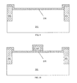
- FIG. 1 is a sectional view of a MOS transistor structure integrated with a RRAM in prior art.
- FIG. 2 is a sectional view of a MOS transistor structure integrated with a RRAM in one embodiment of the present invention.
- FIGS. 3-7 illustrate a workflow chart of a method for manufacturing a MOS transistor structure integrated with a RRAM in embodiment 1 of the present invention.
- FIGS. 8-12 illustrate a workflow chart of a method for manufacturing a MOS transistor structure integrated with a RRAM in embodiment 2 of the present invention.
- FIGS. 13-15 illustrate a part of the procedures in an integrated circuit composed of an n-type MOS transistor structure integrated with a RRAM.
- FIG. 2 illustrates a MOS transistor structure integrated with a RRAM in one embodiment of the present invention, which is a sectional view along the trench length direction of this unit.
- this unit is usually formed in a semiconductor substrate or a doped pit 20 .
- Said semiconductor substrate or doped pit is usually doped with n-type or p-type impurities at a low concentration.
- the doping type of the source region 21 and drain region 22 is opposite to that of the pit 20 .
- the source region 21 as the source electrode of the MOS transistor can be connected with an external electrode 31 directly or via a contact, and the gate electrode 25 of the MOS transistor can be connected with an external electrode 32 directly or via a contact.
- the gate dielectric layer 24 of the MOS transistor exceeds the gate electrode and extends above the drain region 22 , wherein the part 24 a of the gate dielectric layer extending to be above the drain region 22 forms the resistance-variable storage layer of the RRAM, and the resistance-variable storage layer 24 a is connected with an external electrode 33 directly or via a contact.
- the MOS transistor structure integrated with the RRAM disclosed in the present invention can be manufactured by many methods.
- FIGS. 3-7 illustrate a workflow chart of a method for manufacturing a MOS transistor structure integrated with a RRAM in embodiment 1 of the present invention.
- FIGS. 8-12 illustrate a workflow chart of a method for manufacturing a MOS transistor structure integrated with a RRAM in embodiment 2 of the present invention.
- FIGS. 13-15 depict a part of procedures in an integrated circuit composed of the n-type MOS transistor structure integrated with a RRAM.
- n-type doping is interchanged by p-type doping in the description below.
- a silicon substrate is taken as an example.
- STI shallow trench isolation
- FOS field oxygen isolation structure
- a photoresist layer 301 on the silicon oxide film 203 , and perform masking, exposure, and development to define the positions of the source region and drain region of the MOS transistor; etch to remove the exposed silicon oxide film 203 and expose the surface of the silicon substrate 201 ; and form the n-type source region 204 and the n-type drain region 205 of this unit in the silicon substrate 201 by ion injection, as shown in FIG. 4 .
- n-type or p-type doped polycrystalline silicon layer on the gate dielectric layer 206 , deposit a photoresist layer 302 on the polycrystalline silicon film, and perform masking, exposure, and development to form patterns; protect the gate region of the MOS transistor with the photoresist, and then etch to remove the exposed polycrystalline silicon film, wherein the rest of the polycrystalline silicon film forms the gate electrode 207 of the MOS transistor and the gate electrode 207 is located on the substrate between the source region 204 and the drain region 205 , as shown in FIG. 6 .
- the photoresist 302 cover the gate electrode 207 with an insulating film such as silicon nitride; deposit a photoresist layer; perform masking, exposure, and development to form patterns; etch to remove the exposed silicon nitride film, wherein the rest of the silicon nitride film forms the grid flank wall 208 of the MOS transistor.
- an insulating film such as silicon nitride
- strip the photoresist deposit a new photoresist layer on the above structure; mask, expose and develop to define the position of the source region 204 ; and etch to remove the part of the gate dielectric layer part above the source region 204 , wherein the part of the gate dielectric layer above the drain region 205 is reserved as the resistance-variable storage layer of the RRAM; stripping the photoresist to obtain a structure as shown in FIG. 7 .
- STI shallow trench isolation
- FET structure 202 field oxygen isolation structure
- n-type source region 204 and the n-type drain region 205 of the MOS transistor respectively on both sides of the gate electrode 207 in the silicon substrate 201 by ion injection or ion diffusion, as shown in FIG. 11 .
- the source region 204 and the drain region 205 of the MOS transistor are formed in a self-aligned manner.
- cover the gate electrode 207 deposit an insulating film such as silicon nitride; deposit a photoresist layer on the silicon nitride film; perform masking, exposure, and development to form patterns; etch to remove the silicon nitride film without protection of the photoresist, wherein the rest of the silicon nitride film forms the grid flank wall 208 of this unit; strip the photoresist; deposit a photoresist layer on the above structure and perform masking, exposure, and development to define the position of the source region 204 ; etch the part of the gate dielectric layer 206 above the source region 204 to expose the source region 204 , wherein the part of the gate dielectric layer 206 above the drain region 205 is reserved as the resistance-variable storage layer of the RRAM; strip the photoresist to obtain the structure as shown in FIG. 12 .
- an insulating film such as silicon nitride
- deposit a photoresist layer on the silicon nitride film perform masking, exposure,
- an interconnection metal layer can be further formed on the structures as shown in FIGS. 7 and 12 .
- a passivation layer 209 boron-phosphorosilicate glass for example
- an adhesive layer 210 such as TiN, is deposited in the contact hole first and then followed by the metal tungsten 211 , and this unit after chemical and mechanical polishing can be seen in FIG. 14 .
- a metal layer 212 such as aluminum on the above structure; deposit a photoresist layer on the metal layer 212 ; perform masking, exposure, and development to form patterns; etch to remove the exposed metal layer, form the source electrode, gate electrode and drain electrode with the rest of the metal layer; and strip the photoresist to obtain a structure as shown in FIG. 15 .
Landscapes
- Engineering & Computer Science (AREA)
- Microelectronics & Electronic Packaging (AREA)
- Power Engineering (AREA)
- Computer Hardware Design (AREA)
- Physics & Mathematics (AREA)
- Condensed Matter Physics & Semiconductors (AREA)
- General Physics & Mathematics (AREA)
- Manufacturing & Machinery (AREA)
- Ceramic Engineering (AREA)
- Chemical & Material Sciences (AREA)
- Chemical Kinetics & Catalysis (AREA)
- General Chemical & Material Sciences (AREA)
- Semiconductor Memories (AREA)
Abstract
Description
Claims (11)
Priority Applications (1)
Application Number | Priority Date | Filing Date | Title |
---|---|---|---|
US14/702,228 US9431506B2 (en) | 2012-06-21 | 2015-05-01 | Metal-oxide-semiconductor (MOS) transistor structure integrated with a resistance random access memory (RRAM) and the manufacturing methods thereof |
Applications Claiming Priority (8)
Application Number | Priority Date | Filing Date | Title |
---|---|---|---|
CN201210206510 | 2012-06-21 | ||
CN201210206312.9 | 2012-06-21 | ||
CN201210206510.5 | 2012-06-21 | ||
CN2012102063129A CN102709192A (en) | 2012-06-21 | 2012-06-21 | Manufacturing method of MOS (Metal Oxide Semiconductor) transistor structure integrated with resistive random access memory |
CN2012102065105A CN102709308A (en) | 2012-06-21 | 2012-06-21 | MOS (Metal Oxide Semiconductor) transistor structure integrated with resistive random access memory and manufacturing method of MOS transistor structure |
CN201210206312 | 2012-06-21 | ||
US13/663,077 US9054303B2 (en) | 2012-06-21 | 2012-10-29 | Metal-oxide-semiconductor (MOS) transistor structure integrated with a resistance random access memory (RRAM) and the manufacturing methods thereof |
US14/702,228 US9431506B2 (en) | 2012-06-21 | 2015-05-01 | Metal-oxide-semiconductor (MOS) transistor structure integrated with a resistance random access memory (RRAM) and the manufacturing methods thereof |
Related Parent Applications (1)
Application Number | Title | Priority Date | Filing Date |
---|---|---|---|
US13/663,077 Division US9054303B2 (en) | 2012-06-21 | 2012-10-29 | Metal-oxide-semiconductor (MOS) transistor structure integrated with a resistance random access memory (RRAM) and the manufacturing methods thereof |
Publications (2)
Publication Number | Publication Date |
---|---|
US20150311306A1 US20150311306A1 (en) | 2015-10-29 |
US9431506B2 true US9431506B2 (en) | 2016-08-30 |
Family
ID=49773688
Family Applications (2)
Application Number | Title | Priority Date | Filing Date |
---|---|---|---|
US13/663,077 Expired - Fee Related US9054303B2 (en) | 2012-06-21 | 2012-10-29 | Metal-oxide-semiconductor (MOS) transistor structure integrated with a resistance random access memory (RRAM) and the manufacturing methods thereof |
US14/702,228 Active US9431506B2 (en) | 2012-06-21 | 2015-05-01 | Metal-oxide-semiconductor (MOS) transistor structure integrated with a resistance random access memory (RRAM) and the manufacturing methods thereof |
Family Applications Before (1)
Application Number | Title | Priority Date | Filing Date |
---|---|---|---|
US13/663,077 Expired - Fee Related US9054303B2 (en) | 2012-06-21 | 2012-10-29 | Metal-oxide-semiconductor (MOS) transistor structure integrated with a resistance random access memory (RRAM) and the manufacturing methods thereof |
Country Status (1)
Country | Link |
---|---|
US (2) | US9054303B2 (en) |
Cited By (1)
Publication number | Priority date | Publication date | Assignee | Title |
---|---|---|---|---|
US11573957B2 (en) | 2019-12-09 | 2023-02-07 | Salesforce.Com, Inc. | Natural language processing engine for translating questions into executable database queries |
Families Citing this family (2)
Publication number | Priority date | Publication date | Assignee | Title |
---|---|---|---|---|
US9054303B2 (en) | 2012-06-21 | 2015-06-09 | Fudan University | Metal-oxide-semiconductor (MOS) transistor structure integrated with a resistance random access memory (RRAM) and the manufacturing methods thereof |
US20190010397A1 (en) * | 2017-07-06 | 2019-01-10 | Lam Research Ag | Liquid mixture and method for etching a substrate using the liquid mixture |
Citations (4)
Publication number | Priority date | Publication date | Assignee | Title |
---|---|---|---|---|
US20080186779A1 (en) * | 2007-02-02 | 2008-08-07 | Macronix International Co., Ltd. | Semiconductor device and memory and method of operating thereof |
US20110026297A1 (en) * | 2009-07-30 | 2011-02-03 | Art Talent Industrial Limited | Variable and reversible resistive element, non-volatile memory device and methods for operating and manufacturing the non-volatile memory device |
US20120020138A1 (en) * | 2010-07-20 | 2012-01-26 | Macronix International Co., Ltd. | Transistor having an adjustable gate resistance and semiconductor device comprising the same |
US20130341696A1 (en) | 2012-06-21 | 2013-12-26 | Fudan University | Metal-oxide-semiconductor (mos) transistor structure integrated with a resistance random access memory (rram) and the manufacturing methods thereof |
-
2012
- 2012-10-29 US US13/663,077 patent/US9054303B2/en not_active Expired - Fee Related
-
2015
- 2015-05-01 US US14/702,228 patent/US9431506B2/en active Active
Patent Citations (5)
Publication number | Priority date | Publication date | Assignee | Title |
---|---|---|---|---|
US20080186779A1 (en) * | 2007-02-02 | 2008-08-07 | Macronix International Co., Ltd. | Semiconductor device and memory and method of operating thereof |
US20110026297A1 (en) * | 2009-07-30 | 2011-02-03 | Art Talent Industrial Limited | Variable and reversible resistive element, non-volatile memory device and methods for operating and manufacturing the non-volatile memory device |
US20120020138A1 (en) * | 2010-07-20 | 2012-01-26 | Macronix International Co., Ltd. | Transistor having an adjustable gate resistance and semiconductor device comprising the same |
US20130341696A1 (en) | 2012-06-21 | 2013-12-26 | Fudan University | Metal-oxide-semiconductor (mos) transistor structure integrated with a resistance random access memory (rram) and the manufacturing methods thereof |
US9054303B2 (en) | 2012-06-21 | 2015-06-09 | Fudan University | Metal-oxide-semiconductor (MOS) transistor structure integrated with a resistance random access memory (RRAM) and the manufacturing methods thereof |
Non-Patent Citations (4)
Title |
---|
Final Office Action for U.S. Appl. No. 13/663,077 dated Aug. 15, 2014. |
Non-Final Office Action for U.S. Appl. No. 13/663,077 dated Dec. 2, 2013. |
Notice of Allowance for U.S. Appl. No. 13/663,077 dated Feb. 4, 2015. |
Restriction Requirement for U.S. Appl. No. 13/663,077 dated Sep. 11, 2013. |
Cited By (1)
Publication number | Priority date | Publication date | Assignee | Title |
---|---|---|---|---|
US11573957B2 (en) | 2019-12-09 | 2023-02-07 | Salesforce.Com, Inc. | Natural language processing engine for translating questions into executable database queries |
Also Published As
Publication number | Publication date |
---|---|
US20150311306A1 (en) | 2015-10-29 |
US9054303B2 (en) | 2015-06-09 |
US20130341696A1 (en) | 2013-12-26 |
Similar Documents
Publication | Publication Date | Title |
---|---|---|
US9748406B2 (en) | Semi-floating-gate device and its manufacturing method | |
JP5550286B2 (en) | Manufacturing method of semiconductor device | |
JP2000208766A (en) | Semiconductor device and its manufacture | |
US6962862B2 (en) | Manufacturing method of semiconductor device | |
US20090039408A1 (en) | Nonvolatile semiconductor memory and manufacturing method thereof | |
US20150318291A1 (en) | Semiconductor memory with u-shaped channel | |
JP2008244097A (en) | Semiconductor device and method of manufacturing the same | |
US9147835B2 (en) | Tunnel transistor structure integrated with a resistance random access memory (RRAM) and a manufacturing method thereof | |
US9431506B2 (en) | Metal-oxide-semiconductor (MOS) transistor structure integrated with a resistance random access memory (RRAM) and the manufacturing methods thereof | |
JP3195785B2 (en) | Semiconductor storage device and method of manufacturing the same | |
JP2012089772A (en) | Method of manufacturing semiconductor device | |
US9525020B2 (en) | Semiconductor device and method for forming the same | |
US8878253B2 (en) | Semiconductor devices | |
JP2004095745A (en) | Semiconductor device and method for manufacturing the same | |
CN102709192A (en) | Manufacturing method of MOS (Metal Oxide Semiconductor) transistor structure integrated with resistive random access memory | |
US20080277709A1 (en) | Dram structure | |
CN102709308A (en) | MOS (Metal Oxide Semiconductor) transistor structure integrated with resistive random access memory and manufacturing method of MOS transistor structure | |
US8129816B2 (en) | Semiconductor device and method of manufacturing the same | |
US7557012B2 (en) | Method for forming surface strap | |
TW201733021A (en) | Memory device, gate stack and method for manufacturing the same | |
US8362541B2 (en) | Manufacturing method of dynamic random access memory | |
JP2009164534A (en) | Semiconductor device and manufacturing method therefor | |
JP2008131023A (en) | Semiconductor device and its manufacturing method | |
US11855099B2 (en) | Metal-insulator-semiconductor tunnel diode memory | |
WO2022033164A1 (en) | Semiconductor structure and manufacturing method for semiconductor structure |
Legal Events
Date | Code | Title | Description |
---|---|---|---|
AS | Assignment |
Owner name: FUDAN UNIVERSITY, CHINA Free format text: ASSIGNMENT OF ASSIGNORS INTEREST;ASSIGNORS:LIN, XI;WANG, PENGFEI;SUN, QINGQING;AND OTHERS;REEL/FRAME:036092/0703 Effective date: 20150615 |
|
STCF | Information on status: patent grant |
Free format text: PATENTED CASE |
|
MAFP | Maintenance fee payment |
Free format text: PAYMENT OF MAINTENANCE FEE, 4TH YR, SMALL ENTITY (ORIGINAL EVENT CODE: M2551); ENTITY STATUS OF PATENT OWNER: SMALL ENTITY Year of fee payment: 4 |
|
FEPP | Fee payment procedure |
Free format text: MAINTENANCE FEE REMINDER MAILED (ORIGINAL EVENT CODE: REM.); ENTITY STATUS OF PATENT OWNER: SMALL ENTITY |