US9356426B2 - Electronic device, quantum interference device, atomic oscillator, electronic apparatus, and moving object - Google Patents
Electronic device, quantum interference device, atomic oscillator, electronic apparatus, and moving object Download PDFInfo
- Publication number
- US9356426B2 US9356426B2 US14/219,102 US201414219102A US9356426B2 US 9356426 B2 US9356426 B2 US 9356426B2 US 201414219102 A US201414219102 A US 201414219102A US 9356426 B2 US9356426 B2 US 9356426B2
- Authority
- US
- United States
- Prior art keywords
- package
- electronic component
- electronic
- section
- lid body
- Prior art date
- Legal status (The legal status is an assumption and is not a legal conclusion. Google has not performed a legal analysis and makes no representation as to the accuracy of the status listed.)
- Expired - Fee Related, expires
Links
- 230000005284 excitation Effects 0.000 claims description 29
- 229910052751 metal Inorganic materials 0.000 claims description 27
- 239000002184 metal Substances 0.000 claims description 27
- 150000001340 alkali metals Chemical group 0.000 claims description 24
- 238000001514 detection method Methods 0.000 claims description 14
- 230000008859 change Effects 0.000 claims description 2
- 239000007789 gas Substances 0.000 description 67
- 239000002585 base Substances 0.000 description 64
- 239000000463 material Substances 0.000 description 50
- 238000005304 joining Methods 0.000 description 23
- 238000000034 method Methods 0.000 description 22
- 229910052783 alkali metal Inorganic materials 0.000 description 21
- 239000007769 metal material Substances 0.000 description 21
- 238000003466 welding Methods 0.000 description 16
- 229920005989 resin Polymers 0.000 description 14
- 239000011347 resin Substances 0.000 description 14
- PXHVJJICTQNCMI-UHFFFAOYSA-N Nickel Chemical compound [Ni] PXHVJJICTQNCMI-UHFFFAOYSA-N 0.000 description 12
- 230000006870 function Effects 0.000 description 12
- PCHJSUWPFVWCPO-UHFFFAOYSA-N gold Chemical compound [Au] PCHJSUWPFVWCPO-UHFFFAOYSA-N 0.000 description 12
- 229910052737 gold Inorganic materials 0.000 description 12
- 239000010931 gold Substances 0.000 description 12
- 230000003287 optical effect Effects 0.000 description 12
- 230000009467 reduction Effects 0.000 description 12
- 239000000919 ceramic Substances 0.000 description 11
- 239000000470 constituent Substances 0.000 description 11
- 230000002265 prevention Effects 0.000 description 10
- 239000000956 alloy Substances 0.000 description 8
- 229910045601 alloy Inorganic materials 0.000 description 8
- 238000010586 diagram Methods 0.000 description 8
- RYGMFSIKBFXOCR-UHFFFAOYSA-N Copper Chemical compound [Cu] RYGMFSIKBFXOCR-UHFFFAOYSA-N 0.000 description 7
- BQCADISMDOOEFD-UHFFFAOYSA-N Silver Chemical compound [Ag] BQCADISMDOOEFD-UHFFFAOYSA-N 0.000 description 7
- 229910052802 copper Inorganic materials 0.000 description 7
- 239000010949 copper Substances 0.000 description 7
- 229910052709 silver Inorganic materials 0.000 description 7
- 239000004332 silver Substances 0.000 description 7
- VYZAMTAEIAYCRO-UHFFFAOYSA-N Chromium Chemical compound [Cr] VYZAMTAEIAYCRO-UHFFFAOYSA-N 0.000 description 6
- 229910052782 aluminium Inorganic materials 0.000 description 6
- XAGFODPZIPBFFR-UHFFFAOYSA-N aluminium Chemical compound [Al] XAGFODPZIPBFFR-UHFFFAOYSA-N 0.000 description 6
- 230000000694 effects Effects 0.000 description 6
- 229910052741 iridium Inorganic materials 0.000 description 6
- GKOZUEZYRPOHIO-UHFFFAOYSA-N iridium atom Chemical compound [Ir] GKOZUEZYRPOHIO-UHFFFAOYSA-N 0.000 description 6
- 229910052759 nickel Inorganic materials 0.000 description 6
- 230000010355 oscillation Effects 0.000 description 6
- 230000005855 radiation Effects 0.000 description 6
- 230000036544 posture Effects 0.000 description 5
- 239000000126 substance Substances 0.000 description 5
- XEEYBQQBJWHFJM-UHFFFAOYSA-N Iron Chemical compound [Fe] XEEYBQQBJWHFJM-UHFFFAOYSA-N 0.000 description 4
- 239000000853 adhesive Substances 0.000 description 4
- 230000001070 adhesive effect Effects 0.000 description 4
- 230000005281 excited state Effects 0.000 description 4
- 239000011261 inert gas Substances 0.000 description 4
- VYPSYNLAJGMNEJ-UHFFFAOYSA-N silicon dioxide Inorganic materials O=[Si]=O VYPSYNLAJGMNEJ-UHFFFAOYSA-N 0.000 description 4
- XOLBLPGZBRYERU-UHFFFAOYSA-N tin dioxide Chemical compound O=[Sn]=O XOLBLPGZBRYERU-UHFFFAOYSA-N 0.000 description 4
- 125000004429 atom Chemical group 0.000 description 3
- 238000005219 brazing Methods 0.000 description 3
- 229910052792 caesium Inorganic materials 0.000 description 3
- TVFDJXOCXUVLDH-UHFFFAOYSA-N caesium atom Chemical compound [Cs] TVFDJXOCXUVLDH-UHFFFAOYSA-N 0.000 description 3
- 238000010894 electron beam technology Methods 0.000 description 3
- 239000011521 glass Substances 0.000 description 3
- -1 polyethylene Polymers 0.000 description 3
- 229910052701 rubidium Inorganic materials 0.000 description 3
- IGLNJRXAVVLDKE-UHFFFAOYSA-N rubidium atom Chemical compound [Rb] IGLNJRXAVVLDKE-UHFFFAOYSA-N 0.000 description 3
- 229910000679 solder Inorganic materials 0.000 description 3
- 238000004544 sputter deposition Methods 0.000 description 3
- 238000007740 vapor deposition Methods 0.000 description 3
- 239000012808 vapor phase Substances 0.000 description 3
- DGAQECJNVWCQMB-PUAWFVPOSA-M Ilexoside XXIX Chemical compound C[C@@H]1CC[C@@]2(CC[C@@]3(C(=CC[C@H]4[C@]3(CC[C@@H]5[C@@]4(CC[C@@H](C5(C)C)OS(=O)(=O)[O-])C)C)[C@@H]2[C@]1(C)O)C)C(=O)O[C@H]6[C@@H]([C@H]([C@@H]([C@H](O6)CO)O)O)O.[Na+] DGAQECJNVWCQMB-PUAWFVPOSA-M 0.000 description 2
- KDLHZDBZIXYQEI-UHFFFAOYSA-N Palladium Chemical compound [Pd] KDLHZDBZIXYQEI-UHFFFAOYSA-N 0.000 description 2
- 239000004696 Poly ether ether ketone Substances 0.000 description 2
- PPBRXRYQALVLMV-UHFFFAOYSA-N Styrene Chemical compound C=CC1=CC=CC=C1 PPBRXRYQALVLMV-UHFFFAOYSA-N 0.000 description 2
- GWEVSGVZZGPLCZ-UHFFFAOYSA-N Titan oxide Chemical compound O=[Ti]=O GWEVSGVZZGPLCZ-UHFFFAOYSA-N 0.000 description 2
- RTAQQCXQSZGOHL-UHFFFAOYSA-N Titanium Chemical compound [Ti] RTAQQCXQSZGOHL-UHFFFAOYSA-N 0.000 description 2
- MCMNRKCIXSYSNV-UHFFFAOYSA-N Zirconium dioxide Chemical compound O=[Zr]=O MCMNRKCIXSYSNV-UHFFFAOYSA-N 0.000 description 2
- 229920000122 acrylonitrile butadiene styrene Polymers 0.000 description 2
- 230000009471 action Effects 0.000 description 2
- 238000005229 chemical vapour deposition Methods 0.000 description 2
- 229910017052 cobalt Inorganic materials 0.000 description 2
- 239000010941 cobalt Substances 0.000 description 2
- GUTLYIVDDKVIGB-UHFFFAOYSA-N cobalt atom Chemical compound [Co] GUTLYIVDDKVIGB-UHFFFAOYSA-N 0.000 description 2
- 238000002788 crimping Methods 0.000 description 2
- 230000007423 decrease Effects 0.000 description 2
- 239000005038 ethylene vinyl acetate Substances 0.000 description 2
- 229910052742 iron Inorganic materials 0.000 description 2
- 238000010030 laminating Methods 0.000 description 2
- BASFCYQUMIYNBI-UHFFFAOYSA-N platinum Chemical compound [Pt] BASFCYQUMIYNBI-UHFFFAOYSA-N 0.000 description 2
- 229920001200 poly(ethylene-vinyl acetate) Polymers 0.000 description 2
- 229920002530 polyetherether ketone Polymers 0.000 description 2
- 229920000139 polyethylene terephthalate Polymers 0.000 description 2
- 239000005020 polyethylene terephthalate Substances 0.000 description 2
- 229920000098 polyolefin Polymers 0.000 description 2
- 229920002635 polyurethane Polymers 0.000 description 2
- 239000004814 polyurethane Substances 0.000 description 2
- 239000010453 quartz Substances 0.000 description 2
- 238000002310 reflectometry Methods 0.000 description 2
- 229910052708 sodium Inorganic materials 0.000 description 2
- 239000011734 sodium Substances 0.000 description 2
- 239000010936 titanium Substances 0.000 description 2
- 229910052719 titanium Inorganic materials 0.000 description 2
- 239000004925 Acrylic resin Substances 0.000 description 1
- 229920000178 Acrylic resin Polymers 0.000 description 1
- 241000251468 Actinopterygii Species 0.000 description 1
- 229910052582 BN Inorganic materials 0.000 description 1
- PZNSFCLAULLKQX-UHFFFAOYSA-N Boron nitride Chemical compound N#B PZNSFCLAULLKQX-UHFFFAOYSA-N 0.000 description 1
- OKTJSMMVPCPJKN-UHFFFAOYSA-N Carbon Chemical compound [C] OKTJSMMVPCPJKN-UHFFFAOYSA-N 0.000 description 1
- BVKZGUZCCUSVTD-UHFFFAOYSA-L Carbonate Chemical compound [O-]C([O-])=O BVKZGUZCCUSVTD-UHFFFAOYSA-L 0.000 description 1
- 239000004709 Chlorinated polyethylene Substances 0.000 description 1
- 229920000877 Melamine resin Polymers 0.000 description 1
- 239000004640 Melamine resin Substances 0.000 description 1
- 229920008285 Poly(ether ketone) PEK Polymers 0.000 description 1
- 239000005062 Polybutadiene Substances 0.000 description 1
- 239000004698 Polyethylene Substances 0.000 description 1
- 239000004721 Polyphenylene oxide Substances 0.000 description 1
- 229910052581 Si3N4 Inorganic materials 0.000 description 1
- XUIMIQQOPSSXEZ-UHFFFAOYSA-N Silicon Chemical compound [Si] XUIMIQQOPSSXEZ-UHFFFAOYSA-N 0.000 description 1
- NRTOMJZYCJJWKI-UHFFFAOYSA-N Titanium nitride Chemical compound [Ti]#N NRTOMJZYCJJWKI-UHFFFAOYSA-N 0.000 description 1
- 229920001807 Urea-formaldehyde Polymers 0.000 description 1
- 238000010521 absorption reaction Methods 0.000 description 1
- XECAHXYUAAWDEL-UHFFFAOYSA-N acrylonitrile butadiene styrene Chemical compound C=CC=C.C=CC#N.C=CC1=CC=CC=C1 XECAHXYUAAWDEL-UHFFFAOYSA-N 0.000 description 1
- 239000004676 acrylonitrile butadiene styrene Substances 0.000 description 1
- 229920001893 acrylonitrile styrene Polymers 0.000 description 1
- PNEYBMLMFCGWSK-UHFFFAOYSA-N aluminium oxide Inorganic materials [O-2].[O-2].[O-2].[Al+3].[Al+3] PNEYBMLMFCGWSK-UHFFFAOYSA-N 0.000 description 1
- 229910002113 barium titanate Inorganic materials 0.000 description 1
- JRPBQTZRNDNNOP-UHFFFAOYSA-N barium titanate Chemical compound [Ba+2].[Ba+2].[O-][Ti]([O-])([O-])[O-] JRPBQTZRNDNNOP-UHFFFAOYSA-N 0.000 description 1
- 230000008901 benefit Effects 0.000 description 1
- 239000008280 blood Substances 0.000 description 1
- 210000004369 blood Anatomy 0.000 description 1
- 230000036772 blood pressure Effects 0.000 description 1
- 239000001506 calcium phosphate Substances 0.000 description 1
- 229910000389 calcium phosphate Inorganic materials 0.000 description 1
- 235000011010 calcium phosphates Nutrition 0.000 description 1
- 230000001413 cellular effect Effects 0.000 description 1
- 238000004891 communication Methods 0.000 description 1
- 230000001276 controlling effect Effects 0.000 description 1
- 229920001577 copolymer Polymers 0.000 description 1
- PMHQVHHXPFUNSP-UHFFFAOYSA-M copper(1+);methylsulfanylmethane;bromide Chemical compound Br[Cu].CSC PMHQVHHXPFUNSP-UHFFFAOYSA-M 0.000 description 1
- 239000013078 crystal Substances 0.000 description 1
- 230000006866 deterioration Effects 0.000 description 1
- 239000007772 electrode material Substances 0.000 description 1
- 239000003822 epoxy resin Substances 0.000 description 1
- 229920001973 fluoroelastomer Polymers 0.000 description 1
- 229910002804 graphite Inorganic materials 0.000 description 1
- 239000010439 graphite Substances 0.000 description 1
- 238000010438 heat treatment Methods 0.000 description 1
- AMGQUBHHOARCQH-UHFFFAOYSA-N indium;oxotin Chemical compound [In].[Sn]=O AMGQUBHHOARCQH-UHFFFAOYSA-N 0.000 description 1
- 238000009413 insulation Methods 0.000 description 1
- 230000031700 light absorption Effects 0.000 description 1
- 238000005259 measurement Methods 0.000 description 1
- 239000000203 mixture Substances 0.000 description 1
- 150000004767 nitrides Chemical class 0.000 description 1
- 229910052755 nonmetal Inorganic materials 0.000 description 1
- 230000003647 oxidation Effects 0.000 description 1
- 238000007254 oxidation reaction Methods 0.000 description 1
- 229910052574 oxide ceramic Inorganic materials 0.000 description 1
- 239000011224 oxide ceramic Substances 0.000 description 1
- 238000010422 painting Methods 0.000 description 1
- 229910052763 palladium Inorganic materials 0.000 description 1
- 239000005011 phenolic resin Substances 0.000 description 1
- 238000005268 plasma chemical vapour deposition Methods 0.000 description 1
- 238000007747 plating Methods 0.000 description 1
- 229910052697 platinum Inorganic materials 0.000 description 1
- 229920002647 polyamide Polymers 0.000 description 1
- 229920002857 polybutadiene Polymers 0.000 description 1
- 229920000647 polyepoxide Polymers 0.000 description 1
- 229920000728 polyester Polymers 0.000 description 1
- 229920000570 polyether Polymers 0.000 description 1
- 229920000573 polyethylene Polymers 0.000 description 1
- 229920001195 polyisoprene Polymers 0.000 description 1
- 229920000642 polymer Polymers 0.000 description 1
- 239000004800 polyvinyl chloride Substances 0.000 description 1
- 229920000915 polyvinyl chloride Polymers 0.000 description 1
- SCUZVMOVTVSBLE-UHFFFAOYSA-N prop-2-enenitrile;styrene Chemical compound C=CC#N.C=CC1=CC=CC=C1 SCUZVMOVTVSBLE-UHFFFAOYSA-N 0.000 description 1
- 230000001105 regulatory effect Effects 0.000 description 1
- 230000003014 reinforcing effect Effects 0.000 description 1
- 239000004065 semiconductor Substances 0.000 description 1
- 229910052710 silicon Inorganic materials 0.000 description 1
- 239000010703 silicon Substances 0.000 description 1
- 239000000377 silicon dioxide Substances 0.000 description 1
- HQVNEWCFYHHQES-UHFFFAOYSA-N silicon nitride Chemical compound N12[Si]34N5[Si]62N3[Si]51N64 HQVNEWCFYHHQES-UHFFFAOYSA-N 0.000 description 1
- 238000003980 solgel method Methods 0.000 description 1
- VEALVRVVWBQVSL-UHFFFAOYSA-N strontium titanate Chemical compound [Sr+2].[O-][Ti]([O-])=O VEALVRVVWBQVSL-UHFFFAOYSA-N 0.000 description 1
- 238000002230 thermal chemical vapour deposition Methods 0.000 description 1
- 229920002725 thermoplastic elastomer Polymers 0.000 description 1
- 238000002834 transmittance Methods 0.000 description 1
- QORWJWZARLRLPR-UHFFFAOYSA-H tricalcium bis(phosphate) Chemical compound [Ca+2].[Ca+2].[Ca+2].[O-]P([O-])([O-])=O.[O-]P([O-])([O-])=O QORWJWZARLRLPR-UHFFFAOYSA-H 0.000 description 1
- UONOETXJSWQNOL-UHFFFAOYSA-N tungsten carbide Chemical compound [W+]#[C-] UONOETXJSWQNOL-UHFFFAOYSA-N 0.000 description 1
- 229920006305 unsaturated polyester Polymers 0.000 description 1
- 238000001771 vacuum deposition Methods 0.000 description 1
- 239000002699 waste material Substances 0.000 description 1
- RUDFQVOCFDJEEF-UHFFFAOYSA-N yttrium(III) oxide Inorganic materials [O-2].[O-2].[O-2].[Y+3].[Y+3] RUDFQVOCFDJEEF-UHFFFAOYSA-N 0.000 description 1
- YVTHLONGBIQYBO-UHFFFAOYSA-N zinc indium(3+) oxygen(2-) Chemical compound [O--].[Zn++].[In+3] YVTHLONGBIQYBO-UHFFFAOYSA-N 0.000 description 1
- XLOMVQKBTHCTTD-UHFFFAOYSA-N zinc oxide Inorganic materials [Zn]=O XLOMVQKBTHCTTD-UHFFFAOYSA-N 0.000 description 1
- 239000011787 zinc oxide Substances 0.000 description 1
Images


Classifications
-
- H—ELECTRICITY
- H01—ELECTRIC ELEMENTS
- H01S—DEVICES USING THE PROCESS OF LIGHT AMPLIFICATION BY STIMULATED EMISSION OF RADIATION [LASER] TO AMPLIFY OR GENERATE LIGHT; DEVICES USING STIMULATED EMISSION OF ELECTROMAGNETIC RADIATION IN WAVE RANGES OTHER THAN OPTICAL
- H01S5/00—Semiconductor lasers
- H01S5/06—Arrangements for controlling the laser output parameters, e.g. by operating on the active medium
- H01S5/068—Stabilisation of laser output parameters
- H01S5/0683—Stabilisation of laser output parameters by monitoring the optical output parameters
- H01S5/0687—Stabilising the frequency of the laser
-
- G—PHYSICS
- G04—HOROLOGY
- G04F—TIME-INTERVAL MEASURING
- G04F5/00—Apparatus for producing preselected time intervals for use as timing standards
- G04F5/14—Apparatus for producing preselected time intervals for use as timing standards using atomic clocks
- G04F5/145—Apparatus for producing preselected time intervals for use as timing standards using atomic clocks using Coherent Population Trapping
-
- H—ELECTRICITY
- H03—ELECTRONIC CIRCUITRY
- H03B—GENERATION OF OSCILLATIONS, DIRECTLY OR BY FREQUENCY-CHANGING, BY CIRCUITS EMPLOYING ACTIVE ELEMENTS WHICH OPERATE IN A NON-SWITCHING MANNER; GENERATION OF NOISE BY SUCH CIRCUITS
- H03B17/00—Generation of oscillations using radiation source and detector, e.g. with interposed variable obturator
-
- H—ELECTRICITY
- H03—ELECTRONIC CIRCUITRY
- H03L—AUTOMATIC CONTROL, STARTING, SYNCHRONISATION OR STABILISATION OF GENERATORS OF ELECTRONIC OSCILLATIONS OR PULSES
- H03L1/00—Stabilisation of generator output against variations of physical values, e.g. power supply
- H03L1/02—Stabilisation of generator output against variations of physical values, e.g. power supply against variations of temperature only
- H03L1/04—Constructional details for maintaining temperature constant
-
- H—ELECTRICITY
- H03—ELECTRONIC CIRCUITRY
- H03L—AUTOMATIC CONTROL, STARTING, SYNCHRONISATION OR STABILISATION OF GENERATORS OF ELECTRONIC OSCILLATIONS OR PULSES
- H03L7/00—Automatic control of frequency or phase; Synchronisation
- H03L7/26—Automatic control of frequency or phase; Synchronisation using energy levels of molecules, atoms, or subatomic particles as a frequency reference
-
- H—ELECTRICITY
- H01—ELECTRIC ELEMENTS
- H01S—DEVICES USING THE PROCESS OF LIGHT AMPLIFICATION BY STIMULATED EMISSION OF RADIATION [LASER] TO AMPLIFY OR GENERATE LIGHT; DEVICES USING STIMULATED EMISSION OF ELECTROMAGNETIC RADIATION IN WAVE RANGES OTHER THAN OPTICAL
- H01S5/00—Semiconductor lasers
- H01S5/02—Structural details or components not essential to laser action
- H01S5/022—Mountings; Housings
- H01S5/02208—Mountings; Housings characterised by the shape of the housings
- H01S5/02212—Can-type, e.g. TO-CAN housings with emission along or parallel to symmetry axis
-
- H—ELECTRICITY
- H01—ELECTRIC ELEMENTS
- H01S—DEVICES USING THE PROCESS OF LIGHT AMPLIFICATION BY STIMULATED EMISSION OF RADIATION [LASER] TO AMPLIFY OR GENERATE LIGHT; DEVICES USING STIMULATED EMISSION OF ELECTROMAGNETIC RADIATION IN WAVE RANGES OTHER THAN OPTICAL
- H01S5/00—Semiconductor lasers
- H01S5/02—Structural details or components not essential to laser action
- H01S5/024—Arrangements for thermal management
- H01S5/02438—Characterized by cooling of elements other than the laser chip, e.g. an optical element being part of an external cavity or a collimating lens
- H01S5/02446—Cooling being separate from the laser chip cooling
-
- H—ELECTRICITY
- H01—ELECTRIC ELEMENTS
- H01S—DEVICES USING THE PROCESS OF LIGHT AMPLIFICATION BY STIMULATED EMISSION OF RADIATION [LASER] TO AMPLIFY OR GENERATE LIGHT; DEVICES USING STIMULATED EMISSION OF ELECTROMAGNETIC RADIATION IN WAVE RANGES OTHER THAN OPTICAL
- H01S5/00—Semiconductor lasers
- H01S5/10—Construction or shape of the optical resonator, e.g. extended or external cavity, coupled cavities, bent-guide, varying width, thickness or composition of the active region
- H01S5/18—Surface-emitting [SE] lasers, e.g. having both horizontal and vertical cavities
- H01S5/183—Surface-emitting [SE] lasers, e.g. having both horizontal and vertical cavities having only vertical cavities, e.g. vertical cavity surface-emitting lasers [VCSEL]
Definitions
- the present invention relates to an electronic device, a quantum interference device, an atomic oscillator, an electronic apparatus, and a moving object.
- an electronic device in which an electronic component subjected to temperature control is housed in a package, it is generally performed to evacuate the package for the purpose of preventing heat conduction from the outside of the package to the electronic component in the package.
- Patent Literature 1 JP-UM-A-57-155810
- a container (an electronic component) on the inner side, in which a crystal oscillation circuit, a heat generating element, and a thermosensitive element are housed is housed in another container (a package) on the outer side and a space between the containers is evacuated.
- Examples of the device in which the two electronic components subjected to temperature control at temperatures different from each other are housed in the package include an atomic oscillator that oscillates on the basis of energy transfer of atoms of alkali metal such as rubidium or cesium.
- a package houses a gas cell having alkali metal encapsulated therein together with a buffer gas, a light emitting section configured to emit excitation light for exciting the alkali metal in the gas cell, and a light detecting section configured to detect the excitation light transmitted through the gas cell. It is necessary to maintain the light emitting section and the gas cell at fixed temperatures different from each other in order to display a stable oscillation characteristic.
- An advantage of some aspects of the invention is to provide an electronic device that can suppress temperature fluctuation of each of two electronic components in a package while realizing a reduction in size, provide a quantum interference device and an atomic oscillator that can suppress temperature fluctuation of each of a light emitting section and a gas cell in a package while realizing a reduction in size, and further provide an electronic apparatus and a moving object including the atomic oscillator.
- An electronic device includes: a first electronic component and a second electronic component; and a package including an internal space in which the first electronic component and the second electronic component are housed to be separated from each other in a state in which the internal space is decompressed to pressure lower than the atmospheric pressure.
- the reflectance of at least a part of the outer surface of at least one electronic component of the first electronic component and the second electronic component to an electromagnetic wave having a wavelength of 4 ⁇ m is equal to or higher than 50%.
- the first electronic component and the second electronic component are arranged in the internal space of the package while being separated from each other.
- the internal space of the package has the pressure lower than the atmospheric pressure. Therefore, it is possible to suppress heat conduction and transfer of heat by convection between the package and the first and second electronic components and between the first electronic component and the second electronic component.
- heat radiated from the package is reflected on the outer surface of the first electronic component or the second electronic component. Therefore, even if a reduction in the size of the package is realized, it is possible to suppress transfer of heat from the outside of the package to the first electronic component or the second electronic component.
- Heat radiated from one electronic component of the first electronic component and the second electronic component is reflected on the other electronic component. Therefore, even if the distance between the first electronic component and the second electronic component is reduced, it is possible to suppress transfer of heat from the one electronic component to the other electronic component.
- the first electronic component is subjected to temperature control at a first temperature
- the second electronic component is subjected to temperature control at a second temperature higher than the first temperature
- the inner surface of the package includes a black or dark color portion.
- the reflectance of at least a part of the outer surface of the package to the electromagnetic wave having the wavelength of 4 ⁇ m is equal to or higher than 50%.
- the reflectance of at least a part of the outer surface of each of the first electronic component and the second electronic component to the electromagnetic wave having the wavelength of 4 ⁇ m is equal to or higher than 50%.
- a metal film is arranged on the outer surface of at least one electronic component of the first electronic component and the second electronic component.
- a quantum interference device includes the electronic device according to the application example described above, the first electronic component includes a light emitting section configured to emit light, and the second electronic component includes a gas cell having metal atoms excited by the light encapsulated therein.
- the quantum interference device it is possible to suppress temperature fluctuation of each of the light emitting section and the gas cell in the package while realizing a reduction in size.
- An atomic oscillator according to this application example includes the electronic device according to the application example described above.
- An electronic apparatus includes the electronic device according to the application example described above.
- the electronic apparatus has excellent reliability.
- a moving object according to this application example includes the electronic device according to the application example described above.
- the moving object has excellent reliability.
- FIG. 1 is a perspective view showing an atomic oscillator according to an embodiment of the invention.
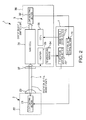
- FIG. 2 is a schematic diagram showing the schematic configuration of the atomic oscillator shown in FIG. 1 .
- FIG. 3 is a diagram for explaining an energy state of alkali metal in a gas cell included in the atomic oscillator shown in FIG. 1 .
- FIG. 4 is a graph showing, concerning a light emitting section and a light detecting section included in the atomic oscillator shown in FIG. 1 , a relation between a frequency difference between two lights emitted from the light emitting section and detection intensity in the light detecting section.
- FIG. 5 is a longitudinal sectional view of the atomic oscillator shown in FIG. 1 .
- FIG. 6 is a diagram for explaining the action of the atomic oscillator shown in FIG. 1 .
- FIG. 7 is a schematic diagram of a system configuration in which the atomic oscillator according to the embodiment of the invention is used in a positioning system that makes use of a GPS satellite.
- FIG. 8 is a perspective view showing the configuration of a moving object (an automobile) including the atomic oscillator according to the embodiment of the invention.
- Atomic Oscillator Quantum Interference Device
- the atomic oscillator according to the invention (the atomic oscillator including the quantum interference device according to the invention) is explained.
- the quantum interference device according to the invention is not limited to this.
- the quantum interference device according to the invention can also be applied to, for example, a magnetic sensor and a quantum memory besides the atomic oscillator.
- FIG. 1 is a perspective view showing an atomic oscillator according to an embodiment of the invention.
- FIG. 2 is a schematic diagram showing the schematic configuration of the atomic oscillator shown in FIG. 1 .
- FIG. 3 is a diagram for explaining an energy state of alkali metal in a gas cell included in the atomic oscillator shown in FIG. 1 .
- FIG. 4 is a graph showing, concerning a light emitting section and a light detecting section included in the atomic oscillator shown in FIG. 1 , a relation between a frequency difference between two lights emitted from the light emitting section and detection intensity in the light detecting section.
- FIG. 5 is a longitudinal sectional view of the atomic oscillator shown in FIG. 1 .
- FIG. 6 is a diagram for explaining the action of the atomic oscillator shown in FIG. 1 .
- an X axis, a Y axis, and a Z axis are shown as three axes orthogonal to one another.
- the distal end side of arrows of the axes shown in the figure is represented as “+ (plus)” and the proximal end side of the arrows is represented as “ ⁇ (minus)”.
- a direction parallel to the X axis is referred to as “X-axis direction”
- a direction parallel to the Y axis is referred to as “Y-axis direction”
- a direction parallel to the Z axis is referred to as “Z-axis direction”.
- the +Z-direction side (the upper side in FIG. 5 ) is referred to as “up” and the ⁇ Z-direction side (the lower side in FIG. 5 ) is referred to as “down”.
- An atomic oscillator 1 shown in FIG. 1 is an atomic oscillator that makes use of a quantum interference effect.
- the atomic oscillator 1 includes, as shown in FIG. 1 , a first unit 2 (a light emission side unit) functioning as a first electronic component, a second unit 3 (a light detection side unit) functioning as a second electronic component, a package 5 configured to house the foregoing, a wiring board 6 (a board) configured to support the package 5 , and a control section 7 mounted on the wiring board 6 .
- the first unit 2 includes, as shown in FIGS. 1 and 2 , a light emitting section 21 and a first package 22 (a light emission side package) configured to house the light emitting section 21 .
- the second unit 3 includes a gas cell 31 , a light detecting section 32 , a heater 33 , a temperature sensor 34 , a coil 35 , and a second package 36 (a light detection side package) configured to house the foregoing.
- the first unit 2 and the second unit 3 are electrically connected to the control section 7 via a wire (not shown in the figure) of the wiring board 6 and controlled to be driven by the control section 7 .
- alkali metal such as gaseous rubidium, cesium, or sodium is encapsulated in the gas cell 31 .
- the alkali metal has energy levels of a three level system and can take three states, i.e., two base states (base states 1 and 2) having different energy levels and an excited state.
- the base state 1 is an energy state lower than the base state 2.
- the light emitting section 21 emits the two kinds of lights (the resonance light 1 and the resonance light 2) having the different frequencies to the gas cell 31 .
- the light emitting section 21 fixes the frequency ⁇ 1 of the resonance light 1 and changes the frequency ⁇ 2 of the resonance light 2. Then, when the difference ( ⁇ 1 ⁇ 2) between the frequency ⁇ 1 of the resonance light 1 and the frequency ⁇ 2 of the resonance light 2 coincides with a frequency ⁇ 0 equivalent to the energy difference between the base state 1 and the base state 2, the detection intensity of the light detecting section 32 steeply rises as shown in FIG. 4 .
- the light detecting section 32 detects a signal of such a steep rise as an EIT signal.
- the EIT signal has an eigenvalue determined by a type of the alkali metal. Therefore, it is possible to realize a highly accurate oscillator by using such an EIT signal as a reference.
- the first unit 2 (the first electronic component) includes the light emitting section 21 and the first package 22 configured to house the light emitting section 21 .
- the light emitting section 21 has a function of emitting excitation light for exciting alkali metal atoms in the gas cell 31 .
- the light emitting section 21 emits two kinds of lights (the resonance light 1 and the resonance light 2) having the different frequencies.
- the frequency ⁇ 1 of the resonance light 1 can excite the alkali metal in the gas cell 31 from the base state 1 to the excited state.
- the frequency ⁇ 2 of the resonance light 2 can excite the alkali metal in the gas cell 31 from the base state 2 to the excited state.
- the light emitting section 21 is not particularly limited as long as the light emitting section 21 can emit the excitation light.
- a semiconductor laser such as a vertical cavity surface emitting laser (VCSEL) can be used.
- VCSEL vertical cavity surface emitting laser
- the light emitting section 21 is subjected to temperature control to temperature (a first temperature) different from the temperature of the gas cell 31 , for example, about 30° C. by a not-shown temperature control element (a heat generating resistor, a Peltier element, etc.).
- a first temperature different from the temperature of the gas cell 31 , for example, about 30° C.
- a not-shown temperature control element a heat generating resistor, a Peltier element, etc.
- the first package 22 houses the light emitting section 21 .
- the first package 22 includes, as shown in FIG. 5 , a base 221 (a light emission side base) and a lid body 222 (a light emission side lid body).
- the base 221 directly or indirectly supports the light emitting section 21 .
- the base 221 is formed in a tabular shape and formed in a circular shape in plan view.
- the light emitting section 21 (a mounted component) is set (mounted) on one surface (a mounting surface) of the base 221 .
- a plurality of terminals 223 (leads) project in the ⁇ X-axis direction.
- the plurality of terminals 223 are electrically connected to the light emitting section 21 via a not-shown wire.
- the plurality of terminals 223 extend in the X-axis direction and are arranged in one direction (in this embodiment, the Y-axis direction) to be parallel to one another.
- a constituent material of the base 221 is not particularly limited.
- a ceramics material, a metal material, a resin material, and the like can be used.
- the lid body 222 which covers the light emitting section 21 on the base 221 , is joined to the base 221 .
- the lid body 222 is formed in a bottomed tubular shape opening at one end.
- a tubular portion of the lid body 222 is formed in a cylindrical shape.
- the opening at one end of the lid body 222 is closed by the base 221 .
- a window section 23 is provided at the other end of the lid body 222 , that is, a bottom section on the opposite side of the opening of the lid body 222 .
- the window section 23 is provided on an optical axis “a” between the gas cell 31 and the light emitting section 21 .
- the window section 23 has transparency to the excitation light.
- the window section 23 is configured by a lens. Consequently, it is possible to irradiate excitation light LL on the gas cell 31 without waste.
- the window section 23 has a function of changing the excitation light LL to parallel light. Consequently, it is possible to simply and surely prevent the excitation light LL from being reflected on the inner wall of the gas cell 31 . Therefore, it is possible to suitably cause resonance of the excitation light in the gas cell 31 and, as a result, improve an oscillation characteristic of the atomic oscillator 1 .
- the window section 23 is not limited to the lens and may be an optical component other than the lens such as a polarizing plate, a ⁇ /4 wave plate, or a dimmer filter or may be a tabular member having simple optical transparency as long as the optical component has transparency to the excitation light.
- the optical components only have to be provided between the light emitting section 21 and the gas cell 31 .
- the optical components may be provided between a window section 37 and the light emitting section 21 or may be provided between the first package 22 and the second package 36 .
- the reflectance of the outer surface (a portion excluding the window section 23 ) of the lid body 222 to an electromagnetic wave having a wavelength of 4 ⁇ m (i.e., a far-infrared ray) is equal to or higher than 50%. Consequently, heat radiated from the package 5 is reflected on the outer surface of the lid body 222 (the outer surface of the first electronic component). Therefore, even if a reduction in the size of the package 5 is realized, it is possible to suppress transfer of heat from the outside of the package 5 to the lid body 222 .
- Heat radiated from the second unit 3 is reflected on the outer surface of the lid body 222 . Therefore, even if the distance between the first unit 2 and the second unit 3 is reduced, it is possible to suppress transfer of heat from the second unit 3 to the first unit 2 .
- the reflectance of the outer surface of the lid body 222 to the electromagnetic wave having the wavelength of 4 ⁇ m (hereinafter also referred to as “heat reflectance”) is higher. Therefore, the reflectance is preferably equal to or higher than 75%, more preferably equal to or higher than 90%, and most preferably equal to or higher than 95%.
- a constituent material of a portion other than the window section 23 of the lid body 222 is not particularly limited.
- a ceramics material, a metal material, and a resin material can be used.
- the metal material is preferably used. Consequently, it is possible to set the heat reflectance of the outer surface of the lid body 222 to be equal to or higher than 75%.
- the base 221 is formed of the metal material, the base 221 and the lid body 222 can be relatively easily and surely hermetically joined by welding.
- the metal material forming the lid body 222 is not particularly limited.
- metal such as copper (heat reflectance is 97.93%), silver (heat reflectance is 98.47%), gold (heat reflectance is 98.62%), titanium (heat reflectance is 78.04%), chrome (heat reflectance is 93.77%), iron (heat reflectance is 87.09%), cobalt (heat reflectance is 87.75%), nickel (heat reflectance is 92.38%), aluminum (heat reflectance is 99.03%), iridium (heat reflectance is 98.73%), and lead (heat reflectance is 98.90%) or an alloy including at least one of these kinds of metal can be used.
- copper, silver, gold, chrome, nickel, aluminum, iridium, or lead is preferably used. From the viewpoint of excellent chemical stability, gold is preferably used.
- the lid body 222 may be formed of one kind of metal or alloy or may be formed by laminating two or more kinds of metal or alloys.
- a metal film is preferably provided on the outer surface of the lid body 222 . Consequently, even if the heat reflectance of a base material of the lid body 222 is not high, it is possible to set the reflectance of a part where the metal film is provided to the electromagnetic wave having the wavelength of 4 ⁇ m to be equal to or higher than 75%. Further, it is possible to improve the heat reflectance of the lid body 222 while using, for the base material of the lid body 222 , a material suitable for joining with the base 221 and excellent in mechanical strength.
- metal film As a material used for the metal film, among the metal materials explained above, from the viewpoint of high heat reflectance, copper, silver, gold, chrome, nickel, aluminum, iridium, or lead is preferably used. From the view point of excellent chemical stability, gold is preferably used.
- a method of forming the metal film is not particularly limited.
- vapor phase film forming methods such as vapor deposition and sputtering can be used.
- the metal film only has to be provided in a part where heat radiated from the second unit 3 or the package 5 reaches.
- the metal film does not always have to be provided in the entire region of the outer surface of the lid body 222 .
- the portion other than the window section 23 of the lid body 222 and the window section 23 can be integrally formed.
- the portion other than the window section 23 of the lid body 222 is formed of a material not having transparency to the excitation light
- the portion other than the window section 23 of the lid body 222 and the window section 23 only have to be formed of separate bodies and joined by a publicly-known joining method.
- the base 221 and the lid body 222 are preferably hermetically jointed. That is, the inside of the first package 22 is preferably an airtight space. Consequently, it is possible to set the inside of the first package 22 in a decompressed state (a state in which the inside of the first package 22 is decompressed to pressure lower than the atmospheric pressure) or an inert gas encapsulated state. As a result, it is possible to improve characteristics of the atomic oscillator 1 .
- a method of joining the base 221 and the lid body 222 is not particularly limited.
- brazing seam welding, energy beam welding (laser welding, electron beam welding, etc.), and the like can be used.
- a joining member for joining the base 221 and the lid body 222 may be interposed between the base 221 and the lid body 222 .
- a component other than the light emitting section 21 may be housed in the first package 22 .
- a temperature control element configured to control the temperature of the light emitting section 21 , a temperature sensor, or the like may be housed in the first package 22 .
- the temperature control element include a heat generating resistor (a heater) and a Peltier element.
- the first package 22 including the base 221 and the lid body 222 , it is possible to house the light emitting section 21 in the first package 22 while allowing emission of the excitation light from the light emitting section 21 to the outside of the first package 22 .
- the first package 22 is held by the package 5 such that the base 221 is arranged on the opposite side of the second package 36 .
- the second unit 3 (the second electronic component) includes the gas cell 31 , the light detecting section 32 , the heater 33 , the temperature sensor 34 , the coil 35 , and the second package 36 configured to house the foregoing.
- Gaseous alkali metal such as rubidium, cesium, or sodium is encapsulated in the gas cell 31 .
- the gas cell 31 includes, although not-shown in the figure, a main body section including a columnar through-hole and a pair of window sections configured to close both openings of the through-hole. Consequently, an internal space for encapsulating the alkali metal is formed.
- the window sections of the gas cell 31 have transparency to the excitation light emitted from the light emitting section 21 .
- the excitation light made incident in the gas cell 31 is transmitted through one window section.
- the excitation light emitted from the gas cell 31 is transmitted through the other window section.
- a material forming the window sections of the gas cell 31 is not particularly limited as long as the material has transparency to the excitation light.
- the material include a glass material and quartz.
- a material forming the main body section of the gas cell 31 is not particularly limited and may be a metal material, a resin material, or the like or, like the window sections, may be a glass material, quartz, or the like.
- the window sections are hermetically joined to the main body section. Consequently, it is possible to form the internal space of the gas cell 31 as an airtight space.
- a method of joining the main body section and the window sections of the gas cell 31 is determined according to the constituent materials and is not particularly limited. For example, a joining method by an adhesive, a direct joining method, and an anode joining method can be used.
- the gas cell 31 is subjected to temperature control to temperature (a second temperature) different from the temperature of the light emitting section 21 , for example, about 70° C. by the heater 33 .
- the second unit 3 is subjected to temperature control at temperature higher than the temperature of the first unit 2 .
- a problem due to transfer of heat by radiation between the package 5 and the first and second units 2 and 3 and between the first unit 2 and the second unit 3 becomes conspicuous. Therefore, in this case, an effect by the application of the invention conspicuously appears.
- the light detecting section 32 has a function of detecting intensity of the excitation light LL (the resonance lights 1 and 2) transmitted through the gas cell 31 .
- the light detecting section 32 is not particularly limited as long as the light detecting section 32 can detect the excitation light.
- photodetectors such as a solar cell and a photodiode can be used.
- the heater 33 has a function of heating the gas cell 31 (more specifically, the alkali metal in the gas cell 31 ). Consequently, it is possible to maintain the alkali metal in the gas cell 31 gaseous.
- the heater 33 generates heat through energization.
- the heater 33 is configured by, for example, a heat generating resistor provided on the outer surface of the gas cell 31 .
- the heat generating resistor is formed using, for example, a chemical vapor deposition method (CVD) such as a plasma CVD or a thermal CVD, a dry plating method such as vacuum deposition, or a sol-gel method.
- CVD chemical vapor deposition method
- a plasma CVD or a thermal CVD a dry plating method such as vacuum deposition
- sol-gel method sol-gel method
- the heat generating resistor is formed of a material having transparency to the excitation light, specifically, for example, a transparent electrode material such as an oxide such as ITO (Indium Tin Oxide), IZO (Indium Zinc Oxide), In 3 O 3 , SnO 2 , SnO 2 containing Sb, or ZnO containing Al.
- a transparent electrode material such as an oxide such as ITO (Indium Tin Oxide), IZO (Indium Zinc Oxide), In 3 O 3 , SnO 2 , SnO 2 containing Sb, or ZnO containing Al.
- the heater 33 is not particularly limited as long as the heater 33 can heat the gas cell 31 and may be in non-contact with the gas cell 31 .
- a Peltier element may be used instead of the heater 33 or together with the heater 33 to heat the gas cell 31 .
- the heater 33 is electrically connected to a below-mentioned temperature control section 72 of the control section 7 and energized.
- the temperature sensor 34 detects the temperature of the heater 33 or the gas cell 31 .
- a heat value of the heater 33 is controlled on the basis of a detection result of the temperature sensor 34 . Consequently, it is possible to maintain the alkali metal atoms in the gas cell 31 at a desired temperature.
- a setting position of the temperature sensor 34 is not particularly limited and may be, for example, on the heater 33 or on the outer surface of the gas cell 31 .
- the temperature sensor 34 is not particularly limited. Various temperature sensors such as a thermistor and a thermocouple can be used.
- the temperature sensor 34 is electrically connected to the temperature control section 72 of the control section 7 , which will be described later, via a not-shown wire.
- the coil 35 has a function of generating a magnetic field through energization. Consequently, by applying the magnetic field to the alkali metal in the gas cell 31 , it is possible to expand, through Zeeman splitting, a gap between energy levels in which the alkali metal is degenerated and improve resolution. As a result, it is possible to improve accuracy of an oscillation frequency of the atomic oscillator 1 .
- the magnetic field generated by the coil 35 may be a direct-current magnetic field or an alternating-current magnetic field or may be a magnetic field obtained by superimposing the direct-current magnetic field and the alternating-current magnetic field.
- a setting position of the coil 35 is not particularly limited. Although not shown in the figure, for example, the coil 35 may be provided to be wound along the outer circumference of the gas cell 31 to configure a solenoid type or a pair of coils may be set opposed to each other via the gas cell 31 to configure a Helmholtz type.
- the coil 35 is electrically connected to a below-mentioned magnetic-field control section 73 of the control section 7 via a not-shown wire. Consequently, energization to the coil 35 can be performed.
- a constituent material of the coil 35 is not particularly limited.
- Examples of the constituent material include silver, copper, palladium, platinum, gold or an alloy of the foregoing. One or two or more kinds of the metal can be used in combination.
- Second Package Light Detection Side Package
- the second package 36 houses the gas cell 31 , the light detecting section 32 , the heater 33 , the temperature sensor 34 , and the coil 35 .
- the second package 36 is configured the same as the first package 22 of the first unit 2 .
- the second package 36 includes, as shown in FIG. 5 , a base 361 (a light detection side base) and a lid body 362 (a light detection side lid body).
- the base 361 directly or indirectly supports the gas cell 31 , the light detecting section 32 , the heater 33 , the temperature sensor 34 , and the coil 361 .
- the base 361 is formed in a tabular shape and is formed in a circular shape in plan view.
- the gas cell 31 , the light detecting section 32 , the heater 33 , the temperature sensor 34 , and the coil 35 are set (mounted).
- a plurality of terminals 363 project in the +X-direction.
- the plurality of terminals 363 are electrically connected to the light detecting section 32 , the heater 33 , the temperature sensor 34 , and the coil 35 via a not-shown wire.
- the plurality of terminals 363 extend in the X-axis direction and are arranged in one direction (in this embodiment, the Y-axis direction) to be parallel to one another.
- a constituent material of the base 361 is not particularly limited.
- a ceramics material, a metal material, and a resin material can be used.
- the metal material is preferably used. Consequently, when the lid body 362 is formed of the metal material, the base 361 and the lid body 362 can be relatively easily and surely hermetically joined by welding.
- the lid body 362 configured to cover the gas cell 31 , the light detecting section 32 , the heater 33 , the temperature sensor 34 , and the coil 35 on the base 361 is joined to the base 361 .
- the lid body 362 is formed in a bottomed tubular shape opening at one end.
- a tubular section of the lid body 362 is formed in a cylindrical shape.
- the opening at one end of the lid body 362 is closed by the base 361 .
- the window section 37 is provided at the other end of the lid body 362 , that is, in the bottom on the opposite side of the opening of the lid body 362 .
- the window section 37 is provided on the optical path “a” between the gas cell 31 and the light emitting section 21 .
- the window section 37 has transparency to the excitation light.
- the window section 37 is configured by a tabular member having optical transparency.
- the window section 37 is not limited to the tabular member having optical transparency as long as the window section 37 has transparency to the excitation light.
- the window section 37 may be an optical component such as a lens, a polarizing plate, or a ⁇ /4 wave plate.
- the reflectance of the outer surface (a portion excluding the window section 37 ) of the lid body 362 to the electromagnetic wave having the wavelength of 4 ⁇ m (i.e., the far-infrared ray) is equal to or higher than 50%. Consequently, heat radiated from the package 5 is reflected on the outer surface of the lid body 362 (the outer surface of the second electronic component). Therefore, even if a reduction in the size of the package 5 is realized, it is possible to suppress transfer of heat from the outside of the package 5 to the lid body 362 .
- Heat radiated from the first unit 2 is reflected on the outer surface of the lid body 362 . Therefore, even if the distance between the first unit 2 and the second unit 3 is reduced, it is possible to suppress transfer of heat from the first unit 2 to the second unit 3 .
- the heat reflectance of the outer surface of the lid body 222 of the first unit 2 is also improved. Therefore, it is possible to more effectively suppress transfer of heat by radiation between the first unit 2 and the second unit 3 .
- the heat reflectance is preferably equal to or higher than 75%, more preferably equal to or higher than 90%, and most preferably equal to or higher than 95%.
- a constituent material of a portion other than the window section 37 of the lid body 362 is not particularly limited.
- a ceramics material, a metal material, and a resin material can be used.
- the metal material is preferably used. Consequently, it is possible to set the heat reflectance of the outer surface of the lid body 362 to be equal to or higher than 75%.
- the base 361 is formed of the metal material, the base 361 and the lid body 362 are relatively easily and surely hermetically joined by welding.
- the metal material forming the lid body 362 is not particularly limited.
- metal such as copper (heat reflectance is 97.93%), silver (heat reflectance is 98.47%), gold (heat reflectance is 98.62%), titanium (heat reflectance is 78.04%), chrome (heat reflectance is 93.77%), iron (heat reflectance is 87.09%), cobalt (heat reflectance is 87.75%), nickel (heat reflectance is 92.38%), aluminum (heat reflectance is 99.03%), iridium (heat reflectance is 98.73%), and lead (heat reflectance is 98.90%) or an alloy including at least one of these kinds of metal can be used.
- copper, silver, gold, chrome, nickel, aluminum, iridium, or lead is preferably used. From the viewpoint of excellent chemical stability, gold is preferably used.
- the lid body 362 may be formed of one kind of metal or alloy or may be formed by laminating two or more kinds of metal or alloys.
- a metal film is preferably provided on the outer surface of the lid body 362 . Consequently, even if the heat reflectance of a base material of the lid body 362 is not high, it is possible to set the reflectance of a part where the metal film is provided to the electromagnetic wave having the wavelength of 4 ⁇ m to be equal to or higher than 75%. Further, it is possible to improve the heat reflectance of the lid body 362 while using, for the base material of the lid body 362 , a material suitable for joining with the base 361 and excellent in mechanical strength.
- metal film As a material used for the metal film, among the metal materials explained above, from the viewpoint of high heat reflectance, copper, silver, gold, chrome, nickel, aluminum, iridium, or lead is preferable used. From the view point of excellent chemical stability, gold is preferably used.
- a method of forming the metal film is not particularly limited.
- vapor phase film forming methods such as vapor deposition and sputtering can be used.
- the metal film only has to be provided in a part where heat radiated from the first unit 2 or the package 5 reaches.
- the metal film does not always have to be provided in the entire region of the outer surface of the lid body 362 .
- a constituent material of the portion other than the window section 37 of the lid body 362 is not particularly limited.
- ceramics, metal, and resin can be used.
- the portion other than the window section 37 of the lid body 362 is formed of a material having transparency to the excitation light
- the portion other than the window section 37 of the lid body 362 and the window section 37 can be integrally formed.
- the portion other than the window section 37 of the lid body 362 is formed of a material not having transparency to the excitation light
- the portion other than the window section 37 of the lid body 362 and the window section 37 only have to be formed of separate bodies and joined by a publicly-known joining method.
- the base 361 and the lid body 362 are preferably hermetically jointed. That is, the inside of the second package 36 is preferably an airtight space. Consequently, it is possible to set the inside of the second package 36 in a decompressed state (a state in which the inside of the second package 36 is decompressed to pressure lower than the atmospheric pressure) or an inert gas encapsulated state. As a result, it is possible to improve the characteristics of the atomic oscillator 1 .
- a method of joining the base 361 and the lid body 362 is not particularly limited.
- brazing for example, brazing, seam welding, energy beam welding (laser welding, electron beam welding, etc.), and the like can be used.
- a joining member for joining the base 361 and the lid body 362 may be interposed between the base 361 and the lid body 362 .
- At least the gas cell 31 and the light detecting section 32 only have to be housed in the second package 36 .
- Components other than the gas cell 31 , the light detecting section 32 , the heater 33 , the temperature sensor 34 , and the coil 35 may be housed in the second package 36 .
- the second package 36 including the base 361 and the lid body 362 , it is possible to house the gas cell 31 and the light detecting section 32 in the second package 36 while allowing incidence of the excitation light from the light emitting section 21 in the second package 36 . Therefore, by using the second package 36 in combination of the first package 22 , it is possible to house the light emitting section 21 and the gas cell 31 in separate packages, which are in non-contact with each other, while securing an optical path of the excitation light from the light emitting section 21 to the light detecting section 32 via the gas cell 31 .
- the second package 36 is held in the package 5 such that the base 361 is arranged on the opposite side of the first package 22 .
- the package 5 has a function of housing the first package 22 and the second package 36 .
- the package 5 includes an internal space S in which the first unit 2 and the second unit 3 are housed in a state in which the first unit 2 and the second unit 3 are separated from each other.
- the internal space S is decompressed to pressure lower than the atmospheric pressure. Consequently, it is possible to suppress heat conduction and transfer of heat by convection between the package 5 and the first and second units 2 and 3 and between the first unit 2 and the second unit 3 .
- the package 5 includes a main body 50 including a recess 51 opening on the upper side and a lid body 54 configured to close the recess 51 .
- the first package 22 and the second package 36 are set in the recess 51 of the main body 50 .
- the recess 51 is formed in a shape for regulating the positions and the postures of the first package 22 and the second package 36 . Consequently, by setting the first package 22 and the second package 36 in the recess 51 of the package 5 , it is possible to perform positioning of an optical system including the light emitting section 21 and the light detecting section 32 . Therefore, it is possible to make it easy to set the first package 22 and the second package 36 with respect to the package 5 .
- the recess 51 extends in the X-axis direction.
- the first package 22 is arranged on one end side (the left side in FIG. 5 ) of the recess 51 .
- the second package 36 is arranged on the other end side (the right side in FIG. 5 ) of the recess 51 .
- the first package 22 and the second package 36 are arranged such that the axes of the lid body 222 and the lid body 362 formed in the tubular shape are parallel to the extending direction of the recess 51 (the X-axis direction). Consequently, the first package 22 and the second package 36 are arranged such that the axes of the lid body 222 and the lid body 362 coincide with each other or are parallel to each other.
- the cross section of the recess 51 is formed in a rectangular shape.
- a support section 52 (a first support section) configured to support the base 221 of the first package 22 is provided on one end side (the left side in FIG. 5 ) of the main body 50 .
- a support section 53 (a second support section) configured to support the base 361 of the second package 36 is provided on the other end side (the right side in FIG. 5 ) of the main body 50 .
- the support section 52 supports the base 221 and the support section 53 opposed to the support section 52 supports the base 361 . Consequently, it is possible to increase the distance between a contact section of the first package 22 and the package 5 and a contact section of the second package 36 and the package 5 . Therefore, it is possible to more effectively suppress heat conduction via the package 5 between the first package 22 and the second package 36 .
- the lid body 222 and the lid body 362 are in non-contact with the package 5 . Consequently, it is possible to more effectively suppress the heat conduction via the package 5 between the first package 22 and the second package 36 .
- the cross section of the recess 51 is formed in the rectangular shape
- the tubular sections of the lid bodies 222 and 362 are respectively formed in the cylindrical shapes. Therefore, it is possible to form relatively large gaps between the side surfaces of the lid bodies 222 and 362 and the package 5 . As a result, it is possible to suppress heat conduction from the lid bodies 222 and 362 to the package 5 to be extremely small. Even if the side surfaces of the lid bodies 222 and 362 and the package 5 are in contact with each other, it is possible to reduce a contact area of the side surfaces and the package 5 .
- the support section 52 includes a setting surface parallel to the Y axis and the Z axis.
- a surface of the base 221 of the first package 22 on the opposite side of the lid body 222 is in contact with or close to the setting surface. Consequently, it is possible to regulate the position and the posture of the first package 22 with respect to the package 5 .
- the base 221 can be fixed to the support section 52 using an adhesive.
- the support section 52 a plurality of through-holes 521 , through which the plurality of terminals 223 of the first package 22 are inserted, are formed. That is, the support section 52 is formed in a shape like a socket to which the first package 22 is attached. Consequently, it is also possible to regulate the position and the posture of the first package 22 with respect to the package 5 .
- the plurality of terminals 223 can be fixed to the support section 52 by solder.
- the plurality of terminals 223 pierce through the plurality of through-holes 521 . Consequently, the distal ends of the terminals 223 project from the package 5 .
- the plurality of through-holes 521 are provided to correspond to the plurality of terminals 223 .
- the plurality of through-holes 521 extend in the X-axis direction and are arranged in the Y-axis direction. Therefore, portions of the plurality of terminals 223 projecting from the package 5 are also arranged in the Y-axis direction.
- the support section 53 includes a setting surface parallel to the Y axis and the Z axis.
- a surface of the base 361 of the second package 36 on the opposite side of the lid body 362 is in contact with or close to the setting surface. Consequently, it is possible to regulate the position and the posture of the second package 36 with respect to the package 5 .
- the base 361 can be fixed to the support section 53 using an adhesive.
- the support section 53 a plurality of through-holes 531 , through which the plurality of terminals 363 of the second package 36 are inserted, are formed. That is, the support section 53 is formed in a shape like a socket to which the second package 36 is attached. Consequently, it is also possible to regulate the position and the posture of the second package 36 with respect to the package 5 .
- the plurality of terminals 363 can be fixed to the support section 53 by solder.
- the plurality of terminals 363 pierce through the plurality of through-holes 531 . Consequently, the distal ends of the terminals 363 project from the package 5 .
- the plurality of through-holes 531 are provided to correspond to the plurality of terminals 363 .
- the plurality of through-holes 531 extend in the X-axis direction and are arranged in the Y-axis direction. Therefore, portions of the plurality of terminals 363 projecting from the package 5 are also arranged in the Y-axis direction.
- the lid body 54 configured to close the opening of the recess 51 is joined to the main body 50 .
- the lid body 54 is formed in a flat plate shape.
- the main body 50 and the lid body 54 are preferably hermetically joined. That is, the inside of the package 5 is preferably an airtight space. Consequently, it is possible to set the inside of the package 5 in a decompressed state (a state in which the inside of the package 5 is decompressed to pressure lower than the atmospheric pressure) or an inert gas encapsulated state.
- a method of joining the main body 50 and the lid body 54 is not particularly limited.
- brazing for example, brazing, seam welding, energy beam welding (laser welding, electron beam welding, etc.), and the like can be used.
- a constituent material of the main body 50 and the lid body 54 of the package 5 is not particularly limited.
- the constituent material include a metal material, a resin material, and a ceramics material.
- the constituent material is preferably a nonmetal material such as a resin material or a ceramics material.
- the resin material forming the package 5 is not particularly limited.
- the resin material include polyethylene, polyolefin such as an ethylene-vinyl acetate copolymer (EVA), acrylic resin, an acrylonitrile-butadiene-styrene copolymer (ABS resin), an acrylonitrile-styrene copolymer (AS resin), polyethylene terephthalate (PET), polyether, polyether ketone (PEK), polyether ether ketone (PEEK), styrene-based, polyolefin-based, polyvinyl chloride-based, polyurethane-based, polyester-based, polyamide-based, polybutadiene-based, trans-polyisoprene-based, fluoro rubber-based, and chlorinated polyethylene-based thermoplastic elastomers, epoxy resin, phenol resin, urea resin, melamine resin, unsaturated polyester, silicon resin, polyurethane, and the like, and a cop
- the ceramics material forming the package 5 is not particularly limited.
- the ceramics material include various kinds of glass, oxide ceramics such as alumina, silica, titania, zirconia, yttria, and calcium phosphate, nitride ceramics such as silicon nitride, aluminum nitride, titanium nitride, and boron nitride, carbonate ceramics such as graphite and tungsten carbide, and ferroelectric materials such as barium titanate, strontium titanate, PZT, PLZT, and PLLZT.
- oxide ceramics such as alumina, silica, titania, zirconia, yttria, and calcium phosphate
- nitride ceramics such as silicon nitride, aluminum nitride, titanium nitride, and boron nitride
- carbonate ceramics such as graphite and tungsten carbide
- ferroelectric materials such as barium titanate
- the thermal conductivity of the package 5 is preferably equal to or higher than 0.1 W ⁇ m ⁇ 1 ⁇ K ⁇ 1 and equal to or lower than 40 W ⁇ m ⁇ 1 ⁇ K ⁇ 1 and more preferably equal to or higher than 0.1 W ⁇ m ⁇ 1 ⁇ K ⁇ 1 and equal to or lower than 0.5 W ⁇ m ⁇ 1 ⁇ K ⁇ 1 . Consequently, it is possible to more effectively suppress the heat conduction via the package 5 between the first package 22 and the second package 36 . That is, it is possible to more conspicuously show an effect of improving the thermal insulation of the package 5 and thermally separating the first package 22 and the second package 36 .
- the thermal conductivity is too low, depending on the shape, the size, and the like of the package 5 , it is difficult to select a material that can secure rigidity necessary for the package 5 .
- the thermal conductivity is too high, depending on the distance between the contact section of the first package 22 and the package 5 and the contact section of the second package 36 and the package 5 , it is difficult to suppress the heat conduction via the package 5 between the first package 22 and the second package 36 .
- a reflection prevention layer 55 configured to prevent reflection of heat is provided on the inner surface (the surface on the inner side) of the package 5 .
- the reflection prevention layer 55 assumes black or a dark color. That is, the inner surface of the package 5 includes a black or dark color portion. Consequently, heat radiated from the first unit 2 and the second unit 3 is absorbed by the inner surface of the package 5 . Therefore, it is possible to suppress heat radiated from one of the first unit 2 and the second unit 3 from being reflected on the inner surface of the package 5 and transferred to the other unit.
- the heat reflectance of the reflection prevention layer 55 is preferably equal to or lower than 30% and more preferably equal to or lower than 10%.
- the reflection prevention layer 55 is not particularly limited as long as the reflection prevention layer 55 is excellent in heat absorption.
- the reflection prevention layer 55 can be formed by black or dark color painting.
- the reflection prevention layer 55 only has to be provided in a part where heat radiated from the first unit 2 or the second unit 3 reaches.
- the reflection prevention layer 55 does not always have to be provided in the entire region of the inner surface of the package 5 .
- a reflection layer 56 having reflectivity to heat is provided on the outer surface (the surface on the outer side) of the package 5 .
- the reflectance of the reflection layer 56 to the electromagnetic wave having the wavelength of 4 ⁇ m is equal to or higher than 50%. Consequently, heat from the outside of the package 5 is reflected on the outer surface of the package 5 . Therefore, it is possible to suppress the heat from the outside of the package 5 from being transferred to the inside of the package 5 .
- the reflection layer 56 is preferably formed of a metal material. Consequently, it is possible to set the reflectance of the reflection layer 56 to the electromagnetic wave having the wavelength of 4 ⁇ m to be equal to or higher than 50%.
- the metal material used for the reflection layer 56 the metal material used for the lid body 222 and the lid body 362 can be used. However, from the viewpoint of excellent heat reflectivity and chemical stability, gold is preferably used.
- a method of forming the reflection layer 56 is not particularly limited. For example, vapor phase film forming methods such as vapor deposition and sputtering can be used.
- the reflection layer 56 only has to be provided in apart where heat on the outside of the package 5 reaches.
- the reflection layer 56 does not always have to be provided in the entire region of the outer surface of the package 5 .
- the inside of the package 5 is preferably in a state in which the inside of the package 5 is decompressed to pressure lower than the atmospheric pressure or an inert gas encapsulated state. Consequently, it is possible to prevent deterioration such as oxidation of the outer surfaces of the lid body 222 of the first unit 2 and the lid body 362 of the second unit 3 and maintain the heat reflectance of the outer surfaces of the lid body 222 and the lid body 362 in a high state for a long period.
- the wiring board 6 includes a not-shown wire and has a function of electrically connecting, via the wire, the electronic components such as the control section 7 mounted on the wiring board 6 and the plurality of terminals 223 of the first package 22 and the plurality of terminals 363 of the second package 36 .
- the wiring board 6 also has a function of supporting the package 5 via the plurality of terminals 223 and the plurality of terminals 363 .
- a through-hole 61 piercing through the wiring board 6 in the thickness direction is formed.
- the package 5 is inserted into the through-hole 61 . Consequently, compared with mounting the package 5 on the surface of the wiring board 6 , it is possible to realize a reduction in the height of the entire device.
- the through-hole 61 is formed in a shape similar to the outer shape of the package 5 , that is, a square (more specifically, a rectangle with the X-axis direction set as the longitudinal direction) in plan view.
- the through-hole 61 is formed larger than the outer shape of the package 5 in plan view. That is, the through-hole 61 has length larger than the length in the X-axis direction of the package 5 and has width larger than the length (the width) in the Y-axis direction of the package 5 in plan view.
- the package 5 inserted into the through-hole 61 is separated from the wiring board 6 . Consequently, it is possible to suppress interference of heat between the gas cell 31 , the light emitting section 21 , and the light detecting section 32 held in the package 5 and the wiring board 6 .
- a plurality of terminals 62 and a plurality of terminals 63 are provided on one surface of the wiring board 6 .
- the plurality of terminals 62 are provided near one end in the longitudinal direction of the through-hole 61 .
- the plurality of terminals 63 are provided near the other end in the longitudinal direction of the through-hole 61 .
- the plurality of terminals 62 are provided to correspond to the plurality of terminals 223 of the first package 22 .
- the plurality of terminals 223 corresponding to the plurality of terminals 62 are respectively joined to the plurality of terminals 62 .
- the plurality of terminals 63 are provided to correspond to the plurality of terminals 363 of the second package 36 .
- the plurality of terminals 363 corresponding to the plurality of terminals 63 are respectively joined to the plurality of terminals 63 .
- the package 5 is supported by the wiring board 6 via the plurality of terminals 223 and the plurality of terminals 363 , the plurality of terminals 223 are respectively electrically connected to the plurality of terminals 62 , and the plurality of terminals 363 are respectively electrically connected to the plurality of terminals 63 .
- the surface of the wiring board 6 is a surface parallel to the X axis and the Y axis. As explained above, the plurality of terminals 223 are arranged in the Y-axis direction. Therefore, the plurality of terminals 223 are arranged along the surface of the wiring board 6 . Similarly, the plurality of terminals 363 are arranged along the surface of the wiring board 6 .
- the electrical connection of the first package 22 and the wiring board 6 and the support of the package 5 on the wiring board 6 are performed via the plurality of terminals 223 piercing through the package 5 . Therefore, compared with configuring a plurality of terminals of the first package 22 and a plurality of terminals of the package 5 as separate bodies, since the number of contact points of the terminals decreases, it is possible to improve the reliability of the electrical connection of the plurality of terminals 223 .
- a method of joining the terminals 223 and the terminals 62 and a method of joining the terminals 363 and the terminals 63 are not particularly limited as long as it is possible to join the terminals while securing electrical conduction of joining sections.
- Examples of the joining method include a joining method by solder and a joining method by an anisotropic conductive adhesive.
- the terminals 223 and the terminals 62 are configured like crimped terminals, the terminals 223 and the terminals 62 can also be joined by crimping.
- the terminals 363 and the terminals 63 are configured like crimped terminals, the terminals 363 and the terminals 63 can also be joined by crimping.
- the plurality of terminals 223 and 363 are respectively electrically connected to the control section 7 via not-shown wires.
- the wiring board 6 various printed wiring boards can be used. However, from the viewpoint of securing rigidity necessary to support the package 5 , it is preferable to use a board including a rigid section, for example, a rigid board or a rigid flexible board.
- a wiring board not including a rigid section e.g., a flexible board
- a reinforcing member for improving rigidity it is possible to secure rigidity necessary to support the package 5 .
- the control section 7 is set on one surface of the wiring board 6 .
- Electronic components other than the control section 7 may be mounted on the wiring board 6 .
- the control section 7 shown in FIG. 2 has a function of controlling the heater 33 , the coil 35 , and the light emitting section 21 .
- control section 7 is configured by an IC (Integrated Circuit) chip mounted on the wiring board 6 .
- the control section 7 includes an excitation-light control section 71 configured to control the frequencies of the resonance lights 1 and 2 of the light emitting section 21 , the temperature control section 72 configured to control the temperature of the alkali metal in the gas cell 31 , and the magnetic-field control section 73 configured to control a magnetic field applied to the gas cell 31 .
- the excitation-light control section 71 controls, on the basis of a detection result of the light detecting section 32 , the frequencies of the resonance lights 1 and 2 emitted from the light emitting section 21 . More specifically, the excitation-light control section 71 controls the frequencies of the resonance lights 1 and 2 emitted from the light emitting section 21 such that ( ⁇ 1 ⁇ 2) detected by the light detecting section 32 coincides with the frequency ⁇ 0 peculiar to the alkali metal. The excitation-light control section 71 controls the center frequencies of the resonance lights 1 and 2 emitted from the light emitting section 21 .
- the temperature control section 72 controls energization to the heater 33 on the basis of a detection result of the temperature sensor 34 . Consequently, it is possible to maintain the gas cell 31 within a desired temperature range.
- the temperature sensor 34 configures a temperature detecting section configured to detect the temperature of the gas cell 31 .
- the magnetic-field control section 73 controls energization to the coil 35 such that the magnetic field generated by the coil 35 is fixed.
- the internal space S of the package 5 has pressure lower than the atmospheric pressure. Therefore, it is possible to suppress heat conduction and transfer of heat by convection between the package 5 and the first and second units 2 and 3 and between the first unit 2 and the second unit 3 .
- heat radiated from the package 5 is reflected on the outer surfaces of the first unit 2 and the second unit 3 . Therefore, even if a reduction in size of the package 5 is realized, it is possible to suppress transfer of heat from the outside of the package 5 to the first unit 2 or the second unit 3 .
- Heat radiated from one unit of the first unit 2 and the second unit 3 is reflected by the other unit. Therefore, even if the distance between the first unit 2 and the second unit 3 is reduced, it is possible to suppress transfer of heat from the one unit to the other unit.
- FIG. 7 is a schematic diagram of a system configuration in which the atomic oscillator according to the invention is used in a positioning system that makes use of a GPS satellite.
- a positioning system 100 shown in FIG. 7 includes a GPS satellite 200 , a base station apparatus 300 , and a GPS receiving apparatus 400 .
- the GPS satellite 200 transmits positioning information (a GPS signal).
- the base station apparatus 300 includes a receiving apparatus 302 configured to highly accurately receive the positioning information from the GPS satellite 200 via an antenna 301 set at, for example, an electronic reference point (a GPS continuous observation station) and a transmitting apparatus 304 configured to transmit, via an antenna 303 , the positioning information received by the receiving apparatus 302 .
- a receiving apparatus 302 configured to highly accurately receive the positioning information from the GPS satellite 200 via an antenna 301 set at, for example, an electronic reference point (a GPS continuous observation station) and a transmitting apparatus 304 configured to transmit, via an antenna 303 , the positioning information received by the receiving apparatus 302 .
- the receiving apparatus 302 is an electronic apparatus including the atomic oscillator 1 according to the invention as a reference frequency oscillation source of the electronic apparatus.
- the receiving apparatus 302 has excellent reliability.
- the positioning information received by the receiving apparatus 302 is transmitted by the transmitting apparatus 304 on a real time basis.
- the GPS receiving apparatus 400 includes a satellite receiving section 402 configured to receive the positioning information from the GPS satellite 200 via an antenna 401 and a base-station receiving section 404 configured to receive the positioning information from the base station apparatus 300 via an antenna 403 .
- the atomic oscillator according to the invention can be incorporated in various moving objects.
- a moving object including the atomic oscillator according to the invention has excellent reliability.
- FIG. 8 is perspective view showing the configuration of a moving object (an automobile) including the atomic oscillator according to the invention.
- a moving object 1500 shown in FIG. 8 includes a vehicle body 1501 and four wheels 1502 .
- the moving object 1500 is configured to rotate the wheels 1502 with a not-shown power source (an engine) provided in the vehicle body 1501 .
- the atomic oscillator 1 is incorporated in the moving object 1500 .
- a not-shown control section controls the driving of the power source on the basis of an oscillation signal from the atomic oscillator 1 .
- the electronic apparatus or the moving object according to the invention is not limited to the one explained above and can be applied to, for example, a cellular phone, a digital still camera, an inkjet discharge apparatus (e.g., an inkjet printer), a personal computer (a mobile personal computer and a laptop personal computer), a television, a video camera, a video tape recorder, a car navigation apparatus, a pager, an electronic organizer (including an electronic organizer with a communication function), an electronic dictionary, an electronic calculator, an electronic game machine, a word processor, a work station, a videophone, a television monitor for crime prevention, electronic binoculars, a POS terminal, medical equipment (e.g., an electronic thermometer, a blood pressure manometer, a blood sugar meter, an electrocardiogram measuring apparatus, an ultrasonic diagnostic apparatus, and an electronic endoscope), a fish finder, measurement instruments, meters (e.g., meters of a vehicle, an airplane, and a ship), and a flight simulator.
- Components of sections in the invention can be replaced with arbitrary components that display functions same as the functions of the components in the embodiment.
- Arbitrary components can be added.
- the electronic device according to the invention is applied to the quantum interference device.
- the electronic device according to the invention is not limited to this and can be applied to electronic devices in which two electronic components (a first electronic component and a second electronic component) subjected to temperature control at temperatures different from each other are housed in one package. That is, as the first electronic component and the second electronic component, various electronic components can be used as long as the electronic components have temperature characteristics and operating temperatures different from each other.
Landscapes
- Physics & Mathematics (AREA)
- General Physics & Mathematics (AREA)
- Electromagnetism (AREA)
- Optics & Photonics (AREA)
- Spectroscopy & Molecular Physics (AREA)
- Life Sciences & Earth Sciences (AREA)
- Ecology (AREA)
- Condensed Matter Physics & Semiconductors (AREA)
- Stabilization Of Oscillater, Synchronisation, Frequency Synthesizers (AREA)
- Engineering & Computer Science (AREA)
- Plasma & Fusion (AREA)
Abstract
Description
Claims (9)
Applications Claiming Priority (2)
| Application Number | Priority Date | Filing Date | Title |
|---|---|---|---|
| JP2013066357A JP6209840B2 (en) | 2013-03-27 | 2013-03-27 | Quantum interference devices, atomic oscillators, electronic equipment, and moving objects |
| JP2013-066357 | 2013-03-27 |
Publications (2)
| Publication Number | Publication Date |
|---|---|
| US20140293551A1 US20140293551A1 (en) | 2014-10-02 |
| US9356426B2 true US9356426B2 (en) | 2016-05-31 |
Family
ID=51620654
Family Applications (1)
| Application Number | Title | Priority Date | Filing Date |
|---|---|---|---|
| US14/219,102 Expired - Fee Related US9356426B2 (en) | 2013-03-27 | 2014-03-19 | Electronic device, quantum interference device, atomic oscillator, electronic apparatus, and moving object |
Country Status (2)
| Country | Link |
|---|---|
| US (1) | US9356426B2 (en) |
| JP (1) | JP6209840B2 (en) |
Cited By (4)
| Publication number | Priority date | Publication date | Assignee | Title |
|---|---|---|---|---|
| US20190149160A1 (en) * | 2017-11-14 | 2019-05-16 | Seiko Epson Corporation | Atomic oscillator |
| US10396810B2 (en) | 2016-03-29 | 2019-08-27 | Seiko Epson Corporation | Quantum interference device, atomic oscillator, electronic apparatus, and moving object |
| RU192267U1 (en) * | 2019-06-28 | 2019-09-11 | Федеральное государственное бюджетное учреждение науки Физический институт им. П.Н. Лебедева Российской академии наук | DEVICE FOR CONTROL AND MANAGEMENT OF THE GENERATOR OF ULTRA-STABLE FREQUENCY REFERENCE SIGNALS |
| US10523226B2 (en) | 2016-03-25 | 2019-12-31 | Seiko Epson Corporation | Quantum interference device, atomic oscillator, electronic apparatus, and vehicle |
Families Citing this family (9)
| Publication number | Priority date | Publication date | Assignee | Title |
|---|---|---|---|---|
| JP6295571B2 (en) * | 2013-09-30 | 2018-03-20 | セイコーエプソン株式会社 | Electronic devices, quantum interference devices, atomic oscillators, electronic devices, and moving objects |
| JP6743410B2 (en) * | 2016-02-24 | 2020-08-19 | セイコーエプソン株式会社 | Quantum interference device, atomic oscillator and electronic equipment |
| JP2018006809A (en) * | 2016-06-27 | 2018-01-11 | セイコーエプソン株式会社 | Oscillator, electronic apparatus, and mobile body |
| US10416246B2 (en) * | 2017-04-28 | 2019-09-17 | Teledyne Scientific & Imaging, Llc | Physics package for compact atomic device |
| JP6939344B2 (en) * | 2017-09-28 | 2021-09-22 | セイコーエプソン株式会社 | Atomic oscillators and systems |
| JP7017066B2 (en) * | 2017-11-14 | 2022-02-08 | セイコーエプソン株式会社 | Atomic oscillator and frequency signal generation system |
| CN108845596A (en) * | 2018-06-07 | 2018-11-20 | 北京红马传媒文化发展有限公司 | Temprature control method, device and self-service change ticket machine |
| EP3584646A1 (en) * | 2018-06-19 | 2019-12-25 | The Swatch Group Research and Development Ltd | Method for providing information about a mechanical wristwatch |
| CN109298620B (en) * | 2018-09-20 | 2020-12-08 | 中国科学院国家授时中心 | A π Phase Difference Microwave Cavity for Beam-Type Atomic Clocks |
Citations (16)
| Publication number | Priority date | Publication date | Assignee | Title |
|---|---|---|---|---|
| US3382452A (en) * | 1965-04-15 | 1968-05-07 | Varian Associates | Frequency stabilization apparatus |
| US4128814A (en) * | 1977-11-30 | 1978-12-05 | Nasa | External bulb variable volume maser |
| JPS57155810A (en) | 1981-03-23 | 1982-09-27 | Hitachi Ltd | Negative feedback type amplifier |
| JPH06104507A (en) | 1992-03-16 | 1994-04-15 | Observatoire Cantonal De Neuchatel | Atomic frequency standard equipment |
| US5801590A (en) * | 1995-07-31 | 1998-09-01 | Matsushita Electric Industrial Co., Ltd. | Dielectric resonator oscillator and down converter using the same |
| US6201449B1 (en) * | 1999-07-24 | 2001-03-13 | Stellex Microwave Systems, Inc. | Ferromagnetic tuning ring for YIG oscillators |
| US6778029B2 (en) * | 2002-04-22 | 2004-08-17 | Nihon Dempa Kogyo Co., Ltd. | Surface-mount crystal unit |
| US7049897B2 (en) * | 2001-12-12 | 2006-05-23 | Murata Manufacturing Co., Ltd. | High frequency band oscillator |
| US20070247241A1 (en) * | 2006-04-19 | 2007-10-25 | Sarnoff Corporation | Batch-fabricated, rf-interrogated, end transition, chip-scale atomic clock |
| US20100102893A1 (en) | 2008-10-29 | 2010-04-29 | Epson Toyocom Corporation | Physical section of atomic oscillator |
| US7952440B2 (en) * | 2008-04-18 | 2011-05-31 | Nihon Dempa Kogyo Co., Ltd. | Crystal device for surface mounting |
| JP2011192933A (en) | 2010-03-16 | 2011-09-29 | Anritsu Corp | Ion trap frequency standard device |
| US20120212298A1 (en) * | 2009-09-04 | 2012-08-23 | Csem Centresuisse D'electronique Et De Microtechnique S.A. | Device for an atomic clock |
| JP2012191523A (en) | 2011-03-11 | 2012-10-04 | Seiko Epson Corp | Atomic oscillator and method of manufacturing atomic oscillator |
| JP2012195788A (en) | 2011-03-16 | 2012-10-11 | Seiko Epson Corp | Atomic oscillator |
| JP2012195351A (en) | 2011-03-15 | 2012-10-11 | Seiko Epson Corp | Atomic oscillator |
Family Cites Families (4)
| Publication number | Priority date | Publication date | Assignee | Title |
|---|---|---|---|---|
| JPS63168088A (en) * | 1986-12-29 | 1988-07-12 | 株式会社デンソー | Method of heating object |
| US6320472B1 (en) * | 1999-01-26 | 2001-11-20 | Kernco, Inc. | Atomic frequency standard |
| US6265945B1 (en) * | 1999-10-25 | 2001-07-24 | Kernco, Inc. | Atomic frequency standard based upon coherent population trapping |
| JP6074957B2 (en) * | 2012-09-04 | 2017-02-08 | セイコーエプソン株式会社 | Atomic oscillator and electronic equipment |
-
2013
- 2013-03-27 JP JP2013066357A patent/JP6209840B2/en not_active Expired - Fee Related
-
2014
- 2014-03-19 US US14/219,102 patent/US9356426B2/en not_active Expired - Fee Related
Patent Citations (18)
| Publication number | Priority date | Publication date | Assignee | Title |
|---|---|---|---|---|
| US3382452A (en) * | 1965-04-15 | 1968-05-07 | Varian Associates | Frequency stabilization apparatus |
| US4128814A (en) * | 1977-11-30 | 1978-12-05 | Nasa | External bulb variable volume maser |
| JPS57155810A (en) | 1981-03-23 | 1982-09-27 | Hitachi Ltd | Negative feedback type amplifier |
| JPH06104507A (en) | 1992-03-16 | 1994-04-15 | Observatoire Cantonal De Neuchatel | Atomic frequency standard equipment |
| US5387881A (en) | 1992-03-16 | 1995-02-07 | Observatoire Cantonal De Neuchatel | Atomic frequency standard |
| US5801590A (en) * | 1995-07-31 | 1998-09-01 | Matsushita Electric Industrial Co., Ltd. | Dielectric resonator oscillator and down converter using the same |
| US6201449B1 (en) * | 1999-07-24 | 2001-03-13 | Stellex Microwave Systems, Inc. | Ferromagnetic tuning ring for YIG oscillators |
| US7049897B2 (en) * | 2001-12-12 | 2006-05-23 | Murata Manufacturing Co., Ltd. | High frequency band oscillator |
| US6778029B2 (en) * | 2002-04-22 | 2004-08-17 | Nihon Dempa Kogyo Co., Ltd. | Surface-mount crystal unit |
| US20070247241A1 (en) * | 2006-04-19 | 2007-10-25 | Sarnoff Corporation | Batch-fabricated, rf-interrogated, end transition, chip-scale atomic clock |
| US7952440B2 (en) * | 2008-04-18 | 2011-05-31 | Nihon Dempa Kogyo Co., Ltd. | Crystal device for surface mounting |
| US20100102893A1 (en) | 2008-10-29 | 2010-04-29 | Epson Toyocom Corporation | Physical section of atomic oscillator |
| JP2010109525A (en) | 2008-10-29 | 2010-05-13 | Epson Toyocom Corp | Physical section of atomic oscillator |
| US20120212298A1 (en) * | 2009-09-04 | 2012-08-23 | Csem Centresuisse D'electronique Et De Microtechnique S.A. | Device for an atomic clock |
| JP2011192933A (en) | 2010-03-16 | 2011-09-29 | Anritsu Corp | Ion trap frequency standard device |
| JP2012191523A (en) | 2011-03-11 | 2012-10-04 | Seiko Epson Corp | Atomic oscillator and method of manufacturing atomic oscillator |
| JP2012195351A (en) | 2011-03-15 | 2012-10-11 | Seiko Epson Corp | Atomic oscillator |
| JP2012195788A (en) | 2011-03-16 | 2012-10-11 | Seiko Epson Corp | Atomic oscillator |
Cited By (5)
| Publication number | Priority date | Publication date | Assignee | Title |
|---|---|---|---|---|
| US10523226B2 (en) | 2016-03-25 | 2019-12-31 | Seiko Epson Corporation | Quantum interference device, atomic oscillator, electronic apparatus, and vehicle |
| US10396810B2 (en) | 2016-03-29 | 2019-08-27 | Seiko Epson Corporation | Quantum interference device, atomic oscillator, electronic apparatus, and moving object |
| US20190149160A1 (en) * | 2017-11-14 | 2019-05-16 | Seiko Epson Corporation | Atomic oscillator |
| US10727851B2 (en) * | 2017-11-14 | 2020-07-28 | Seiko Epson Corporation | Atomic oscillator |
| RU192267U1 (en) * | 2019-06-28 | 2019-09-11 | Федеральное государственное бюджетное учреждение науки Физический институт им. П.Н. Лебедева Российской академии наук | DEVICE FOR CONTROL AND MANAGEMENT OF THE GENERATOR OF ULTRA-STABLE FREQUENCY REFERENCE SIGNALS |
Also Published As
| Publication number | Publication date |
|---|---|
| US20140293551A1 (en) | 2014-10-02 |
| JP2014192705A (en) | 2014-10-06 |
| JP6209840B2 (en) | 2017-10-11 |
Similar Documents
| Publication | Publication Date | Title |
|---|---|---|
| US9356426B2 (en) | Electronic device, quantum interference device, atomic oscillator, electronic apparatus, and moving object | |
| JP6119295B2 (en) | Quantum interference device, atomic oscillator, and moving object | |
| CN106209097B (en) | Electronic device, quantum interference device, atomic oscillator, and electronic apparatus | |
| US9276595B2 (en) | Quantum interference device, atomic oscillator, electronic apparatus, and moving object | |
| JP6179327B2 (en) | Quantum interference devices, atomic oscillators, electronic equipment, and moving objects | |
| US9342269B2 (en) | Quantum interference unit, quantum interference device, atomic oscillator, electronic apparatus, and moving object | |
| US10396810B2 (en) | Quantum interference device, atomic oscillator, electronic apparatus, and moving object | |
| JP2015122598A (en) | Quantum interference device, atomic oscillator, electronic apparatus and mobile body | |
| JP6337456B2 (en) | Quantum interference devices, atomic oscillators, electronic equipment, and moving objects | |
| JP2018041835A (en) | Light-emitting element module, atomic oscillator, electronic device, and moving object | |
| US9768791B2 (en) | Quantum interference device, atomic oscillator, electronic apparatus, and moving object | |
| JP6535436B2 (en) | Atomic resonance transition device, atomic oscillator, electronic equipment and moving body | |
| JP6295571B2 (en) | Electronic devices, quantum interference devices, atomic oscillators, electronic devices, and moving objects | |
| JP6237096B2 (en) | Quantum interference devices, atomic oscillators, and electronic equipment | |
| JP6089847B2 (en) | Quantum interference devices, atomic oscillators, electronic equipment, and moving objects | |
| JP6075138B2 (en) | Quantum interference device, atomic oscillator, electronic device, moving object, and manufacturing method of atomic oscillator |
Legal Events
| Date | Code | Title | Description |
|---|---|---|---|
| AS | Assignment |
Owner name: SEIKO EPSON CORPORATION, JAPAN Free format text: ASSIGNMENT OF ASSIGNORS INTEREST;ASSIGNOR:CHINDO, KOJI;REEL/FRAME:032471/0464 Effective date: 20140207 |
|
| ZAAA | Notice of allowance and fees due |
Free format text: ORIGINAL CODE: NOA |
|
| ZAAB | Notice of allowance mailed |
Free format text: ORIGINAL CODE: MN/=. |
|
| STCF | Information on status: patent grant |
Free format text: PATENTED CASE |
|
| MAFP | Maintenance fee payment |
Free format text: PAYMENT OF MAINTENANCE FEE, 4TH YEAR, LARGE ENTITY (ORIGINAL EVENT CODE: M1551); ENTITY STATUS OF PATENT OWNER: LARGE ENTITY Year of fee payment: 4 |
|
| AS | Assignment |
Owner name: MICROCHIP TECHNOLOGY INCORPORATED, ARIZONA Free format text: ASSIGNMENT OF ASSIGNORS INTEREST;ASSIGNOR:SEIKO EPSON CORPORATION;REEL/FRAME:061301/0770 Effective date: 20220707 |
|
| FEPP | Fee payment procedure |
Free format text: MAINTENANCE FEE REMINDER MAILED (ORIGINAL EVENT CODE: REM.); ENTITY STATUS OF PATENT OWNER: LARGE ENTITY |
|
| STCH | Information on status: patent discontinuation |
Free format text: PATENT EXPIRED DUE TO NONPAYMENT OF MAINTENANCE FEES UNDER 37 CFR 1.362 |
|
| FP | Lapsed due to failure to pay maintenance fee |
Effective date: 20240531 |