US9312227B2 - Method of joining semiconductor substrate - Google Patents
Method of joining semiconductor substrate Download PDFInfo
- Publication number
- US9312227B2 US9312227B2 US14/445,653 US201414445653A US9312227B2 US 9312227 B2 US9312227 B2 US 9312227B2 US 201414445653 A US201414445653 A US 201414445653A US 9312227 B2 US9312227 B2 US 9312227B2
- Authority
- US
- United States
- Prior art keywords
- semiconductor substrate
- metal layer
- pattern
- protrusion
- forming
- Prior art date
- Legal status (The legal status is an assumption and is not a legal conclusion. Google has not performed a legal analysis and makes no representation as to the accuracy of the status listed.)
- Active
Links
Images


Classifications
-
- H—ELECTRICITY
- H01—ELECTRIC ELEMENTS
- H01L—SEMICONDUCTOR DEVICES NOT COVERED BY CLASS H10
- H01L21/00—Processes or apparatus adapted for the manufacture or treatment of semiconductor or solid state devices or of parts thereof
- H01L21/02—Manufacture or treatment of semiconductor devices or of parts thereof
- H01L21/04—Manufacture or treatment of semiconductor devices or of parts thereof the devices having at least one potential-jump barrier or surface barrier, e.g. PN junction, depletion layer or carrier concentration layer
- H01L21/18—Manufacture or treatment of semiconductor devices or of parts thereof the devices having at least one potential-jump barrier or surface barrier, e.g. PN junction, depletion layer or carrier concentration layer the devices having semiconductor bodies comprising elements of Group IV of the Periodic System or AIIIBV compounds with or without impurities, e.g. doping materials
- H01L21/20—Deposition of semiconductor materials on a substrate, e.g. epitaxial growth solid phase epitaxy
-
- H—ELECTRICITY
- H01—ELECTRIC ELEMENTS
- H01L—SEMICONDUCTOR DEVICES NOT COVERED BY CLASS H10
- H01L23/00—Details of semiconductor or other solid state devices
- H01L23/544—Marks applied to semiconductor devices or parts, e.g. registration marks, alignment structures, wafer maps
-
- H—ELECTRICITY
- H01—ELECTRIC ELEMENTS
- H01L—SEMICONDUCTOR DEVICES NOT COVERED BY CLASS H10
- H01L21/00—Processes or apparatus adapted for the manufacture or treatment of semiconductor or solid state devices or of parts thereof
- H01L21/02—Manufacture or treatment of semiconductor devices or of parts thereof
- H01L21/027—Making masks on semiconductor bodies for further photolithographic processing not provided for in group H01L21/18 or H01L21/34
- H01L21/0271—Making masks on semiconductor bodies for further photolithographic processing not provided for in group H01L21/18 or H01L21/34 comprising organic layers
- H01L21/0272—Making masks on semiconductor bodies for further photolithographic processing not provided for in group H01L21/18 or H01L21/34 comprising organic layers for lift-off processes
-
- H—ELECTRICITY
- H01—ELECTRIC ELEMENTS
- H01L—SEMICONDUCTOR DEVICES NOT COVERED BY CLASS H10
- H01L21/00—Processes or apparatus adapted for the manufacture or treatment of semiconductor or solid state devices or of parts thereof
- H01L21/02—Manufacture or treatment of semiconductor devices or of parts thereof
- H01L21/04—Manufacture or treatment of semiconductor devices or of parts thereof the devices having at least one potential-jump barrier or surface barrier, e.g. PN junction, depletion layer or carrier concentration layer
- H01L21/18—Manufacture or treatment of semiconductor devices or of parts thereof the devices having at least one potential-jump barrier or surface barrier, e.g. PN junction, depletion layer or carrier concentration layer the devices having semiconductor bodies comprising elements of Group IV of the Periodic System or AIIIBV compounds with or without impurities, e.g. doping materials
- H01L21/30—Treatment of semiconductor bodies using processes or apparatus not provided for in groups H01L21/20 - H01L21/26
- H01L21/31—Treatment of semiconductor bodies using processes or apparatus not provided for in groups H01L21/20 - H01L21/26 to form insulating layers thereon, e.g. for masking or by using photolithographic techniques; After treatment of these layers; Selection of materials for these layers
- H01L21/3105—After-treatment
- H01L21/311—Etching the insulating layers by chemical or physical means
- H01L21/31127—Etching organic layers
- H01L21/31133—Etching organic layers by chemical means
-
- H—ELECTRICITY
- H01—ELECTRIC ELEMENTS
- H01L—SEMICONDUCTOR DEVICES NOT COVERED BY CLASS H10
- H01L21/00—Processes or apparatus adapted for the manufacture or treatment of semiconductor or solid state devices or of parts thereof
- H01L21/02—Manufacture or treatment of semiconductor devices or of parts thereof
- H01L21/04—Manufacture or treatment of semiconductor devices or of parts thereof the devices having at least one potential-jump barrier or surface barrier, e.g. PN junction, depletion layer or carrier concentration layer
- H01L21/18—Manufacture or treatment of semiconductor devices or of parts thereof the devices having at least one potential-jump barrier or surface barrier, e.g. PN junction, depletion layer or carrier concentration layer the devices having semiconductor bodies comprising elements of Group IV of the Periodic System or AIIIBV compounds with or without impurities, e.g. doping materials
- H01L21/30—Treatment of semiconductor bodies using processes or apparatus not provided for in groups H01L21/20 - H01L21/26
- H01L21/31—Treatment of semiconductor bodies using processes or apparatus not provided for in groups H01L21/20 - H01L21/26 to form insulating layers thereon, e.g. for masking or by using photolithographic techniques; After treatment of these layers; Selection of materials for these layers
- H01L21/3105—After-treatment
- H01L21/311—Etching the insulating layers by chemical or physical means
- H01L21/31144—Etching the insulating layers by chemical or physical means using masks
-
- H—ELECTRICITY
- H01—ELECTRIC ELEMENTS
- H01L—SEMICONDUCTOR DEVICES NOT COVERED BY CLASS H10
- H01L24/00—Arrangements for connecting or disconnecting semiconductor or solid-state bodies; Methods or apparatus related thereto
- H01L24/80—Methods for connecting semiconductor or other solid state bodies using means for bonding being attached to, or being formed on, the surface to be connected
- H01L24/83—Methods for connecting semiconductor or other solid state bodies using means for bonding being attached to, or being formed on, the surface to be connected using a layer connector
-
- H—ELECTRICITY
- H01—ELECTRIC ELEMENTS
- H01L—SEMICONDUCTOR DEVICES NOT COVERED BY CLASS H10
- H01L2223/00—Details relating to semiconductor or other solid state devices covered by the group H01L23/00
- H01L2223/544—Marks applied to semiconductor devices or parts
- H01L2223/54426—Marks applied to semiconductor devices or parts for alignment
-
- H—ELECTRICITY
- H01—ELECTRIC ELEMENTS
- H01L—SEMICONDUCTOR DEVICES NOT COVERED BY CLASS H10
- H01L2224/00—Indexing scheme for arrangements for connecting or disconnecting semiconductor or solid-state bodies and methods related thereto as covered by H01L24/00
- H01L2224/01—Means for bonding being attached to, or being formed on, the surface to be connected, e.g. chip-to-package, die-attach, "first-level" interconnects; Manufacturing methods related thereto
- H01L2224/26—Layer connectors, e.g. plate connectors, solder or adhesive layers; Manufacturing methods related thereto
- H01L2224/27—Manufacturing methods
- H01L2224/2747—Manufacturing methods using a lift-off mask
-
- H—ELECTRICITY
- H01—ELECTRIC ELEMENTS
- H01L—SEMICONDUCTOR DEVICES NOT COVERED BY CLASS H10
- H01L2224/00—Indexing scheme for arrangements for connecting or disconnecting semiconductor or solid-state bodies and methods related thereto as covered by H01L24/00
- H01L2224/01—Means for bonding being attached to, or being formed on, the surface to be connected, e.g. chip-to-package, die-attach, "first-level" interconnects; Manufacturing methods related thereto
- H01L2224/26—Layer connectors, e.g. plate connectors, solder or adhesive layers; Manufacturing methods related thereto
- H01L2224/27—Manufacturing methods
- H01L2224/276—Manufacturing methods by patterning a pre-deposited material
- H01L2224/2761—Physical or chemical etching
-
- H—ELECTRICITY
- H01—ELECTRIC ELEMENTS
- H01L—SEMICONDUCTOR DEVICES NOT COVERED BY CLASS H10
- H01L2224/00—Indexing scheme for arrangements for connecting or disconnecting semiconductor or solid-state bodies and methods related thereto as covered by H01L24/00
- H01L2224/01—Means for bonding being attached to, or being formed on, the surface to be connected, e.g. chip-to-package, die-attach, "first-level" interconnects; Manufacturing methods related thereto
- H01L2224/26—Layer connectors, e.g. plate connectors, solder or adhesive layers; Manufacturing methods related thereto
- H01L2224/28—Structure, shape, material or disposition of the layer connectors prior to the connecting process
- H01L2224/29—Structure, shape, material or disposition of the layer connectors prior to the connecting process of an individual layer connector
- H01L2224/29001—Core members of the layer connector
- H01L2224/29099—Material
- H01L2224/291—Material with a principal constituent of the material being a metal or a metalloid, e.g. boron [B], silicon [Si], germanium [Ge], arsenic [As], antimony [Sb], tellurium [Te] and polonium [Po], and alloys thereof
-
- H—ELECTRICITY
- H01—ELECTRIC ELEMENTS
- H01L—SEMICONDUCTOR DEVICES NOT COVERED BY CLASS H10
- H01L2224/00—Indexing scheme for arrangements for connecting or disconnecting semiconductor or solid-state bodies and methods related thereto as covered by H01L24/00
- H01L2224/01—Means for bonding being attached to, or being formed on, the surface to be connected, e.g. chip-to-package, die-attach, "first-level" interconnects; Manufacturing methods related thereto
- H01L2224/26—Layer connectors, e.g. plate connectors, solder or adhesive layers; Manufacturing methods related thereto
- H01L2224/31—Structure, shape, material or disposition of the layer connectors after the connecting process
- H01L2224/32—Structure, shape, material or disposition of the layer connectors after the connecting process of an individual layer connector
- H01L2224/321—Disposition
- H01L2224/32135—Disposition the layer connector connecting between different semiconductor or solid-state bodies, i.e. chip-to-chip
- H01L2224/32145—Disposition the layer connector connecting between different semiconductor or solid-state bodies, i.e. chip-to-chip the bodies being stacked
-
- H—ELECTRICITY
- H01—ELECTRIC ELEMENTS
- H01L—SEMICONDUCTOR DEVICES NOT COVERED BY CLASS H10
- H01L2224/00—Indexing scheme for arrangements for connecting or disconnecting semiconductor or solid-state bodies and methods related thereto as covered by H01L24/00
- H01L2224/80—Methods for connecting semiconductor or other solid state bodies using means for bonding being attached to, or being formed on, the surface to be connected
- H01L2224/83—Methods for connecting semiconductor or other solid state bodies using means for bonding being attached to, or being formed on, the surface to be connected using a layer connector
- H01L2224/8312—Aligning
- H01L2224/83136—Aligning involving guiding structures, e.g. spacers or supporting members
- H01L2224/83138—Aligning involving guiding structures, e.g. spacers or supporting members the guiding structures being at least partially left in the finished device
- H01L2224/83139—Guiding structures on the body
-
- H—ELECTRICITY
- H01—ELECTRIC ELEMENTS
- H01L—SEMICONDUCTOR DEVICES NOT COVERED BY CLASS H10
- H01L2224/00—Indexing scheme for arrangements for connecting or disconnecting semiconductor or solid-state bodies and methods related thereto as covered by H01L24/00
- H01L2224/80—Methods for connecting semiconductor or other solid state bodies using means for bonding being attached to, or being formed on, the surface to be connected
- H01L2224/83—Methods for connecting semiconductor or other solid state bodies using means for bonding being attached to, or being formed on, the surface to be connected using a layer connector
- H01L2224/8319—Arrangement of the layer connectors prior to mounting
- H01L2224/83193—Arrangement of the layer connectors prior to mounting wherein the layer connectors are disposed on both the semiconductor or solid-state body and another item or body to be connected to the semiconductor or solid-state body
-
- H—ELECTRICITY
- H01—ELECTRIC ELEMENTS
- H01L—SEMICONDUCTOR DEVICES NOT COVERED BY CLASS H10
- H01L2224/00—Indexing scheme for arrangements for connecting or disconnecting semiconductor or solid-state bodies and methods related thereto as covered by H01L24/00
- H01L2224/80—Methods for connecting semiconductor or other solid state bodies using means for bonding being attached to, or being formed on, the surface to be connected
- H01L2224/83—Methods for connecting semiconductor or other solid state bodies using means for bonding being attached to, or being formed on, the surface to be connected using a layer connector
- H01L2224/8319—Arrangement of the layer connectors prior to mounting
- H01L2224/83194—Lateral distribution of the layer connectors
-
- H—ELECTRICITY
- H01—ELECTRIC ELEMENTS
- H01L—SEMICONDUCTOR DEVICES NOT COVERED BY CLASS H10
- H01L2224/00—Indexing scheme for arrangements for connecting or disconnecting semiconductor or solid-state bodies and methods related thereto as covered by H01L24/00
- H01L2224/80—Methods for connecting semiconductor or other solid state bodies using means for bonding being attached to, or being formed on, the surface to be connected
- H01L2224/83—Methods for connecting semiconductor or other solid state bodies using means for bonding being attached to, or being formed on, the surface to be connected using a layer connector
- H01L2224/832—Applying energy for connecting
- H01L2224/83201—Compression bonding
- H01L2224/83203—Thermocompression bonding, e.g. diffusion bonding, pressure joining, thermocompression welding or solid-state welding
-
- H—ELECTRICITY
- H01—ELECTRIC ELEMENTS
- H01L—SEMICONDUCTOR DEVICES NOT COVERED BY CLASS H10
- H01L2224/00—Indexing scheme for arrangements for connecting or disconnecting semiconductor or solid-state bodies and methods related thereto as covered by H01L24/00
- H01L2224/80—Methods for connecting semiconductor or other solid state bodies using means for bonding being attached to, or being formed on, the surface to be connected
- H01L2224/83—Methods for connecting semiconductor or other solid state bodies using means for bonding being attached to, or being formed on, the surface to be connected using a layer connector
- H01L2224/8336—Bonding interfaces of the semiconductor or solid state body
- H01L2224/83365—Shape, e.g. interlocking features
-
- H—ELECTRICITY
- H01—ELECTRIC ELEMENTS
- H01L—SEMICONDUCTOR DEVICES NOT COVERED BY CLASS H10
- H01L2224/00—Indexing scheme for arrangements for connecting or disconnecting semiconductor or solid-state bodies and methods related thereto as covered by H01L24/00
- H01L2224/80—Methods for connecting semiconductor or other solid state bodies using means for bonding being attached to, or being formed on, the surface to be connected
- H01L2224/83—Methods for connecting semiconductor or other solid state bodies using means for bonding being attached to, or being formed on, the surface to be connected using a layer connector
- H01L2224/838—Bonding techniques
- H01L2224/83894—Direct bonding, i.e. joining surfaces by means of intermolecular attracting interactions at their interfaces, e.g. covalent bonds, van der Waals forces
- H01L2224/83895—Direct bonding, i.e. joining surfaces by means of intermolecular attracting interactions at their interfaces, e.g. covalent bonds, van der Waals forces between electrically conductive surfaces, e.g. copper-copper direct bonding, surface activated bonding
-
- H—ELECTRICITY
- H01—ELECTRIC ELEMENTS
- H01L—SEMICONDUCTOR DEVICES NOT COVERED BY CLASS H10
- H01L2224/00—Indexing scheme for arrangements for connecting or disconnecting semiconductor or solid-state bodies and methods related thereto as covered by H01L24/00
- H01L2224/80—Methods for connecting semiconductor or other solid state bodies using means for bonding being attached to, or being formed on, the surface to be connected
- H01L2224/83—Methods for connecting semiconductor or other solid state bodies using means for bonding being attached to, or being formed on, the surface to be connected using a layer connector
- H01L2224/839—Methods for connecting semiconductor or other solid state bodies using means for bonding being attached to, or being formed on, the surface to be connected using a layer connector with the layer connector not providing any mechanical bonding
- H01L2224/83901—Pressing the layer connector against the bonding areas by means of another connector
- H01L2224/83902—Pressing the layer connector against the bonding areas by means of another connector by means of another layer connector
-
- H—ELECTRICITY
- H01—ELECTRIC ELEMENTS
- H01L—SEMICONDUCTOR DEVICES NOT COVERED BY CLASS H10
- H01L2225/00—Details relating to assemblies covered by the group H01L25/00 but not provided for in its subgroups
- H01L2225/03—All the devices being of a type provided for in the same subgroup of groups H01L27/00 - H01L33/648 and H10K99/00
- H01L2225/04—All the devices being of a type provided for in the same subgroup of groups H01L27/00 - H01L33/648 and H10K99/00 the devices not having separate containers
- H01L2225/065—All the devices being of a type provided for in the same subgroup of groups H01L27/00 - H01L33/648 and H10K99/00 the devices not having separate containers the devices being of a type provided for in group H01L27/00
- H01L2225/06503—Stacked arrangements of devices
- H01L2225/06555—Geometry of the stack, e.g. form of the devices, geometry to facilitate stacking
-
- H—ELECTRICITY
- H01—ELECTRIC ELEMENTS
- H01L—SEMICONDUCTOR DEVICES NOT COVERED BY CLASS H10
- H01L2225/00—Details relating to assemblies covered by the group H01L25/00 but not provided for in its subgroups
- H01L2225/03—All the devices being of a type provided for in the same subgroup of groups H01L27/00 - H01L33/648 and H10K99/00
- H01L2225/04—All the devices being of a type provided for in the same subgroup of groups H01L27/00 - H01L33/648 and H10K99/00 the devices not having separate containers
- H01L2225/065—All the devices being of a type provided for in the same subgroup of groups H01L27/00 - H01L33/648 and H10K99/00 the devices not having separate containers the devices being of a type provided for in group H01L27/00
- H01L2225/06503—Stacked arrangements of devices
- H01L2225/06593—Mounting aids permanently on device; arrangements for alignment
-
- H—ELECTRICITY
- H01—ELECTRIC ELEMENTS
- H01L—SEMICONDUCTOR DEVICES NOT COVERED BY CLASS H10
- H01L24/00—Arrangements for connecting or disconnecting semiconductor or solid-state bodies; Methods or apparatus related thereto
- H01L24/01—Means for bonding being attached to, or being formed on, the surface to be connected, e.g. chip-to-package, die-attach, "first-level" interconnects; Manufacturing methods related thereto
- H01L24/26—Layer connectors, e.g. plate connectors, solder or adhesive layers; Manufacturing methods related thereto
- H01L24/27—Manufacturing methods
-
- H—ELECTRICITY
- H01—ELECTRIC ELEMENTS
- H01L—SEMICONDUCTOR DEVICES NOT COVERED BY CLASS H10
- H01L24/00—Arrangements for connecting or disconnecting semiconductor or solid-state bodies; Methods or apparatus related thereto
- H01L24/01—Means for bonding being attached to, or being formed on, the surface to be connected, e.g. chip-to-package, die-attach, "first-level" interconnects; Manufacturing methods related thereto
- H01L24/26—Layer connectors, e.g. plate connectors, solder or adhesive layers; Manufacturing methods related thereto
- H01L24/28—Structure, shape, material or disposition of the layer connectors prior to the connecting process
- H01L24/29—Structure, shape, material or disposition of the layer connectors prior to the connecting process of an individual layer connector
-
- H—ELECTRICITY
- H01—ELECTRIC ELEMENTS
- H01L—SEMICONDUCTOR DEVICES NOT COVERED BY CLASS H10
- H01L24/00—Arrangements for connecting or disconnecting semiconductor or solid-state bodies; Methods or apparatus related thereto
- H01L24/01—Means for bonding being attached to, or being formed on, the surface to be connected, e.g. chip-to-package, die-attach, "first-level" interconnects; Manufacturing methods related thereto
- H01L24/26—Layer connectors, e.g. plate connectors, solder or adhesive layers; Manufacturing methods related thereto
- H01L24/31—Structure, shape, material or disposition of the layer connectors after the connecting process
- H01L24/32—Structure, shape, material or disposition of the layer connectors after the connecting process of an individual layer connector
-
- H—ELECTRICITY
- H01—ELECTRIC ELEMENTS
- H01L—SEMICONDUCTOR DEVICES NOT COVERED BY CLASS H10
- H01L25/00—Assemblies consisting of a plurality of individual semiconductor or other solid state devices ; Multistep manufacturing processes thereof
- H01L25/50—Multistep manufacturing processes of assemblies consisting of devices, each device being of a type provided for in group H01L27/00 or H01L29/00
-
- H—ELECTRICITY
- H01—ELECTRIC ELEMENTS
- H01L—SEMICONDUCTOR DEVICES NOT COVERED BY CLASS H10
- H01L2924/00—Indexing scheme for arrangements or methods for connecting or disconnecting semiconductor or solid-state bodies as covered by H01L24/00
- H01L2924/10—Details of semiconductor or other solid state devices to be connected
- H01L2924/1015—Shape
- H01L2924/10155—Shape being other than a cuboid
Definitions
- the present elates to a method of joining semiconductor substrates. More particularly, the present invention provides a method of joining semiconductor substrates in which metal layers are formed.
- a metal layer and an insulating layer are deposited or a micro pattern is formed on one semiconductor substrate to form a semiconductor device.
- the semiconductor device may be formed by joining two or more semiconductor substrates on which a thin film layer, such as the metal layer and the insulating layer, and the micro pattern may be formed.
- the semiconductor substrate or a wafer may be a substrate obtained by cultivating a semiconductor raw material and single-crystallizing the semiconductor raw material like a rod, thinly die-cutting the single-crystallized semiconductor a material according to crystal orientation, and grinding and polishing the die-cut semiconductor raw material.
- an error may be generated during alignment of the semiconductor substrates.
- alignment keys formed in the semiconductor substrates may be adjusted by using an optical measurement method to join the semiconductor substrates.
- a fine error may also be generated.
- an alignment error may be generated by heat expansion during a plurality of joining processes, or a metal layer may reflow by heat or pressure during the joining, thereby causing a defect.
- the present invention may provide a technical solution to prevent a metal layer from reflowing when semiconductor substrates, in which the metal layer is formed, are joined.
- a method of joining semiconductor substrates may include: forming an alignment key on a first semiconductor substrate; forming an insulating layer on the first semiconductor substrate and the alignment key; forming a first metal layer pattern and a second metal layer pattern on the insulating layer; forming a first protrusion and a second protrusion, and an alignment recess positioned between the first protrusion and the second protrusion on a second semiconductor substrate; forming a third metal layer pattern and a fourth metal layer pattern n the first protrusion and the second protrusion, respectively; and joining the first semiconductor substrate and the second semiconductor substrate.
- the alignment key is positioned at the alignment recess when the first semiconductor substrate and the second semiconductor substrate are joined.
- the joining of the first semiconductor substrate and the second semiconductor substrate may include forming joined metal layers by joining the first metal layer pattern and the third metal layer pattern, and joining the second metal layer pattern and the fourth metal layer pattern.
- a thickness of the alignment key may be greater than a thickness of the joined metal layers.
- the forming of the alignment key may include: forming a first photoresist film pattern on the first semiconductor substrate; and etching the first semiconductor substrate by using the first photoresist film pattern as a mask.
- the forming of the first metal layer pattern and the second metal layer pattern may include: forming a second photoresist film pattern on the insulating layer; forming a first metal layer on the insulating layer and the second photoresist film pattern; and removing the second photoresist film pattern and the first metal layer positioned on the second photoresist film pattern by performing a lift-off process.
- the forming of the first protrusion, the second protrusion, and the alignment recess may include: forming a third photoresist film pattern on the second semiconductor substrate; and etching the second semiconductor substrate by using the third photoresist film pattern as a mask.
- the forming of the third metal layer pattern and the fourth metal layer pattern on the insulating layer may include: forming a fourth photoresist film pattern on the second semiconductor substrate, except for the first protrusion and the second protrusion; forming a second metal layer on the fourth photoresist film pattern, the first protrusion, and the second protrusion; and removing the fourth photoresist film pattern and the second metal layer positioned on the fourth photoresist film pattern by performing a lift-off process.
- the alignment key may be positioned at the alignment recess when the first semiconductor substrate and the second semiconductor substrate are joined, thereby joining the first semiconductor substrate and the second semiconductor substrate without an alignment error.
- a thickness of the alignment key may be larger than a thickness of the joined metal layers, thereby preventing the metal layers from reflowing and flowing down to be connected with each other when the first semiconductor substrate and the second semiconductor substrate are joined.
- FIGS. 1 to 9 are cross-sectional views illustrating exemplary processes of a method of joining semiconductor substrates according to an exemplary embodiment of the present invention.
- FIG. 1 schematically illustrates a first semiconductor substrate 100 and a first photoresist film pattern 50 formed on the first semiconductor substrate 100 according to an exemplary embodiment of the present invention.
- FIG. 2 schematically illustrates an alignment key 110 formed by etching the first semiconductor substrate 100 by using the first photoresist film pattern 50 as a mask according to an exemplary embodiment of the present invention.
- FIG. 3 schematically illustrates an insulating layer 120 formed on the first semiconductor substrate 100 and the alignment key 110 , after the first photoresist film pattern 50 is removed according to an exemplary embodiment of the present invention.
- FIG. 4 schematically illustrates a second photoresist film pattern 60 formed on the insulating layer 120 , and a first metal layer 130 may be formed on the insulating layer 120 and the second photoresist film pattern 60 according to an exemplary embodiment of the present invention.
- FIG. 5 schematically illustrates a first metal pattern 131 and the second metal pattern 132 formed on the insulating layer 120 according to an exemplary embodiment of the present invention.
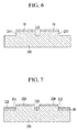
- FIG. 6 schematically illustrates a second semiconductor substrate 200 , a third photoresist film pattern 70 formed on the second semiconductor substrate 200 according to an exemplary embodiment of the present invention. Further, an alignment recess 210 , a first protrusion 211 , and a second protrusion 212 formed on the second semiconductor substrate 200 are formed by etching according to an exemplary embodiment of the present invention.
- FIG. 7 schematically illustrates a fourth photoresist film pattern 80 is formed on the second semiconductor substrate 200 , a second metal layer 220 formed on the second semiconductor substrate 200 and the fourth photoresist film pattern 80 according to an exemplary embodiment of the present invention.
- FIG. 8 schematically illustrates a third metal layer pattern 221 and a fourth metal layer pattern 222 may be formed on the first protrusion 211 and the second protrusion 212 , respectively, after the fourth photoresist film pattern 80 is removed according to an exemplary embodiment of the present invention.
- FIG. 9 schematically illustrates that the first semiconductor substrate 100 and the second semiconductor substrate 200 are joined according to an exemplary embodiment of the present invention.
- FIGS. 1-9 Reference numerals set forth in the FIGS. 1-9 include reference to the following elements as further discussed below:
- First semiconductor substrate 110 Alignment key 120: Insulating layer 130: First metal layer 131: First metal layer pattern 132: Second metal layer pattern 200: Second semiconductor substrate 210: Alignment recess 211: First protrusion 212: Second protrusion 220: Second metal layer 221: Third metal layer pattern 222: Fourth metal layer pattern 300: Joined metal layer
- the term “about” is understood as within a range of normal tolerance in the art, for example within 2 standard deviations of the mean. “About” can be understood as within 10%, 9%, 8%, 7%, 6%, 5%, 4%, 3%, 2%, 1%, 0.5%, 0.1%, 0.05%, or 0.01% of the stated value. Unless otherwise clear from the context, all numerical values provided herein are modified by the term “about”.
- FIGS. 1 to 9 A process of joining semiconductor substrates according to an exemplary embodiment of the present invention will be described with reference in FIGS. 1 to 9 .
- FIGS. 1 to 9 are cross-sectional views illustrating exemplary processes of the method of joining semiconductor substrates according to an exemplary embodiment of the present invention.
- a first semiconductor substrate 100 may be prepared, and subsequently a first photoresist film pattern 50 may be formed on the first semiconductor substrate 100 .
- an alignment key 110 may be formed by etching the first semiconductor substrate 100 by using the first photoresist film pattern 50 as a mask. The etching may be performed through dry etching or wet etching, without limitation. In particular, the alignment key 110 may formed by etching the first semiconductor substrate 100 , and a material for forming the alignment key 110 may not be required.
- an insulating layer 120 may be formed on the first semiconductor substrate 100 and the alignment key 110 .
- the insulating layer 120 may be formed of an insulating material, including silicon oxide (SiO 2 ), without limitation.
- a second photoresist film pattern 60 may be formed on the insulating layer 120 , and subsequently a first metal layer 130 may be formed on the insulating layer 120 and the second photoresist film pattern 60 .
- the second photoresist film pattern 60 may be removed from the first semiconductor substrate 100 by performing a lift-off process.
- the first metal layer 130 positioned on the second photoresist film pattern 60 may be removed.
- the first metal pattern 131 and the second metal pattern 132 may be formed on the insulating layer 120 .
- the first metal pattern 131 and the second metal pattern 132 may be formed by the lift-off process without using a mask, without limitation.
- the first metal pattern 131 and the second metal pattern 132 may be formed by using a mask.
- the first metal pattern 131 and the second metal pattern 132 may be formed by etching the first metal layer 130 by using a mask.
- a second semiconductor substrate 200 may be prepared, a third photoresist film pattern 70 may be formed on the second semiconductor substrate 200 .
- the second semiconductor substrate 200 may be etched by using the third photoresist film pattern 70 as a mask, without limitation.
- the etching may be performed through dry etching or wet etching, without limitation.
- an alignment recess 210 , a first protrusion 211 , and a second protrusion 212 may be formed on the second semiconductor substrate 200 .
- the alignment recess 210 may be positioned between the first protrusion 211 and the second protrusion 212 .
- a second metal layer 220 may be formed on the second semiconductor substrate 200 and the fourth photoresist film pattern 80 .
- the fourth photoresist film pattern 80 may not be formed in the first protrusion 211 and the second protrusion 212 of the second semiconductor substrate 200 . Accordingly, only the second metal layer 220 may be formed on the first protrusion 211 and the second protrusion 212 of the second semiconductor substrate 200 .
- the fourth photoresist film pattern 80 may be removed from the second semiconductor substrate 200 by the lift-off process.
- the second metal layer 220 positioned on the fourth photoresist film pattern 80 may be removed.
- a third metal layer pattern 221 and a fourth metal layer pattern 222 may be formed on the first protrusion 211 and the second protrusion 212 of the second semiconductor substrate 200 , respectively.
- the third metal layer pattern 221 and the fourth metal layer pattern 222 may be formed by the lift-off process without using a mask, without limitation, or the third metal layer pattern 221 and the fourth metal layer pattern 222 may also be formed by using a mask.
- the second metal layer 220 may be formed on the second semiconductor substrate 200 without forming the fourth photoresist film pattern 80 , and then the third metal layer pattern 221 and the fourth metal layer pattern 222 may be formed by etching the second metal layer 220 by using a mask.
- the first semiconductor substrate 100 and the second semiconductor substrate 200 may be joined.
- the alignment key 110 positioned in the first semiconductor substrate 100 may be positioned at the alignment recess 210 of the second semiconductor substrate 200 .
- the alignment key 110 may be positioned at the alignment recess 210 when the first semiconductor substrate 100 and the second semiconductor substrate 200 are joined, thereby joining the first semiconductor substrate 100 and the second semiconductor substrate 200 without an alignment error.
- the first metal layer pattern 131 and the third metal layer pattern 221 may be joined, and the second metal layer pattern 132 and the fourth metal layer pattern 222 may be joined, thereby forming joined metal layers 300 .
- a thickness of the alignment key 110 may be greater than that of the joined metal layers 300 .
- the joined metal layers 300 may reflow and flow down by the heat and the pressure and the reflow joined metal layers 300 may flow down and be connected with each other.
- the alignment key 110 may be positioned in the alignment recess 210 disposed between the first protrusion 211 and the second protrusion 212 , and the thickness of the alignment key 110 may be greater than the thickness of the joined metal layers 300 , the joined metal layers 300 may be prevented from being connected with each other, although the joined metal layers 300 may reflow and flow down. Accordingly, when the semiconductor device is formed by joining the first semiconductor substrate 100 and the second semiconductor substrate 200 , a defect of the semiconductor device may be prevented.
- a plurality of semiconductor devices may be generally formed in the semiconductor substrate. Accordingly, a plurality of alignment keys 110 may be formed in the first semiconductor substrate 100 . Moreover, a plurality of alignment recesses 210 corresponding to the alignment keys 110 may also be formed in the second semiconductor substrate 200 .
- exemplary processes of the method of joining the two semiconductor substrates according to various exemplary embodiments of the invention are described, but the present invention is not limited thereto.
- three or more semiconductor substrates may be joined by the aforementioned joining method.
- another alignment recess may be formed on an opposite surface of a portion in which the alignment recess 210 of the second semiconductor substrate 200 is formed, and then, another substrate, such as a third semiconductor substrate, in which a alignment key and a metal layer is formed may be joined to the second semiconductor substrate 200 .
- the alignment key of the third semiconductor substrate may be positioned to another alignment recess of the second semiconductor substrate 200 .
Abstract
Description
| 100: First semiconductor substrate | 110: Alignment key |
| 120: Insulating layer | 130: First metal layer |
| 131: First metal layer pattern | 132: Second metal layer pattern |
| 200: Second semiconductor substrate | 210: Alignment recess |
| 211: First protrusion | 212: Second protrusion |
| 220: Second metal layer | 221: Third metal layer pattern |
| 222: Fourth metal layer pattern | 300: Joined metal layer |
Claims (7)
Applications Claiming Priority (2)
| Application Number | Priority Date | Filing Date | Title |
|---|---|---|---|
| KR1020130167810A KR101542965B1 (en) | 2013-12-30 | 2013-12-30 | Method for junction of semiconductor substrate |
| KR10-2013-0167810 | 2013-12-30 |
Publications (2)
| Publication Number | Publication Date |
|---|---|
| US20150187704A1 US20150187704A1 (en) | 2015-07-02 |
| US9312227B2 true US9312227B2 (en) | 2016-04-12 |
Family
ID=53482685
Family Applications (1)
| Application Number | Title | Priority Date | Filing Date |
|---|---|---|---|
| US14/445,653 Active US9312227B2 (en) | 2013-12-30 | 2014-07-29 | Method of joining semiconductor substrate |
Country Status (3)
| Country | Link |
|---|---|
| US (1) | US9312227B2 (en) |
| KR (1) | KR101542965B1 (en) |
| CN (1) | CN104752342B (en) |
Families Citing this family (3)
| Publication number | Priority date | Publication date | Assignee | Title |
|---|---|---|---|---|
| RU2680263C1 (en) * | 2017-12-11 | 2019-02-19 | Публичное акционерное общество Арзамасское научно-производственное предприятие "ТЕМП-АВИА" | Method of connecting silicon plates |
| US10529593B2 (en) * | 2018-04-27 | 2020-01-07 | Taiwan Semiconductor Manufacturing Co., Ltd. | Semiconductor package comprising molding compound having extended portion and manufacturing method of semiconductor package |
| KR102145879B1 (en) * | 2019-06-07 | 2020-08-19 | 한국생산기술연구원 | Mimic mask for analyzing a cleaning process of fine metal mask, analyzing method using the same, and manufacturing method thereof |
Citations (9)
| Publication number | Priority date | Publication date | Assignee | Title |
|---|---|---|---|---|
| JPH11266005A (en) | 1998-03-16 | 1999-09-28 | Canon Inc | Substrate junction method using positive pressure impression and element structure thereof |
| JP2000091174A (en) | 1998-09-14 | 2000-03-31 | Canon Inc | Method of forming functional bond at bonding region by inter-substrate joint reinforced by application of positive pressure and element structure having functional bond |
| KR20030094454A (en) | 2002-06-04 | 2003-12-12 | 주식회사 하이닉스반도체 | Align key of semiconductor device |
| JP2005079070A (en) | 2003-09-04 | 2005-03-24 | Canon Inc | Board-to-board electrode jointing method and structure |
| US20060049408A1 (en) * | 2004-09-09 | 2006-03-09 | Woo-Sung Sohn | Display device and method of manufacturing the same |
| KR20110134114A (en) | 2010-06-08 | 2011-12-14 | 삼성코닝정밀소재 주식회사 | Method for producing bonded substrates |
| US8119498B2 (en) | 2008-09-24 | 2012-02-21 | Evigia Systems, Inc. | Wafer bonding method and wafer stack formed thereby |
| KR20120126210A (en) | 2011-05-11 | 2012-11-21 | (주)한비젼 | Wafer for thin film transfer having a plurality of alignment keys for 3D stacking structure |
| US20140139924A1 (en) * | 2011-05-16 | 2014-05-22 | Hamamatsu Photonics K.K. | Optical module and production method for same |
Family Cites Families (6)
| Publication number | Priority date | Publication date | Assignee | Title |
|---|---|---|---|---|
| US5477086A (en) * | 1993-04-30 | 1995-12-19 | Lsi Logic Corporation | Shaped, self-aligning micro-bump structures |
| US6495396B1 (en) * | 2001-08-29 | 2002-12-17 | Sun Microsystems, Inc. | Method of coupling and aligning semiconductor devices including multi-chip semiconductor devices |
| JP2005107452A (en) * | 2003-10-02 | 2005-04-21 | Sony Corp | Method for manufacturing liquid crystal display element, liquid crystal display element, projection display apparatus and method for laminating substrate |
| US7652374B2 (en) * | 2006-07-31 | 2010-01-26 | Chi Wah Kok | Substrate and process for semiconductor flip chip package |
| WO2008084811A1 (en) * | 2007-01-10 | 2008-07-17 | Hitachi Chemical Company, Ltd. | Adhesive for connection of circuit member and semiconductor device using the same |
| US8349653B2 (en) * | 2010-06-02 | 2013-01-08 | Maxim Integrated Products, Inc. | Use of device assembly for a generalization of three-dimensional metal interconnect technologies |
-
2013
- 2013-12-30 KR KR1020130167810A patent/KR101542965B1/en active IP Right Grant
-
2014
- 2014-07-29 US US14/445,653 patent/US9312227B2/en active Active
- 2014-08-28 CN CN201410433157.3A patent/CN104752342B/en active Active
Patent Citations (9)
| Publication number | Priority date | Publication date | Assignee | Title |
|---|---|---|---|---|
| JPH11266005A (en) | 1998-03-16 | 1999-09-28 | Canon Inc | Substrate junction method using positive pressure impression and element structure thereof |
| JP2000091174A (en) | 1998-09-14 | 2000-03-31 | Canon Inc | Method of forming functional bond at bonding region by inter-substrate joint reinforced by application of positive pressure and element structure having functional bond |
| KR20030094454A (en) | 2002-06-04 | 2003-12-12 | 주식회사 하이닉스반도체 | Align key of semiconductor device |
| JP2005079070A (en) | 2003-09-04 | 2005-03-24 | Canon Inc | Board-to-board electrode jointing method and structure |
| US20060049408A1 (en) * | 2004-09-09 | 2006-03-09 | Woo-Sung Sohn | Display device and method of manufacturing the same |
| US8119498B2 (en) | 2008-09-24 | 2012-02-21 | Evigia Systems, Inc. | Wafer bonding method and wafer stack formed thereby |
| KR20110134114A (en) | 2010-06-08 | 2011-12-14 | 삼성코닝정밀소재 주식회사 | Method for producing bonded substrates |
| KR20120126210A (en) | 2011-05-11 | 2012-11-21 | (주)한비젼 | Wafer for thin film transfer having a plurality of alignment keys for 3D stacking structure |
| US20140139924A1 (en) * | 2011-05-16 | 2014-05-22 | Hamamatsu Photonics K.K. | Optical module and production method for same |
Also Published As
| Publication number | Publication date |
|---|---|
| CN104752342A (en) | 2015-07-01 |
| KR20150078447A (en) | 2015-07-08 |
| KR101542965B1 (en) | 2015-08-07 |
| US20150187704A1 (en) | 2015-07-02 |
| CN104752342B (en) | 2019-04-02 |
Similar Documents
| Publication | Publication Date | Title |
|---|---|---|
| US9862595B2 (en) | Method for manufacturing thin-film support beam | |
| CN108206142B (en) | Bonding alignment precision detection method and semiconductor device | |
| US20160126136A1 (en) | Semiconductor device and method for manufacturing semiconductor device | |
| JP2009111375A5 (en) | ||
| TWI475640B (en) | A method of fabricating a multilayer structure with circuit layer transfer | |
| US20170205705A1 (en) | Pellicle and method for manufacturing the same | |
| US9312227B2 (en) | Method of joining semiconductor substrate | |
| JP4620939B2 (en) | Method for manufacturing composite element | |
| US11754758B2 (en) | Optical diffuser and its method of manufacture | |
| US9613904B2 (en) | Semiconductor structure and manufacturing method thereof | |
| US9681244B1 (en) | Method for manufacturing microphone chip | |
| WO2016127618A1 (en) | Manufacturing method for array substrate, array substrate and display device | |
| CN106653578B (en) | Wafer processing method | |
| KR20110010326A (en) | Fabrication method of soi(silicon on insulator) wafer | |
| US7192842B2 (en) | Method for bonding wafers | |
| US20060030082A1 (en) | Semiconductor device and fabricating method thereof | |
| CN106716620B (en) | Semiconductor structure with multiple active layers in SOI wafer | |
| KR101534705B1 (en) | Method for junction of semiconductor substrate | |
| CN105573045B (en) | Photomask, manufacturing method of semiconductor device and semiconductor device | |
| JP2007135129A (en) | Manufacturing method of piezoelectric vibrating piece and piezoelectric vibrating piece manufactured by method | |
| TWI570873B (en) | Semiconductor structure and manufacturing method for the same | |
| WO2010103592A1 (en) | Semiconductor device and method for manufacturing same | |
| US20060292828A1 (en) | Wafer and method of cutting the same | |
| TWI639365B (en) | Circuit substrate and manufacturing method of circuit substrate | |
| KR20120122634A (en) | Method for forming overlay vernier |
Legal Events
| Date | Code | Title | Description |
|---|---|---|---|
| AS | Assignment |
Owner name: HYUNDAI MOTOR COMPANY, KOREA, REPUBLIC OF Free format text: ASSIGNMENT OF ASSIGNORS INTEREST;ASSIGNORS:YOO, ILSEON;LEE, HIWON;KWON, SOON-MYUNG;AND OTHERS;REEL/FRAME:034086/0231 Effective date: 20140618 |
|
| FEPP | Fee payment procedure |
Free format text: PAYER NUMBER DE-ASSIGNED (ORIGINAL EVENT CODE: RMPN); ENTITY STATUS OF PATENT OWNER: LARGE ENTITY Free format text: PAYOR NUMBER ASSIGNED (ORIGINAL EVENT CODE: ASPN); ENTITY STATUS OF PATENT OWNER: LARGE ENTITY |
|
| STCF | Information on status: patent grant |
Free format text: PATENTED CASE |
|
| MAFP | Maintenance fee payment |
Free format text: PAYMENT OF MAINTENANCE FEE, 4TH YEAR, LARGE ENTITY (ORIGINAL EVENT CODE: M1551); ENTITY STATUS OF PATENT OWNER: LARGE ENTITY Year of fee payment: 4 |
|
| MAFP | Maintenance fee payment |
Free format text: PAYMENT OF MAINTENANCE FEE, 8TH YEAR, LARGE ENTITY (ORIGINAL EVENT CODE: M1552); ENTITY STATUS OF PATENT OWNER: LARGE ENTITY Year of fee payment: 8 |