US9246453B2 - Tunable RF filter - Google Patents
Tunable RF filter Download PDFInfo
- Publication number
- US9246453B2 US9246453B2 US12/678,507 US67850708A US9246453B2 US 9246453 B2 US9246453 B2 US 9246453B2 US 67850708 A US67850708 A US 67850708A US 9246453 B2 US9246453 B2 US 9246453B2
- Authority
- US
- United States
- Prior art keywords
- transistor
- emitter
- tunable
- stage
- emitter follower
- Prior art date
- Legal status (The legal status is an assumption and is not a legal conclusion. Google has not performed a legal analysis and makes no representation as to the accuracy of the status listed.)
- Active, expires
Links
Images


Classifications
-
- H—ELECTRICITY
- H03—ELECTRONIC CIRCUITRY
- H03F—AMPLIFIERS
- H03F3/00—Amplifiers with only discharge tubes or only semiconductor devices as amplifying elements
- H03F3/50—Amplifiers in which input is applied to, or output is derived from, an impedance common to input and output circuits of the amplifying element, e.g. cathode follower
-
- H—ELECTRICITY
- H03—ELECTRONIC CIRCUITRY
- H03F—AMPLIFIERS
- H03F1/00—Details of amplifiers with only discharge tubes, only semiconductor devices or only unspecified devices as amplifying elements
- H03F1/26—Modifications of amplifiers to reduce influence of noise generated by amplifying elements
-
- H—ELECTRICITY
- H03—ELECTRONIC CIRCUITRY
- H03F—AMPLIFIERS
- H03F1/00—Details of amplifiers with only discharge tubes, only semiconductor devices or only unspecified devices as amplifying elements
- H03F1/32—Modifications of amplifiers to reduce non-linear distortion
-
- H—ELECTRICITY
- H03—ELECTRONIC CIRCUITRY
- H03F—AMPLIFIERS
- H03F1/00—Details of amplifiers with only discharge tubes, only semiconductor devices or only unspecified devices as amplifying elements
- H03F1/34—Negative-feedback-circuit arrangements with or without positive feedback
-
- H—ELECTRICITY
- H03—ELECTRONIC CIRCUITRY
- H03F—AMPLIFIERS
- H03F1/00—Details of amplifiers with only discharge tubes, only semiconductor devices or only unspecified devices as amplifying elements
- H03F1/56—Modifications of input or output impedances, not otherwise provided for
-
- H—ELECTRICITY
- H03—ELECTRONIC CIRCUITRY
- H03F—AMPLIFIERS
- H03F3/00—Amplifiers with only discharge tubes or only semiconductor devices as amplifying elements
- H03F3/189—High-frequency amplifiers, e.g. radio frequency amplifiers
- H03F3/19—High-frequency amplifiers, e.g. radio frequency amplifiers with semiconductor devices only
- H03F3/195—High-frequency amplifiers, e.g. radio frequency amplifiers with semiconductor devices only in integrated circuits
-
- H—ELECTRICITY
- H03—ELECTRONIC CIRCUITRY
- H03F—AMPLIFIERS
- H03F3/00—Amplifiers with only discharge tubes or only semiconductor devices as amplifying elements
- H03F3/45—Differential amplifiers
- H03F3/45071—Differential amplifiers with semiconductor devices only
- H03F3/45076—Differential amplifiers with semiconductor devices only characterised by the way of implementation of the active amplifying circuit in the differential amplifier
- H03F3/45475—Differential amplifiers with semiconductor devices only characterised by the way of implementation of the active amplifying circuit in the differential amplifier using IC blocks as the active amplifying circuit
-
- H—ELECTRICITY
- H03—ELECTRONIC CIRCUITRY
- H03G—CONTROL OF AMPLIFICATION
- H03G5/00—Tone control or bandwidth control in amplifiers
- H03G5/02—Manually-operated control
- H03G5/14—Manually-operated control in frequency-selective amplifiers
-
- H—ELECTRICITY
- H03—ELECTRONIC CIRCUITRY
- H03H—IMPEDANCE NETWORKS, e.g. RESONANT CIRCUITS; RESONATORS
- H03H11/00—Networks using active elements
- H03H11/02—Multiple-port networks
- H03H11/04—Frequency selective two-port networks
- H03H11/12—Frequency selective two-port networks using amplifiers with feedback
- H03H11/1213—Frequency selective two-port networks using amplifiers with feedback using transistor amplifiers
-
- H—ELECTRICITY
- H03—ELECTRONIC CIRCUITRY
- H03H—IMPEDANCE NETWORKS, e.g. RESONANT CIRCUITS; RESONATORS
- H03H11/00—Networks using active elements
- H03H11/02—Multiple-port networks
- H03H11/04—Frequency selective two-port networks
- H03H11/12—Frequency selective two-port networks using amplifiers with feedback
- H03H11/1291—Current or voltage controlled filters
-
- H—ELECTRICITY
- H03—ELECTRONIC CIRCUITRY
- H03F—AMPLIFIERS
- H03F2200/00—Indexing scheme relating to amplifiers
- H03F2200/144—Indexing scheme relating to amplifiers the feedback circuit of the amplifier stage comprising a passive resistor and passive capacitor
-
- H—ELECTRICITY
- H03—ELECTRONIC CIRCUITRY
- H03F—AMPLIFIERS
- H03F2200/00—Indexing scheme relating to amplifiers
- H03F2200/213—A variable capacitor being added in the input circuit, e.g. base, gate, of an amplifier stage
-
- H—ELECTRICITY
- H03—ELECTRONIC CIRCUITRY
- H03F—AMPLIFIERS
- H03F2200/00—Indexing scheme relating to amplifiers
- H03F2200/378—A variable capacitor being added in the output circuit, e.g. collector, drain, of an amplifier stage
-
- H—ELECTRICITY
- H03—ELECTRONIC CIRCUITRY
- H03F—AMPLIFIERS
- H03F2200/00—Indexing scheme relating to amplifiers
- H03F2200/408—Indexing scheme relating to amplifiers the output amplifying stage of an amplifier comprising three power stages
-
- H—ELECTRICITY
- H03—ELECTRONIC CIRCUITRY
- H03F—AMPLIFIERS
- H03F2200/00—Indexing scheme relating to amplifiers
- H03F2200/411—Indexing scheme relating to amplifiers the output amplifying stage of an amplifier comprising two power stages
-
- H—ELECTRICITY
- H03—ELECTRONIC CIRCUITRY
- H03F—AMPLIFIERS
- H03F2200/00—Indexing scheme relating to amplifiers
- H03F2200/435—A peak detection being used in a signal measuring circuit in a controlling circuit of an amplifier
-
- H—ELECTRICITY
- H03—ELECTRONIC CIRCUITRY
- H03F—AMPLIFIERS
- H03F2200/00—Indexing scheme relating to amplifiers
- H03F2200/451—Indexing scheme relating to amplifiers the amplifier being a radio frequency amplifier
-
- H—ELECTRICITY
- H03—ELECTRONIC CIRCUITRY
- H03F—AMPLIFIERS
- H03F2203/00—Indexing scheme relating to amplifiers with only discharge tubes or only semiconductor devices as amplifying elements covered by H03F3/00
- H03F2203/45—Indexing scheme relating to differential amplifiers
- H03F2203/45136—One differential amplifier in IC-block form being shown
-
- H—ELECTRICITY
- H03—ELECTRONIC CIRCUITRY
- H03F—AMPLIFIERS
- H03F2203/00—Indexing scheme relating to amplifiers with only discharge tubes or only semiconductor devices as amplifying elements covered by H03F3/00
- H03F2203/45—Indexing scheme relating to differential amplifiers
- H03F2203/45522—Indexing scheme relating to differential amplifiers the FBC comprising one or more potentiometers
-
- H—ELECTRICITY
- H03—ELECTRONIC CIRCUITRY
- H03F—AMPLIFIERS
- H03F2203/00—Indexing scheme relating to amplifiers with only discharge tubes or only semiconductor devices as amplifying elements covered by H03F3/00
- H03F2203/50—Indexing scheme relating to amplifiers in which input being applied to, or output being derived from, an impedance common to input and output circuits of the amplifying element, e.g. cathode follower
- H03F2203/5006—Indexing scheme relating to amplifiers in which input being applied to, or output being derived from, an impedance common to input and output circuits of the amplifying element, e.g. cathode follower the input signal being capacitively coupled to the gate of the source follower
-
- H—ELECTRICITY
- H03—ELECTRONIC CIRCUITRY
- H03F—AMPLIFIERS
- H03F2203/00—Indexing scheme relating to amplifiers with only discharge tubes or only semiconductor devices as amplifying elements covered by H03F3/00
- H03F2203/50—Indexing scheme relating to amplifiers in which input being applied to, or output being derived from, an impedance common to input and output circuits of the amplifying element, e.g. cathode follower
- H03F2203/5021—Indexing scheme relating to amplifiers in which input being applied to, or output being derived from, an impedance common to input and output circuits of the amplifying element, e.g. cathode follower the source follower has a controlled source circuit
-
- H—ELECTRICITY
- H03—ELECTRONIC CIRCUITRY
- H03F—AMPLIFIERS
- H03F2203/00—Indexing scheme relating to amplifiers with only discharge tubes or only semiconductor devices as amplifying elements covered by H03F3/00
- H03F2203/50—Indexing scheme relating to amplifiers in which input being applied to, or output being derived from, an impedance common to input and output circuits of the amplifying element, e.g. cathode follower
- H03F2203/5024—Indexing scheme relating to amplifiers in which input being applied to, or output being derived from, an impedance common to input and output circuits of the amplifying element, e.g. cathode follower the source follower has a controlled source circuit, the source circuit being controlled via a capacitor, i.e. AC-controlled
-
- H—ELECTRICITY
- H03—ELECTRONIC CIRCUITRY
- H03F—AMPLIFIERS
- H03F2203/00—Indexing scheme relating to amplifiers with only discharge tubes or only semiconductor devices as amplifying elements covered by H03F3/00
- H03F2203/50—Indexing scheme relating to amplifiers in which input being applied to, or output being derived from, an impedance common to input and output circuits of the amplifying element, e.g. cathode follower
- H03F2203/5031—Indexing scheme relating to amplifiers in which input being applied to, or output being derived from, an impedance common to input and output circuits of the amplifying element, e.g. cathode follower the source circuit of the follower being a current source
-
- H—ELECTRICITY
- H03—ELECTRONIC CIRCUITRY
- H03F—AMPLIFIERS
- H03F2203/00—Indexing scheme relating to amplifiers with only discharge tubes or only semiconductor devices as amplifying elements covered by H03F3/00
- H03F2203/50—Indexing scheme relating to amplifiers in which input being applied to, or output being derived from, an impedance common to input and output circuits of the amplifying element, e.g. cathode follower
- H03F2203/5036—Indexing scheme relating to amplifiers in which input being applied to, or output being derived from, an impedance common to input and output circuits of the amplifying element, e.g. cathode follower the source follower has a resistor in its source circuit
-
- H—ELECTRICITY
- H03—ELECTRONIC CIRCUITRY
- H03F—AMPLIFIERS
- H03F2203/00—Indexing scheme relating to amplifiers with only discharge tubes or only semiconductor devices as amplifying elements covered by H03F3/00
- H03F2203/50—Indexing scheme relating to amplifiers in which input being applied to, or output being derived from, an impedance common to input and output circuits of the amplifying element, e.g. cathode follower
- H03F2203/5039—Indexing scheme relating to amplifiers in which input being applied to, or output being derived from, an impedance common to input and output circuits of the amplifying element, e.g. cathode follower the source circuit of the follower has one or more capacitors between source and supply
Definitions
- the present invention relates to tunable radio frequency (RF) filters, including tracking filters, and circuits therefor.
- RF radio frequency
- the present invention is particularly suited to, but not limited to, tunable RF filters for incorporation in wideband receivers, for example tuner circuits for VHF and UHF channels of television signals.
- tunable RF filters including tracking filters
- the discrete components include varactors, inductors, capacitors and/or switchable diodes.
- OTAs operational transconductance amplifiers
- U.S. Pat. No. 6,915,121 describes a corresponding tunable RF filter circuit in which transistors are used to implement the differential amplifiers, i.e. the tunable RF filter circuit of U.S. Pat. No. 6,915,121 includes two differential pairs of transistors.
- the present inventors have realised it would be desirable to provide a transistor based tunable RF filter circuit that does not use differential amplifiers or differential pairs of transistors.
- the present inventors have realised that such a circuit would tend to suffer less noise than ones with differential amplifiers, especially ones with differential pairs of transistors.
- the present inventors have further realised that a limitation of known filter circuits such as those mentioned above is that such filters tend to suffer from non-linearity with respect to varying input voltage level, and that consequently it would be desirable to provide a tunable RF filter circuit design with improved linearity in terms of gain as a function of input voltage signal level, i.e. it would be desirable to provide a tunable RF filter circuit design with “in-built” automatic gain control functionality.
- the present invention provides a tunable RF filter, comprising: an emitter follower stage; and a common emitter stage; wherein the common emitter stage is arranged to provide feedback to the emitter follower stage.
- the common emitter stage may comprise a first transistor, the first transistor being the only transistor of the common emitter stage.
- the emitter follower stage may comprise a second transistor, the second transistor being the only transistor of the emitter follower stage.
- the feedback may be provided from the collector terminal of the first transistor to the base terminal of the second transistor.
- An output derived from the emitter terminal of the second transistor may be provided to the base terminal of the first transistor.
- the base terminal of the second transistor may be connected via a first capacitor to a voltage signal input terminal, the emitter terminal of the first transistor may be connected to ground via a first resistor, and the emitter terminal of the second transistor may be connected to ground via a second resistor and a second capacitor in series, and one or more of the first resistor, the second resistor, the first capacitor and the second capacitor may be a variable value component.
- the present invention provides a tunable RF filter, comprising: an emitter follower stage; a joint common emitter and emitter follower stage; and a gain stage; wherein a common emitter output of the joint common emitter and emitter follower stage is arranged to provide feedback to the emitter follower stage, and an emitter follower output of the joint common emitter and emitter follower stage is arranged to provide an input to the gain stage.
- the joint common emitter and emitter follower stage may comprise a first transistor, the first transistor being the only transistor of the joint common emitter and emitter follower stage.
- the emitter follower stage may comprise a second transistor, the second transistor being the only transistor of the emitter follower stage.
- the feedback may be provided from the collector terminal of the first transistor to the base terminal of the second transistor.
- An output derived from the emitter terminal of the second transistor may be provided to the base terminal of the first transistor.
- the base terminal of the second transistor may be connected via a first capacitor to a voltage signal input terminal, the emitter terminal of the first transistor may be connected to the gain stage via a first resistor, and the emitter terminal of the second transistor may be connected to ground via a second resistor and a second capacitor in series, and one or more of the first resistor, the second resistor, the first capacitor and the second capacitor may be a variable value component.
- the gain stage may further comprise a fine gain tuning functionality.
- the fine gain tuning functionality may comprise a variable value resistor.
- FIG. 1 is a block diagram of a tunable RF filter
- FIG. 2 is a circuit diagram of a particular tunable RF filter circuit implementing the tunable RF filter of FIG. 1 ;
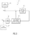
- FIG. 3 is a block diagram of a further tunable RF filter.
- FIG. 4 is a circuit diagram of a particular tunable RF filter circuit implementing the tunable RF filter of FIG. 3 .
- FIG. 1 is a block diagram of a tunable RF filter 1 , which may be referred to as a tracking filter, according to a first embodiment.
- the tunable RF filter 1 comprises an emitter follower stage 2 and a common emitter stage 4 .
- An input RF signal V in is coupled to the input of the emitter follower stage 2 .
- the output of the emitter follower stage 2 provides the output signal V out of the tunable RF filter 1 .
- the output of the emitter follower stage 2 is also provided as an input to the common emitter stage 4 .
- the output of the common emitter stage 4 is coupled to the input of the emitter follower stage 2 , i.e. is added to the input RF signal V in to provide a combined input to the emitter follower stage 2 .
- the common emitter stage 4 provides a form of feedback to the emitter follower stage 2 .
- FIG. 2 is a circuit diagram of a particular tunable RF filter circuit 11 implementing, according to this embodiment, the tunable RF filter 1 of FIG. 1 .
- the tunable RF filter circuit 11 comprises only two transistors, namely T 1 and T 2 .
- the transistors T 1 and T 2 are bipolar transistors.
- other types of transistors may be used, for example MOS transistors.
- Transistor T 2 is arranged as an emitter follower, as follows.
- the collector terminal of transistor T 2 is connected to voltage Vcc, which is the power supply voltage for the tunable RF filter circuit 11 .
- the base terminal of transistor T 2 is connected to a variable capacitor C 1 and also to the collector terminal of transistor T 1 .
- the emitter terminal of transistor T 2 is connected to a variable resistor R 2 and also to a current source CS 2 delivering a current of value I 2 .
- the other connection of the current source CS 2 is connected to ground.
- the other connection of the variable capacitor C 1 is connected to V in , the input RF signal voltage.
- the other connection of the variable resistor R 2 is connected to a further variable capacitor C 2 and to the input of a unity gain amplifier A 2 .
- the other connection of the variable capacitor C 2 is connected to ground.
- the output of the amplifier A 2 provides V out , the output signal voltage.
- Transistor T 1 is arranged as a common emitter, as follows.
- the output of amplifier A 2 is also connected to the base terminal of transistor T 1 .
- the collector terminal of transistor T 1 is also connected to an impedance Z H .
- the emitter terminal of T 1 is connected to a variable resistor R 1 and also to a current source CS 1 delivering a current of value I 1 .
- the other connection of the current source CS 1 is connected to ground.
- the other connection of the variable resistor R 1 is connected to a capacitor C c .
- the other connection of the capacitor C c is connected to ground.
- the other connection of the impedance Z H is connected to Vcc.
- the impedance Z H is of high impedance, and may be considered as constituted by a frequency dependent inductor L in series with a substantially frequency-independent impedance Z B , and operates as a current source.
- the transistor T 2 , the variable resistor R 2 , the current source CS 2 , the variable capacitor C 2 and the unity gain amplifier A 2 together constitute an emitter follower stage 2 corresponding to the emitter follower stage 2 of FIG. 1 ; and the transistor T 1 , the current source CS 1 , the variable resistor R 1 and the capacitor C c together constitute a common emitter stage 4 corresponding to the common emitter stage 4 of FIG. 1 .
- the collector terminal of transistor T 1 provides an output of the common emitter stage 4 , and this output is coupled to the input of the emitter follower stage 2 , i.e. the base terminal of T 2 , moreover being added to the input RF signal V in to provide a combined input to the emitter follower stage 2 .
- the common emitter stage 4 provides a form of feedback to the emitter follower stage 2 .
- the unity gain amplifier A 2 serves to provide impedance matching for the output signal voltage V out .
- variable resistors R 1 and R 2 may perform various functions. Firstly they increase the linearity of their respective stage. Secondly, along with the variable capacitors C 1 and C 2 , they may be used to control operating parameters such as central frequency, as will be described in more detail below.
- the tunable RF filter circuit 11 provides various advantages over prior art circuits.
- the tunable RF filter circuit 11 provides a transistor based tunable RF filter circuit that does not use differential amplifiers or differential pairs of transistors.
- the tunable RF filter circuit 11 therefore tends to suffer less noise than prior art ones with differential amplifiers, especially ones with differential pairs of transistors.
- the simplified design of the tunable RF filter circuit 11 (again, the use of only two transistors, and also fewer current sources) compared to prior art circuits tends to allow more efficient and cost effective manufacture, more reliable operation, and so on.
- the design of the tunable RF filter circuit 11 allows straightforward control of various operating parameters, in particular by variation of one or more of the variable components comprising the variable resistors R 1 and R 2 and the variable capacitors C 1 and C 2 .
- This aspect can further be appreciated from the following analysis:
- the transfer function of the band pass filter is:
- V out V in p ⁇ gm 2 C 2 ⁇ ( 1 + gm 2 ⁇ R 2 ) p 2 + p ⁇ gm 2 C 2 ⁇ ( 1 + gm 2 ⁇ R 2 ) + gm 1 ⁇ gm 2 C 1 ⁇ C 2 ⁇ ( 1 + gm 2 ⁇ R 2 ) ⁇ ( 1 + gm 1 ⁇ R 1 ) ( 1.1 )
- gm 1 is the transconductance gain of the common emitter stage 4
- gm 2 is the transconductance gain of the emitter follower stage 2 .
- the central frequency f 0 is:
- equation 1.2 shows how the central frequency f 0 can be varied by varying one or more of C 1 , C 2 , R 1 and R 2 ;
- equation 1.3 shows how the quality factor Q can be varied by varying one or more of C 1 , C 2 , R 1 and R 2 ;
- equation 1.4 shows how the bandwidth B can be varied by varying one or more of C 2 and R 2 ;
- equation 1.5 shows how the input impedance Z in can be varied by varying C 1 .
- the present inventors have further realised a disadvantage of the first embodiment and have also realised that this disadvantage is also exhibited by prior art circuits.
- the disadvantage, which the inventors have realised is indicated in equation 1.6, is that the gain between V 1 and V in is proportional to the quality factor Q, hence increasing the quality factor Q increases the gain at the input of transistor T 2 . Consequently, (as is also the case with prior art circuits) the RF filter circuit 11 displays non-linear gain with respect to the level of the input RF signal voltage V in , in particular for high levels of V in .
- FIG. 3 is a block diagram of a tunable RF filter 21 , which may be referred to as a tracking filter, according to the second embodiment.
- the tunable RF filter 1 comprises an emitter follower stage 22 and a joint common emitter and emitter follower stage 24 .
- An input RF signal V in is coupled to the input of the emitter follower stage 22 .
- the output of the emitter follower stage 22 is provided as an input to the joint common emitter and emitter follower stage 24 .
- a first output of the joint common emitter and emitter follower stage 24 is coupled to the input of the emitter follower stage 22 , i.e. is added to the input RF signal V in to provide a combined input to the emitter follower stage 22 .
- the joint common emitter and emitter follower stage 24 provides a form of feedback to the emitter follower stage 22 .
- a second output of the joint common emitter and emitter follower stage 24 is provided as an input to a gain stage 26 .
- the gain stage 26 is a fine tune and gain stage 26 .
- the output of the fine tune and gain stage 26 provides the output signal V out of the tunable RF filter 1 .
- a conventional level detector 28 is coupled to V in for detecting the signal level of V in .
- the level detector 28 is instead coupled to V out for detecting the signal level of V out , this latter alternative being indicated in FIG. 3 by a dotted line representation of the level detector 28 .
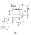
- FIG. 4 is a circuit diagram of a particular tunable RF filter circuit 31 implementing, according to this embodiment, the tunable RF filter 21 of FIG. 3 .
- the tunable RF filter circuit 31 comprises only two transistors, namely T 1 and T 2 .
- the transistors T 1 and T 2 are bipolar transistors.
- other types of transistors may be used, for example MOS transistors.
- Transistor T 2 is arranged as an emitter follower, as follows.
- the collector terminal of transistor T 2 is connected to voltage Vcc, which is the power supply voltage for the tunable RF filter circuit 31 .
- the base terminal of transistor T 2 is connected to a variable capacitor C 1 and also to the collector terminal of transistor T 1 .
- the emitter terminal of transistor T 2 is connected to a variable resistor R 2 and also to a current source CS 2 delivering a current of value I 2 .
- the other connection of the current source CS 2 is connected to ground.
- the other connection of the variable capacitor C 1 is connected to V in , the input RF signal voltage.
- the other connection of the variable resistor R 2 is connected to a further variable capacitor C 2 .
- the other connection of the variable capacitor C 2 is connected to ground.
- Transistor T 1 is arranged both as a common emitter and as an emitter follower, as follows.
- the above mentioned other connection of the variable resistor R 2 is also connected to the base terminal of transistor T 1 .
- the collector terminal of transistor T 1 is also connected to an impedance Z H .
- the emitter terminal of T 1 is connected to a variable resistor R 1 and also to a current source CS 1 delivering a current of value I 1 .
- the other connection of the current source CS 1 is connected to ground.
- the other connection of the variable resistor R 1 is connected to a capacitor C c .
- the other connection of the impedance Z H is connected to Vcc.
- the impedance Z H is of high impedance, and may be considered as constituted by a frequency dependent inductor L in series with a substantially frequency-independent impedance Z B , and operates as a current source.
- the tunable RF filter circuit 31 further comprises an amplifier A 3 and a further variable resistor R f .
- the negative input terminal of the amplifier A 3 is connected to the other connection of the capacitor C c .
- the positive input terminal of the amplifier A 3 is connected to ground.
- the variable resistor R f is connected across the amplifier A 3 , i.e. is connected between the negative input terminal of the amplifier A 3 and the output terminal of the amplifier A 3 .
- the output of the amplifier A 3 provides V out , the output signal voltage.
- a level detector 28 may be connected to V in .
- Another possibility is for the level detector 28 to be connected to V out , this latter possibility being indicated in FIG. 4 by a dotted line representation of the level detector 28 .
- the transistor T 2 , the variable resistor R 2 , the current source CS 2 , and the variable capacitor C 2 together constitute an emitter follower stage 22 corresponding to the emitter follower stage 22 of FIG. 3 ;
- the transistor T 1 , the current source CS 1 , the variable resistor R 1 and the capacitor C c together constitute a joint common emitter and emitter follower stage 24 corresponding to the joint common emitter and emitter follower stage 24 of FIG. 3 ;
- the amplifier A 3 and variable resistor R f together constitute a fine-tune and gain stage 26 corresponding to the fine tune and gain stage 26 of FIG. 3 .
- the collector terminal of transistor T 1 provides an output of the common emitter function of the joint common emitter and emitter follower stage 4 , and this output is coupled to the input of the emitter follower stage 2 , i.e. the base terminal of T 2 , moreover being added to the input RF signal V in to provide a combined input to the emitter follower stage 2 .
- the common emitter stage 4 provides a form of feedback to the emitter follower stage 2 .
- the emitter terminal of transistor T 1 provides an output of the emitter follower function of the joint common emitter and emitter follower stage 4 .
- This output provides an input signal to the fine tune and gain stage 26 .
- the fine tune and gain stage amplifies the signal to provide V out , the output signal voltage.
- variable resistor R f provides fine tuning of the gain of the amplifier A 3 , and hence fine-tuning of automatic gain control functionality performed by the tunable RF filter circuit 31 (the automatic gain control functionality will be described in more detail below).
- variable resistors R 1 and R 2 may perform various functions. Firstly they increase the linearity of their respective stage. Secondly, along with the variable capacitors C 1 and C 2 , they may be used to control operating parameters such as central frequency, along the lines described above in relation to FIGS. 1 and 2 . In this embodiment, R 1 additionally plays a role in the automatic gain control functionality performed by the tunable RF filter circuit 31 .
- the tunable RF filter circuit 31 provides various advantages over prior art circuits.
- the tunable RF filter circuit 31 provides a transistor based tunable RF filter circuit that does not use differential amplifiers or differential pairs of transistors.
- the tunable RF filter circuit 31 therefore tends to suffer less noise than prior art ones with differential amplifiers, especially ones with differential pairs of transistors.
- the simplified design of the tunable RF filter circuit 31 (again, the use of only two transistors, and also fewer current sources) compared to prior art circuits tends to allow more efficient and cost effective manufacture, more reliable operation, and so on.
- the design of the tunable RF filter circuit 31 allows straightforward control of various operating parameters, in particular by variation of one or more of the variable components comprising the variable resistors R f , R 1 and R 2 and the variable capacitors C 1 and C 2 .
- This aspect can further be appreciated from analysis that will be presented below in relation to the automatic gain control functionality performed by the tunable RF filter circuit 31 , and also from the analysis described above for the tunable RF filter circuit 11 of FIG. 2 .
- the tunable RF filter circuit 31 of FIG. 4 further performs a form of automatic gain control that alleviates the above described disadvantage of non-linear gain. This aspect can further be appreciated from the following analysis:
- the transfer function of the tunable RF filter circuit 31 is:
- V out V in - Rf R 1 ⁇ gm 1 ⁇ R 1 ( 1 + gm 1 ⁇ R 1 ) ⁇ p ⁇ gm 2 C 2 ⁇ ( 1 + gm 2 ⁇ R 2 ) p 2 + p ⁇ gm 2 C 2 ⁇ ( 1 + gm 2 ⁇ R 2 ) + gm 1 ⁇ gm 2 C 1 ⁇ C 2 ⁇ ( 1 + gm 2 ⁇ R 2 ) ⁇ ( 1 + gm 1 ⁇ R 1 ) ( 1.7 )
- gm 1 gm 2
- gm 1 R 1 >> 1
- gm 2 R 2 >>1
- V out V in - Rf R 1 ⁇ p ⁇ 1 C 2 ⁇ R 2 p 2 + p ⁇ 1 C 2 ⁇ R 2 + 1 C 1 ⁇ C 2 ⁇ R 2 ⁇ R 1 ( 1.8 )
- the central frequency f 0 becomes:
- the quality factor Q and the gain at the output of the tunable RF filter circuit 31 depend on the value of the variable resistor R 1 , i.e. the gain and the Q are maximum when R 1 is minimum.
- the coarse step of the gain is controlled by setting the value of variable resistor R 1 and the fine step of the gain is controlled by setting the value of the variable resistor R f . (Note, however, that in other embodiments where coarse gain control suffices, the variable resistor R f may be omitted).
- AGC integrated automatic gain control
- the level detector 28 may be any suitable level detector. In this example, the level detector 28 is a signal peak detector. Also, in other embodiments, the level detector may be connected to the output of the tunable RF filter circuit 31 rather than the input.
- the tunable RF filter circuit 31 provides combined AGC and tracking filter functionality. This advantageously tends to provide a reduction in noise compared to if a conventional AGC circuit was simply juxtaposed with a conventional tunable filter circuit, since for example the variable resistor R 1 is shared by the AGC functionality and the tracking filter functionality of the tunable RF filter circuit 31 .
- each of R 1 , R 2 , C 1 and C 2 as variable components as in the above described embodiment, nevertheless in other embodiments any one, two or three of these components may be implemented as fixed value components in the interests of simplicity or for any other reason.
- a further advantage of the tunable RF filter circuit 31 is that due to the low output impedance of the fine tune and gain stage 26 , there is no need for a separate impedance matching amplifier at the output, such as the unity gain amplifier A 2 of the circuit described above with reference to FIG. 2 .
- the tunable RF filter circuit 31 may be manufactured in an integrated form without any external components.
- a further option is to further providing a conventional linearity compensation loop as part of the emitter follower stage, to further improve the linearity of the emitter follower stage.
- a first embodiment of a tunable RF filter as shown in FIG. 1 is implemented by the particular embodiment of a tunable RF filter circuit as shown in FIG. 2 ; and similarly a second embodiment of a tunable RF filter as shown in FIG. 3 is implemented by the particular embodiment of a tunable RF filter circuit as shown in FIG. 4 .
- each of the first and second embodiments of a tunable RF filter may be implemented by circuit designs (and including different components) other than the respective particular embodiments of tunable RF filter circuits shown in FIGS. 2 and 4 respectively.
Landscapes
- Engineering & Computer Science (AREA)
- Power Engineering (AREA)
- Physics & Mathematics (AREA)
- Nonlinear Science (AREA)
- Microelectronics & Electronic Packaging (AREA)
- Networks Using Active Elements (AREA)
- Amplifiers (AREA)
Abstract
Description
where: p=jω=j2πf (where f is the frequency); gm1 is the transconductance gain of the
The central frequency f0 is:
The quality factor Q is:
The bandwidth B is:
The input impedance Zin at resonance is:
The transfer function between V1 (the voltage at the base terminal of transistor T2) and Vin at resonance is:
When gm1=gm2, gm1R1>>1, and gm2R2>>1, then:
The transfer function becomes:
The central frequency f0 becomes:
The quality factor Q becomes:
The bandwidth B becomes:
Claims (12)
Applications Claiming Priority (4)
| Application Number | Priority Date | Filing Date | Title |
|---|---|---|---|
| EP07291121.7 | 2007-09-20 | ||
| EP07291121 | 2007-09-20 | ||
| EP07291121 | 2007-09-20 | ||
| PCT/IB2008/053721 WO2009037625A2 (en) | 2007-09-20 | 2008-09-15 | Tunable rf filter |
Publications (2)
| Publication Number | Publication Date |
|---|---|
| US20100201437A1 US20100201437A1 (en) | 2010-08-12 |
| US9246453B2 true US9246453B2 (en) | 2016-01-26 |
Family
ID=40468522
Family Applications (1)
| Application Number | Title | Priority Date | Filing Date |
|---|---|---|---|
| US12/678,507 Active 2032-03-11 US9246453B2 (en) | 2007-09-20 | 2008-09-15 | Tunable RF filter |
Country Status (3)
| Country | Link |
|---|---|
| US (1) | US9246453B2 (en) |
| EP (1) | EP2195926A2 (en) |
| WO (1) | WO2009037625A2 (en) |
Families Citing this family (3)
| Publication number | Priority date | Publication date | Assignee | Title |
|---|---|---|---|---|
| RU2485675C1 (en) * | 2012-02-28 | 2013-06-20 | Федеральное государственное бюджетное образовательное учреждение высшего профессионального образования "Южно-Российский государственный университет экономики и сервиса" (ФГБОУ ВПО "ЮРГУЭС") | Selective amplifier |
| RU2523953C1 (en) * | 2013-02-12 | 2014-07-27 | Федеральное государственное бюджетное образовательное учреждение высшего профессионального образования "Южно-Российский государственный университет экономики и сервиса" (ФГБОУ ВПО "ЮРГУЭС") | Instrumentation amplifier with resonance amplitude-frequency characteristic |
| EP4525304A1 (en) * | 2023-09-14 | 2025-03-19 | Socionext Inc. | Polyphase filter circuitry |
Citations (17)
| Publication number | Priority date | Publication date | Assignee | Title |
|---|---|---|---|---|
| US3233125A (en) * | 1963-01-08 | 1966-02-01 | Trw Semiconductors Inc | Transistor technology |
| US3550027A (en) * | 1968-06-04 | 1970-12-22 | Baldwin Co D H | Parallel t active filters with adjustable q |
| US4028612A (en) * | 1975-09-10 | 1977-06-07 | Honeywell Information Systems Italia | Dynamic current limiter for switching voltage regulators |
| US4146846A (en) | 1978-05-15 | 1979-03-27 | Tektronix, Inc. | Amplifier having a high frequency boost network |
| US4326172A (en) * | 1979-08-03 | 1982-04-20 | Robert Bosch Gmbh | Tunable active high-pass filter |
| US4340868A (en) | 1980-05-12 | 1982-07-20 | Motorola, Inc. | Current mode biquadratic active filter |
| EP0086026A2 (en) | 1982-02-10 | 1983-08-17 | Motorola, Inc. | Integrated notch filter |
| US4464630A (en) | 1980-03-07 | 1984-08-07 | Harris Corporation | Transimpedance pre-amplifier |
| US4575650A (en) * | 1983-07-29 | 1986-03-11 | Rca Corporation | Signal translating circuit with compensated transient response |
| US5204639A (en) | 1992-04-27 | 1993-04-20 | Motorola, Inc. | Miller loop compensation network with capacitive drive |
| EP0696104A1 (en) | 1994-08-01 | 1996-02-07 | Kabushiki Kaisha Toshiba | Active bandpass filter |
| GB2298982A (en) | 1995-03-15 | 1996-09-18 | Plessey Semiconductors Ltd | Controllable filter arrangement |
| US5574398A (en) | 1994-08-01 | 1996-11-12 | Kabushiki Kaisha Toshiba | Active bandpass filter |
| US20020050863A1 (en) | 1998-12-02 | 2002-05-02 | Leonard Forbes | Voltage tunable active inductorless filter |
| US20040063415A1 (en) | 2001-09-17 | 2004-04-01 | Dominique Python | Integrated tunable filter for broadband tuner |
| WO2005081402A1 (en) | 2004-01-20 | 2005-09-01 | Xceive Corporation | Integrated tunable filter for broadband tuner |
| US7026870B2 (en) * | 2001-06-27 | 2006-04-11 | Oht, Inc. | Low-noise active RC signal processing circuit |
-
2008
- 2008-09-15 WO PCT/IB2008/053721 patent/WO2009037625A2/en not_active Ceased
- 2008-09-15 EP EP08807652A patent/EP2195926A2/en not_active Withdrawn
- 2008-09-15 US US12/678,507 patent/US9246453B2/en active Active
Patent Citations (19)
| Publication number | Priority date | Publication date | Assignee | Title |
|---|---|---|---|---|
| US3233125A (en) * | 1963-01-08 | 1966-02-01 | Trw Semiconductors Inc | Transistor technology |
| US3550027A (en) * | 1968-06-04 | 1970-12-22 | Baldwin Co D H | Parallel t active filters with adjustable q |
| US4028612A (en) * | 1975-09-10 | 1977-06-07 | Honeywell Information Systems Italia | Dynamic current limiter for switching voltage regulators |
| US4146846A (en) | 1978-05-15 | 1979-03-27 | Tektronix, Inc. | Amplifier having a high frequency boost network |
| US4326172A (en) * | 1979-08-03 | 1982-04-20 | Robert Bosch Gmbh | Tunable active high-pass filter |
| US4464630A (en) | 1980-03-07 | 1984-08-07 | Harris Corporation | Transimpedance pre-amplifier |
| US4340868A (en) | 1980-05-12 | 1982-07-20 | Motorola, Inc. | Current mode biquadratic active filter |
| EP0086026A2 (en) | 1982-02-10 | 1983-08-17 | Motorola, Inc. | Integrated notch filter |
| US4575650A (en) * | 1983-07-29 | 1986-03-11 | Rca Corporation | Signal translating circuit with compensated transient response |
| US5204639A (en) | 1992-04-27 | 1993-04-20 | Motorola, Inc. | Miller loop compensation network with capacitive drive |
| EP0696104A1 (en) | 1994-08-01 | 1996-02-07 | Kabushiki Kaisha Toshiba | Active bandpass filter |
| US5574398A (en) | 1994-08-01 | 1996-11-12 | Kabushiki Kaisha Toshiba | Active bandpass filter |
| GB2298982A (en) | 1995-03-15 | 1996-09-18 | Plessey Semiconductors Ltd | Controllable filter arrangement |
| US5760641A (en) * | 1995-03-15 | 1998-06-02 | Plessey Semiconductors Limited | Controllable filter arrangement |
| US20020050863A1 (en) | 1998-12-02 | 2002-05-02 | Leonard Forbes | Voltage tunable active inductorless filter |
| US7026870B2 (en) * | 2001-06-27 | 2006-04-11 | Oht, Inc. | Low-noise active RC signal processing circuit |
| US20040063415A1 (en) | 2001-09-17 | 2004-04-01 | Dominique Python | Integrated tunable filter for broadband tuner |
| US6915121B2 (en) | 2001-09-17 | 2005-07-05 | Xceive Corporation | Integrated tunable filter for broadband tuner |
| WO2005081402A1 (en) | 2004-01-20 | 2005-09-01 | Xceive Corporation | Integrated tunable filter for broadband tuner |
Non-Patent Citations (1)
| Title |
|---|
| Geiger, R. L., et al; "Active Filter Design Using Operational Transconductance Amplifiers: A Tutorial"; IEEE Circuits and Devices; vol. 1; p. 20-32; Mar. 1985. |
Also Published As
| Publication number | Publication date |
|---|---|
| EP2195926A2 (en) | 2010-06-16 |
| WO2009037625A2 (en) | 2009-03-26 |
| WO2009037625A3 (en) | 2009-07-23 |
| US20100201437A1 (en) | 2010-08-12 |
Similar Documents
| Publication | Publication Date | Title |
|---|---|---|
| US5220686A (en) | Tunable resonance amplifier | |
| US7816990B2 (en) | Variable gain amplification circuit | |
| US4048598A (en) | Uhf tuning circuit utilizing a varactor diode | |
| US6771124B1 (en) | System and method for low-noise amplifier with a high frequency response | |
| US4381487A (en) | Resonator coupled differential amplifier | |
| US6915121B2 (en) | Integrated tunable filter for broadband tuner | |
| KR100985473B1 (en) | Low Noise Amplifier Using Variable Capacitance Diode and Its Driving Method | |
| US4947141A (en) | Oscillator network for radio receiver | |
| US7203474B2 (en) | Receiver system | |
| US6950152B2 (en) | Television tuner which has leveled a gain deviation in the same band | |
| US9246453B2 (en) | Tunable RF filter | |
| US8467749B2 (en) | Monolithic FM-band transmit power amplifier for mobile cellular devices and method of operation thereof | |
| US6472956B2 (en) | Tunable input trap circuit and image trap circuit | |
| KR100573348B1 (en) | Signal Processing Stages and Radio Frequency Tuners | |
| JP5058752B2 (en) | Filter circuit and television tuner circuit using the same | |
| JPS6351576B2 (en) | ||
| US20080061885A1 (en) | Tunable Low Noise Amplifier | |
| JP2007519366A (en) | Integrated variable frequency filter for wideband tuners. | |
| JP2581733B2 (en) | Monolithic integrated circuit, tuner circuit device, and receiver | |
| JP3095242U (en) | Television tuner | |
| JP4043214B2 (en) | Television tuner | |
| JPS591011B2 (en) | television receiver tuner | |
| JP3095241U (en) | Television tuner | |
| JP3338463B2 (en) | Tracking correction circuit | |
| JPH0974318A (en) | Receiver |
Legal Events
| Date | Code | Title | Description |
|---|---|---|---|
| AS | Assignment |
Owner name: NXP B.V., NETHERLANDS Free format text: ASSIGNMENT OF ASSIGNORS INTEREST;ASSIGNORS:BOUHAMAME, MOHAMED;LOCOCO, LUCA;ROBERT, SEBASTIEN;SIGNING DATES FROM 20080917 TO 20081010;REEL/FRAME:024090/0447 |
|
| AS | Assignment |
Owner name: INTERMOLECULAR, INC., CALIFORNIA Free format text: ASSIGNMENT OF ASSIGNORS INTEREST;ASSIGNORS:LIANG, HAIFAN;VAN DUREN, JEROEN;NIJHAWAN, SANDEEP;SIGNING DATES FROM 20120426 TO 20120501;REEL/FRAME:028138/0173 |
|
| STCF | Information on status: patent grant |
Free format text: PATENTED CASE |
|
| AS | Assignment |
Owner name: MORGAN STANLEY SENIOR FUNDING, INC., MARYLAND Free format text: SECURITY AGREEMENT SUPPLEMENT;ASSIGNOR:NXP B.V.;REEL/FRAME:038017/0058 Effective date: 20160218 |
|
| AS | Assignment |
Owner name: MORGAN STANLEY SENIOR FUNDING, INC., MARYLAND Free format text: CORRECTIVE ASSIGNMENT TO CORRECT THE REMOVE APPLICATION 12092129 PREVIOUSLY RECORDED ON REEL 038017 FRAME 0058. ASSIGNOR(S) HEREBY CONFIRMS THE SECURITY AGREEMENT SUPPLEMENT;ASSIGNOR:NXP B.V.;REEL/FRAME:039361/0212 Effective date: 20160218 |
|
| AS | Assignment |
Owner name: MORGAN STANLEY SENIOR FUNDING, INC., MARYLAND Free format text: CORRECTIVE ASSIGNMENT TO CORRECT THE REMOVE APPLICATION 12681366 PREVIOUSLY RECORDED ON REEL 039361 FRAME 0212. ASSIGNOR(S) HEREBY CONFIRMS THE SECURITY AGREEMENT SUPPLEMENT;ASSIGNOR:NXP B.V.;REEL/FRAME:042762/0145 Effective date: 20160218 Owner name: MORGAN STANLEY SENIOR FUNDING, INC., MARYLAND Free format text: CORRECTIVE ASSIGNMENT TO CORRECT THE REMOVE APPLICATION 12681366 PREVIOUSLY RECORDED ON REEL 038017 FRAME 0058. ASSIGNOR(S) HEREBY CONFIRMS THE SECURITY AGREEMENT SUPPLEMENT;ASSIGNOR:NXP B.V.;REEL/FRAME:042985/0001 Effective date: 20160218 |
|
| MAFP | Maintenance fee payment |
Free format text: PAYMENT OF MAINTENANCE FEE, 4TH YEAR, LARGE ENTITY (ORIGINAL EVENT CODE: M1551); ENTITY STATUS OF PATENT OWNER: LARGE ENTITY Year of fee payment: 4 |
|
| AS | Assignment |
Owner name: NXP B.V., NETHERLANDS Free format text: RELEASE BY SECURED PARTY;ASSIGNOR:MORGAN STANLEY SENIOR FUNDING, INC.;REEL/FRAME:050745/0001 Effective date: 20190903 |
|
| AS | Assignment |
Owner name: MORGAN STANLEY SENIOR FUNDING, INC., MARYLAND Free format text: CORRECTIVE ASSIGNMENT TO CORRECT THE REMOVE APPLICATION 12298143 PREVIOUSLY RECORDED ON REEL 042762 FRAME 0145. ASSIGNOR(S) HEREBY CONFIRMS THE SECURITY AGREEMENT SUPPLEMENT;ASSIGNOR:NXP B.V.;REEL/FRAME:051145/0184 Effective date: 20160218 Owner name: MORGAN STANLEY SENIOR FUNDING, INC., MARYLAND Free format text: CORRECTIVE ASSIGNMENT TO CORRECT THE REMOVE APPLICATION 12298143 PREVIOUSLY RECORDED ON REEL 039361 FRAME 0212. ASSIGNOR(S) HEREBY CONFIRMS THE SECURITY AGREEMENT SUPPLEMENT;ASSIGNOR:NXP B.V.;REEL/FRAME:051029/0387 Effective date: 20160218 Owner name: MORGAN STANLEY SENIOR FUNDING, INC., MARYLAND Free format text: CORRECTIVE ASSIGNMENT TO CORRECT THE REMOVE APPLICATION 12298143 PREVIOUSLY RECORDED ON REEL 042985 FRAME 0001. ASSIGNOR(S) HEREBY CONFIRMS THE SECURITY AGREEMENT SUPPLEMENT;ASSIGNOR:NXP B.V.;REEL/FRAME:051029/0001 Effective date: 20160218 Owner name: MORGAN STANLEY SENIOR FUNDING, INC., MARYLAND Free format text: CORRECTIVE ASSIGNMENT TO CORRECT THE REMOVE APPLICATION12298143 PREVIOUSLY RECORDED ON REEL 042985 FRAME 0001. ASSIGNOR(S) HEREBY CONFIRMS THE SECURITY AGREEMENT SUPPLEMENT;ASSIGNOR:NXP B.V.;REEL/FRAME:051029/0001 Effective date: 20160218 Owner name: MORGAN STANLEY SENIOR FUNDING, INC., MARYLAND Free format text: CORRECTIVE ASSIGNMENT TO CORRECT THE REMOVE APPLICATION12298143 PREVIOUSLY RECORDED ON REEL 039361 FRAME 0212. ASSIGNOR(S) HEREBY CONFIRMS THE SECURITY AGREEMENT SUPPLEMENT;ASSIGNOR:NXP B.V.;REEL/FRAME:051029/0387 Effective date: 20160218 Owner name: MORGAN STANLEY SENIOR FUNDING, INC., MARYLAND Free format text: CORRECTIVE ASSIGNMENT TO CORRECT THE REMOVE APPLICATION 12298143 PREVIOUSLY RECORDED ON REEL 038017 FRAME 0058. ASSIGNOR(S) HEREBY CONFIRMS THE SECURITY AGREEMENT SUPPLEMENT;ASSIGNOR:NXP B.V.;REEL/FRAME:051030/0001 Effective date: 20160218 Owner name: MORGAN STANLEY SENIOR FUNDING, INC., MARYLAND Free format text: CORRECTIVE ASSIGNMENT TO CORRECT THE REMOVE APPLICATION12298143 PREVIOUSLY RECORDED ON REEL 042762 FRAME 0145. ASSIGNOR(S) HEREBY CONFIRMS THE SECURITY AGREEMENT SUPPLEMENT;ASSIGNOR:NXP B.V.;REEL/FRAME:051145/0184 Effective date: 20160218 |
|
| MAFP | Maintenance fee payment |
Free format text: PAYMENT OF MAINTENANCE FEE, 8TH YEAR, LARGE ENTITY (ORIGINAL EVENT CODE: M1552); ENTITY STATUS OF PATENT OWNER: LARGE ENTITY Year of fee payment: 8 |