US9214457B2 - Method of integrating high voltage devices - Google Patents
Method of integrating high voltage devices Download PDFInfo
- Publication number
- US9214457B2 US9214457B2 US13/237,842 US201113237842A US9214457B2 US 9214457 B2 US9214457 B2 US 9214457B2 US 201113237842 A US201113237842 A US 201113237842A US 9214457 B2 US9214457 B2 US 9214457B2
- Authority
- US
- United States
- Prior art keywords
- conductivity type
- epitaxial layer
- forming
- region
- voltage device
- Prior art date
- Legal status (The legal status is an assumption and is not a legal conclusion. Google has not performed a legal analysis and makes no representation as to the accuracy of the status listed.)
- Active, expires
Links
Images


Classifications
-
- H—ELECTRICITY
- H10—SEMICONDUCTOR DEVICES; ELECTRIC SOLID-STATE DEVICES NOT OTHERWISE PROVIDED FOR
- H10D—INORGANIC ELECTRIC SEMICONDUCTOR DEVICES
- H10D62/00—Semiconductor bodies, or regions thereof, of devices having potential barriers
- H10D62/10—Shapes, relative sizes or dispositions of the regions of the semiconductor bodies; Shapes of the semiconductor bodies
- H10D62/113—Isolations within a component, i.e. internal isolations
- H10D62/115—Dielectric isolations, e.g. air gaps
-
- H01L27/0629—
-
- H01L21/761—
-
- H01L21/8222—
-
- H01L21/8228—
-
- H01L21/823481—
-
- H01L21/823493—
-
- H01L27/0623—
-
- H01L27/0821—
-
- H01L27/0823—
-
- H01L27/088—
-
- H01L29/063—
-
- H01L29/10—
-
- H01L29/1079—
-
- H01L29/1083—
-
- H01L29/66272—
-
- H01L29/732—
-
- H01L29/735—
-
- H01L29/7816—
-
- H01L29/7835—
-
- H01L29/8611—
-
- H—ELECTRICITY
- H10—SEMICONDUCTOR DEVICES; ELECTRIC SOLID-STATE DEVICES NOT OTHERWISE PROVIDED FOR
- H10D—INORGANIC ELECTRIC SEMICONDUCTOR DEVICES
- H10D10/00—Bipolar junction transistors [BJT]
- H10D10/01—Manufacture or treatment
- H10D10/051—Manufacture or treatment of vertical BJTs
-
- H—ELECTRICITY
- H10—SEMICONDUCTOR DEVICES; ELECTRIC SOLID-STATE DEVICES NOT OTHERWISE PROVIDED FOR
- H10D—INORGANIC ELECTRIC SEMICONDUCTOR DEVICES
- H10D10/00—Bipolar junction transistors [BJT]
- H10D10/40—Vertical BJTs
-
- H—ELECTRICITY
- H10—SEMICONDUCTOR DEVICES; ELECTRIC SOLID-STATE DEVICES NOT OTHERWISE PROVIDED FOR
- H10D—INORGANIC ELECTRIC SEMICONDUCTOR DEVICES
- H10D10/00—Bipolar junction transistors [BJT]
- H10D10/60—Lateral BJTs
-
- H—ELECTRICITY
- H10—SEMICONDUCTOR DEVICES; ELECTRIC SOLID-STATE DEVICES NOT OTHERWISE PROVIDED FOR
- H10D—INORGANIC ELECTRIC SEMICONDUCTOR DEVICES
- H10D30/00—Field-effect transistors [FET]
- H10D30/60—Insulated-gate field-effect transistors [IGFET]
- H10D30/601—Insulated-gate field-effect transistors [IGFET] having lightly-doped drain or source extensions, e.g. LDD IGFETs or DDD IGFETs
- H10D30/603—Insulated-gate field-effect transistors [IGFET] having lightly-doped drain or source extensions, e.g. LDD IGFETs or DDD IGFETs having asymmetry in the channel direction, e.g. lateral high-voltage MISFETs having drain offset region or extended drain IGFETs [EDMOS]
-
- H—ELECTRICITY
- H10—SEMICONDUCTOR DEVICES; ELECTRIC SOLID-STATE DEVICES NOT OTHERWISE PROVIDED FOR
- H10D—INORGANIC ELECTRIC SEMICONDUCTOR DEVICES
- H10D30/00—Field-effect transistors [FET]
- H10D30/60—Insulated-gate field-effect transistors [IGFET]
- H10D30/64—Double-diffused metal-oxide semiconductor [DMOS] FETs
- H10D30/65—Lateral DMOS [LDMOS] FETs
-
- H—ELECTRICITY
- H10—SEMICONDUCTOR DEVICES; ELECTRIC SOLID-STATE DEVICES NOT OTHERWISE PROVIDED FOR
- H10D—INORGANIC ELECTRIC SEMICONDUCTOR DEVICES
- H10D62/00—Semiconductor bodies, or regions thereof, of devices having potential barriers
- H10D62/10—Shapes, relative sizes or dispositions of the regions of the semiconductor bodies; Shapes of the semiconductor bodies
- H10D62/102—Constructional design considerations for preventing surface leakage or controlling electric field concentration
- H10D62/103—Constructional design considerations for preventing surface leakage or controlling electric field concentration for increasing or controlling the breakdown voltage of reverse-biased devices
- H10D62/105—Constructional design considerations for preventing surface leakage or controlling electric field concentration for increasing or controlling the breakdown voltage of reverse-biased devices by having particular doping profiles, shapes or arrangements of PN junctions; by having supplementary regions, e.g. junction termination extension [JTE]
- H10D62/109—Reduced surface field [RESURF] PN junction structures
-
- H—ELECTRICITY
- H10—SEMICONDUCTOR DEVICES; ELECTRIC SOLID-STATE DEVICES NOT OTHERWISE PROVIDED FOR
- H10D—INORGANIC ELECTRIC SEMICONDUCTOR DEVICES
- H10D62/00—Semiconductor bodies, or regions thereof, of devices having potential barriers
- H10D62/10—Shapes, relative sizes or dispositions of the regions of the semiconductor bodies; Shapes of the semiconductor bodies
- H10D62/17—Semiconductor regions connected to electrodes not carrying current to be rectified, amplified or switched, e.g. channel regions
- H10D62/351—Substrate regions of field-effect devices
- H10D62/357—Substrate regions of field-effect devices of FETs
- H10D62/364—Substrate regions of field-effect devices of FETs of IGFETs
- H10D62/371—Inactive supplementary semiconductor regions, e.g. for preventing punch-through, improving capacity effect or leakage current
-
- H—ELECTRICITY
- H10—SEMICONDUCTOR DEVICES; ELECTRIC SOLID-STATE DEVICES NOT OTHERWISE PROVIDED FOR
- H10D—INORGANIC ELECTRIC SEMICONDUCTOR DEVICES
- H10D8/00—Diodes
- H10D8/411—PN diodes having planar bodies
-
- H—ELECTRICITY
- H10—SEMICONDUCTOR DEVICES; ELECTRIC SOLID-STATE DEVICES NOT OTHERWISE PROVIDED FOR
- H10D—INORGANIC ELECTRIC SEMICONDUCTOR DEVICES
- H10D84/00—Integrated devices formed in or on semiconductor substrates that comprise only semiconducting layers, e.g. on Si wafers or on GaAs-on-Si wafers
- H10D84/01—Manufacture or treatment
- H10D84/0112—Integrating together multiple components covered by H10D8/00, H10D10/00 or H10D18/00, e.g. integrating multiple BJTs
- H10D84/0119—Integrating together multiple components covered by H10D8/00, H10D10/00 or H10D18/00, e.g. integrating multiple BJTs the components including complementary BJTs
-
- H—ELECTRICITY
- H10—SEMICONDUCTOR DEVICES; ELECTRIC SOLID-STATE DEVICES NOT OTHERWISE PROVIDED FOR
- H10D—INORGANIC ELECTRIC SEMICONDUCTOR DEVICES
- H10D84/00—Integrated devices formed in or on semiconductor substrates that comprise only semiconducting layers, e.g. on Si wafers or on GaAs-on-Si wafers
- H10D84/01—Manufacture or treatment
- H10D84/0123—Integrating together multiple components covered by H10D12/00 or H10D30/00, e.g. integrating multiple IGBTs
- H10D84/0126—Integrating together multiple components covered by H10D12/00 or H10D30/00, e.g. integrating multiple IGBTs the components including insulated gates, e.g. IGFETs
- H10D84/0151—Manufacturing their isolation regions
-
- H—ELECTRICITY
- H10—SEMICONDUCTOR DEVICES; ELECTRIC SOLID-STATE DEVICES NOT OTHERWISE PROVIDED FOR
- H10D—INORGANIC ELECTRIC SEMICONDUCTOR DEVICES
- H10D84/00—Integrated devices formed in or on semiconductor substrates that comprise only semiconducting layers, e.g. on Si wafers or on GaAs-on-Si wafers
- H10D84/01—Manufacture or treatment
- H10D84/0123—Integrating together multiple components covered by H10D12/00 or H10D30/00, e.g. integrating multiple IGBTs
- H10D84/0126—Integrating together multiple components covered by H10D12/00 or H10D30/00, e.g. integrating multiple IGBTs the components including insulated gates, e.g. IGFETs
- H10D84/0156—Manufacturing their doped wells
-
- H—ELECTRICITY
- H10—SEMICONDUCTOR DEVICES; ELECTRIC SOLID-STATE DEVICES NOT OTHERWISE PROVIDED FOR
- H10D—INORGANIC ELECTRIC SEMICONDUCTOR DEVICES
- H10D84/00—Integrated devices formed in or on semiconductor substrates that comprise only semiconducting layers, e.g. on Si wafers or on GaAs-on-Si wafers
- H10D84/01—Manufacture or treatment
- H10D84/02—Manufacture or treatment characterised by using material-based technologies
- H10D84/03—Manufacture or treatment characterised by using material-based technologies using Group IV technology, e.g. silicon technology or silicon-carbide [SiC] technology
- H10D84/038—Manufacture or treatment characterised by using material-based technologies using Group IV technology, e.g. silicon technology or silicon-carbide [SiC] technology using silicon technology, e.g. SiGe
-
- H—ELECTRICITY
- H10—SEMICONDUCTOR DEVICES; ELECTRIC SOLID-STATE DEVICES NOT OTHERWISE PROVIDED FOR
- H10D—INORGANIC ELECTRIC SEMICONDUCTOR DEVICES
- H10D84/00—Integrated devices formed in or on semiconductor substrates that comprise only semiconducting layers, e.g. on Si wafers or on GaAs-on-Si wafers
- H10D84/40—Integrated devices formed in or on semiconductor substrates that comprise only semiconducting layers, e.g. on Si wafers or on GaAs-on-Si wafers characterised by the integration of at least one component covered by groups H10D12/00 or H10D30/00 with at least one component covered by groups H10D10/00 or H10D18/00, e.g. integration of IGFETs with BJTs
- H10D84/401—Combinations of FETs or IGBTs with BJTs
- H10D84/403—Combinations of FETs or IGBTs with BJTs and with one or more of diodes, resistors or capacitors
-
- H—ELECTRICITY
- H10—SEMICONDUCTOR DEVICES; ELECTRIC SOLID-STATE DEVICES NOT OTHERWISE PROVIDED FOR
- H10D—INORGANIC ELECTRIC SEMICONDUCTOR DEVICES
- H10D84/00—Integrated devices formed in or on semiconductor substrates that comprise only semiconducting layers, e.g. on Si wafers or on GaAs-on-Si wafers
- H10D84/60—Integrated devices formed in or on semiconductor substrates that comprise only semiconducting layers, e.g. on Si wafers or on GaAs-on-Si wafers characterised by the integration of at least one component covered by groups H10D10/00 or H10D18/00, e.g. integration of BJTs
- H10D84/63—Combinations of vertical and lateral BJTs
-
- H—ELECTRICITY
- H10—SEMICONDUCTOR DEVICES; ELECTRIC SOLID-STATE DEVICES NOT OTHERWISE PROVIDED FOR
- H10D—INORGANIC ELECTRIC SEMICONDUCTOR DEVICES
- H10D84/00—Integrated devices formed in or on semiconductor substrates that comprise only semiconducting layers, e.g. on Si wafers or on GaAs-on-Si wafers
- H10D84/60—Integrated devices formed in or on semiconductor substrates that comprise only semiconducting layers, e.g. on Si wafers or on GaAs-on-Si wafers characterised by the integration of at least one component covered by groups H10D10/00 or H10D18/00, e.g. integration of BJTs
- H10D84/641—Combinations of only vertical BJTs
-
- H—ELECTRICITY
- H10—SEMICONDUCTOR DEVICES; ELECTRIC SOLID-STATE DEVICES NOT OTHERWISE PROVIDED FOR
- H10D—INORGANIC ELECTRIC SEMICONDUCTOR DEVICES
- H10D84/00—Integrated devices formed in or on semiconductor substrates that comprise only semiconducting layers, e.g. on Si wafers or on GaAs-on-Si wafers
- H10D84/80—Integrated devices formed in or on semiconductor substrates that comprise only semiconducting layers, e.g. on Si wafers or on GaAs-on-Si wafers characterised by the integration of at least one component covered by groups H10D12/00 or H10D30/00, e.g. integration of IGFETs
- H10D84/811—Combinations of field-effect devices and one or more diodes, capacitors or resistors
-
- H—ELECTRICITY
- H10—SEMICONDUCTOR DEVICES; ELECTRIC SOLID-STATE DEVICES NOT OTHERWISE PROVIDED FOR
- H10D—INORGANIC ELECTRIC SEMICONDUCTOR DEVICES
- H10D84/00—Integrated devices formed in or on semiconductor substrates that comprise only semiconducting layers, e.g. on Si wafers or on GaAs-on-Si wafers
- H10D84/80—Integrated devices formed in or on semiconductor substrates that comprise only semiconducting layers, e.g. on Si wafers or on GaAs-on-Si wafers characterised by the integration of at least one component covered by groups H10D12/00 or H10D30/00, e.g. integration of IGFETs
- H10D84/82—Integrated devices formed in or on semiconductor substrates that comprise only semiconducting layers, e.g. on Si wafers or on GaAs-on-Si wafers characterised by the integration of at least one component covered by groups H10D12/00 or H10D30/00, e.g. integration of IGFETs of only field-effect components
- H10D84/83—Integrated devices formed in or on semiconductor substrates that comprise only semiconducting layers, e.g. on Si wafers or on GaAs-on-Si wafers characterised by the integration of at least one component covered by groups H10D12/00 or H10D30/00, e.g. integration of IGFETs of only field-effect components of only insulated-gate FETs [IGFET]
-
- H—ELECTRICITY
- H10—SEMICONDUCTOR DEVICES; ELECTRIC SOLID-STATE DEVICES NOT OTHERWISE PROVIDED FOR
- H10W—GENERIC PACKAGES, INTERCONNECTIONS, CONNECTORS OR OTHER CONSTRUCTIONAL DETAILS OF DEVICES COVERED BY CLASS H10
- H10W10/00—Isolation regions in semiconductor bodies between components of integrated devices
- H10W10/01—Manufacture or treatment
- H10W10/031—Manufacture or treatment of isolation regions comprising PN junctions
-
- H—ELECTRICITY
- H10—SEMICONDUCTOR DEVICES; ELECTRIC SOLID-STATE DEVICES NOT OTHERWISE PROVIDED FOR
- H10W—GENERIC PACKAGES, INTERCONNECTIONS, CONNECTORS OR OTHER CONSTRUCTIONAL DETAILS OF DEVICES COVERED BY CLASS H10
- H10W10/00—Isolation regions in semiconductor bodies between components of integrated devices
- H10W10/30—Isolation regions comprising PN junctions
-
- H01L29/42368—
-
- H—ELECTRICITY
- H10—SEMICONDUCTOR DEVICES; ELECTRIC SOLID-STATE DEVICES NOT OTHERWISE PROVIDED FOR
- H10D—INORGANIC ELECTRIC SEMICONDUCTOR DEVICES
- H10D64/00—Electrodes of devices having potential barriers
- H10D64/20—Electrodes characterised by their shapes, relative sizes or dispositions
- H10D64/27—Electrodes not carrying the current to be rectified, amplified, oscillated or switched, e.g. gates
- H10D64/311—Gate electrodes for field-effect devices
- H10D64/411—Gate electrodes for field-effect devices for FETs
- H10D64/511—Gate electrodes for field-effect devices for FETs for IGFETs
- H10D64/514—Gate electrodes for field-effect devices for FETs for IGFETs characterised by the insulating layers
- H10D64/516—Gate electrodes for field-effect devices for FETs for IGFETs characterised by the insulating layers the thicknesses being non-uniform
Definitions
- the invention relates to high voltage semiconductor devices and the manufacturing process thereof and, in particular, to modular techniques for adding high voltage devices to an existing process flow for semiconductor devices.
- FIG. 1 shows an example of an existing device 300 formed in a semiconductor chip comprising an n-type epitaxial layer 18 having a thickness 43 disposed on a P substrate 14 . Without showing the detail structure of the device 300 , a number of N-wells 22 and P-wells 26 and 48 are provided in the N-Epi layer. Buried P regions 46 extend from the bottoms of N-Epi layer upward into the bottom edge of P-well 48 and merge together.
- Buried P regions also extend downwards into the substrate material 14 , thus, providing isolation of the device 300 from the rest area of the semiconductor chip where other devices may be formed.
- Device 300 further comprises an N buried region 35 under the P-well 26 to prevent punch through between P-well and P substrate which limits the maximum operating voltage of the device 300 .
- the vertical space 47 between the bottom of P-well 26 and the top of buried N region 35 limits a vertical breakdown voltage therefore limit the operating voltage of device 300 when a lateral breakdown controlling factor 49 , namely the lateral distance between the buried P regions 46 and the N buried region 35 , is large enough that a lateral breakdown voltage is much higher than the vertical breakdown voltage.
- the manufacturing process would start with the substrate material 14 then implant ions for regions 35 and 46 to be formed respectively in later steps.
- the epitaxial layer 18 is then disposed on top of the substrate material 14 and multiple N-wells and P-wells are formed extending downwards from the top surface of the epitaxial layer. Additional steps may be carried out to form a specific function such as a bipolar transistor or a MOSFET.
- a higher operating voltage device is required to be integrated in a separate area on the same substrate, one method to increase P to N vertical breakdown voltage is to increase the thickness of Epi layer 18 . This will affect the performance and isolation of existing device 300 if the process and condition of making device 300 remain the same.
- Hideaki Tsuchiko discloses in U.S. Pat. No. 7,019,377 an integrated circuit that includes a high voltage Schottky barrier diode and a low voltage device.
- the Schottky barrier diode includes a lightly doped and shallow p-well as a guard ring while the low voltage devices are built using standard, more highly doped and deeper p-wells.
- breakdown voltage hence, maximum operating voltage of high voltage devices can be improved.
- Each method can improve breakdown voltage by 15V to 30V.
- the Schottky barrier diode using both methods can improve its breakdown voltage 30V to 60V without significantly affecting performance of other devices and structures.
- the present invention is directed to a method for forming multiple active components, such as bipolar transistors, MOSFETs, diodes, etc., on a semiconductor substrate so that active components with higher operating voltage may be formed on a common substrate with a lower operating voltage active components and incorporating the existing proven process flow of making the lower operating voltage active components.
- active components such as bipolar transistors, MOSFETs, diodes, etc.
- the present invention is further directed to a method for forming a device of increased operating voltage over an existing device by adding a few steps in the early manufacturing process of the existing device therefore without affecting the device performance.
- the method including the steps of providing a substrate material of a first conductivity type; growing a first epitaxial layer of the first conductivity type on top of the substrate; growing a second epitaxial layer of the second conductivity type on top of the first epitaxial layer; forming a deep buried region of the second conductivity including a lightly doped region extending to the first epitaxial layer and a highly doped region surrounded by the lightly doped region; and forming a first doped well of the first conductivity type extending downwards from a top surface of the second epitaxial layer above the deep buried highly doped region.
- FIG. 1 is a cross-sectional view of an existing device fabricated on a substrate in accordance with one aspect of the present invention.
- FIG. 2 is a cross-sectional view of a higher operating voltage device fabricated on a common substrate with a lower operating voltage device of FIG. 1 in accordance with one aspect of the present invention
- FIG. 3 is a flow diagram showing a method of fabricating the structure shown in FIG. 2 and;
- FIGS. 4-10 show cross-sectional views of the active devices shown in FIG. 2 at different steps of the fabrication process shown in FIG. 3 .
- FIG. 11 is a cross-sectional view of a higher operating voltage vertical NPN bipolar transistor according to the present invention.
- FIG. 12 is a cross-sectional view of a higher operating voltage lateral PNP bipolar transistor according to the present invention.
- FIG. 13 is a cross-sectional view of a higher operating voltage PN diode according to the present invention.
- FIG. 14 is a cross-sectional view of a higher operating voltage lateral N-channel DMOS according to the present invention.
- FIG. 15 is a cross-sectional view of a higher operating voltage lateral P-channel DMOS according to the present invention.
- FIG. 16 is a cross-sectional view of a higher operating voltage lateral N-channel DMOS with triple RESURF according to the present invention.
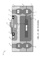
- first and second devices 10 and 11 of different operating voltage ratings are formed on a common semiconductor chip having a substrate material 14 , a first epitaxial layer 16 stacking on top of substrate material 14 and a second epitaxial layer 18 stacking on top of the first epitaxial layer 16 .
- the epitaxial layer 16 is doped to substantially the same concentration as the substrate material 14 .
- Substrate 14 and epitaxial layer 16 are preferably p-type.
- the second epitaxial layer 18 formed on epitaxial layer 16 is preferably n-type. Layers 16 and 18 define a layer stack 12 .
- Active region 20 of device 10 is formed in the n-type epitaxial layer 18 .
- a number of N-wells 22 and P-wells 26 and 48 are provided in the N-Epi layer.
- a greater concentration of n-type dopant is present in wells 22 than is present in layer 18
- P-type well 26 is present in a greater doping concentration than are present in epitaxial layer 16 and substrate 14 .
- a buried region of n-type dopant referred to as a buried region 35 , extends between p-epitaxial layer 16 and n-epitaxial layer having a controlled vertical space 47 less than the thickness of epitaxial layer 18 between the bottom of P-well 26 and the top of buried N region 35 .
- the buried N region 35 is limited to a vicinity around the interface between p-epitaxial layer 16 and n-epitaxial layer 18 such that a substantially greater concentration of n-type dopant is present in buried region 35 than is present in layer 18 .
- isolation regions 40 Disposed on opposing sides of active region 20 and buried region 35 are isolation regions 40 .
- Isolation regions 40 are formed from a plurality of regions having p-type dopant concentrated therein in quantities greater than are present in either substrate 14 or epitaxial layer 16 .
- each of isolation regions 40 comprises of a high voltage P well (HVPW) 48 located at a top portion of the n-type epitaxial layer 18 and overlaps a buried region of p-type buried regions 46 extending between n-type epitaxial layer 18 to the p-type epitaxial layer 16
- HVPW high voltage P well
- Device 10 is identical to the device 300 shown in FIG. 1 , except that device 10 has an additional epitaxial layer 16 formed on top of the substrate.
- the performance of device 10 is identical to the device 300 as the epitaxial layer 16 can be considered as an extension of substrate material 14 .
- the existing manufacturing process and conditions of making device 300 can be transferred in whole as a process module of making device 10 .
- Device 11 includes, formed into layer 18 , an active region 120 . Without showing the detail structure of device 11 , a number of N-wells 122 and P-wells 126 and 148 are provided in the N-Epi layer 18 . A greater concentration of n-type dopant is present in welts 122 than is present in regions of layer 18 outside of wells 122 . P-type dopant of well 126 may be present in a greater concentration than are present in layer 16 and substrate 14 . A deep buried region of n-type dopant, referred to as a deep buried region 134 , extends between substrate 14 and layer stack 12 .
- Deep buried region 134 has two different species, which includes a highly doped first n-type portion, referred to as deep buried highly doped region 136 and a lightly doped second n-type portion, referred to as deep buried lightly doped region 134 with second portion 134 surrounding the first portion 136 .
- highly doped first n-type portion 136 is limited to a vicinity around the interface between the substrate material 14 and the p-epitaxial layer 16 such that a substantially greater concentration of n-type dopant is present in highly doped first n-type portion 136 than is present in layer 16 .
- the second n-type portion extending upward reaches the second epitaxial layer 18 and preferably has a doping concentration substantially the same as layer 18 .
- the second n-type dopant in portion 134 diffuses at a faster rate than the first n-type dopant in portion 136 .
- the dopant concentrated in region 136 is antimony or arsenic and the dopant concentrated in region 138 is phosphorous.
- isolation regions 140 Disposed on opposing sides of active region 120 and deep buried region 134 are isolation regions 140 .
- Isolation regions 140 are formed from a plurality of regions having p-type dopant concentrated therein in quantities greater than are present in either substrate 14 or layer 16 of layer stack 12 .
- isolation regions 140 are each comprised of three overlapping regions 144 , 146 and 148 of p-type doping concentrations.
- a first buried region 144 extends between substrate 14 and first layer 16 .
- a second buried region 146 overlaps with buried region 144 and extends between first epitaxial layer 16 and second epitaxial layer 18 .
- a third well 148 overlaps with the second buried region 146 and extends from surface 50 of second layer 18 toward first layer 16 .
- isolation regions 140 function to isolate active region 120 from adjacent device active regions, one of which is shown as active region 20 formed on substrate 14 and in layer stack 12 .
- a lateral breakdown voltage inside active region 120 is controlled by the lateral distance 52 between regions 134 and 136 and isolation regions 140 and doping concentrations and profiles of regions 134 , 136 , 14 , 16 and 140 .
- a vertical breakdown voltage inside active region 120 is controlled by a vertical distance 51 between region 136 and region 126 and doping concentrations and profiles of regions 134 , 136 , 18 and 126 .
- the second lateral breakdown voltage can be easily increased much higher than the vertical breakdown voltage by placing isolation regions 140 apart from active device region 120 . Therefore, the maximum operating voltage of device 120 is limited by the third vertical breakdown.
- Deep buried regions 100 and 101 are formed in the high voltage device area on top surface thereof the substrate 14 at step 200 , shown in FIGS. 3-6 .
- the dopant is implanted using well known implantation and masking processes to obtain a desired doping concentration.
- deep buried region 101 includes two different types of n-type dopant that have different rates of diffusion coefficient for a given temperature.
- the first n-type dopant is antimony or arsenic and the second dopant is phosphorous, both of which are implanted into a same deep buried region 101 on substrate 14 with two step implantation.
- Deep buried regions 100 include a concentration of p-type dopant.
- the low voltage device area is covered by photo resist to block the ion implant in this step.
- epitaxial layer 16 is grown upon the substrate 14 at step 202 all over the areas.
- Epitaxial layer 16 preferably has the same p-type dopant and same doping concentration as substrate 14 .
- buried regions 104 shown in FIG. 8 , are formed on epitaxial layer 16 and on top of the deep buried regions 100 in the higher operating voltage area.
- buried regions 90 and 92 are formed in the epitaxial layer 16 in furtherance of forming lower operating voltage device 10 . Buried regions 90 and 104 include p-type dopant, and buried region 92 includes n-type dopant.
- the doping concentration in regions 90 and 104 are greater than the doping concentration in the remaining regions of layer 16 .
- This is followed by a thermal anneal that results in the dopants in deep buried regions 100 and 101 , shown in FIG. 7 , diffusing into both substrate and the first epitaxial layer 16 , forming regions 107 , 108 and 109 , shown in FIG. 8 .
- the difference in the diffusion coefficient between antimony and phosphorous, i.e. phosphorous diffuses faster than antimony results in region 109 surrounding region 108 , as discussed above.
- epitaxial layer 18 is grown upon layer 16 , at step 206 .
- Epitaxial layer 18 includes n-type dopant.
- active regions of p-type dopant are implanted into sub-regions 114 , 118 , 214 and 218 into epitaxial layer 18 , followed by implantation of n-type dopant into sub-regions 116 and 216 .
- thermal cycles are applied to drive the dopants into layer 18 sufficiently to provide the desired doping concentrations and profiles.
- Buried region 34 is formed by diffusion of dopant in region 92 .
- Deep buried region 134 and 136 are formed by diffusion of dopants in regions 108 and 109 , respectively.
- Lightly doped phosphorous in region 109 expands upward and converts p-type epitaxial layer 16 to lightly doped n-type, which has similar doping concentration to that of epitaxial layer 18 .
- Isolation regions 40 are formed by the diffusion of dopant in regions 90 .
- Isolation region 140 is formed by merging the diffused dopant in regions 107 , 104 and 214 .
- buried region 34 , deep buried region 134 including highly doped buried region 136 and lightly doped buried region 134 isolation regions 40 and 140 ; and active regions 20 and 120 are formed.
- n-type region 134 converted in p-type epitaxial layer 16 functions as if n-type epitaxial layer 18 is extended downward, therefore, the effective vertical distance 51 between region 136 and region 126 is wider compared to the vertical distance 47 between region 35 and region 26 .
- the device 120 has higher vertical breakdown voltage, hence, higher operating voltage than that of device 20 .
- active region of device 10 is formed by dopant being implanted into N-well regions 116 and P-well region 118 to configure the specific device structure of device 10 and active region of device 11 is formed by dopant being implanted into N-well regions 216 and P-well region 218 to configure specific device structure of device 11 .
- implantation of n-type and p-type dopants at step 208 occurs in multiple steps under conventional implantation and masking processes.
- the proven process and conditions of making device 300 can be transferred in its entirety and implemented starting from step 204 . It should be understood that both existing devices and newly added devices of the present invention having lower voltage rating and higher voltage rating, respectively, will co-exist on the same substrate material without affecting each other.
- the process step 208 shown in FIG. 10 provides a semiconductor chip having a higher voltage device integrated with a lower voltage device.
- device 10 or 11 can be a diode, a bipolar transistor, a MOSFET or other devices. It is further understood that any device combination can be integrated together without affecting each other using the techniques disclosed by this invention.
- FIG. 11 shows an embodiment of device 11 provided as a high voltage vertical NPN transistor (VNPN) 400 integrated with an existing low voltage device (not shown).
- Device 400 is the same as device 11 except that the active area of device 400 includes a highly doped N+ region 130 disposed in the high voltage P-well 126 .
- VNPN vertical NPN transistor
- the highly doped N+ region 130 , the P-well 126 and the N regions including a portion of the N-Epi layer 18 and deep buried N region 134 below the P-well 126 configures a vertical NPN with N+ region 130 provided as the emitter, P-Well 126 provided as the base and the N regions below the HVPW 126 provided as the collector.
- the P+ regions 128 disposed in HVPW 126 provide contact pickups to the base while the N regions 122 disposed in top portion of the N-Epi layer outside of the HVPW 126 provide contact pickups to the collector,
- highly doped N+ regions may be disposed therein to improve ohmic contact to metals electrodes (not shown).
- the base and collector contact pickups may be formed as ring shapes in layout.
- FIG. 12 shows an alternate embodiment of device 11 provided as a high voltage lateral PNP transistor (LPNP) 410 integrated with an existing low voltage device (not shown).
- Device 410 is the same as device 11 except that the active area of device 410 is configured as a lateral PNP including a P region 127 provided as the emitter, a P ring 125 provided as the collector encircling the central P emitter region 127 , and a N ring 123 provided as base contact pickup encircling the collector P ring 125 and the emitter P region 127 .
- the base region includes a portion of the N-Epi layer 18 and the deep buried N region 134 , which further includes the deep buried highly doped region 136 enclosed within a lightly doped buried region 134 .
- the distance 51 between a bottom of the P collector region 125 and a top of the deep buried highly doped region 136 controls the vertical breakdown of the PNP transistor therefore limits the operating voltage of the PNP transistor 410 .
- FIG. 13 shows an alternate embodiment of device 11 provided as a high voltage PN diode 420 integrated with an existing low voltage device (not shown).
- Device 420 is the same as device 11 except that the active area of device 420 is configured as a PN diode including a P region 162 provided as the anode and an N region 160 as contact pickup for the cathode that includes a portion of the N-Epi layer 18 and the deep buried region 134 .
- the distance 51 between a bottom of the anode P region 162 and a top of the deep buried highly doped region 136 controls the vertical breakdown of the diode therefore limits the operating voltage of the diode 420 .
- FIG. 14 shows an alternate embodiment of device 11 provided as a high voltage N-channel Lateral DMOS (LDMOS) integrated with an existing low voltage device (not shown).
- Device 430 is the same as device 11 except that the active area of device 430 is configured as a N-channel LDMOS that includes a N+ source region 157 disposed in P-well 156 and a N+ drain contact pickup region 155 disposed in N-well 154 .
- the P-well 156 is provided as the body and an N region including the N-well 154 , a portion of the N-Epi layer 18 and the deep buried region 134 is provided as the drain.
- a field oxide 152 is formed on a top portion of the N-well 154 right next to the drain contact pickup region 155 and an insulated gate 150 disposed on top of the P-well 156 and the N-well 154 extends from overlapping a portion of the source region 157 to overlapping a portion of the field oxide 152 .
- a P-channel LDMOS 440 can be formed in a same way as shown in FIG. 15 , except that the P+ source region 175 is now disposed in N-well 174 provided as the body and P+ drain contact pickup 177 is now disposed in P-well 176 provided as the drain.
- FIG. 16 shows an alternate embodiment of device 11 provided as a very high voltage N-channel Lateral DMOS (LDMOS) integrated with an existing low voltage device (not shown).
- Device 450 is the same as device 430 except that a RESURF region 137 is provided as a deep P-well (DPW) on a top portion of the deep lightly doped N buried region 134 .
- the DPW region 137 depletes under reverse bias therefore functions as triple RESURF, thus, improves performance of previously described device 430 .
- the DPW region 137 can be formed in the process around the step of 204 by implanting a P type dopant on a top portion of the P-Epi layer 16 in the high voltage device area at the same time or after regions 104 and 106 in FIG.
- the floating DPW region 137 is limited to a vicinity around the interface between p-epitaxial layer 16 and n-epitaxial layer 18 .
- This invention further discloses a method to make a device of increasing operating voltage over an existing device of same functionality by adding a few steps in the early manufacturing process of the existing device therefore without drastically affecting the device performance.
- a first epitaxial layer 16 of the first conductivity type is disposed on the substrate material 14 .
- the epitaxial layer 18 is then disposed on top of the substrate material 14 .
- first epitaxial layer 16 may be different from that of the substrate material 14 .
- the device shown in FIGS. 11-16 may be provided with improved operating voltage following the rest of standard processes and conditions.
Landscapes
- Metal-Oxide And Bipolar Metal-Oxide Semiconductor Integrated Circuits (AREA)
- Insulated Gate Type Field-Effect Transistor (AREA)
Abstract
Description
Claims (16)
Priority Applications (9)
| Application Number | Priority Date | Filing Date | Title |
|---|---|---|---|
| US13/237,842 US9214457B2 (en) | 2011-09-20 | 2011-09-20 | Method of integrating high voltage devices |
| US13/539,360 US20130069157A1 (en) | 2011-09-20 | 2012-06-30 | Semiconductor chip integrating high and low voltage devices |
| US13/539,339 US20130071994A1 (en) | 2011-09-20 | 2012-06-30 | Method of integrating high voltage devices |
| TW101134268A TWI493687B (en) | 2011-09-20 | 2012-09-19 | Method of combining high voltage components |
| CN201210348709.1A CN103021958B (en) | 2011-09-20 | 2012-09-19 | The method of integrated high voltage device |
| US14/633,785 US9793153B2 (en) | 2011-09-20 | 2015-02-27 | Low cost and mask reduction method for high voltage devices |
| US14/968,679 US10157984B2 (en) | 2011-09-20 | 2015-12-14 | Semiconductor device integrating high and low voltage devices |
| US16/191,070 US10770543B2 (en) | 2011-09-20 | 2018-11-14 | Semiconductor chip integrating high and low voltage devices |
| US16/998,924 US11239312B2 (en) | 2011-09-20 | 2020-08-20 | Semiconductor chip integrating high and low voltage devices |
Applications Claiming Priority (1)
| Application Number | Priority Date | Filing Date | Title |
|---|---|---|---|
| US13/237,842 US9214457B2 (en) | 2011-09-20 | 2011-09-20 | Method of integrating high voltage devices |
Related Parent Applications (1)
| Application Number | Title | Priority Date | Filing Date |
|---|---|---|---|
| US13/237,852 Continuation-In-Part US20130069154A1 (en) | 2011-09-20 | 2011-09-20 | Semiconductor chip integrating high and low voltage devices |
Related Child Applications (4)
| Application Number | Title | Priority Date | Filing Date |
|---|---|---|---|
| US13/539,360 Continuation-In-Part US20130069157A1 (en) | 2011-09-20 | 2012-06-30 | Semiconductor chip integrating high and low voltage devices |
| US13/539,339 Continuation-In-Part US20130071994A1 (en) | 2011-09-20 | 2012-06-30 | Method of integrating high voltage devices |
| US14/633,785 Continuation-In-Part US9793153B2 (en) | 2011-09-20 | 2015-02-27 | Low cost and mask reduction method for high voltage devices |
| US14/968,679 Continuation US10157984B2 (en) | 2011-09-20 | 2015-12-14 | Semiconductor device integrating high and low voltage devices |
Publications (2)
| Publication Number | Publication Date |
|---|---|
| US20130072004A1 US20130072004A1 (en) | 2013-03-21 |
| US9214457B2 true US9214457B2 (en) | 2015-12-15 |
Family
ID=47881046
Family Applications (4)
| Application Number | Title | Priority Date | Filing Date |
|---|---|---|---|
| US13/237,842 Active 2031-09-24 US9214457B2 (en) | 2011-09-20 | 2011-09-20 | Method of integrating high voltage devices |
| US14/968,679 Active US10157984B2 (en) | 2011-09-20 | 2015-12-14 | Semiconductor device integrating high and low voltage devices |
| US16/191,070 Active US10770543B2 (en) | 2011-09-20 | 2018-11-14 | Semiconductor chip integrating high and low voltage devices |
| US16/998,924 Active US11239312B2 (en) | 2011-09-20 | 2020-08-20 | Semiconductor chip integrating high and low voltage devices |
Family Applications After (3)
| Application Number | Title | Priority Date | Filing Date |
|---|---|---|---|
| US14/968,679 Active US10157984B2 (en) | 2011-09-20 | 2015-12-14 | Semiconductor device integrating high and low voltage devices |
| US16/191,070 Active US10770543B2 (en) | 2011-09-20 | 2018-11-14 | Semiconductor chip integrating high and low voltage devices |
| US16/998,924 Active US11239312B2 (en) | 2011-09-20 | 2020-08-20 | Semiconductor chip integrating high and low voltage devices |
Country Status (3)
| Country | Link |
|---|---|
| US (4) | US9214457B2 (en) |
| CN (1) | CN103021958B (en) |
| TW (1) | TWI493687B (en) |
Cited By (4)
| Publication number | Priority date | Publication date | Assignee | Title |
|---|---|---|---|---|
| US9460926B2 (en) | 2014-06-30 | 2016-10-04 | Alpha And Omega Semiconductor Incorporated | Forming JFET and LDMOS transistor in monolithic power integrated circuit using deep diffusion regions |
| US20160293758A1 (en) * | 2015-04-03 | 2016-10-06 | Magnachip Semiconductor, Ltd. | Semiconductor structure having a junction field effect transistor and a high voltage transistor and method for manufacturing the same |
| US20190013403A1 (en) * | 2015-04-03 | 2019-01-10 | Magnachip Semiconductor, Ltd. | Semiconductor device with high voltage field effect transistor and junction field effect transistor |
| US10770543B2 (en) | 2011-09-20 | 2020-09-08 | Alpha And Omega Semiconductor Incorporated | Semiconductor chip integrating high and low voltage devices |
Families Citing this family (27)
| Publication number | Priority date | Publication date | Assignee | Title |
|---|---|---|---|---|
| US9793153B2 (en) * | 2011-09-20 | 2017-10-17 | Alpha And Omega Semiconductor Incorporated | Low cost and mask reduction method for high voltage devices |
| CN102664161B (en) * | 2012-05-25 | 2016-11-16 | 杭州士兰集成电路有限公司 | The isolation structure of High voltage BCD process mesohigh device and manufacture method thereof |
| CN103325735A (en) * | 2013-04-24 | 2013-09-25 | 苏州硅智源微电子有限公司 | Method for forming diffusion resistance in integrated circuit isolation region |
| CN103681513B (en) * | 2013-12-20 | 2016-04-13 | 上海岭芯微电子有限公司 | Integrated circuit charging driver and manufacture method thereof |
| US9853119B2 (en) * | 2014-01-31 | 2017-12-26 | Bourns, Inc. | Integration of an auxiliary device with a clamping device in a transient voltage suppressor |
| US9306034B2 (en) | 2014-02-24 | 2016-04-05 | Vanguard International Semiconductor Corporation | Method and apparatus for power device with multiple doped regions |
| KR102177257B1 (en) | 2014-04-15 | 2020-11-10 | 삼성전자주식회사 | Semiconductor device and method for manufacturing the same |
| US10134871B2 (en) * | 2014-12-23 | 2018-11-20 | Taiwan Semiconductor Manufacturing Company, Ltd. | Doping of high-K dielectric oxide by wet chemical treatment |
| US9543292B2 (en) * | 2015-02-27 | 2017-01-10 | Alpha And Omega Semiconductor Incorporated | Field effect transistor with integrated Zener diode |
| CN106328507B (en) * | 2015-06-17 | 2020-09-15 | 联华电子股份有限公司 | Semiconductor device and method of making the same |
| US10381342B2 (en) * | 2015-10-01 | 2019-08-13 | Texas Instruments Incorporated | High voltage bipolar structure for improved pulse width scalability |
| US9831305B1 (en) | 2016-05-06 | 2017-11-28 | Vanguard International Semiconductor Corporation | Semiconductor device and method for manufacturing the same |
| EP3255680A1 (en) * | 2016-06-08 | 2017-12-13 | Vanguard International Semiconductor Corporation | Semiconductor device and method for manufacturing the same |
| TWI613712B (en) * | 2016-12-23 | 2018-02-01 | Nuvoton Technology Corporation | Semiconductor device and method of manufacturing same |
| US10177044B2 (en) * | 2017-05-05 | 2019-01-08 | Newport Fab, Llc | Bulk CMOS RF switch with reduced parasitic capacitance |
| JP7092129B2 (en) * | 2017-07-04 | 2022-06-28 | 住友電気工業株式会社 | Silicon carbide semiconductor device |
| TWI628792B (en) * | 2017-09-21 | 2018-07-01 | Nuvoton Technology Corporation | Semiconductor substrate structure and semiconductor device |
| CN110349929A (en) * | 2018-04-02 | 2019-10-18 | 世界先进积体电路股份有限公司 | High voltage semiconductor device and its manufacturing method |
| TWI673869B (en) | 2018-07-31 | 2019-10-01 | 新唐科技股份有限公司 | High voltage semiconductor devices and methods for manufacturing the same |
| CN109148444B (en) * | 2018-08-22 | 2020-10-27 | 电子科技大学 | BCD semiconductor device and method of manufacturing the same |
| CN111584615A (en) * | 2020-05-09 | 2020-08-25 | 杰华特微电子(杭州)有限公司 | Semiconductor device and related fabrication method |
| CN114530412B (en) * | 2022-01-24 | 2025-09-12 | 华为数字能源技术有限公司 | Device isolation structure and manufacturing method thereof, and semiconductor device |
| US12532537B2 (en) * | 2022-08-03 | 2026-01-20 | Vanguard International Semiconductor Corporation | Semiconductor device with a deep trench isolation structure and buried layers for reducing substrate leakage current and avoiding latch-up effect, and fabrication method thereof |
| EP4354496B1 (en) * | 2022-10-13 | 2025-05-14 | Nxp B.V. | Isolation structure for an active component |
| CN115799158A (en) * | 2022-10-28 | 2023-03-14 | 上海华虹宏力半导体制造有限公司 | Semiconductor structures and methods of forming them |
| TWI856473B (en) * | 2023-01-04 | 2024-09-21 | 世界先進積體電路股份有限公司 | Semiconductor device |
| CN116314264A (en) * | 2023-03-01 | 2023-06-23 | 绍兴中芯集成电路制造股份有限公司 | Level shifter, manufacturing method thereof, and semiconductor device |
Citations (67)
| Publication number | Priority date | Publication date | Assignee | Title |
|---|---|---|---|---|
| US3335341A (en) | 1964-03-06 | 1967-08-08 | Westinghouse Electric Corp | Diode structure in semiconductor integrated circuit and method of making the same |
| US3466510A (en) * | 1967-01-07 | 1969-09-09 | Telefunken Patent | Integrated graetz rectifier circuit |
| US4300150A (en) | 1980-06-16 | 1981-11-10 | North American Philips Corporation | Lateral double-diffused MOS transistor device |
| US4458158A (en) * | 1979-03-12 | 1984-07-03 | Sprague Electric Company | IC Including small signal and power devices |
| US4665424A (en) * | 1984-03-30 | 1987-05-12 | Mitsubishi Denki Kabushiki Kaisha | Semiconductor device |
| US4697332A (en) | 1984-05-25 | 1987-10-06 | Gould Inc. | Method of making tri-well CMOS by self-aligned process |
| US4800172A (en) | 1987-02-09 | 1989-01-24 | Kabushiki Kaisha Toshiba | Manufacturing method for cascaded junction field effect transistor |
| US4887142A (en) | 1986-01-30 | 1989-12-12 | Sgs Microelettronica S.P.A. | Monolithically integrated semiconductor device containing bipolar junction transistors, CMOS and DMOS transistors and low leakage diodes and a method for its fabrication |
| US4890146A (en) * | 1987-12-16 | 1989-12-26 | Siliconix Incorporated | High voltage level shift semiconductor device |
| US4918026A (en) | 1989-03-17 | 1990-04-17 | Delco Electronics Corporation | Process for forming vertical bipolar transistors and high voltage CMOS in a single integrated circuit chip |
| US4979001A (en) | 1989-06-30 | 1990-12-18 | Micrel Incorporated | Hidden zener diode structure in configurable integrated circuit |
| US5041895A (en) | 1989-06-14 | 1991-08-20 | Sgs-Thomson Microelectronics S.R.L. | Mixed technology integrated device comprising complementary LDMOS power transistors, CMOS and vertical PNP integrated structures having an enhanced ability to withstand a relatively high supply voltage |
| US5047820A (en) | 1988-09-14 | 1991-09-10 | Micrel, Inc. | Semi self-aligned high voltage P channel FET |
| US5087889A (en) | 1991-02-20 | 1992-02-11 | Analog Devices, Inc. | Area efficient cascode driver circuit |
| US5094963A (en) * | 1981-07-17 | 1992-03-10 | Fujitsu Limited | Process for producing a semiconductor device with a bulk-defect region having a nonuniform depth |
| US5156989A (en) * | 1988-11-08 | 1992-10-20 | Siliconix, Incorporated | Complementary, isolated DMOS IC technology |
| US5158463A (en) | 1991-04-09 | 1992-10-27 | Samsung Electronics Co., Ltd. | Method of manufacturing both low and high voltage BiCMOS transistors in the same semiconductor substrate |
| US5225359A (en) | 1990-08-17 | 1993-07-06 | National Semiconductor Corporation | Method of fabricating Schottky barrier diodes and Schottky barrier diode-clamped transistors |
| US5242841A (en) | 1992-03-25 | 1993-09-07 | Texas Instruments Incorporated | Method of making LDMOS transistor with self-aligned source/backgate and photo-aligned gate |
| US5273912A (en) * | 1991-08-12 | 1993-12-28 | Sharp Kabushiki Kaisha | Method for manufacturing semiconductor device |
| US5286995A (en) | 1992-07-14 | 1994-02-15 | Texas Instruments Incorporated | Isolated resurf LDMOS devices for multiple outputs on one die |
| US5296393A (en) | 1990-11-23 | 1994-03-22 | Texas Instruments Incorporated | Process for the simultaneous fabrication of high-and-low-voltage semiconductor devices, integrated circuit containing the same, systems and methods |
| US5338949A (en) | 1992-04-14 | 1994-08-16 | U.S. Philips Corporation | Semiconductor device having series-connected junction field effect transistors |
| US5355014A (en) | 1993-03-03 | 1994-10-11 | Bhasker Rao | Semiconductor device with integrated RC network and Schottky diode |
| US5387552A (en) | 1991-03-22 | 1995-02-07 | National Semiconductor Corporation | Method of fabrication of PNP structure in a common substrate containing NPN or MOS structures |
| US5406110A (en) | 1991-12-30 | 1995-04-11 | Texas Instruments Incorporated | Resurf lateral double diffused insulated gate field effect transistor |
| US5408125A (en) * | 1989-09-25 | 1995-04-18 | Texas Instruments Incorporated | Semiconductor process for manufacturing semiconductor device with increased operating voltages |
| US5498554A (en) | 1994-04-08 | 1996-03-12 | Texas Instruments Incorporated | Method of making extended drain resurf lateral DMOS devices |
| US5517046A (en) | 1993-11-19 | 1996-05-14 | Micrel, Incorporated | High voltage lateral DMOS device with enhanced drift region |
| US5539237A (en) | 1993-01-21 | 1996-07-23 | Texas Instruments Incorporated | Schottky diode with guard ring |
| US5545577A (en) | 1992-04-30 | 1996-08-13 | Fuji Electric Co., Ltd. | Method of producing a semiconductor device having two MIS transistor circuits |
| US5556796A (en) | 1995-04-25 | 1996-09-17 | Micrel, Inc. | Self-alignment technique for forming junction isolation and wells |
| US5578855A (en) * | 1994-02-15 | 1996-11-26 | National Semiconductor Corporation | High-voltage CMOS transistors on a standard CMOS wafer |
| US5610421A (en) | 1993-12-15 | 1997-03-11 | Sgs-Thomson Microelectronics S.R.L. | Integrated circuit with EPROM cells |
| US5614755A (en) * | 1993-04-30 | 1997-03-25 | Texas Instruments Incorporated | High voltage Shottky diode |
| US5698457A (en) | 1995-02-28 | 1997-12-16 | Nec Corporation | Method for manufacturing high voltage semiconductor device |
| US5736445A (en) | 1995-07-18 | 1998-04-07 | Siemens Aktiengesellschaft | Method for producing at least two transsistors in a semiconductor body |
| US5750414A (en) | 1993-09-29 | 1998-05-12 | Siemens Components, Inc. | Method of fabricating a semiconductor device |
| US5854566A (en) | 1995-10-13 | 1998-12-29 | Lg Semicon Co., Ltd. | RESURF EDMOS transistor and high-voltage analog multiplexer circuit using the same |
| US5856695A (en) | 1991-10-30 | 1999-01-05 | Harris Corporation | BiCMOS devices |
| US5911104A (en) | 1998-02-20 | 1999-06-08 | Texas Instruments Incorporated | Integrated circuit combining high frequency bipolar and high power CMOS transistors |
| US5913114A (en) | 1997-01-23 | 1999-06-15 | Samsung Electronics Co., Ltd. | Method of manufacturing a semiconductor device |
| US6096589A (en) | 1996-09-06 | 2000-08-01 | Micron Technology, Inc. | Low and high voltage CMOS devices and process for fabricating same |
| US6127213A (en) | 1999-04-14 | 2000-10-03 | United Microelectronics Corp. | Method for simultaneously forming low voltage and high voltage devices |
| US6207510B1 (en) | 1999-01-12 | 2001-03-27 | Lucent Technologies Inc. | Method for making an integrated circuit including high and low voltage transistors |
| US6211552B1 (en) | 1999-05-27 | 2001-04-03 | Texas Instruments Incorporated | Resurf LDMOS device with deep drain region |
| US6242787B1 (en) | 1995-11-15 | 2001-06-05 | Denso Corporation | Semiconductor device and manufacturing method thereof |
| US6306700B1 (en) | 2000-08-07 | 2001-10-23 | United Microelectronics Corp. | Method for forming high voltage devices compatible with low voltages devices on semiconductor substrate |
| USRE37424E1 (en) * | 1989-06-14 | 2001-10-30 | Stmicroelectronics S.R.L. | Mixed technology integrated device comprising complementary LDMOS power transistors, CMOS and vertical PNP integrated structures having an enhanced ability to withstand a relatively high supply voltage |
| US6352887B1 (en) | 1998-03-26 | 2002-03-05 | Texas Instruments Incorporated | Merged bipolar and CMOS circuit and method |
| US6365447B1 (en) * | 1998-01-12 | 2002-04-02 | National Semiconductor Corporation | High-voltage complementary bipolar and BiCMOS technology using double expitaxial growth |
| US6410377B1 (en) | 2000-11-06 | 2002-06-25 | Ching-Chun Hwang | Method for integrating CMOS sensor and high voltage device |
| US6525376B1 (en) | 1998-01-26 | 2003-02-25 | Seiko Instruments Inc. | High withstand voltage insulated gate N-channel field effect transistor |
| US6593621B2 (en) | 2001-08-23 | 2003-07-15 | Micrel, Inc. | LDMOS field effect transistor with improved ruggedness in narrow curved areas |
| US6818494B1 (en) | 2001-03-26 | 2004-11-16 | Hewlett-Packard Development Company, L.P. | LDMOS and CMOS integrated circuit and method of making |
| US6833586B2 (en) | 2003-01-02 | 2004-12-21 | Micrel, Inc. | LDMOS transistor with high voltage source and drain terminals |
| US6844578B2 (en) | 2001-03-28 | 2005-01-18 | Seiko Instruments Inc. | Semiconductor integrated circuit device and manufacturing method therefor |
| US6894349B2 (en) | 2001-06-08 | 2005-05-17 | Intersil Americas Inc. | Lateral DMOS structure with lateral extension structure for reduced charge trapping in gate oxide |
| US6900091B2 (en) | 2002-08-14 | 2005-05-31 | Advanced Analogic Technologies, Inc. | Isolated complementary MOS devices in epi-less substrate |
| US20050253216A1 (en) | 2002-12-17 | 2005-11-17 | Hideaki Tsuchiko | Integrated circuit including a high voltage LDMOS device and low voltage devices |
| US6995453B2 (en) | 2002-03-09 | 2006-02-07 | Fairchild Korea Semiconductor Ltd. | High voltage integrated circuit including bipolar transistor within high voltage island area |
| US7166893B2 (en) | 1998-12-25 | 2007-01-23 | Renesas Technology Corp. | Semiconductor integrated circuit device |
| US7291884B2 (en) * | 2001-07-03 | 2007-11-06 | Siliconix Incorporated | Trench MIS device having implanted drain-drift region and thick bottom oxide |
| US7514754B2 (en) * | 2007-01-19 | 2009-04-07 | Episil Technologies Inc. | Complementary metal-oxide-semiconductor transistor for avoiding a latch-up problem |
| US7619299B2 (en) * | 2005-11-30 | 2009-11-17 | Sanyo Electric Co., Ltd. | Semiconductor device and method of manufacturing the same |
| US7719055B1 (en) | 2007-05-10 | 2010-05-18 | Northrop Grumman Systems Corporation | Cascode power switch topologies |
| US20110079825A1 (en) | 2006-01-24 | 2011-04-07 | Alpha And Omega Semiconductor Incorporated | Cascoded high voltage junction field effect transistor |
Family Cites Families (18)
| Publication number | Priority date | Publication date | Assignee | Title |
|---|---|---|---|---|
| US3911470A (en) * | 1970-11-14 | 1975-10-07 | Philips Corp | Integrated circuit for logic purposes having transistors with different base thicknesses and method of manufacturing |
| JPS55153365A (en) * | 1979-05-17 | 1980-11-29 | Toshiba Corp | Manufacturing method of semiconductor device |
| JPS61154063A (en) * | 1984-12-26 | 1986-07-12 | Toshiba Corp | Optical semiconductor device and manufacture thereof |
| IT1218128B (en) * | 1987-03-05 | 1990-04-12 | Sgs Microelettronica Spa | INTEGRATED STRUCTURE FOR SIGNAL TRANSFER NETWORK, ESPECIALLY FOR PILOT CIRCUIT FOR POWER MOS TRANSISTORS |
| US5153697A (en) * | 1989-02-10 | 1992-10-06 | Texas Instruments Incorporated | Integrated circuit that combines multi-epitaxial power transistors with logic/analog devices, and a process to produce same |
| IT1228900B (en) * | 1989-02-27 | 1991-07-09 | Sgs Thomson Microelectronics | INTEGRATED MONOLITHIC STRUCTURE FOR TWO-STAGE PILOTING SYSTEM WITH CIRCUIT COMPONENT LEVEL TRANSLATOR OF THE PILOT SIGNAL FOR POWER TRANSISTORS. |
| US5248624A (en) * | 1991-08-23 | 1993-09-28 | Exar Corporation | Method of making isolated vertical pnp transistor in a complementary bicmos process with eeprom memory |
| US6150200A (en) * | 1998-04-03 | 2000-11-21 | Motorola, Inc. | Semiconductor device and method of making |
| KR20000014215A (en) | 1998-08-18 | 2000-03-06 | 김덕중 | Method for manufacturing the reliable lateral transistor |
| IT1311309B1 (en) * | 1999-12-10 | 2002-03-12 | St Microelectronics Srl | HIGH VOLTAGE INTEGRATED VERTICAL RESISTOR AND RELATED MANUFACTURING PROCESS. |
| US6855985B2 (en) | 2002-09-29 | 2005-02-15 | Advanced Analogic Technologies, Inc. | Modular bipolar-CMOS-DMOS analog integrated circuit & power transistor technology |
| WO2007052196A1 (en) * | 2005-11-02 | 2007-05-10 | Nxp B.V. | Method of manufacturing a semiconductor device |
| CN101459142A (en) * | 2007-12-11 | 2009-06-17 | 上海华虹Nec电子有限公司 | Method for growing high voltage and low voltage devices in E2PROM |
| CN101599462B (en) * | 2009-06-13 | 2011-02-16 | 无锡中微爱芯电子有限公司 | Production method of high and low voltage devices based on thin epitaxy |
| US8237223B2 (en) * | 2009-09-10 | 2012-08-07 | Episil Technologies Inc. | Semiconductor device |
| CN101714552B (en) * | 2009-11-09 | 2011-05-25 | 苏州博创集成电路设计有限公司 | High-low voltage device for plasma display driving chip and preparation method |
| CN102104038B (en) * | 2010-12-23 | 2013-11-20 | 普缘芯半导体科技(上海)有限公司 | Semiconductor device provided with high-voltage and low-voltage components on identical substrate |
| US9214457B2 (en) | 2011-09-20 | 2015-12-15 | Alpha & Omega Semiconductor Incorporated | Method of integrating high voltage devices |
-
2011
- 2011-09-20 US US13/237,842 patent/US9214457B2/en active Active
-
2012
- 2012-09-19 TW TW101134268A patent/TWI493687B/en active
- 2012-09-19 CN CN201210348709.1A patent/CN103021958B/en active Active
-
2015
- 2015-12-14 US US14/968,679 patent/US10157984B2/en active Active
-
2018
- 2018-11-14 US US16/191,070 patent/US10770543B2/en active Active
-
2020
- 2020-08-20 US US16/998,924 patent/US11239312B2/en active Active
Patent Citations (71)
| Publication number | Priority date | Publication date | Assignee | Title |
|---|---|---|---|---|
| US3335341A (en) | 1964-03-06 | 1967-08-08 | Westinghouse Electric Corp | Diode structure in semiconductor integrated circuit and method of making the same |
| US3466510A (en) * | 1967-01-07 | 1969-09-09 | Telefunken Patent | Integrated graetz rectifier circuit |
| US4458158A (en) * | 1979-03-12 | 1984-07-03 | Sprague Electric Company | IC Including small signal and power devices |
| US4300150A (en) | 1980-06-16 | 1981-11-10 | North American Philips Corporation | Lateral double-diffused MOS transistor device |
| US5094963A (en) * | 1981-07-17 | 1992-03-10 | Fujitsu Limited | Process for producing a semiconductor device with a bulk-defect region having a nonuniform depth |
| US4665424A (en) * | 1984-03-30 | 1987-05-12 | Mitsubishi Denki Kabushiki Kaisha | Semiconductor device |
| US4697332A (en) | 1984-05-25 | 1987-10-06 | Gould Inc. | Method of making tri-well CMOS by self-aligned process |
| US4887142A (en) | 1986-01-30 | 1989-12-12 | Sgs Microelettronica S.P.A. | Monolithically integrated semiconductor device containing bipolar junction transistors, CMOS and DMOS transistors and low leakage diodes and a method for its fabrication |
| US4800172A (en) | 1987-02-09 | 1989-01-24 | Kabushiki Kaisha Toshiba | Manufacturing method for cascaded junction field effect transistor |
| US4890146A (en) * | 1987-12-16 | 1989-12-26 | Siliconix Incorporated | High voltage level shift semiconductor device |
| US5047820A (en) | 1988-09-14 | 1991-09-10 | Micrel, Inc. | Semi self-aligned high voltage P channel FET |
| US5156989A (en) * | 1988-11-08 | 1992-10-20 | Siliconix, Incorporated | Complementary, isolated DMOS IC technology |
| US4918026A (en) | 1989-03-17 | 1990-04-17 | Delco Electronics Corporation | Process for forming vertical bipolar transistors and high voltage CMOS in a single integrated circuit chip |
| US5041895A (en) | 1989-06-14 | 1991-08-20 | Sgs-Thomson Microelectronics S.R.L. | Mixed technology integrated device comprising complementary LDMOS power transistors, CMOS and vertical PNP integrated structures having an enhanced ability to withstand a relatively high supply voltage |
| USRE37424E1 (en) * | 1989-06-14 | 2001-10-30 | Stmicroelectronics S.R.L. | Mixed technology integrated device comprising complementary LDMOS power transistors, CMOS and vertical PNP integrated structures having an enhanced ability to withstand a relatively high supply voltage |
| US4979001A (en) | 1989-06-30 | 1990-12-18 | Micrel Incorporated | Hidden zener diode structure in configurable integrated circuit |
| US5408125A (en) * | 1989-09-25 | 1995-04-18 | Texas Instruments Incorporated | Semiconductor process for manufacturing semiconductor device with increased operating voltages |
| US5225359A (en) | 1990-08-17 | 1993-07-06 | National Semiconductor Corporation | Method of fabricating Schottky barrier diodes and Schottky barrier diode-clamped transistors |
| US5296393A (en) | 1990-11-23 | 1994-03-22 | Texas Instruments Incorporated | Process for the simultaneous fabrication of high-and-low-voltage semiconductor devices, integrated circuit containing the same, systems and methods |
| US5087889A (en) | 1991-02-20 | 1992-02-11 | Analog Devices, Inc. | Area efficient cascode driver circuit |
| US5387552A (en) | 1991-03-22 | 1995-02-07 | National Semiconductor Corporation | Method of fabrication of PNP structure in a common substrate containing NPN or MOS structures |
| US5158463A (en) | 1991-04-09 | 1992-10-27 | Samsung Electronics Co., Ltd. | Method of manufacturing both low and high voltage BiCMOS transistors in the same semiconductor substrate |
| US5273912A (en) * | 1991-08-12 | 1993-12-28 | Sharp Kabushiki Kaisha | Method for manufacturing semiconductor device |
| US5856695A (en) | 1991-10-30 | 1999-01-05 | Harris Corporation | BiCMOS devices |
| US5406110A (en) | 1991-12-30 | 1995-04-11 | Texas Instruments Incorporated | Resurf lateral double diffused insulated gate field effect transistor |
| US5242841A (en) | 1992-03-25 | 1993-09-07 | Texas Instruments Incorporated | Method of making LDMOS transistor with self-aligned source/backgate and photo-aligned gate |
| US5338949A (en) | 1992-04-14 | 1994-08-16 | U.S. Philips Corporation | Semiconductor device having series-connected junction field effect transistors |
| US5545577A (en) | 1992-04-30 | 1996-08-13 | Fuji Electric Co., Ltd. | Method of producing a semiconductor device having two MIS transistor circuits |
| US5286995A (en) | 1992-07-14 | 1994-02-15 | Texas Instruments Incorporated | Isolated resurf LDMOS devices for multiple outputs on one die |
| US5539237A (en) | 1993-01-21 | 1996-07-23 | Texas Instruments Incorporated | Schottky diode with guard ring |
| US5355014A (en) | 1993-03-03 | 1994-10-11 | Bhasker Rao | Semiconductor device with integrated RC network and Schottky diode |
| US5614755A (en) * | 1993-04-30 | 1997-03-25 | Texas Instruments Incorporated | High voltage Shottky diode |
| US5750414A (en) | 1993-09-29 | 1998-05-12 | Siemens Components, Inc. | Method of fabricating a semiconductor device |
| US5517046A (en) | 1993-11-19 | 1996-05-14 | Micrel, Incorporated | High voltage lateral DMOS device with enhanced drift region |
| US5610421A (en) | 1993-12-15 | 1997-03-11 | Sgs-Thomson Microelectronics S.R.L. | Integrated circuit with EPROM cells |
| US5578855A (en) * | 1994-02-15 | 1996-11-26 | National Semiconductor Corporation | High-voltage CMOS transistors on a standard CMOS wafer |
| US5789786A (en) * | 1994-02-15 | 1998-08-04 | National Semiconductor Corporation | High-Voltage CMOS transistors on a standard CMOS wafer |
| US5498554A (en) | 1994-04-08 | 1996-03-12 | Texas Instruments Incorporated | Method of making extended drain resurf lateral DMOS devices |
| US5698457A (en) | 1995-02-28 | 1997-12-16 | Nec Corporation | Method for manufacturing high voltage semiconductor device |
| US5556796A (en) | 1995-04-25 | 1996-09-17 | Micrel, Inc. | Self-alignment technique for forming junction isolation and wells |
| US5736445A (en) | 1995-07-18 | 1998-04-07 | Siemens Aktiengesellschaft | Method for producing at least two transsistors in a semiconductor body |
| US5854566A (en) | 1995-10-13 | 1998-12-29 | Lg Semicon Co., Ltd. | RESURF EDMOS transistor and high-voltage analog multiplexer circuit using the same |
| US6242787B1 (en) | 1995-11-15 | 2001-06-05 | Denso Corporation | Semiconductor device and manufacturing method thereof |
| US6096589A (en) | 1996-09-06 | 2000-08-01 | Micron Technology, Inc. | Low and high voltage CMOS devices and process for fabricating same |
| US5913114A (en) | 1997-01-23 | 1999-06-15 | Samsung Electronics Co., Ltd. | Method of manufacturing a semiconductor device |
| US6365447B1 (en) * | 1998-01-12 | 2002-04-02 | National Semiconductor Corporation | High-voltage complementary bipolar and BiCMOS technology using double expitaxial growth |
| US6525376B1 (en) | 1998-01-26 | 2003-02-25 | Seiko Instruments Inc. | High withstand voltage insulated gate N-channel field effect transistor |
| US5911104A (en) | 1998-02-20 | 1999-06-08 | Texas Instruments Incorporated | Integrated circuit combining high frequency bipolar and high power CMOS transistors |
| US6352887B1 (en) | 1998-03-26 | 2002-03-05 | Texas Instruments Incorporated | Merged bipolar and CMOS circuit and method |
| US7166893B2 (en) | 1998-12-25 | 2007-01-23 | Renesas Technology Corp. | Semiconductor integrated circuit device |
| US6207510B1 (en) | 1999-01-12 | 2001-03-27 | Lucent Technologies Inc. | Method for making an integrated circuit including high and low voltage transistors |
| US6127213A (en) | 1999-04-14 | 2000-10-03 | United Microelectronics Corp. | Method for simultaneously forming low voltage and high voltage devices |
| US6211552B1 (en) | 1999-05-27 | 2001-04-03 | Texas Instruments Incorporated | Resurf LDMOS device with deep drain region |
| US6306700B1 (en) | 2000-08-07 | 2001-10-23 | United Microelectronics Corp. | Method for forming high voltage devices compatible with low voltages devices on semiconductor substrate |
| US6410377B1 (en) | 2000-11-06 | 2002-06-25 | Ching-Chun Hwang | Method for integrating CMOS sensor and high voltage device |
| US6818494B1 (en) | 2001-03-26 | 2004-11-16 | Hewlett-Packard Development Company, L.P. | LDMOS and CMOS integrated circuit and method of making |
| US6844578B2 (en) | 2001-03-28 | 2005-01-18 | Seiko Instruments Inc. | Semiconductor integrated circuit device and manufacturing method therefor |
| US6894349B2 (en) | 2001-06-08 | 2005-05-17 | Intersil Americas Inc. | Lateral DMOS structure with lateral extension structure for reduced charge trapping in gate oxide |
| US7435650B2 (en) * | 2001-07-03 | 2008-10-14 | Siliconix Incorporated | Process for manufacturing trench MIS device having implanted drain-drift region and thick bottom oxide |
| US7291884B2 (en) * | 2001-07-03 | 2007-11-06 | Siliconix Incorporated | Trench MIS device having implanted drain-drift region and thick bottom oxide |
| US6593621B2 (en) | 2001-08-23 | 2003-07-15 | Micrel, Inc. | LDMOS field effect transistor with improved ruggedness in narrow curved areas |
| US6995453B2 (en) | 2002-03-09 | 2006-02-07 | Fairchild Korea Semiconductor Ltd. | High voltage integrated circuit including bipolar transistor within high voltage island area |
| US6900091B2 (en) | 2002-08-14 | 2005-05-31 | Advanced Analogic Technologies, Inc. | Isolated complementary MOS devices in epi-less substrate |
| US20050253216A1 (en) | 2002-12-17 | 2005-11-17 | Hideaki Tsuchiko | Integrated circuit including a high voltage LDMOS device and low voltage devices |
| US7019377B2 (en) | 2002-12-17 | 2006-03-28 | Micrel, Inc. | Integrated circuit including high voltage devices and low voltage devices |
| US7759759B2 (en) | 2002-12-17 | 2010-07-20 | Micrel Incorporated | Integrated circuit including a high voltage bipolar device and low voltage devices |
| US6833586B2 (en) | 2003-01-02 | 2004-12-21 | Micrel, Inc. | LDMOS transistor with high voltage source and drain terminals |
| US7619299B2 (en) * | 2005-11-30 | 2009-11-17 | Sanyo Electric Co., Ltd. | Semiconductor device and method of manufacturing the same |
| US20110079825A1 (en) | 2006-01-24 | 2011-04-07 | Alpha And Omega Semiconductor Incorporated | Cascoded high voltage junction field effect transistor |
| US7514754B2 (en) * | 2007-01-19 | 2009-04-07 | Episil Technologies Inc. | Complementary metal-oxide-semiconductor transistor for avoiding a latch-up problem |
| US7719055B1 (en) | 2007-05-10 | 2010-05-18 | Northrop Grumman Systems Corporation | Cascode power switch topologies |
Non-Patent Citations (1)
| Title |
|---|
| U.S. Appl. No. 13/237,852, filed Sep. 20, 2011 and listing Hideaki Tsuchiko as inventor. |
Cited By (10)
| Publication number | Priority date | Publication date | Assignee | Title |
|---|---|---|---|---|
| US10770543B2 (en) | 2011-09-20 | 2020-09-08 | Alpha And Omega Semiconductor Incorporated | Semiconductor chip integrating high and low voltage devices |
| US11239312B2 (en) | 2011-09-20 | 2022-02-01 | Alpha And Omega Semiconductor Incorporated | Semiconductor chip integrating high and low voltage devices |
| US9460926B2 (en) | 2014-06-30 | 2016-10-04 | Alpha And Omega Semiconductor Incorporated | Forming JFET and LDMOS transistor in monolithic power integrated circuit using deep diffusion regions |
| US10109625B2 (en) | 2014-06-30 | 2018-10-23 | Alpha And Omega Semiconductor, Inc. | JFET and LDMOS transistor formed using deep diffusion regions |
| US20160293758A1 (en) * | 2015-04-03 | 2016-10-06 | Magnachip Semiconductor, Ltd. | Semiconductor structure having a junction field effect transistor and a high voltage transistor and method for manufacturing the same |
| US9947786B2 (en) * | 2015-04-03 | 2018-04-17 | Magnachip Semiconductor, Ltd. | Semiconductor structure having a junction field effect transistor and a high voltage transistor and method for manufacturing the same |
| US20180197991A1 (en) * | 2015-04-03 | 2018-07-12 | Magnachip Semiconductor, Ltd. | Semiconductor structure having a junction field effect transistor and a high voltage transistor and method for manufacturing the same |
| US10096707B2 (en) * | 2015-04-03 | 2018-10-09 | Magnachip Semiconductor, Ltd. | Semiconductor structure having a junction field effect transistor and a high voltage transistor and method for manufacturing the same |
| US20190013403A1 (en) * | 2015-04-03 | 2019-01-10 | Magnachip Semiconductor, Ltd. | Semiconductor device with high voltage field effect transistor and junction field effect transistor |
| US10784372B2 (en) * | 2015-04-03 | 2020-09-22 | Magnachip Semiconductor, Ltd. | Semiconductor device with high voltage field effect transistor and junction field effect transistor |
Also Published As
| Publication number | Publication date |
|---|---|
| US20160099310A1 (en) | 2016-04-07 |
| US10157984B2 (en) | 2018-12-18 |
| US10770543B2 (en) | 2020-09-08 |
| CN103021958A (en) | 2013-04-03 |
| CN103021958B (en) | 2015-11-18 |
| US20200381513A1 (en) | 2020-12-03 |
| TWI493687B (en) | 2015-07-21 |
| US20130072004A1 (en) | 2013-03-21 |
| US20190088740A1 (en) | 2019-03-21 |
| US11239312B2 (en) | 2022-02-01 |
| TW201314868A (en) | 2013-04-01 |
Similar Documents
| Publication | Publication Date | Title |
|---|---|---|
| US11239312B2 (en) | Semiconductor chip integrating high and low voltage devices | |
| US20130069154A1 (en) | Semiconductor chip integrating high and low voltage devices | |
| US20130071994A1 (en) | Method of integrating high voltage devices | |
| US6943426B2 (en) | Complementary analog bipolar transistors with trench-constrained isolation diffusion | |
| US7187033B2 (en) | Drain-extended MOS transistors with diode clamp and methods for making the same | |
| KR101303405B1 (en) | Isolated transistors and diodes and isolation and termination structures for semiconductor die | |
| US8278710B2 (en) | Guard ring integrated LDMOS | |
| KR102138385B1 (en) | Low-cost semiconductor device manufacturing method | |
| US7898008B2 (en) | Vertical-type, integrated bipolar device and manufacturing process thereof | |
| TWI588972B (en) | Semiconductor component and preparation method thereof | |
| JP2006514425A5 (en) | ||
| US20130069157A1 (en) | Semiconductor chip integrating high and low voltage devices | |
| CN103515324B (en) | The method of integrated high voltage device | |
| US10224402B2 (en) | Method of improving lateral BJT characteristics in BCD technology | |
| HK1176462B (en) | Isolated transistors and diodes and isolation and termination structures for semiconductor die |
Legal Events
| Date | Code | Title | Description |
|---|---|---|---|
| AS | Assignment |
Owner name: ALPHA AND OMEGA SEMICONDUCTOR INCORPORATED, CALIFO Free format text: ASSIGNMENT OF ASSIGNORS INTEREST;ASSIGNOR:TSUCHIKO, HIDEAKI;REEL/FRAME:026937/0966 Effective date: 20110919 |
|
| STCF | Information on status: patent grant |
Free format text: PATENTED CASE |
|
| MAFP | Maintenance fee payment |
Free format text: PAYMENT OF MAINTENANCE FEE, 4TH YEAR, LARGE ENTITY (ORIGINAL EVENT CODE: M1551); ENTITY STATUS OF PATENT OWNER: LARGE ENTITY Year of fee payment: 4 |
|
| MAFP | Maintenance fee payment |
Free format text: PAYMENT OF MAINTENANCE FEE, 8TH YEAR, LARGE ENTITY (ORIGINAL EVENT CODE: M1552); ENTITY STATUS OF PATENT OWNER: LARGE ENTITY Year of fee payment: 8 |