TWI856473B - Semiconductor device - Google Patents
Semiconductor device Download PDFInfo
- Publication number
- TWI856473B TWI856473B TW112100186A TW112100186A TWI856473B TW I856473 B TWI856473 B TW I856473B TW 112100186 A TW112100186 A TW 112100186A TW 112100186 A TW112100186 A TW 112100186A TW I856473 B TWI856473 B TW I856473B
- Authority
- TW
- Taiwan
- Prior art keywords
- region
- main
- doping
- current spreading
- doped region
- Prior art date
Links
- 239000004065 semiconductor Substances 0.000 title claims abstract description 161
- 238000003892 spreading Methods 0.000 claims abstract description 159
- 239000000758 substrate Substances 0.000 claims abstract description 54
- 238000002955 isolation Methods 0.000 claims abstract description 30
- IDIJOAIHTRIPRC-UHFFFAOYSA-J hexaaluminum;sodium;2,2,4,4,6,6,8,8,10,10,12,12-dodecaoxido-1,3,5,7,9,11-hexaoxa-2,4,6,8,10,12-hexasilacyclododecane;iron(2+);triborate;tetrahydroxide Chemical compound [OH-].[OH-].[OH-].[OH-].[Na+].[Al+3].[Al+3].[Al+3].[Al+3].[Al+3].[Al+3].[Fe+2].[Fe+2].[Fe+2].[O-]B([O-])[O-].[O-]B([O-])[O-].[O-]B([O-])[O-].[O-][Si]1([O-])O[Si]([O-])([O-])O[Si]([O-])([O-])O[Si]([O-])([O-])O[Si]([O-])([O-])O[Si]([O-])([O-])O1 IDIJOAIHTRIPRC-UHFFFAOYSA-J 0.000 claims description 4
- 229910000246 schorl Inorganic materials 0.000 claims description 4
- 238000000034 method Methods 0.000 description 14
- 229910045601 alloy Inorganic materials 0.000 description 8
- 239000000956 alloy Substances 0.000 description 8
- 238000010586 diagram Methods 0.000 description 8
- 239000000463 material Substances 0.000 description 8
- 229910052751 metal Inorganic materials 0.000 description 7
- 239000002184 metal Substances 0.000 description 7
- 230000003647 oxidation Effects 0.000 description 6
- 238000007254 oxidation reaction Methods 0.000 description 6
- PXHVJJICTQNCMI-UHFFFAOYSA-N Nickel Chemical compound [Ni] PXHVJJICTQNCMI-UHFFFAOYSA-N 0.000 description 5
- 230000015556 catabolic process Effects 0.000 description 5
- 239000002019 doping agent Substances 0.000 description 5
- BASFCYQUMIYNBI-UHFFFAOYSA-N platinum Chemical compound [Pt] BASFCYQUMIYNBI-UHFFFAOYSA-N 0.000 description 5
- 125000006850 spacer group Chemical group 0.000 description 5
- JBRZTFJDHDCESZ-UHFFFAOYSA-N AsGa Chemical compound [As]#[Ga] JBRZTFJDHDCESZ-UHFFFAOYSA-N 0.000 description 4
- XUIMIQQOPSSXEZ-UHFFFAOYSA-N Silicon Chemical compound [Si] XUIMIQQOPSSXEZ-UHFFFAOYSA-N 0.000 description 4
- 238000005137 deposition process Methods 0.000 description 4
- 230000001965 increasing effect Effects 0.000 description 4
- 229910052710 silicon Inorganic materials 0.000 description 4
- 239000010703 silicon Substances 0.000 description 4
- 229910052721 tungsten Inorganic materials 0.000 description 4
- 239000010937 tungsten Substances 0.000 description 4
- 229910001218 Gallium arsenide Inorganic materials 0.000 description 3
- 229910052782 aluminium Inorganic materials 0.000 description 3
- XAGFODPZIPBFFR-UHFFFAOYSA-N aluminium Chemical compound [Al] XAGFODPZIPBFFR-UHFFFAOYSA-N 0.000 description 3
- -1 boron trifluoride ions Chemical class 0.000 description 3
- 239000010936 titanium Substances 0.000 description 3
- IJGRMHOSHXDMSA-UHFFFAOYSA-N Atomic nitrogen Chemical compound N#N IJGRMHOSHXDMSA-UHFFFAOYSA-N 0.000 description 2
- GYHNNYVSQQEPJS-UHFFFAOYSA-N Gallium Chemical compound [Ga] GYHNNYVSQQEPJS-UHFFFAOYSA-N 0.000 description 2
- GPXJNWSHGFTCBW-UHFFFAOYSA-N Indium phosphide Chemical compound [In]#P GPXJNWSHGFTCBW-UHFFFAOYSA-N 0.000 description 2
- 229910052581 Si3N4 Inorganic materials 0.000 description 2
- VYPSYNLAJGMNEJ-UHFFFAOYSA-N Silicium dioxide Chemical compound O=[Si]=O VYPSYNLAJGMNEJ-UHFFFAOYSA-N 0.000 description 2
- 229910000577 Silicon-germanium Inorganic materials 0.000 description 2
- RTAQQCXQSZGOHL-UHFFFAOYSA-N Titanium Chemical compound [Ti] RTAQQCXQSZGOHL-UHFFFAOYSA-N 0.000 description 2
- 238000000231 atomic layer deposition Methods 0.000 description 2
- 230000004888 barrier function Effects 0.000 description 2
- 239000000969 carrier Substances 0.000 description 2
- 239000003989 dielectric material Substances 0.000 description 2
- 239000006185 dispersion Substances 0.000 description 2
- 230000000694 effects Effects 0.000 description 2
- 230000005684 electric field Effects 0.000 description 2
- 229910052733 gallium Inorganic materials 0.000 description 2
- 150000002500 ions Chemical class 0.000 description 2
- 229910044991 metal oxide Inorganic materials 0.000 description 2
- 150000004706 metal oxides Chemical class 0.000 description 2
- 229910052759 nickel Inorganic materials 0.000 description 2
- 150000004767 nitrides Chemical class 0.000 description 2
- 238000005240 physical vapour deposition Methods 0.000 description 2
- 229910052697 platinum Inorganic materials 0.000 description 2
- 229910021420 polycrystalline silicon Inorganic materials 0.000 description 2
- 229920005591 polysilicon Polymers 0.000 description 2
- HQVNEWCFYHHQES-UHFFFAOYSA-N silicon nitride Chemical compound N12[Si]34N5[Si]62N3[Si]51N64 HQVNEWCFYHHQES-UHFFFAOYSA-N 0.000 description 2
- 229910052814 silicon oxide Inorganic materials 0.000 description 2
- 229910052719 titanium Inorganic materials 0.000 description 2
- WFKWXMTUELFFGS-UHFFFAOYSA-N tungsten Chemical compound [W] WFKWXMTUELFFGS-UHFFFAOYSA-N 0.000 description 2
- OTZGYUUQQRXJMY-UHFFFAOYSA-N $l^{2}-bismuthanylidenesilicon Chemical compound [Bi]=[Si] OTZGYUUQQRXJMY-UHFFFAOYSA-N 0.000 description 1
- 229910015900 BF3 Inorganic materials 0.000 description 1
- ZOXJGFHDIHLPTG-UHFFFAOYSA-N Boron Chemical compound [B] ZOXJGFHDIHLPTG-UHFFFAOYSA-N 0.000 description 1
- RYGMFSIKBFXOCR-UHFFFAOYSA-N Copper Chemical compound [Cu] RYGMFSIKBFXOCR-UHFFFAOYSA-N 0.000 description 1
- JMASRVWKEDWRBT-UHFFFAOYSA-N Gallium nitride Chemical compound [Ga]#N JMASRVWKEDWRBT-UHFFFAOYSA-N 0.000 description 1
- 229910000846 In alloy Inorganic materials 0.000 description 1
- 229910000673 Indium arsenide Inorganic materials 0.000 description 1
- ZOKXTWBITQBERF-UHFFFAOYSA-N Molybdenum Chemical compound [Mo] ZOKXTWBITQBERF-UHFFFAOYSA-N 0.000 description 1
- OAICVXFJPJFONN-UHFFFAOYSA-N Phosphorus Chemical compound [P] OAICVXFJPJFONN-UHFFFAOYSA-N 0.000 description 1
- NRTOMJZYCJJWKI-UHFFFAOYSA-N Titanium nitride Chemical compound [Ti]#N NRTOMJZYCJJWKI-UHFFFAOYSA-N 0.000 description 1
- XZJBDOJTOLXYNP-UHFFFAOYSA-N [O-2].[Al+3].[Bi+]=O.[O-2] Chemical compound [O-2].[Al+3].[Bi+]=O.[O-2] XZJBDOJTOLXYNP-UHFFFAOYSA-N 0.000 description 1
- LEVVHYCKPQWKOP-UHFFFAOYSA-N [Si].[Ge] Chemical compound [Si].[Ge] LEVVHYCKPQWKOP-UHFFFAOYSA-N 0.000 description 1
- FTWRSWRBSVXQPI-UHFFFAOYSA-N alumanylidynearsane;gallanylidynearsane Chemical compound [As]#[Al].[As]#[Ga] FTWRSWRBSVXQPI-UHFFFAOYSA-N 0.000 description 1
- AJGDITRVXRPLBY-UHFFFAOYSA-N aluminum indium Chemical compound [Al].[In] AJGDITRVXRPLBY-UHFFFAOYSA-N 0.000 description 1
- 229910021417 amorphous silicon Inorganic materials 0.000 description 1
- 229910052787 antimony Inorganic materials 0.000 description 1
- WATWJIUSRGPENY-UHFFFAOYSA-N antimony atom Chemical compound [Sb] WATWJIUSRGPENY-UHFFFAOYSA-N 0.000 description 1
- 229910052785 arsenic Inorganic materials 0.000 description 1
- RQNWIZPPADIBDY-UHFFFAOYSA-N arsenic atom Chemical compound [As] RQNWIZPPADIBDY-UHFFFAOYSA-N 0.000 description 1
- GPBUGPUPKAGMDK-UHFFFAOYSA-N azanylidynemolybdenum Chemical compound [Mo]#N GPBUGPUPKAGMDK-UHFFFAOYSA-N 0.000 description 1
- 230000015572 biosynthetic process Effects 0.000 description 1
- 229910000416 bismuth oxide Inorganic materials 0.000 description 1
- ZEWOFGOPKLRYGR-UHFFFAOYSA-N bismuth oxygen(2-) tantalum(5+) Chemical compound [O--].[O--].[O--].[O--].[Ta+5].[Bi+3] ZEWOFGOPKLRYGR-UHFFFAOYSA-N 0.000 description 1
- JIBLGKATRGJBSB-UHFFFAOYSA-N bismuth oxygen(2-) titanium(4+) Chemical compound [Bi+3].[O-2].[Ti+4] JIBLGKATRGJBSB-UHFFFAOYSA-N 0.000 description 1
- 229910002115 bismuth titanate Inorganic materials 0.000 description 1
- JSILWGOAJSWOGY-UHFFFAOYSA-N bismuth;oxosilicon Chemical compound [Bi].[Si]=O JSILWGOAJSWOGY-UHFFFAOYSA-N 0.000 description 1
- ASXUVYZGDDSDST-UHFFFAOYSA-N bismuth;oxygen(2-);zirconium(4+) Chemical compound [O-2].[Zr+4].[Bi+3] ASXUVYZGDDSDST-UHFFFAOYSA-N 0.000 description 1
- 229910052796 boron Inorganic materials 0.000 description 1
- WTEOIRVLGSZEPR-UHFFFAOYSA-N boron trifluoride Substances FB(F)F WTEOIRVLGSZEPR-UHFFFAOYSA-N 0.000 description 1
- 239000010941 cobalt Substances 0.000 description 1
- 229910017052 cobalt Inorganic materials 0.000 description 1
- GUTLYIVDDKVIGB-UHFFFAOYSA-N cobalt atom Chemical compound [Co] GUTLYIVDDKVIGB-UHFFFAOYSA-N 0.000 description 1
- 150000001875 compounds Chemical class 0.000 description 1
- 229910052802 copper Inorganic materials 0.000 description 1
- 239000010949 copper Substances 0.000 description 1
- TYIXMATWDRGMPF-UHFFFAOYSA-N dibismuth;oxygen(2-) Chemical compound [O-2].[O-2].[O-2].[Bi+3].[Bi+3] TYIXMATWDRGMPF-UHFFFAOYSA-N 0.000 description 1
- 238000009826 distribution Methods 0.000 description 1
- 230000002708 enhancing effect Effects 0.000 description 1
- HZXMRANICFIONG-UHFFFAOYSA-N gallium phosphide Chemical compound [Ga]#P HZXMRANICFIONG-UHFFFAOYSA-N 0.000 description 1
- 229910052732 germanium Inorganic materials 0.000 description 1
- GNPVGFCGXDBREM-UHFFFAOYSA-N germanium atom Chemical compound [Ge] GNPVGFCGXDBREM-UHFFFAOYSA-N 0.000 description 1
- 239000007943 implant Substances 0.000 description 1
- 238000011065 in-situ storage Methods 0.000 description 1
- 229910052738 indium Inorganic materials 0.000 description 1
- WPYVAWXEWQSOGY-UHFFFAOYSA-N indium antimonide Chemical compound [Sb]#[In] WPYVAWXEWQSOGY-UHFFFAOYSA-N 0.000 description 1
- RPQDHPTXJYYUPQ-UHFFFAOYSA-N indium arsenide Chemical compound [In]#[As] RPQDHPTXJYYUPQ-UHFFFAOYSA-N 0.000 description 1
- APFVFJFRJDLVQX-UHFFFAOYSA-N indium atom Chemical compound [In] APFVFJFRJDLVQX-UHFFFAOYSA-N 0.000 description 1
- AMGQUBHHOARCQH-UHFFFAOYSA-N indium;oxotin Chemical compound [In].[Sn]=O AMGQUBHHOARCQH-UHFFFAOYSA-N 0.000 description 1
- 238000005468 ion implantation Methods 0.000 description 1
- 238000004519 manufacturing process Methods 0.000 description 1
- 229910001092 metal group alloy Inorganic materials 0.000 description 1
- 150000002739 metals Chemical class 0.000 description 1
- 238000012986 modification Methods 0.000 description 1
- 230000004048 modification Effects 0.000 description 1
- 229910052750 molybdenum Inorganic materials 0.000 description 1
- 239000011733 molybdenum Substances 0.000 description 1
- 229910052757 nitrogen Inorganic materials 0.000 description 1
- TWNQGVIAIRXVLR-UHFFFAOYSA-N oxo(oxoalumanyloxy)alumane Chemical compound O=[Al]O[Al]=O TWNQGVIAIRXVLR-UHFFFAOYSA-N 0.000 description 1
- RVTZCBVAJQQJTK-UHFFFAOYSA-N oxygen(2-);zirconium(4+) Chemical compound [O-2].[O-2].[Zr+4] RVTZCBVAJQQJTK-UHFFFAOYSA-N 0.000 description 1
- 238000000059 patterning Methods 0.000 description 1
- 229910052698 phosphorus Inorganic materials 0.000 description 1
- 239000011574 phosphorus Substances 0.000 description 1
- 229910001925 ruthenium oxide Inorganic materials 0.000 description 1
- WOCIAKWEIIZHES-UHFFFAOYSA-N ruthenium(iv) oxide Chemical compound O=[Ru]=O WOCIAKWEIIZHES-UHFFFAOYSA-N 0.000 description 1
- 229910021332 silicide Inorganic materials 0.000 description 1
- FVBUAEGBCNSCDD-UHFFFAOYSA-N silicide(4-) Chemical compound [Si-4] FVBUAEGBCNSCDD-UHFFFAOYSA-N 0.000 description 1
- HBMJWWWQQXIZIP-UHFFFAOYSA-N silicon carbide Chemical compound [Si+]#[C-] HBMJWWWQQXIZIP-UHFFFAOYSA-N 0.000 description 1
- 238000004544 sputter deposition Methods 0.000 description 1
- 238000009279 wet oxidation reaction Methods 0.000 description 1
- 229910001928 zirconium oxide Inorganic materials 0.000 description 1
Images


Landscapes
- Element Separation (AREA)
- Insulated Gate Type Field-Effect Transistor (AREA)
- Metal-Oxide And Bipolar Metal-Oxide Semiconductor Integrated Circuits (AREA)
Abstract
Description
本發明是關於半導體裝置,特別是關於蕭基二極體。The present invention relates to semiconductor devices, and more particularly to Schottky diodes.
蕭基二極體(Schottky barrier diode)為具有金屬-半導體接面(metal-semiconductor junction)的一種半導體裝置,金屬與輕摻雜的半導體材料接觸會產生類似於PN接面的接觸結構(蕭基接觸),可用於製作蕭基二極體。當蕭基二極體處於順向偏壓時(即陽極施加正電壓以及於陰極施加負電壓)可使得載子導通,而當蕭基二極體處於逆向偏壓時(即陽極施加負電壓以及於陰極施加正電壓)則載子不易導通,因而與一般PN接面二極體具有同樣之單向導通特性。另外,由於蕭基二極體係為單載子移動,故於順向偏壓時具有相對低之臨界電壓且於順逆向偏壓切換時反應速度極快。實際上,蕭基二極體仍需改善,逆向漏電流會影響電路的性能,降低電路的效率。Schottky barrier diode is a semiconductor device with a metal-semiconductor junction. The contact between metal and lightly doped semiconductor material will produce a contact structure similar to a PN junction (Schottky contact), which can be used to make Schottky diodes. When the Schottky diode is in a forward bias (i.e., a positive voltage is applied to the anode and a negative voltage is applied to the cathode), the carriers can be conducted, while when the Schottky diode is in a reverse bias (i.e., a negative voltage is applied to the anode and a positive voltage is applied to the cathode), the carriers are not easily conducted, so it has the same unidirectional conduction characteristics as a general PN junction diode. In addition, since the Schorky diode is a single carrier mobile, it has a relatively low critical voltage when in forward bias and reacts very quickly when switching between forward and reverse bias. In practice, the Schorky diode still needs to be improved, as reverse leakage current will affect the performance of the circuit and reduce the efficiency of the circuit.
綜上所述,目前需要新的蕭基二極體,在降低其反向漏電流時仍能兼顧其導通電流。In summary, a new Schorl diode is currently needed that can reduce its reverse leakage current while still taking into account its conduction current.
本發明一些實施例提供一種半導體裝置。半導體裝置包括半導體基板、第一井區、第一主體摻雜區、第二主體摻雜區、至少一隔離結構、第一電流分散摻雜區。第一井區設置於半導體基板中,其中第一井區具有第一導電類型。第一主體摻雜區和第二主體摻雜區設置於第一井區上且接近半導體基板的頂面,其中第一主體摻雜區和第二主體摻雜區具有第二導電類型。隔離結構覆蓋部分第一井區且圍繞至少部分第一主體摻雜區和至少部分第二主體摻雜區。第一電流分散摻雜區位於第一主體摻雜區的正下方,其中第一電流分散摻雜區具有第一導電類型,第一電流分散摻雜區的第一摻雜濃度大於第一井區的第二摻雜濃度。Some embodiments of the present invention provide a semiconductor device. The semiconductor device includes a semiconductor substrate, a first well region, a first main doped region, a second main doped region, at least one isolation structure, and a first current spreading doped region. The first well region is disposed in the semiconductor substrate, wherein the first well region has a first conductivity type. The first main doped region and the second main doped region are disposed on the first well region and close to the top surface of the semiconductor substrate, wherein the first main doped region and the second main doped region have a second conductivity type. The isolation structure covers a portion of the first well region and surrounds at least a portion of the first main doped region and at least a portion of the second main doped region. The first current spreading doped region is located directly below the first main body doped region, wherein the first current spreading doped region has a first conductivity type, and a first doping concentration of the first current spreading doped region is greater than a second doping concentration of the first well region.
以下參照本發明實施例之圖式以更全面地闡述本揭露。然而,本揭露亦可以各種不同的實施方式實現,而不應限於本文中所述之實施例。圖式中的層與區域的厚度可能會為了清楚起見而放大,並且在各圖式中相同或相似之參考號碼表示相同或相似之元件。 The present disclosure is described more fully below with reference to the drawings of the embodiments of the present invention. However, the present disclosure may be implemented in various different embodiments and should not be limited to the embodiments described herein. The thickness of layers and regions in the drawings may be exaggerated for clarity, and the same or similar reference numbers in the drawings represent the same or similar elements.
本發明實施例提供一種半導體裝置,例如蕭基二極體(Schottky barrier diode)。半導體裝置在用以箝制關閉狀態漏電流(off-state leakage current)的主體摻雜區的正下方設置與主體摻雜區導電類型相反的電流分散摻雜區(current spreading doped region)。上述電流分散摻雜區的相對側面鄰接傳導導通電流(on-state current)的第一井區。並且,上述電流分散摻雜區與第一井區具有相同的導電類型且其摻雜濃度大於第一井區的摻雜濃度,在不影響崩潰電壓和漏電的情形下可有效降低蕭基二極體的導通電阻以增加導通電流。另外,電流分散摻雜區可與半導體裝置的深井區使用相同的光罩,可節省製程成本。 An embodiment of the present invention provides a semiconductor device, such as a Schottky barrier diode. The semiconductor device has a current spreading doped region with a conductivity type opposite to that of the main doped region directly below a main doped region for clamping off-state leakage current. The opposite side of the current spreading doped region is adjacent to a first well region for conducting on-state current. Moreover, the current spreading doped region has the same conductivity type as the first well region and its doping concentration is greater than the doping concentration of the first well region, which can effectively reduce the on-resistance of the Schottky diode to increase the on-current without affecting the breakdown voltage and leakage. In addition, the current spreading doping area can use the same mask as the deep well area of the semiconductor device, which can save process costs.
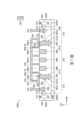
第1圖為本發明一些實施例之半導體裝置500A的剖面示意圖。在一些實施例中,半導體裝置500A包括蕭基二極體。如第1、2圖所示,在一些實施例中,半導體裝置500A包括半導體基板200、第一井區206、主體摻雜區208-1、208-2、隔離結構204以及電流分散摻雜區218-1、218-2。
FIG. 1 is a cross-sectional schematic diagram of a
在一些實施例中,半導體基板200包括元素半導體,例如矽(Si)、鍺(Ge)等;化合物半導體,例如氮化鎵(GaN)、
碳化矽(SiC)、砷化鎵(GaAs)、磷化鎵(GaP)、磷化銦(InP)、砷化銦(InAs)、銻化銦(InSb)等;合金半導體,例如矽鍺合金(SiGe)、磷砷鎵合金(GaAsP)、砷鋁銦合金(AlInAs)、砷鋁鎵合金(AlGaAs)、砷銦鎵合金(GaInAs)、磷銦鎵合金(GaInP)、磷砷銦鎵合金(GaInAsP)、或上述材料之組合。此外,半導體基板200也可包括絕緣層上覆半導體(semiconductor on insulator,SOI)。在一些實施例中,半導體基板200的導電類型可依設計需要為P型或N型。
In some embodiments, the
如第1圖所示,第一井區206和第二井區207設置於半導體基板200中。第二井區207圍繞且相鄰於第一井區206。在一些實施例中,半導體基板200的第一井區206包括陽極區330和陰極區332。並且,半導體裝置500A還包括設置於第二井區207上的接線摻雜區216。在一些實施例中,第一井區206具有第一導電類型。在一些實施例中,第二井區207和接線摻雜區216具有與第一導電類型相反的第二導電類型。舉例來說,第一井區206例如為N型高壓井區(HVNW)時,第二井區207例如為P型井區(例如P型高壓井區(HVPW)),而接線摻雜區216例如為P型接線摻雜區(P+)。在一些實施例中,半導體基板200藉由第二井區207及其上的接線摻雜區216電性連接最終半導體裝置500A的基極(Bulk)。然本發明並不以此為限,本領域技術人員可依照實際需求調整。在一些實施例中,接線摻雜區216的摻雜濃度大於第二井區207的摻雜濃度,第一井區
206和第二井區207的摻雜濃度大於半導體基板200的摻雜濃度。在一些實施例中,第一井區206的摻雜濃度約在1E15atoms/cm2至5E16atoms/cm2之間,第二井區207的摻雜濃度約在1E16atoms/cm2至5E17atoms/cm2之間,而接線摻雜區216的摻雜濃度約在5E18atoms/cm2至5E19atoms/cm2之間。
As shown in FIG. 1 , a
沿方向100(平行半導體基板200的方向)彼此間隔排列的多個主體摻雜區208-1、208-2、208-3、208-4、208-5設置於第一井區206上且接近半導體基板200的頂面201。在第1圖所示的剖面圖中,主體摻雜區208-1、208-2、208-3、208-4、208-5為指狀(finger-shaped)。並且,主體摻雜區208-1、208-2、208-3、208-4、208-5被第一井區206圍繞,主體摻雜區數量可依照實際需求調整。舉例來說,主體摻雜區208-1、208-2之間可具有比主體摻雜區208-1、208-2、208-3更多或更少的主體摻雜區,或不具有任何的主體摻雜區。在一些實施例中,主體摻雜區208-1、208-2、208-3、208-4、208-5具有第二導電類型。並且,主體摻雜區208-1、208-2、208-3、208-4、208-5的摻雜濃度大於第二井區207的摻雜濃度。在一些實施例中,主體摻雜區208-1、208-2、208-3、208-4、208-5的摻雜濃度約在2E17atoms/cm2至2E18atoms/cm2之間。於一實施例中,主體摻雜區208-1、208-2於上視圖中構成指狀或環狀結構,主體摻雜區208-3、208-5亦構成環狀結構。
A plurality of main doping regions 208-1, 208-2, 208-3, 208-4, 208-5 arranged in a direction 100 (a direction parallel to the semiconductor substrate 200) are disposed on the
在一些實施例中,在半導體裝置500A處於正向偏
壓時,導通電流主要流經陽極區330中的第一井區206。在一些實施例中,在半導體裝置500A處於逆向偏壓時,陽極區330中的主體摻雜區208-1、208-2、208-3、208-4、208-5之間的第一井區206中會產生空乏區,對關閉狀態漏電具有箝制作用(pinch)。
In some embodiments, when the
如第1圖所示,多個隔離結構204設置於第一井區206內、第一井區206的邊界206E上以及第一井區206外側的第二井區207中的半導體基板200上。在第1圖所示的剖面圖中,第一井區206內的隔離結構204圍繞部分主體摻雜區208-1、208-2、208-3、208-4、208-5,且分別與接近陽極區330邊緣的主體摻雜區208-1和主體摻雜區208-2部分重疊。在一些實施例中,第一井區206的底面206B和第二井區207的底面207B位於隔離結構204的底面下方。如第1圖所示,隔離結構204定義最終半導體裝置500A的陽極區330和陰極區332的形成位置。在一些實施例中,可依設計需要,於半導體基板200上設置任意數量的隔離結構204。在一些實施例中,隔離結構204為利用矽局部氧化(local oxidation of silicon,LOCOS)製程而形成的場氧化層(field oxide,FOX)、利用沉積製程形成的淺溝槽隔離(shallow trench isolation,STI)結構、或其他適合的隔離結構。在一些實施例中,使用熱氧化製程,包括乾氧化製程、濕氧化製程或其他適合的熱氧化製程來形成隔離結構204。
As shown in FIG. 1 , a plurality of
如第1圖所示,半導體裝置500A包括電流分散摻雜
區218-1、218-2。電流分散摻雜區218-1、218-2沿方向100彼此分離,且分別位於接近陽極區330邊緣的主體摻雜區208-1、208-2的正下方。電流分散摻雜區218-1、218-2沿方向110(垂直半導體基板200的方向)鄰接相應的主體摻雜區208-1、208-2的底面208B。並且,電流分散摻雜區218-1、218-2的相對側面218-1S、218-2S鄰接第一井區206。如第1圖所示的實施例中,電流分散摻雜區218-1、218-2位於第一井區206內且在方向110上與主體摻雜區208-1、208-2完全重疊。電流分散摻雜區218-1、218-2的相對側面218-1S、218-2S對齊主體摻雜區208-1、208-2的相對側面208-1S、208-2S。此外,電流分散摻雜區218-1、218-2的底面218B在第一井區206的底面206B上方。由於本實施例的電流分散摻雜區218-1、218-2相應接近陽極區330邊緣的主體摻雜區208-1、208-2設置,因此沿方向100位於主體摻雜區208-1、208-2之間的主體摻雜區208-3、208-4、208-5正下方不具有任何電流分散摻雜區。在一些實施例中,電流分散摻雜區218-1、218-2具有第一導電類型。並且,電流分散摻雜區218-1、218-2的摻雜濃度大於第一井區206的摻雜濃度。在一些實施例中,電流分散摻雜區218-1、218-2的摻雜濃度約在5E15atoms/cm2至1E17atoms/cm2之間。
As shown in FIG. 1 , the
如第1圖所示,半導體裝置500A還包括在半導體基板200中的第三井區210和設置於第三井區210上的接線摻雜區212。第三井區210和接線摻雜區212設置於第一井區206上。第三
井區210和接線摻雜區212接近於第一井區206的邊界206E,且分別與主體摻雜區208-1、208-2設置於隔離結構204的相對側。第三井區210和接線摻雜區212也分別與第二井區207設置於在第一井區206的邊界206E上的隔離結構204的相對側。如第1圖所示,第三井區210的底面210B位於第一井區206的底面206B和第二井區207的底面207B的上方。如第1圖所示,第三井區210及其正上方的接線摻雜區212圍繞主體摻雜區208-1、208-2、208-3、208-4、208-5。在一些實施例中,第三井區210和接線摻雜區212具有第一導電類型。舉例來說,第一井區206例如為N型高壓井區(HVNW)時,第三井區210例如為N型井區(例如N型低壓井區(NW)),而接線摻雜區212例如為N型接線摻雜區(N+)。然本發明並不以此為限,本領域技術人員可依照實際需求調整。在一些實施例中,接線摻雜區212的摻雜濃度大於第三井區210的摻雜濃度,第三井區210的摻雜濃度大於第一井區206的摻雜濃度。第一井區206藉由第三井區210及其上的接線摻雜區212電性連接最終半導體裝置500A的陰極區332。在一些實施例中,第三井區210的摻雜濃度約在5E16atoms/cm2至5E17atoms/cm2之間,接線摻雜區212的摻雜濃度約在5E18atoms/cm2至5E19atoms/cm2之間。
As shown in FIG. 1 , the
在一些實施例中,可利用多道離子植入製程,於半導體基板200中分別植入具有第一導電類型和第二導電類型的摻質以形成第一井區206、第二井區207、主體摻雜區208-1、208-2、208-3、208-4、208-5、第三井區210、接線摻雜區212、216和電流分散摻雜區218-1、218-2。在一些實施例中,第一導電類型的摻質例如為N型摻質,其可包括磷、砷、氮、銻、或上述之組合。在一些實施例中,第二導電類型的摻質例如P型摻質,其可包括硼、鎵、鋁、銦、三氟化硼離子(BF
3 +)、或上述之組合。
In some embodiments, a multi-pass ion implantation process may be used to implant dopants of the first conductivity type and the second conductivity type into the
如第1圖所示,半導體裝置500A更包括閘極結構228,設置於第一井區206內的半導體基板200上,並延伸覆蓋隔離結構204和相鄰的主體摻雜區208-1、208-2。在一些實施例中,閘極結構228包括設置於半導體基板200上的閘極介電層222、設置於閘極介電層222上方的閘極電極層224以及設置於閘極介電層222和閘極電極層224的側壁上的閘極間隔物226。閘極結構228可與半導體裝置的陽極區330電性連接,在半導體裝置500A處於逆向偏壓時具有電場分散作用,可提升半導體裝置500A的逆向偏壓下之電壓崩潰表現。As shown in FIG. 1 , the
在一些實施例中,閘極介電層222包括氧化矽(silicon oxide)、氮化矽(silicon nitride)、氮氧化矽(silicon oxynitride)、高介電常數材料、其他適合的介電材料、及/或上述之組合。上述之高介電常數材料例如為氧化鉿、氧化鉿矽、氮氧化鉿矽、氧化鉿鉭、氧化鉿鈦、氧化鉿鋯、氧化鋯、氧化鋁、氧化鉿-氧化鋁合金、及/或上述之組合或與其相似的材料。在一些實施例中,可使用氧化製程、沉積製程或其他合適之製程,於半導體基板200上形成閘極介電層222。In some embodiments, the
在一些實施例中,閘極電極層224包括多晶矽、非晶矽、金屬(例如鎢、鈦、鋁、銅、鉬、鎳、鉑、其他合適的金屬、或上述之組合)、金屬合金、金屬氮化物(例如氮化鎢、氮化鉬、氮化鈦、氮化鉭、其他合適的金屬氮化物、或上述之組合)、金屬氧化物(氧化釕、氧化銦錫、其他合適的金屬氧化物、或上述之組合)、其他合適的材料、或上述之組合。在一些實施例中,閘極電極層224可利用原位摻雜(in-situ doping)方式植入摻質。In some embodiments, the
在一些實施例中,閘極間隔物226包括氧化矽(silicon oxide)、氮化矽(silicon nitride)、氮氧化矽(silicon oxynitride)、低介電常數材料、其他適合的介電材料、及/或上述之組合。在一些實施例中,可使用氧化製程、沉積製程或其他合適之製程,以在閘極介電層222和閘極電極層224的側壁上形成閘極間隔物226。In some embodiments, the
如第1圖所示,半導體裝置500A更包括導電部件230,設置在半導體基板200上,且接觸(電性及/或物理接觸)第一井區206上的主體摻雜區208-1、208-2、208-3、208-4、208-5和主體摻雜區208-1、208-2、208-3、208-4、208-5之間的部分第一井區206。在一些實施例中,導電部件230電性連接閘極結構228。在一些實施例中,導電部件230可作為半導體裝置500A的陽極電極,其包括金屬(例如鎳(Ni)、鈷(Co)、鉑(Pt) 、鈦(Ti)、鎢(W)、鋁(Al)、上述之組合、或類似的材料)以與半導體基板200形成金屬矽化物。在一些實施例中,導電部件230也可包括摻雜多晶矽。在一些實施例中,可使用沉積製程(例如物理氣相沉積(PVD)、原子層沉積 (ALD)、濺鍍、或上述之組合)和後續的圖案化製程中形成導電部件230。As shown in FIG. 1 , the
第1圖所示,半導體裝置500A更包括導電部件232,設置在半導體基板200上,且接觸(電性及/或物理接觸) 第三井區210上的接線摻雜區212。在一些實施例中,導電部件232可作為半導體裝置500A的陰極電極,且可與導電部件230具有相同或類似的材料及製程。As shown in FIG. 1 , the
如第1圖所示,主體摻雜區208-1、208-2、208-3、208-4、208-5與主體摻雜區208-1、208-2、208-3、208-4、208-5之間的部分第一井區206作為例如為蕭基二極體的半導體裝置500A的陽極區330。並且,位於隔離結構204與主體摻雜區208-1、208-2相對側的部分第一井區206和其上的第三井區210作為例如為蕭基二極體的半導體裝置500A的陰極區332。換句話說,位於第一井區206的邊界206E與主體摻雜區208-1、208-2之間的部分第一井區206和其上的第三井區210作為例如為蕭基二極體的半導體裝置500A的陰極區332。在一些實施例中,半導體裝置500A的陽極區330包括電流分散摻雜區218-1、218-2。As shown in FIG. 1 , the main body doped regions 208-1, 208-2, 208-3, 208-4, 208-5 and a portion of the
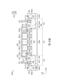
第2圖為本發明一些實施例之半導體裝置500B的剖面示意圖,圖中與第1圖相同或相似之元件符號表示相同或相似之元件。如第2圖所示,半導體裝置500B與半導體裝置500A的不同處為半導體裝置500B包括橫向尺寸(沿方向100的尺寸)較大的單一電流分散摻雜區220。如第2圖所示的實施例中,電流分散摻雜區220位於第一井區206內且與主體摻雜區208-1、208-2、208-3、208-4、208-5在方向110上部分重疊。電流分散摻雜區220在方向110上鄰接主體摻雜區208-1、208-2、208-3、208-4、208-5的底面208B(第1圖)。電流分散摻雜區220沿方向100延伸位於主體摻雜區208-1、208-2、208-3、208-4、208-5的正下方。並且,電流分散摻雜區220的相對側面220S鄰接第一井區206且分別對齊主體摻雜區208-1接近於隔離結構204的側面208-1S和主體摻雜區208-2隔離結構204的側面208-2S。此外,電流分散摻雜區220的底面220B在第一井區206的底面206B上方。在一些實施例中,半導體裝置500B的陽極區330還包括電流分散摻雜區220,且電流分散摻雜區218-1、218-2、220具有相同的導電類型和摻雜濃度。FIG. 2 is a cross-sectional schematic diagram of a
第3圖為本發明一些實施例之半導體裝置500C的剖面示意圖,圖中與第1、2圖相同或相似之元件符號表示相同或相似之元件。如第3圖所示,半導體裝置500C與半導體裝置500A的不同處為半導體裝置500C包括沿方向100彼此分離的電流分散摻雜區318-1、318-2。電流分散摻雜區318-1、318-2分別位於接近陽極區330邊緣的主體摻雜區208-1、208-2的正下方。電流分散摻雜區318-1、318-2沿方向110(垂直半導體基板200的方向)鄰接相應的主體摻雜區208-1、208-2的底面208B(第1圖)。並且,電流分散摻雜區318-1、318-2的相對側面318-1S、318-2S鄰接第一井區206及第一井區206下方的半導體基板200。如第3圖所示的實施例中,電流分散摻雜區318-1、318-2的底面318B在第一井區206的底面206B下方,以使第一井區206的底面206B位於的電流分散摻雜區318-1、318-2的頂面(同主體摻雜區208-1、208-2的底面208B)和底面318B之間。此外,電流分散摻雜區318-1、318-2在方向110上與主體摻雜區208-1、208-2完全重疊,且其相對側面318-1S、318-2S對齊主體摻雜區208-1、208-2的相對側面208-1S、208-2S。在一些實施例中,半導體裝置500C的陽極區330還包括電流分散摻雜區318-1、318-2,且電流分散摻雜區218-1、218-2、220、318-1、318-2具有相同的導電類型和摻雜濃度。電流分散摻雜區318-1、318-2的摻雜深度大於電流分散摻雜區218-1、218-2、220。於一實施例中,增加電流分散摻雜區318-1、318-2的摻雜深度可使半導體裝置500C的導通電阻降低以增加導通電流,相較於未設置電流分散摻雜區,元件導通電流(Ion)由0.23mA提升至0.41mA,Ion約可增加50%,崩潰電壓由93V提升至98V。FIG. 3 is a cross-sectional schematic diagram of a
第4圖為本發明一些實施例之半導體裝置500D的剖面示意圖,圖中與第1-3圖相同或相似之元件符號表示相同或相似之元件。如第4圖所示,半導體裝置500D與半導體裝置500C的不同處為半導體裝置500D包括橫向尺寸(沿方向100的尺寸)較大的單一電流分散摻雜區320。如第4圖所示的實施例中,電流分散摻雜區320與主體摻雜區208-1、208-2、208-3、208-4、208-5在方向110上部分重疊。電流分散摻雜區320的底面320B在第一井區206的底面206B下方,以使第一井區206的底面206B位於的電流分散摻雜區320的頂面(對齊主體摻雜區208-1、208-2、208-3、208-4、208-5的底面208B(第1圖))和底面320B之間。並且,電流分散摻雜區320在方向110上鄰接主體摻雜區208-1、208-2、208-3、208-4、208-5的底面208B。此外,電流分散摻雜區320沿方向100延伸位於主體摻雜區208-1、208-2、208-3、208-4、208-5的正下方。電流分散摻雜區320的相對側面320S鄰接第一井區206且分別對齊主體摻雜區208-1接近於隔離結構204的側面208-1S和主體摻雜區208-2隔離結構204的側面208-2S。在一些實施例中,半導體裝置500D的陽極區330還包括電流分散摻雜區320,且電流分散摻雜區218-1、218-2、220、318-1、318-2、320具有相同的導電類型和摻雜濃度。電流分散摻雜區320的摻雜深度大於電流分散摻雜區218-1、218-2、220。FIG. 4 is a cross-sectional schematic diagram of a
第5圖為本發明一些實施例之半導體裝置500E的剖面示意圖,圖中與第1-4圖相同或相似之元件符號表示相同或相似之元件。如第5圖所示,半導體裝置500E與半導體裝置500A的不同處為半導體裝置500E還包括沿方向100位於電流分散摻雜區218-1、218-2之間且彼此分離的電流分散摻雜區218-3、218-4、218-5,使電流分散摻雜區的數量與主體摻雜區的數量相同,且使多個彼此分離的電流分散摻雜區設置在每一個主體摻雜區的正下方。如第5圖所示的實施例中,電流分散摻雜區218-3、218-4、218-5分別位於主體摻雜區208-1、208-2之間的主體摻雜區208-3、208-4、208-5的正下方。電流分散摻雜區218-3、218-4、218-5與電流分散摻雜區218-1、218-2具有彼此對齊的頂面(相同於主體摻雜區208-1、208-2、208-3、208-4、208-5的底面208B(第1圖))和底面218B。並且,電流分散摻雜區218-3、218-4、218-5與相應的主體摻雜區208-3、208-4、208-5之間的位置關係可相同或類似於電流分散摻雜區218-1、218-2與相應的主體摻雜區208-1、208-2之間的位置關係。舉例來說,電流分散摻雜區218-3、218-4、218-5沿方向110(垂直半導體基板200的方向)鄰接相應的主體摻雜區208-3、208-4、208-5的底面208B。電流分散摻雜區218-3、218-4、218-5位於第一井區206內且在方向110上與主體摻雜區208-3、208-4、208-5完全重疊。並且,電流分散摻雜區218-3、218-4、218-5的相對側面218-3S、218-4S、218-5S對齊主體摻雜區208-3、208-4、208-5的相對側面208-3S、208-4S、208-5S。在一些實施例中,半導體裝置500E的陽極區330還包括電流分散摻雜區218-1、218-2、218-3、218-4、218-5,且電流分散摻雜區218-1、218-2、218-3、218-4、218-5、220、318-1、318-2、320具有相同的導電類型和摻雜濃度。FIG. 5 is a cross-sectional schematic diagram of a
第6圖為本發明一些實施例之半導體裝置500F的剖面示意圖,圖中與第1-5圖相同或相似之元件符號表示相同或相似之元件。如第6圖所示,半導體裝置500F與半導體裝置500B的不同處為半導體裝置500F包括從陽極區330橫向(沿方向100)延伸至陰極區332的單一電流分散摻雜區221。如第6圖所示的實施例中,電流分散摻雜區221延伸至第三井區210的正下方。並且,電流分散摻雜區221的相對側面221S鄰接第一井區206且對齊第三井區210接近於第一井區206的邊界206E的側面210S。此外,電流分散摻雜區221的底面221B在第一井區206的底面206B上方。在一些實施例中,半導體裝置500F的陽極區330和陰極區332還包括電流分散摻雜區221,且電流分散摻雜區218-1、218-2、218-3、218-4、218-5、220、221、318-1、318-2、320具有相同的導電類型和摻雜濃度。於一實施例中,電流分散摻雜區221的底面221B在第一井區206的底面206B下方,換句話說,電流分散摻雜區221摻雜深度較第一井區206深。FIG. 6 is a cross-sectional schematic diagram of a
第7圖為本發明一些實施例之半導體裝置500G的剖面示意圖,圖中與第1-6圖相同或相似之元件符號表示相同或相似之元件。如第7圖所示,半導體裝置500G與半導體裝置500C的不同處為半導體裝置500G還包括沿方向100位於電流分散摻雜區318-1、318-2之間且彼此分離的電流分散摻雜區318-3、318-4、318-5,使電流分散摻雜區的數量與主體摻雜區的數量相同,且使多個彼此分離的電流分散摻雜區設置在每一個主體摻雜區的正下方。如第7圖所示的實施例中,電流分散摻雜區318-3、318-4、318-5分別位於主體摻雜區208-1、208-2之間的主體摻雜區208-3、208-4、208-5的正下方。電流分散摻雜區318-3、318-4、318-5與電流分散摻雜區318-1、318-2具有彼此對齊的頂面(相同於主體摻雜區208-1、208-2、208-3、208-4、208-5的底面208B(第1圖))和底面318B。並且,電流分散摻雜區318-3、318-4、318-5與相應的主體摻雜區208-3、208-4、208-5之間的位置關係可相同或類似於電流分散摻雜區318-1、318-2與相應的主體摻雜區208-1、208-2之間的位置關係。舉例來說,電流分散摻雜區318-3、318-4、318-5沿方向110(垂直半導體基板200的方向)鄰接相應的主體摻雜區208-3、208-4、208-5的底面208B(第1圖)。電流分散摻雜區318-3、318-4、318-5在方向110上與主體摻雜區208-3、208-4、208-5完全重疊。並且,電流分散摻雜區318-3、318-4、318-5的相對側面318-3S、318-4S、318-5S對齊主體摻雜區208-3、208-4、208-5的相對側面208-3S、208-4S、208-5S。在一些實施例中,半導體裝置500G的陽極區330還包括電流分散摻雜區318-1、318-2、318-3、318-4、318-5,且電流分散摻雜區218-1、218-2、218-3、218-4、218-5、220、318-1、318-2、318-3、318-4、318-5、320具有相同的導電類型和摻雜濃度。FIG. 7 is a cross-sectional schematic diagram of a semiconductor device 500G according to some embodiments of the present invention, wherein the same or similar element symbols as those in FIGS. 1-6 represent the same or similar elements. As shown in FIG. 7 , the difference between the semiconductor device 500G and the
第8圖為本發明一些實施例之半導體裝置500I的剖面示意圖,圖中與第1-7圖相同或相似之元件符號表示相同或相似之元件。如第8圖所示,半導體裝置500I與半導體裝置500A的不同處為半導體裝置500I包括沿方向100彼此分離的電流分散摻雜區418-1、418-2。如第8圖所示的實施例中,電流分散摻雜區418-1、418-2從接近陽極區330邊緣的主體摻雜區208-1、208-2的正下方沿方向110延伸至主體摻雜區208-1、208-2之間且接近半導體基板200的頂面201,電流分散摻雜區418-1、418-2也延伸至主體摻雜區208-1、208-2與相鄰隔離結構204之間的部分第一井區206中。電流分散摻雜區418-1、418-2沿方向100分別鄰接主體摻雜區208-1、208-2的相對側面208-1S、208-2S。並且,電流分散摻雜區418-1、418-2分別包圍相應的主體摻雜區208-1、208-2的相對側面208-1S、208-2S和底面208B。因此,電流分散摻雜區418-1、418-2的相對側面418-1S、418-2S在相應的主體摻雜區208-1、208-2的相對側面208-1S、208-2S的外側,電流分散摻雜區418-1、418-2的底面418B在相應的主體摻雜區208-1、208-2的底面208B和第一井區206的底面206B之間。在一些實施例中,半導體裝置500I的陽極區330還包括電流分散摻雜區418-1、418-2,且電流分散摻雜區218-1、218-2、218-3、218-4、218-5、220、221、318-1、318-2、318-3、318-4、318-5、320具有相同的導電類型和摻雜濃度。電流分散摻雜區418-1、418-2可與電流分散摻雜區218-1、218-2、218-3、218-4、218-5、220、221具有相同的摻雜深度。FIG. 8 is a cross-sectional view of a semiconductor device 500I according to some embodiments of the present invention, wherein the same or similar element symbols as those in FIGS. 1-7 represent the same or similar elements. As shown in FIG. 8 , the difference between the semiconductor device 500I and the
第9圖為本發明一些實施例之半導體裝置500J的剖面示意圖,圖中與第1-8圖相同或相似之元件符號表示相同或相似之元件。如第9圖所示,半導體裝置500J與半導體裝置500I的不同處為半導體裝置500J還包括沿方向100位於電流分散摻雜區418-1、418-2之間且彼此分離的電流分散摻雜區418-3、418-4、418-5,使電流分散摻雜區的數量與主體摻雜區的數量相同,且使多個彼此分離的電流分散摻雜區從各相應的主體摻雜區的正下方沿方向110延伸至相鄰的主體摻雜區之間且接近半導體基板200的頂面201。如第9圖所示的實施例中,電流分散摻雜區418-3、418-4、418-5與電流分散摻雜區418-1、418-2具有彼此對齊的頂面(相同於半導體基板200的頂面201)和底面418B(第8圖)。並且,電流分散摻雜區418-3、418-4、418-5與相應的主體摻雜區208-3、208-4、208-5之間的位置關係可相同或類似於電流分散摻雜區418-1、418-2與相應的主體摻雜區208-1、208-2之間的位置關係。舉例來說,電流分散摻雜區418-3、418-4、418-5沿方向100分別鄰接主體摻雜區208-3、208-4、208-5的相對側面208-3S、208-4S、208-5S。並且,電流分散摻雜區418-3、418-4、418-5分別包圍相應的主體摻雜區208-3、208-4、208-52的相對側面208-3S、208-4S、208-5S和底面208B(第1圖)。因此,電流分散摻雜區418-3、418-4、418-5的相對側面418-3S、418-4S、418-5S在相應的主體摻雜區208-3、208-4、208-5的相對側面208-3S、208-4S、208-5S的外側,電流分散摻雜區418-3、418-4、418-5的底面418B(第8圖)在相應的主體摻雜區208-3、208-4、208-5的底面208B(第1圖)和第一井區206的底面206B之間。在一些實施例中,半導體裝置500J的陽極區330還包括電流分散摻雜區418-1、418-2、418-3、418-4、418-5,且電流分散摻雜區218-1、218-2、218-3、218-4、218-5、220、318-1、318-2、318-3、318-4、318-5、320、418-1、418-2、418-3、418-4、418-5具有相同的導電類型和摻雜濃度。FIG. 9 is a schematic cross-sectional view of a
第10圖為本發明一些實施例之半導體裝置500K的剖面示意圖,圖中與第1-9圖相同或相似之元件符號表示相同或相似之元件。如第10圖所示,半導體裝置500K與半導體裝置500F的不同處為半導體裝置500K包括從陽極區330橫向(沿方向100)延伸至陰極區332的單一電流分散摻雜區421。如第10圖所示的實施例中,電流分散摻雜區421從主體摻雜區208-1、208-2、208-3、208-4、208-5和第三井區210的正下方沿方向110延伸包圍主體摻雜區208-1、208-2、208-3、208-4、208-5和第三井區210且接近半導體基板200的頂面201。並且,電流分散摻雜區421的相對側面421S鄰接第一井區206。並且,電流分散摻雜區421沿方向100延伸至隔離結構204與主體摻雜區208-1、208-2相對側的部分第一井區206中。電流分散摻雜區421的相對側面421S沿方向100位於第三井區210接近第一井區206的邊界206E 的側面210S(第6圖)與第一井區206的邊界206E之間。此外,電流分散摻雜區421的底面421B在第一井區206的底面206B上方。在一些實施例中,半導體裝置500K的陽極區330和陰極區332還包括電流分散摻雜區421,且電流分散摻雜區218-1、218-2、218-3、218-4、218-5、220、221、318-1、318-2、318-3、318-4、318-5、320、418-1、418-2、418-3、418-4、418-5、421具有相同的導電類型和摻雜濃度。電流分散摻雜區421與電流分散摻雜區221可具有相同的摻雜深度。FIG. 10 is a cross-sectional schematic diagram of a
本發明實施例提供一種半導體裝置,例如蕭基二極體。半導體裝置在陽極區中具較高導通電流密度及較大電壓差的位置(接近陽極區邊緣之用以箝制關閉狀態漏電流的主體摻雜區的正下方位置)設置電流分散摻雜區。在一些實施例中,電流分散摻雜區具有與第一井區相同的導電類型且其摻雜濃度大於第一井區的摻雜濃度,電流分散摻雜區的深度可小於或大於第一井區的深度,以在不影響崩潰電壓和漏電的情形下可有效降低蕭基二極體的導通電阻。並且,由於上述電流分散摻雜區的設置可使電場分佈較為均勻,可進一步改善崩潰電壓。另外,電流分散摻雜區可與半導體裝置製程的深井區(deep well region)使用相同的光罩,可節省製程成本。在一些實施例中,可在各主體摻雜區周圍具較高導通電流密度及較大電壓差的位置(每一個主體摻雜區的正下方)設置相應的電流分散摻雜區。或者,可設置沿平行半導體基板方向延伸至每一個主體摻雜區的正下方的單一電流分散摻雜區。電流分散摻雜區也可從相應的主體摻雜區的正下方沿垂直半導體基板方向延伸接近半導體基板的頂面,或沿平行半導體基板方向從陽極區延伸至陰極區,以進一步降低陽極區的導通電阻以增加導通電流且改善崩潰電壓,提升半導體裝置的性能。The present invention provides a semiconductor device, such as a schottky diode. A current spreading doping region is provided in the semiconductor device at a position with a higher on-state current density and a larger voltage difference in the anode region (a position directly below a main doping region close to the edge of the anode region for clamping off-state leakage current). In some embodiments, the current spreading doping region has the same conductivity type as the first well region and its doping concentration is greater than the doping concentration of the first well region. The depth of the current spreading doping region can be less than or greater than the depth of the first well region, so as to effectively reduce the on-resistance of the schottky diode without affecting the breakdown voltage and leakage. Furthermore, since the provision of the above-mentioned current spreading doping region can make the electric field distribution more uniform, the breakdown voltage can be further improved. In addition, the current spreading doping region can use the same mask as the deep well region of the semiconductor device process, which can save process costs. In some embodiments, a corresponding current spreading doping region can be provided at a position with a higher conduction current density and a larger voltage difference around each main doping region (directly below each main doping region). Alternatively, a single current spreading doping region can be provided that extends in a direction parallel to the semiconductor substrate to directly below each main doping region. The current spreading doping region may also extend from directly below the corresponding main doping region in a direction perpendicular to the semiconductor substrate to approach the top surface of the semiconductor substrate, or extend from the anode region to the cathode region in a direction parallel to the semiconductor substrate, so as to further reduce the on-resistance of the anode region to increase the on-current and improve the breakdown voltage, thereby enhancing the performance of the semiconductor device.
雖然本發明以前述之實施例揭露如上,然其並非用以限定本發明。本發明所屬技術領域中具有通常知識者,在不脫離本發明之精神和範圍內,當可做些許之更動與潤飾。因此本發明之保護範圍當視後附之申請專利範圍所界定者為準。Although the present invention is disclosed as above by the aforementioned embodiments, they are not intended to limit the present invention. Those with ordinary knowledge in the technical field to which the present invention belongs may make some changes and modifications without departing from the spirit and scope of the present invention. Therefore, the scope of protection of the present invention shall be subject to the scope defined by the attached patent application.
100,110:方向 200:半導體基板 201:頂面 204:隔離結構 206:第一井區 206B,207B,208B,210B,218B,220B,221B,318B,320B,418B,421B:底面 206E:邊界 207:第二井區 208-1,208-2,208-3,208-4,208-5:主體摻雜區 208-1S,208-2S,208-3S,208-4S,208-5S,210S,218-1S,218-2S,218-3S,218-4S,218-5S,220S,221S,318-1S,318-2S,318-3S,318-4S,318-5S,320S, 418-1S,418-2S,418-3S,418-4S,418-5S,421S:側面 210:第三井區 212:接線摻雜區 216:接線摻雜區 218-1,218-2,218-3,218-4,218-5,220,221, 318-1,318-2,318-3,318-4,318-5,320, 418-1,418-2,418-3,418-4,418-5,421:電流分散摻雜區 222:閘極介電層 224:閘極電極層 226:閘極間隔物 228:閘極結構 230,232:導電部件 330:陽極區 332:陰極區500A,500B,500C,500D,500E,500F,500G,500I,500J,500K:半導體裝置 100,110: Direction 200: Semiconductor substrate 201: Top surface 204: Isolation structure 206: First well area 206B,207B,208B,210B,218B,220B,221B,318B,320B,418B,421B: Bottom surface 206E: Boundary 207: Second well area 208-1,208-2,208-3,208-4,208-5: Main body doping area 208-1S,208-2S,208-3S,208-4S,208-5S,210S,218-1S,218-2S,218-3S,218-4S,218-5S,220S,221S,318-1S,318-2S,318-3S,318-4S,318-5S,320S, 418-1S,418-2S,418-3S,418-4S,418-5S,421S: Side 210: Third well area 212: Wiring doping area 216: Wiring doping area 218-1,218-2,218-3,218-4,218-5,220,221, 318-1,318-2,318-3,318-4,318-5,320, 418-1,418-2,418-3,418-4,418-5,421: Current spreading doping region 222: Gate dielectric layer 224: Gate electrode layer 226: Gate spacer 228: Gate structure 230,232: Conductive component 330: Anode region 332: Cathode region 500A, 500B, 500C, 500D, 500E, 500F, 500G, 500I, 500J, 500K: Semiconductor device
當與所附圖式一起閱讀時,從以下詳細描述中可以更加理解本發明實施例的觀點。應注意的是,依據在業界的標準做法,各種特徵並未按照比例繪製且僅用以說明例示。事實上,可任意地放大或縮小元件的尺寸,以清楚地表現出本發明實施例的特徵。 第1-10圖為本發明一些實施例之半導體裝置的剖面示意圖。 When read in conjunction with the accompanying drawings, the following detailed description will provide a better understanding of the present invention. It should be noted that, in accordance with standard practice in the industry, various features are not drawn to scale and are provided for illustration purposes only. In fact, the size of the components may be arbitrarily enlarged or reduced to clearly illustrate the features of the present invention. Figures 1-10 are schematic cross-sectional views of semiconductor devices of some embodiments of the present invention.
100,110:方向
200:半導體基板
201:頂面
204:隔離結構
206:第一井區
206B,207B,208B,210B,218B:底面
206E:邊界
207:第二井區
208-1,208-2,208-3,208-4,208-5:主體摻雜區
208-1S,208-2S,218-1S,218-2S:側面
210:第三井區
212:接線摻雜區
216:接線摻雜區
218-1,218-2:電流分散摻雜區
222:閘極介電層
224:閘極電極層
226:閘極間隔物
228:閘極結構
230,232:導電部件
330:陽極區
332:陰極區
500A:半導體裝置
100,110: Direction
200: Semiconductor substrate
201: Top surface
204: Isolation structure
206: First well
Claims (15)
Priority Applications (1)
| Application Number | Priority Date | Filing Date | Title |
|---|---|---|---|
| TW112100186A TWI856473B (en) | 2023-01-04 | 2023-01-04 | Semiconductor device |
Applications Claiming Priority (1)
| Application Number | Priority Date | Filing Date | Title |
|---|---|---|---|
| TW112100186A TWI856473B (en) | 2023-01-04 | 2023-01-04 | Semiconductor device |
Publications (2)
| Publication Number | Publication Date |
|---|---|
| TW202429722A TW202429722A (en) | 2024-07-16 |
| TWI856473B true TWI856473B (en) | 2024-09-21 |
Family
ID=92928835
Family Applications (1)
| Application Number | Title | Priority Date | Filing Date |
|---|---|---|---|
| TW112100186A TWI856473B (en) | 2023-01-04 | 2023-01-04 | Semiconductor device |
Country Status (1)
| Country | Link |
|---|---|
| TW (1) | TWI856473B (en) |
Families Citing this family (1)
| Publication number | Priority date | Publication date | Assignee | Title |
|---|---|---|---|---|
| CN119132949A (en) * | 2024-09-03 | 2024-12-13 | 上海积塔半导体有限公司 | A Schottky device and a method for manufacturing the same |
Citations (5)
| Publication number | Priority date | Publication date | Assignee | Title |
|---|---|---|---|---|
| US20040227190A1 (en) * | 2003-05-14 | 2004-11-18 | Jun Cai | ESD protection for semiconductor products |
| US20050285188A1 (en) * | 2004-06-23 | 2005-12-29 | Khemka Vishnu K | LDMOS transistor |
| US20190140071A1 (en) * | 2017-11-04 | 2019-05-09 | Globalfoundries Singapore Pte. Ltd. | High voltage schottky diode and manufacturing method thereof |
| US20200381513A1 (en) * | 2011-09-20 | 2020-12-03 | Alpha And Omega Semiconductor Incorporated | Semiconductor chip integrating high and low voltage devices |
| US20220157982A1 (en) * | 2020-11-19 | 2022-05-19 | Richtek Technology Corporation | High voltage device of switching power supply circuit and manufacturing method thereof |
-
2023
- 2023-01-04 TW TW112100186A patent/TWI856473B/en active
Patent Citations (5)
| Publication number | Priority date | Publication date | Assignee | Title |
|---|---|---|---|---|
| US20040227190A1 (en) * | 2003-05-14 | 2004-11-18 | Jun Cai | ESD protection for semiconductor products |
| US20050285188A1 (en) * | 2004-06-23 | 2005-12-29 | Khemka Vishnu K | LDMOS transistor |
| US20200381513A1 (en) * | 2011-09-20 | 2020-12-03 | Alpha And Omega Semiconductor Incorporated | Semiconductor chip integrating high and low voltage devices |
| US20190140071A1 (en) * | 2017-11-04 | 2019-05-09 | Globalfoundries Singapore Pte. Ltd. | High voltage schottky diode and manufacturing method thereof |
| US20220157982A1 (en) * | 2020-11-19 | 2022-05-19 | Richtek Technology Corporation | High voltage device of switching power supply circuit and manufacturing method thereof |
Also Published As
| Publication number | Publication date |
|---|---|
| TW202429722A (en) | 2024-07-16 |
Similar Documents
| Publication | Publication Date | Title |
|---|---|---|
| KR102531554B1 (en) | Silicon Carbide Transistor And Fabrication Method Thereof | |
| US10770582B2 (en) | Semiconductor device | |
| US11489071B2 (en) | Semiconductor device | |
| US10629725B2 (en) | Semiconductor device having semiconductor regions with an interval therebetween in a gate pad region | |
| JP2014183259A (en) | Method for manufacturing semiconductor device and semiconductor device | |
| US10692969B1 (en) | Semiconductor structures | |
| KR101618979B1 (en) | Method for manufacturing a vertical semiconductor device and vertical semiconductor device | |
| JP5607947B2 (en) | Semiconductor device and manufacturing method thereof | |
| CN112201690A (en) | MOSFET transistor | |
| US11424357B2 (en) | Semiconductor device | |
| JP7680503B2 (en) | Vertical field effect transistor and method for forming same - Patents.com | |
| TWI856473B (en) | Semiconductor device | |
| US11411105B2 (en) | Silicon carbide semiconductor device | |
| TWI817691B (en) | Semiconductor device | |
| EP3905334B1 (en) | Power semiconductor device and manufacturing method therefor | |
| US12513924B2 (en) | Semiconductor device | |
| CN111446245A (en) | Semiconductor structure | |
| US12426330B2 (en) | Semiconductor device | |
| CN117727803A (en) | Semiconductor device with a semiconductor device having a plurality of semiconductor chips | |
| US20250176200A1 (en) | Semiconductor Structure and Manufacturing Method Thereof | |
| US20250393224A1 (en) | Semiconductor device | |
| US20260013155A1 (en) | Semiconductor device | |
| TWI891309B (en) | Semiconductor device | |
| CN120897485A (en) | A gallium oxide vertical trench MOSFET device and its fabrication method | |
| CN119451164A (en) | Semiconductor devices |