US9179556B2 - Preventing the formation of conductive anodic filaments in a printed circuit board - Google Patents
Preventing the formation of conductive anodic filaments in a printed circuit board Download PDFInfo
- Publication number
- US9179556B2 US9179556B2 US13/566,032 US201213566032A US9179556B2 US 9179556 B2 US9179556 B2 US 9179556B2 US 201213566032 A US201213566032 A US 201213566032A US 9179556 B2 US9179556 B2 US 9179556B2
- Authority
- US
- United States
- Prior art keywords
- tungsten nitride
- layer
- circuit board
- printed circuit
- copper
- Prior art date
- Legal status (The legal status is an assumption and is not a legal conclusion. Google has not performed a legal analysis and makes no representation as to the accuracy of the status listed.)
- Active, expires
Links
- 230000015572 biosynthetic process Effects 0.000 title description 6
- 229910052721 tungsten Inorganic materials 0.000 claims abstract description 60
- 239000010937 tungsten Substances 0.000 claims abstract description 60
- -1 tungsten nitride Chemical class 0.000 claims abstract description 56
- RYGMFSIKBFXOCR-UHFFFAOYSA-N Copper Chemical compound [Cu] RYGMFSIKBFXOCR-UHFFFAOYSA-N 0.000 claims abstract description 53
- 229910052802 copper Inorganic materials 0.000 claims abstract description 44
- 239000010949 copper Substances 0.000 claims abstract description 44
- 239000003365 glass fiber Substances 0.000 claims abstract description 30
- 238000000034 method Methods 0.000 claims abstract description 26
- 230000037361 pathway Effects 0.000 claims abstract description 15
- 238000000151 deposition Methods 0.000 claims description 11
- 239000003822 epoxy resin Substances 0.000 claims description 9
- 229920000647 polyepoxide Polymers 0.000 claims description 9
- 238000000231 atomic layer deposition Methods 0.000 claims description 7
- 238000005553 drilling Methods 0.000 claims description 6
- 238000009713 electroplating Methods 0.000 claims description 5
- QGZKDVFQNNGYKY-UHFFFAOYSA-N Ammonia Chemical compound N QGZKDVFQNNGYKY-UHFFFAOYSA-N 0.000 claims description 4
- 229910021529 ammonia Inorganic materials 0.000 claims description 2
- 230000000873 masking effect Effects 0.000 claims description 2
- WFKWXMTUELFFGS-UHFFFAOYSA-N tungsten Chemical compound [W] WFKWXMTUELFFGS-UHFFFAOYSA-N 0.000 claims description 2
- 230000004888 barrier function Effects 0.000 description 9
- 239000000463 material Substances 0.000 description 5
- 238000004090 dissolution Methods 0.000 description 3
- 230000008569 process Effects 0.000 description 3
- 239000004593 Epoxy Substances 0.000 description 2
- 239000002131 composite material Substances 0.000 description 2
- 230000008021 deposition Effects 0.000 description 2
- 229910052751 metal Inorganic materials 0.000 description 2
- 239000002184 metal Substances 0.000 description 2
- 230000004048 modification Effects 0.000 description 2
- 238000012986 modification Methods 0.000 description 2
- IVHJCRXBQPGLOV-UHFFFAOYSA-N azanylidynetungsten Chemical compound [W]#N IVHJCRXBQPGLOV-UHFFFAOYSA-N 0.000 description 1
- 239000011248 coating agent Substances 0.000 description 1
- 238000000576 coating method Methods 0.000 description 1
- 239000011187 composite epoxy material Substances 0.000 description 1
- 239000011889 copper foil Substances 0.000 description 1
- 239000003989 dielectric material Substances 0.000 description 1
- 239000004744 fabric Substances 0.000 description 1
- 239000000835 fiber Substances 0.000 description 1
- 239000011521 glass Substances 0.000 description 1
- 238000004519 manufacturing process Methods 0.000 description 1
- 230000007246 mechanism Effects 0.000 description 1
- 150000002739 metals Chemical class 0.000 description 1
- 230000003647 oxidation Effects 0.000 description 1
- 238000007254 oxidation reaction Methods 0.000 description 1
- 238000007747 plating Methods 0.000 description 1
- 229920001343 polytetrafluoroethylene Polymers 0.000 description 1
- 239000004810 polytetrafluoroethylene Substances 0.000 description 1
- 230000009467 reduction Effects 0.000 description 1
- 239000011347 resin Substances 0.000 description 1
- 229920005989 resin Polymers 0.000 description 1
- 238000009736 wetting Methods 0.000 description 1
Images

Classifications
-
- H—ELECTRICITY
- H05—ELECTRIC TECHNIQUES NOT OTHERWISE PROVIDED FOR
- H05K—PRINTED CIRCUITS; CASINGS OR CONSTRUCTIONAL DETAILS OF ELECTRIC APPARATUS; MANUFACTURE OF ASSEMBLAGES OF ELECTRICAL COMPONENTS
- H05K3/00—Apparatus or processes for manufacturing printed circuits
- H05K3/40—Forming printed elements for providing electric connections to or between printed circuits
- H05K3/42—Plated through-holes or plated via connections
- H05K3/421—Blind plated via connections
-
- H—ELECTRICITY
- H05—ELECTRIC TECHNIQUES NOT OTHERWISE PROVIDED FOR
- H05K—PRINTED CIRCUITS; CASINGS OR CONSTRUCTIONAL DETAILS OF ELECTRIC APPARATUS; MANUFACTURE OF ASSEMBLAGES OF ELECTRICAL COMPONENTS
- H05K2201/00—Indexing scheme relating to printed circuits covered by H05K1/00
- H05K2201/03—Conductive materials
- H05K2201/0302—Properties and characteristics in general
- H05K2201/0317—Thin film conductor layer; Thin film passive component
Definitions
- the present invention relates to printed circuit board structures that include internal copper structures.
- a typical printed circuit board includes insulating layers and conducting layers that are laminated together using an epoxy resin prepreg.
- the insulating layers are made with dielectric materials such as polytetrafluoroethylene, composite epoxy materials, or fiberglass-reinforced epoxy laminate.
- the conducting layers are made of conductive metals, such as a thin copper foil.
- a prepreg is a material having pre-impregnated composite fibers, such as a woven or unidirectional glass fiber mat that is already impregnated with an epoxy resin.
- the printed circuit board provides mechanical support for electronic components and provides electrically conductive pathways between those electronic components. These pathways may include traces formed on the surface of the printed circuit board or in any of the conducting layers. Some of the conducting layers may form other structures, such as a power plane or ground plane that supports the supply of electrical power to the electronic components on the board. Still further, the printed circuit board may include plated through holes that carry power or signals between the layers or surfaces of the board. A plated through hole (PTH) is formed by drilling a hole in the printed circuit board and then plating the walls of the hole with copper.
- PTH plated through hole
- the glass fibers that extend through the printed circuit board provide strength and dimensional stability to the board. For example, it may be important to prevent thermal expansion of a printed circuit board as its temperature increases so that the electrical connections between electronic components are not affected.
- One embodiment of the present invention provides a method of forming a via in a multilayer printed circuit board.
- the method comprises drilling a hole into the printed circuit board that is reinforced with glass fibers, wherein the hole extends between two conductive elements on different layers of the printed circuit board and cuts through a portion of the glass fibers.
- a tungsten nitride layer is then deposited on the walls of the hole, wherein the tungsten nitride layer has a thickness between 1.5 nanometers and 20 nanometers.
- the method further comprises depositing a copper layer over the tungsten nitride layer, wherein the copper and tungsten nitride form a conductive via that provides an electrically conductive pathway between the two conductive elements, and wherein the tungsten nitride layer isolates the copper layer from the glass fibers.
- Another embodiment of the invention provides an apparatus comprising a multilayer printed circuit board that is reinforced with glass fibers, and an electrically conductive via extending into the printed circuit board between two conductive elements on different layers of the printed circuit board and through a portion of the glass fibers.
- the via includes a tungsten nitride layer having a thickness between 1.5 nanometers and 20 nanometers and a copper layer over the tungsten nitride layer, such that the tungsten nitride layer isolates the copper layer from the glass fibers.
- FIG. 1 is a cross-sectional side view of a printed circuit board having a plated through hole in accordance with the present invention.
- FIG. 2 is a cross-sectional side view of a printed circuit board having a blind via in accordance with the present invention.
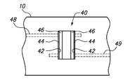
- FIG. 3 is a cross-sectional side view of a printed circuit board having a buried via in accordance with the present invention.
- One embodiment of the present invention provides a method of forming a via (“vertical interconnect access”) in a multilayer printed circuit board.
- the method comprises drilling a hole into a printed circuit board that is reinforced with glass fibers, wherein the hole extends between two conductive elements on different layers of the printed circuit board and cuts through a portion of the glass fibers.
- a tungsten nitride layer is then deposited on the walls of the hole, wherein the tungsten nitride layer has a thickness between 1.5 nanometers and 20 nanometers.
- the method further comprises depositing a copper layer over the tungsten nitride layer, wherein the copper and tungsten nitride form a conductive via that provides an electrically conductive pathway between the two conductive elements, and wherein the tungsten nitride layer isolates the copper layer from the glass fibers.
- Each end of a via typically terminates in a pad that makes electrical contact with conductive elements.
- a conductive element include an electronic component secured to printed circuit board, a conductive trace formed on the surface of the printed circuit board, and a conductive trace or plane within the printed circuit board.
- a typical printed circuit board will include at least one conductive power plane and at least one conductive ground plane.
- the printed circuit board may comprise an epoxy resin.
- the via extends between conductive layers of a printed circuit board.
- the via may be selected from a plated through hole, a blind via, and a buried via.
- a “plated through hole” extends through all of the layers of the printed circuit board from a top surface to a bottom surface.
- a “blind via” extends from one surface of the printed circuit board to an internal conductive component, such as a trace, power plane or ground plane.
- a “buried via” extends between two internal conductive components, without extending to either of the top or bottom surfaces of the printed circuit board.
- a tungsten nitride layer may be deposited on the walls of the hole using atomic layer deposition of tungsten nitride.
- a suitable vapor for use in the atomic layer deposition is bis(tert-butylimido)-bis-(dimethylamido)tungsten and ammonia.
- Such a process can produce a highly uniform, smooth, and conformal coating or layer of tungsten nitride (WN).
- the tungsten nitride layer serves as a barrier that prevents dissolution of the subsequently electroplated copper by isolating the copper from the glass cloth/resin interface, which may have undesirable pathways for conductive anodic filament (CAF) formation. By preventing copper dissolution, no conductive anodic filaments can be formed.
- CAF conductive anodic filament
- the tungsten nitride layer is electrically conductive and enables electrical contact to the copper traces or planes in the printed circuit board laminate.
- the tungsten nitride layer may be in direct contact with at least one of the two conductive elements.
- the method further comprises masking the printed circuit board prior to the atomic layer deposition.
- the mask serves to prevent deposition on unintended areas of the printed circuit board.
- the mask that was used during atomic layer deposition of the tungsten nitride is left in place during subsequent deposition of the copper layer. Then, the method may further comprise stripping the mask after depositing the copper layer.
- the step of depositing a copper layer over the tungsten nitride layer includes electroplating a copper layer over the tungsten nitride layer. During the copper electroplating, the tungsten nitride layer functions as a seed layer.
- Another embodiment of the invention provides an apparatus comprising a multilayer printed circuit board that is reinforced with glass fibers, and an electrically conductive via extending into the printed circuit board between two conductive elements on different layers of the printed circuit board and through a portion of the glass fibers.
- the via includes a tungsten nitride layer having a thickness between 1.5 nanometers and 20 nanometers and a copper layer over the tungsten nitride layer, such that the tungsten nitride layer isolates the copper layer from the glass fibers.
- the tungsten nitride layer may have a thickness between 1.5 nanometers and 20 nanometers
- the tungsten nitride layer preferably has a thickness between 1.5 nanometers and 10 nanometers.
- the multilayer printed circuit board may have any number of conductive layers alternating with dielectric layers, such as an epoxy resin composite. Consistent with the foregoing methods, the electrically conductive tungsten nitride layer may be in direct contact with at least one of the two conductive elements.
- the copper layer is disposed on the tungsten nitride layer such that the copper layer is isolated from the epoxy/glass fiber interface.
- the via may be selected from a plated through hole, a blind via, a buried via, or other types of vias now known or developed in the future.
- the tungsten nitride barrier of the present invention prevents the formation of conductive anodic filaments (CAF) that can form a conductive bridge between two copper structures.
- CAF conductive anodic filaments
- Conductive anodic filaments can form when there is an electrical bias between two copper structures and the printed circuit board contains a physical pathway between the two copper structures. These conditions often exist at a vertical interconnect access (via) that extends between conductive layers of a printed circuit board. If the epoxy resin and glass fiber separate or delaminate, perhaps due to poor wetting of the epoxy resin into the glass fiber weave during manufacture of the printed circuit board, physical pathways can form along the glass fibers. Upon drilling a hole into the printed circuit board, these glass fibers and pathways become exposed along the wall of the hole. When the hole is subsequently plated with copper, the copper comes into direct contact with the exposed ends of glass fibers and pathways.
- conductive anodic filaments are most common along a glass fiber bundle that extends between two plated through holes.
- FIG. 1 is a cross-sectional side view of a printed circuit board 10 having a plated through hole 20 in accordance with the present invention.
- Drilling through the printed circuit board 10 forms a cylindrical wall 22 that exposes the printed circuit board materials, such as epoxy resin and glass fibers (not shown). As discussed above, these glass fibers may partially separate from the epoxy resin layers and form open pathways through the printed circuit board 10 .
- the present invention includes a tungsten nitride barrier layer 24 applied over the cylindrical wall 22 .
- a copper layer 26 is then formed over the tungsten nitride barrier layer 24 , such as through an electroplating process.
- the copper material also forms circular pads 28 at the top and bottom surfaces of the printed circuit board 10 .
- An electrical component or conductive trace may be disposed in contact with one or both of the pads 28 in order to provide electronic communication therebetween.
- the tungsten nitride layer 24 is electrically conductive, such that the plated through hole 20 may be in electrical communication with any internal element 29 of the printed circuit board 10 that is made to come into contact with the via 20 .
- Examples of internal elements 29 include conductive traces, power planes, ground planes, or other discrete elements.
- FIG. 2 is a cross-sectional side view of a printed circuit board 10 having a blind via 30 in accordance with the present invention.
- the blind via 30 is formed with a hole that is drilled only partially through the thickness of the printed circuit board 10 .
- a tungsten nitride barrier layer 34 is applied over the cylindrical wall 32 and a copper layer 36 is then formed over the tungsten nitride barrier layer 34 .
- the tungsten nitride layer 34 forms a barrier to prevent the formation of conductive anodic filaments (CAF) in the printed circuit board 10 , but is electronically conductive to enable the plated blind via 30 to be in electrical communication with any internal element 39 of the printed circuit board 10 that is made to come into contact with the blind via 30 .
- An optional pad 38 may also be formed to facilitate contact with a component secured to the top surface of the printed circuit board 10 .
- FIG. 3 is a cross-sectional side view of a printed circuit board 10 having a buried via 40 in accordance with the present invention.
- the buried via 40 has a tungsten nitride layer 44 formed on the wall 42 of the buried via 40 and a copper layer 46 formed over the tungsten nitride barrier layer 44 .
- the tungsten nitride layer 44 forms a barrier to prevent the formation of conductive anodic filaments (CAF) in the printed circuit board 10 , but is electronically conductive to enable the plated blind via 30 to provide electrical communication between the internal elements 48 , 49 that come into contact with the buried via 40 .
- CAF conductive anodic filaments
Landscapes
- Engineering & Computer Science (AREA)
- Manufacturing & Machinery (AREA)
- Microelectronics & Electronic Packaging (AREA)
- Printing Elements For Providing Electric Connections Between Printed Circuits (AREA)
- Production Of Multi-Layered Print Wiring Board (AREA)
Abstract
Description
Claims (13)
Priority Applications (1)
| Application Number | Priority Date | Filing Date | Title |
|---|---|---|---|
| US13/566,032 US9179556B2 (en) | 2012-08-03 | 2012-08-03 | Preventing the formation of conductive anodic filaments in a printed circuit board |
Applications Claiming Priority (1)
| Application Number | Priority Date | Filing Date | Title |
|---|---|---|---|
| US13/566,032 US9179556B2 (en) | 2012-08-03 | 2012-08-03 | Preventing the formation of conductive anodic filaments in a printed circuit board |
Publications (2)
| Publication Number | Publication Date |
|---|---|
| US20140034375A1 US20140034375A1 (en) | 2014-02-06 |
| US9179556B2 true US9179556B2 (en) | 2015-11-03 |
Family
ID=50024372
Family Applications (1)
| Application Number | Title | Priority Date | Filing Date |
|---|---|---|---|
| US13/566,032 Active 2034-09-04 US9179556B2 (en) | 2012-08-03 | 2012-08-03 | Preventing the formation of conductive anodic filaments in a printed circuit board |
Country Status (1)
| Country | Link |
|---|---|
| US (1) | US9179556B2 (en) |
Cited By (1)
| Publication number | Priority date | Publication date | Assignee | Title |
|---|---|---|---|---|
| US10172243B2 (en) | 2016-11-14 | 2019-01-01 | International Business Machines Corporation | Printed circuit board and methods to enhance reliability |
Families Citing this family (1)
| Publication number | Priority date | Publication date | Assignee | Title |
|---|---|---|---|---|
| US11153976B2 (en) * | 2018-05-24 | 2021-10-19 | International Business Machines Corporation | Implementing IR reflective mask to minimize CTE mismatch between laminate and PTH copper |
Citations (15)
| Publication number | Priority date | Publication date | Assignee | Title |
|---|---|---|---|---|
| US4585502A (en) * | 1984-04-27 | 1986-04-29 | Hitachi Condenser Co., Ltd. | Process for producing printed circuit board |
| US4604314A (en) | 1984-01-27 | 1986-08-05 | Siemens Aktiengesellschaft | Printed circuit boards of laminated thermosetting sheets |
| US5052103A (en) * | 1988-11-04 | 1991-10-01 | Sharp Kabushiki Kaisha | Method of manufacturing printed wiring board having no copper migration |
| US6458696B1 (en) | 2001-04-11 | 2002-10-01 | Agere Systems Guardian Corp | Plated through hole interconnections |
| US6486063B2 (en) * | 2000-03-02 | 2002-11-26 | Tokyo Electron Limited | Semiconductor device manufacturing method for a copper connection |
| US6781064B1 (en) | 1996-08-20 | 2004-08-24 | International Business Machines Corporation | Printed circuit boards for electronic device packages having glass free non-conductive layers and method of forming same |
| US6939803B2 (en) | 2001-01-11 | 2005-09-06 | Advanced Micro Devices, Inc. | Method for forming conductor reservoir volume for integrated circuit interconnects |
| US20080164057A1 (en) | 2003-07-30 | 2008-07-10 | Hiroyuki Mori | Printed Wiring Board And Method Of Manufacturing Same |
| US20090233461A1 (en) * | 2008-03-17 | 2009-09-17 | Tourne Joseph A A M | Method of Manufacturing a Printed Circuit Board |
| US7615705B2 (en) | 2006-07-14 | 2009-11-10 | International Business Machines Corporation | Enhanced-reliability printed circuit board for tight-pitch components |
| US7627947B2 (en) | 2005-04-21 | 2009-12-08 | Endicott Interconnect Technologies, Inc. | Method for making a multilayered circuitized substrate |
| US7727809B2 (en) | 2006-05-31 | 2010-06-01 | Semiconductor Energy Laboratory Co., Ltd. | Attachment method, attachment apparatus, manufacturing method of semiconductor device, and manufacturing apparatus of semiconductor device |
| US20100193229A1 (en) | 2009-02-05 | 2010-08-05 | Xilinx, Inc. | Barrier layer to prevent conductive anodic filaments |
| US20110100697A1 (en) | 2009-10-29 | 2011-05-05 | International Business Machines Corporation | Interconnect structure having a via with a via gouging feature and dielectric liner sidewalls for beol integration |
| US8084863B2 (en) | 2005-03-23 | 2011-12-27 | Endicott Interconnect Technologies, Inc. | Circuitized substrate with continuous thermoplastic support film dielectric layers |
-
2012
- 2012-08-03 US US13/566,032 patent/US9179556B2/en active Active
Patent Citations (15)
| Publication number | Priority date | Publication date | Assignee | Title |
|---|---|---|---|---|
| US4604314A (en) | 1984-01-27 | 1986-08-05 | Siemens Aktiengesellschaft | Printed circuit boards of laminated thermosetting sheets |
| US4585502A (en) * | 1984-04-27 | 1986-04-29 | Hitachi Condenser Co., Ltd. | Process for producing printed circuit board |
| US5052103A (en) * | 1988-11-04 | 1991-10-01 | Sharp Kabushiki Kaisha | Method of manufacturing printed wiring board having no copper migration |
| US6781064B1 (en) | 1996-08-20 | 2004-08-24 | International Business Machines Corporation | Printed circuit boards for electronic device packages having glass free non-conductive layers and method of forming same |
| US6486063B2 (en) * | 2000-03-02 | 2002-11-26 | Tokyo Electron Limited | Semiconductor device manufacturing method for a copper connection |
| US6939803B2 (en) | 2001-01-11 | 2005-09-06 | Advanced Micro Devices, Inc. | Method for forming conductor reservoir volume for integrated circuit interconnects |
| US6458696B1 (en) | 2001-04-11 | 2002-10-01 | Agere Systems Guardian Corp | Plated through hole interconnections |
| US20080164057A1 (en) | 2003-07-30 | 2008-07-10 | Hiroyuki Mori | Printed Wiring Board And Method Of Manufacturing Same |
| US8084863B2 (en) | 2005-03-23 | 2011-12-27 | Endicott Interconnect Technologies, Inc. | Circuitized substrate with continuous thermoplastic support film dielectric layers |
| US7627947B2 (en) | 2005-04-21 | 2009-12-08 | Endicott Interconnect Technologies, Inc. | Method for making a multilayered circuitized substrate |
| US7727809B2 (en) | 2006-05-31 | 2010-06-01 | Semiconductor Energy Laboratory Co., Ltd. | Attachment method, attachment apparatus, manufacturing method of semiconductor device, and manufacturing apparatus of semiconductor device |
| US7615705B2 (en) | 2006-07-14 | 2009-11-10 | International Business Machines Corporation | Enhanced-reliability printed circuit board for tight-pitch components |
| US20090233461A1 (en) * | 2008-03-17 | 2009-09-17 | Tourne Joseph A A M | Method of Manufacturing a Printed Circuit Board |
| US20100193229A1 (en) | 2009-02-05 | 2010-08-05 | Xilinx, Inc. | Barrier layer to prevent conductive anodic filaments |
| US20110100697A1 (en) | 2009-10-29 | 2011-05-05 | International Business Machines Corporation | Interconnect structure having a via with a via gouging feature and dielectric liner sidewalls for beol integration |
Non-Patent Citations (1)
| Title |
|---|
| Becker et al., "Diffusion barrier properties of tungsten nitride films grown by atomic layer deposition from bis(tert-butylimido)bis (dimethylamido)tungsten and ammonia", http://apps.webofknowledge.com/OutboundService.do?action=go, Apr. 7, 2003, 1 Page. |
Cited By (1)
| Publication number | Priority date | Publication date | Assignee | Title |
|---|---|---|---|---|
| US10172243B2 (en) | 2016-11-14 | 2019-01-01 | International Business Machines Corporation | Printed circuit board and methods to enhance reliability |
Also Published As
| Publication number | Publication date |
|---|---|
| US20140034375A1 (en) | 2014-02-06 |
Similar Documents
| Publication | Publication Date | Title |
|---|---|---|
| US9888581B2 (en) | Method for manufacturing wiring board | |
| US10820420B2 (en) | Printed circuit boards with thick-wall vias | |
| JP4119205B2 (en) | Multilayer wiring board | |
| CN101802261B (en) | Multilayer printed wiring boards with holes requiring copper wrap plate | |
| US8541695B2 (en) | Wiring board and method for manufacturing the same | |
| US20120314389A1 (en) | Wiring board and method for manufacturing same | |
| KR20060105412A (en) | Double-sided wiring board manufacturing method, double-sided wiring board and its base | |
| US20090095509A1 (en) | Core substrate and method of producing the same | |
| US20090260868A1 (en) | Printed circuit board and method of manufacturing the same | |
| RU2015155524A (en) | SELECTIVE SEPARATION OF TRANSITION HOLES IN PRINTED CIRCUIT BOARDS | |
| US8186052B2 (en) | Method of producing substrate | |
| US8151456B2 (en) | Method of producing substrate | |
| US8035037B2 (en) | Core substrate and method of producing the same | |
| US20110284282A1 (en) | Wiring board and method for manufacturing the same | |
| US9179556B2 (en) | Preventing the formation of conductive anodic filaments in a printed circuit board | |
| JP2009252952A (en) | Copper charge plating method and printed circuit board manufactured by the method | |
| US9913382B2 (en) | Method for anchoring a conductive cap on a filled via in a printed circuit board and printed circuit board with an anchored conductive cap | |
| JP2009010266A (en) | Printed circuit board and method of manufacturing same | |
| CN109644551A (en) | Circuit board and its manufacturing method | |
| US20120012553A1 (en) | Method of forming fibrous laminate chip carrier structures | |
| TWI294263B (en) | Process for manufacturing a wiring substrate | |
| JP2009295635A (en) | Printed wiring board | |
| JP2017011215A (en) | Interposer and electronic apparatus including the same | |
| JP2004207338A (en) | Wiring board | |
| JP4328195B2 (en) | WIRING BOARD, MANUFACTURING METHOD THEREOF, AND ELECTRIC DEVICE |
Legal Events
| Date | Code | Title | Description |
|---|---|---|---|
| AS | Assignment |
Owner name: INTERNATIONAL BUSINESS MACHINES CORPORATION, NEW Y Free format text: ASSIGNMENT OF ASSIGNORS INTEREST;ASSIGNORS:KUCZYNSKI, JOSEPH;MILLER, MELISSA K.;WILLIAMS, HEIDI D.;AND OTHERS;REEL/FRAME:028727/0638 Effective date: 20120802 |
|
| FEPP | Fee payment procedure |
Free format text: PAYOR NUMBER ASSIGNED (ORIGINAL EVENT CODE: ASPN); ENTITY STATUS OF PATENT OWNER: LARGE ENTITY |
|
| AS | Assignment |
Owner name: LENOVO ENTERPRISE SOLUTIONS (SINGAPORE) PTE. LTD., SINGAPORE Free format text: ASSIGNMENT OF ASSIGNORS INTEREST;ASSIGNOR:INTERNATIONAL BUSINESS MACHINES CORPORATION;REEL/FRAME:034194/0111 Effective date: 20140926 Owner name: LENOVO ENTERPRISE SOLUTIONS (SINGAPORE) PTE. LTD., Free format text: ASSIGNMENT OF ASSIGNORS INTEREST;ASSIGNOR:INTERNATIONAL BUSINESS MACHINES CORPORATION;REEL/FRAME:034194/0111 Effective date: 20140926 |
|
| STCF | Information on status: patent grant |
Free format text: PATENTED CASE |
|
| AS | Assignment |
Owner name: LENOVO INTERNATIONAL LIMITED, HONG KONG Free format text: ASSIGNMENT OF ASSIGNORS INTEREST;ASSIGNOR:LENOVO ENTERPRISE SOLUTIONS (SINGAPORE) PTE. LTD.;REEL/FRAME:037696/0522 Effective date: 20160204 |
|
| MAFP | Maintenance fee payment |
Free format text: PAYMENT OF MAINTENANCE FEE, 4TH YEAR, LARGE ENTITY (ORIGINAL EVENT CODE: M1551); ENTITY STATUS OF PATENT OWNER: LARGE ENTITY Year of fee payment: 4 |
|
| AS | Assignment |
Owner name: LENOVO INTERNATIONAL LIMITED, HONG KONG Free format text: ASSIGNMENT OF ASSIGNORS INTEREST;ASSIGNOR:LENOVO ENTERPRISE SOLUTIONS (SINGAPORE) PTE LTD.;REEL/FRAME:050300/0947 Effective date: 20160101 |
|
| MAFP | Maintenance fee payment |
Free format text: PAYMENT OF MAINTENANCE FEE, 8TH YEAR, LARGE ENTITY (ORIGINAL EVENT CODE: M1552); ENTITY STATUS OF PATENT OWNER: LARGE ENTITY Year of fee payment: 8 |