US9166399B2 - Lithium battery protection circuitry - Google Patents
Lithium battery protection circuitry Download PDFInfo
- Publication number
- US9166399B2 US9166399B2 US13/807,635 US201113807635A US9166399B2 US 9166399 B2 US9166399 B2 US 9166399B2 US 201113807635 A US201113807635 A US 201113807635A US 9166399 B2 US9166399 B2 US 9166399B2
- Authority
- US
- United States
- Prior art keywords
- circuit
- transistor
- lithium battery
- coupled
- protection circuit
- Prior art date
- Legal status (The legal status is an assumption and is not a legal conclusion. Google has not performed a legal analysis and makes no representation as to the accuracy of the status listed.)
- Active, expires
Links
Images

Classifications
-
- H—ELECTRICITY
- H02—GENERATION; CONVERSION OR DISTRIBUTION OF ELECTRIC POWER
- H02H—EMERGENCY PROTECTIVE CIRCUIT ARRANGEMENTS
- H02H7/00—Emergency protective circuit arrangements specially adapted for specific types of electric machines or apparatus or for sectionalised protection of cable or line systems, and effecting automatic switching in the event of an undesired change from normal working conditions
- H02H7/18—Emergency protective circuit arrangements specially adapted for specific types of electric machines or apparatus or for sectionalised protection of cable or line systems, and effecting automatic switching in the event of an undesired change from normal working conditions for batteries; for accumulators
-
- H—ELECTRICITY
- H02—GENERATION; CONVERSION OR DISTRIBUTION OF ELECTRIC POWER
- H02J—CIRCUIT ARRANGEMENTS OR SYSTEMS FOR SUPPLYING OR DISTRIBUTING ELECTRIC POWER; SYSTEMS FOR STORING ELECTRIC ENERGY
- H02J7/00—Circuit arrangements for charging or depolarising batteries or for supplying loads from batteries
- H02J7/0029—Circuit arrangements for charging or depolarising batteries or for supplying loads from batteries with safety or protection devices or circuits
- H02J7/00302—Overcharge protection
-
- H—ELECTRICITY
- H02—GENERATION; CONVERSION OR DISTRIBUTION OF ELECTRIC POWER
- H02J—CIRCUIT ARRANGEMENTS OR SYSTEMS FOR SUPPLYING OR DISTRIBUTING ELECTRIC POWER; SYSTEMS FOR STORING ELECTRIC ENERGY
- H02J7/00—Circuit arrangements for charging or depolarising batteries or for supplying loads from batteries
- H02J7/0029—Circuit arrangements for charging or depolarising batteries or for supplying loads from batteries with safety or protection devices or circuits
- H02J7/00304—Overcurrent protection
-
- H—ELECTRICITY
- H02—GENERATION; CONVERSION OR DISTRIBUTION OF ELECTRIC POWER
- H02J—CIRCUIT ARRANGEMENTS OR SYSTEMS FOR SUPPLYING OR DISTRIBUTING ELECTRIC POWER; SYSTEMS FOR STORING ELECTRIC ENERGY
- H02J7/00—Circuit arrangements for charging or depolarising batteries or for supplying loads from batteries
- H02J7/0029—Circuit arrangements for charging or depolarising batteries or for supplying loads from batteries with safety or protection devices or circuits
- H02J7/00306—Overdischarge protection
-
- H—ELECTRICITY
- H02—GENERATION; CONVERSION OR DISTRIBUTION OF ELECTRIC POWER
- H02J—CIRCUIT ARRANGEMENTS OR SYSTEMS FOR SUPPLYING OR DISTRIBUTING ELECTRIC POWER; SYSTEMS FOR STORING ELECTRIC ENERGY
- H02J7/00—Circuit arrangements for charging or depolarising batteries or for supplying loads from batteries
- H02J7/0029—Circuit arrangements for charging or depolarising batteries or for supplying loads from batteries with safety or protection devices or circuits
- H02J7/0031—Circuit arrangements for charging or depolarising batteries or for supplying loads from batteries with safety or protection devices or circuits using battery or load disconnect circuits
-
- H02J2007/0039—
-
- Y—GENERAL TAGGING OF NEW TECHNOLOGICAL DEVELOPMENTS; GENERAL TAGGING OF CROSS-SECTIONAL TECHNOLOGIES SPANNING OVER SEVERAL SECTIONS OF THE IPC; TECHNICAL SUBJECTS COVERED BY FORMER USPC CROSS-REFERENCE ART COLLECTIONS [XRACs] AND DIGESTS
- Y02—TECHNOLOGIES OR APPLICATIONS FOR MITIGATION OR ADAPTATION AGAINST CLIMATE CHANGE
- Y02E—REDUCTION OF GREENHOUSE GAS [GHG] EMISSIONS, RELATED TO ENERGY GENERATION, TRANSMISSION OR DISTRIBUTION
- Y02E60/00—Enabling technologies; Technologies with a potential or indirect contribution to GHG emissions mitigation
- Y02E60/10—Energy storage using batteries
-
- Y02E60/12—
Definitions
- FIG. 1 shows a conventional lithium battery protection circuit.
- the protection circuit includes a control circuit 1 (integrated circuit or IC), high-voltage power transistors M 1 and M 2 , resistors R 1 and R 2 , and capacitor C 1 .
- the drain terminals of the power transistors M 1 and M 2 are connected together; the gate terminals of the power transistors M 1 and M 2 are connected to the control circuit 1 ; the source terminal of the power transistor M 1 is connected to the ground; and the source terminal of the power transistor M 2 is connected to one end of the resistor R 2 and also to the negative electrode “B ⁇ ” to external circuits.
- the other end of the resistor R 2 is connected to control circuit 1 .
- the control circuit 1 includes a bias and reference circuit, a multi-channel switch, an over-discharge protection circuit, and an over-charge protection circuit. Both the over-discharge protection circuit and the over-charge protection circuit are connected to the multi-channel switch.
- the over-discharge protection circuit and the over-charge protection circuit are also connected to logic circuit 2 via the delay circuit.
- the logic circuit 2 on the one hand, is connected to the gate terminals of power transistors M 1 and M 2 external to the control circuit 1 and, on the other hand, is connected to system sleep circuit 5 .
- the excessive-current protection circuit 3 and short-circuit protection circuit 4 are connected to resistor R 2 external to control circuit 1 , and also to the logic circuit 2 via the delay circuit.
- the logic circuit 2 turns off the power transistor M 2 , which further cuts off the charging circuit loop and stops charging tale lithium battery. After the power transistor M 2 is turned off, because no load current flows through the charging circuit loop, the charger's output voltage becomes higher than usual.
- the external circuit negative electrode “B ⁇ ” can have a negative high voltage (up to ⁇ 20V), which requires logic circuit 2 , excessive-current protection circuit 3 , short-circuit protection 4 , and power transistor M 2 to be able to withstand the negative high voltage. Meeting such requirement is necessary to ensure that the protection circuit can be used in high-voltage charging applications, and also improves reliability of the protection circuit under different application conditions.
- the logic circuit 2 During a discharging process, if the voltage of the lithium battery drops below an over-discharge protection voltage (usually 2V ⁇ 2.5V), and the low-voltage condition lasts longer than a specified delay time the logic circuit 2 turns off the power transistor M 1 , which stops the discharging. This condition may also show that the lithium battery has been exhausted. In order to better protect the lithium battery, logic circuit 2 also starts system sleep circuit 5 to put the entire control circuit 1 into a sleep state. Thus, the power consumed by the control circuit 1 itself can be reduced. Further, during the discharging process, if there is excessive-current or short-circuit condition, the logic circuit 2 also turns off the power transistor M 1 to stop the discharging to protect the lithium battery.
- an over-discharge protection voltage usually 2V ⁇ 2.5V
- the protection circuit as shown in FIG. 1 can achieve the goal of protecting the lithium battery during the charging/discharging processes, only the control circuit 1 is an integrated circuit, and other components in the protection circuit are external components. Thus, the degree of integration is relatively low and the manufacturing cost is relatively high.
- FIG. 2 shows another conventional lithium battery protection circuit.
- the previous external resistors R 1 and R 2 and the power transistor M 1 and M 2 are integrated into the control circuit 1 .
- Level shift circuit 6 and substrate switching circuit 7 are added to combine the power transistors M 1 and M 2 into one power transistor. Thus, the chip area and cost are reduced.
- the level shift circuit 6 is connected to the logic circuit 2 , the substrate switching circuit 7 , and the gate terminal of power transistor M 1 .
- the substrate switching circuit 7 is connected to the substrate of the power transistor M 1 and the level shift circuit 6 .
- the protection circuit as shown in FIG. 2 increases the degree of integration and lowers cost
- the excessive-current protection circuit 3 , short-circuit protection circuit 4 , level shift circuit 6 , and substrate switching circuit 7 generally use low-voltage MOS devices (a low-voltage MOS device may only be able withstand a relative low voltage between the gate-source and the source-drain).
- no other additional protective measures are used. Therefore, when protecting an overcharging condition, the protection circuit may be unable to withstand the high negative voltage from the external circuit negative electrode “B ⁇ ”.
- the protection circuit may have a low reliability and may be limited on its applications.
- the disclosed methods and systems are directed to solve one or more problems set forth above and other problems.
- the lithium battery protection circuit includes an over-charge protection circuit and a logic circuit coupled to over-charge protection circuit.
- the logic circuit has a first logic output and a second logic output.
- the lithium battery protection circuit also includes a level shift circuit coupled to the logic circuit through the first logic output and the second logic output, and the level shift circuit is configured to convert the first logic output and the second logic output to high voltage levels in an over-charge protection state.
- the lithium battery protection circuit includes a substrate switching circuit coupled to the level shift circuit and a power transistor coupled between a negative end of the lithium battery and an external circuit negative electrode.
- the lithium battery protection circuit includes a logic circuit having a first logic output and a second logic output, and a level shift circuit coupled to the logic circuit through the first logic output and the second logic output.
- the level shift circuit is configured to convert the first logic output and the second logic output to high voltage levels in an over-charge protection state.
- the lithium battery protection circuit also includes a substrate switching circuit coupled to the level shift circuit and a power transistor coupled between a negative end of the lithium battery and an external circuit negative electrode.
- the level shift circuit includes a first transistor coupled to the first logic output through a second transistor, and a first transistor group, including a third transistor connected in series, connected in parallel to a source and a drain of the first transistor.
- the level shift circuit also includes a fourth transistor coupled to the second logic output through a fifth transistor, and a second transistor group, including a sixth transistor connected in series, connected in parallel to a source and a drain of the fourth transistor.
- FIG. 1 shows a conventional protection circuit
- FIG. 2 shows another convention protection circuit
- FIG. 3 illustrates an exemplary lithium battery protection circuit consistent with the disclosed embodiments
- FIG. 5 illustrates another exemplary lithium battery protection circuit consistent with the disclosed embodiments.
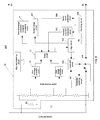
- FIG. 3 illustrates an exemplary lithium battery protection circuit 300 consistent with the disclosed embodiments.
- the positive end and the negative end of the lithium battery are coupled or connected to the external circuit positive electrode “B+” and negative electrode “B ⁇ ” respectively.
- Control circuit 16 (integrated circuit or IC) is coupled to the lithium battery through capacitor C 1 to form a lithium battery protection circuit.
- the lithium battery protection circuit includes control circuit 16 as an IC and capacitor C 1 .
- Control circuit 16 integrates a plurality of components. For example, a first resistor R 1 , a second resistor R 2 , the power transistor M 1 , a bias and reference circuit, a multi-channel switch, an over-discharge protection circuit, an over-charge protection circuit, a delay circuit, a logic circuit 302 , an excessive-current protection circuit 303 , a short-circuit protection circuit 304 , a system sleep circuit 305 , a level shift circuit 306 , a substrate switching circuit 307 , and a clamping circuit 308 . Certain component(s) may be omitted, and other component(s) may be included.
- the logic circuit 302 turns off the power transistor M 1 through the level shift circuit 306 .
- an over-charge protection voltage typically 4.2V ⁇ 4.3V
- the logic circuit 302 turns off the power transistor M 1 through the level shift circuit 306 .
- the charging circuit loop is broken and the charging is stopped.
- the logic circuit 302 turns off the power transistor M 1 through the level shift circuit 306 to stop discharging.
- the logic circuit 302 controls the system sleep circuit 305 to put the entire control circuit 16 into a sleep state, thereby greatly reducing the power consumption of the control circuit 16 .
- the logic circuit 302 also controls the level shift circuit 306 to turn off the power transistor M 1 to stop the discharging and to protect the lithium battery.
- the substrate switching circuit 307 switches the voltage level of the substrate of the power transistor M 1 to the lowest voltage level of 0V.
- the level shift circuit 306 and the substrate switching circuit 307 are configured to convert or switch the voltage levels of the gate terminal and the substrate of the power transistor M 1 .
- the clamping circuit 308 may limit the negative high voltage within a predetermined range ( ⁇ 2V ⁇ 3V).
- ⁇ 2V ⁇ 3V low-voltage MOS devices in the excessive-current protection circuit 303 and the short-circuit protection circuit 304 can be protected against the negative high voltage to avoid breakdown of these devices and/or circuits.
- the reliability of the lithium battery protection circuit can then be improved, and the range of applications of such protection circuit can be expanded.
- the clamping circuit 308 is not operational, and its output voltage level may be the same as the voltage level of the external circuit negative electrode “B ⁇ ”.
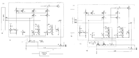
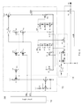
- FIG. 4 illustrates certain parts of an exemplary lithium battery protection circuit 400 in implementation details.
- the protection circuit 400 includes a logic circuit 15 (or logic circuit 302 ), a level shift circuit 13 (or level shift circuit 306 ), a substrate switching circuit 14 (or substrate switching circuit 307 ), a power transistor M 1 , and clamping circuit 11 . Certain components may be omitted and other components may be added. Further, the level shift circuit 13 may be coupled to the logic circuit 15 , the substrate switching circuit 14 may be coupled to the level shift circuit 13 and power transistor M 1 , and the clamping circuit 11 may be coupled between the external circuit negative electrode “B ⁇ ” and the substrate switching circuit 14 .
- the level shift circuit 13 may include a current source Ib, a PMOS current source formed by mirroring (including the first, second, third, and fifth PMOS transistors P 1 , P 2 , P 3 , and P 5 ), and an NMOS current source (including the first second, third, fourth, and eighth NMOS transistors N 1 , N 2 , N 3 , N 4 , and N 8 ).
- the level shift circuit 13 also includes the fourth and sixth PMOS transistors P 4 and P 6 for controlling voltage level shifting and flipping, a first group of NMOS transistors coupled to the fourth NMOS transistor N 4 and for limiting the source-drain voltage of the fourth NMOS transistor N 4 , a second group of NMOS transistors coupled to the eighth NMOS transistor N 8 and for limiting the source-drain voltage of the eighth transistor N 8 , and the seventh PMOS transistor P 7 and twelfth NMOS transistor N 12 for controlling the gate voltage of the power transistor M 1 .
- the first group of NMOS transistors may include a single NMOS transistor or two or more NMOS transistors connected in series in a diode form.
- the second group NMOS transistors may also include a single NMOS transistor or two or more NMOS transistors connected in series in the diode form.
- the first group may include three NMOS transistors connected in series as the fifth, sixth, and seventh NMOS transistors N 5 , N 6 , and N 7 ; and the second group may also include three NMOS transistors connected in series as the ninth, tenth, and eleventh NMOS transistors N 9 , N 10 , and N 11 .
- the current source Ib is coupled to the drain of the first NMOS transistor N 1 ; the second NMOS transistor N 2 and the first NMOS transistor N 1 are connected in the mirroring form; the gate and the drain of the first NMOS transistor N 1 are connected together; the source and the substrate of the first NMOS transistor N 1 are grounded; and the gate and the drain of the second NMOS transistor N 2 are also grounded.
- the mirroring form may refer to a form of connection of two or more MOS transistors where the gate terminals of the transistors are connected, the source terminals of the transistors are connected, the source and substrate of each MOS transistor are connected together, and the gate and the drain of at least one MOS transistor are connected together.
- a serial connection in the diode form may refer to a serial connection of two or more MOS transistors wherein the gate and drain of each MOS transistor are connected, the source and the drain of the adjacent two MOS transistors are connected, and the substrate of each MOS transistor is connected together and also to the source of the last MOS transistor.
- the fourth PMOS transistor P 4 is coupled in serial between the third PMOS transistor P 3 and the fourth NMOS transistor N 4 . That is, the source of the fourth PMOS transistor P 4 is connected to the drain of the third PMOS transistor P 3 ; the drain of the fourth PMOS transistor P 4 is connected to the drain of the fourth NMOS transistor N 4 (the node where the two drains are connected is marked as Sb); the substrate and the source of the fourth PMOS transistor P 4 are connected together; the gate of the fourth PMOS transistor P 4 is connected to the gate of the thirteenth NMOS transistor N 13 in the substrate switching circuit 14 , and the gate of the fourth PMOS transistor P 4 is connected to the output Sbi of the logic circuit 15 .
- the sixth PMOS transistor P 6 is coupled in serial between the fifth PMOS transistor P 5 and the eighth NMOS transistor N 8 . That is, the source of the sixth PMOS transistor P 6 is connected to the drain of the fifth PMOS transistor P 5 ; the drain of the sixth PMOS transistor P 6 is connected to the drain of the eighth NMOS transistor N 8 (the node where the two drains are connected is marked as Gt); the substrate and the source of the sixth PMOS transistor P 6 are connected together; and the gate of the sixth PMOS transistor P 6 is connected to the output Gti of the logic circuit 15 .
- the gate of the seventh PMOS transistor P 7 is coupled to the gate of the sixth PMOS transistor P 6 through the first inverter I 5 .
- the gate of the sixth PMOS transistor P 6 is connected to the input of the first inverter I 5
- the gate of the seventh PMOS transistor P 7 is connected to the output of the first inverter 5 .
- the source and the substrate of the seventh PMOS transistor P 7 are connected together, and the drain of the seventh PMOS transistor P 7 is connected to the gate of the power transistor M 1 .
- the gate of the twelfth NMOS transistor N 12 is connected to the gate of the eighth NMOS transistor N 8 , and the source of the twelfth NMOS transistor N 12 is connected to the source of the eighth NMOS transistor N 8 .
- the source and the substrate of the twelfth NMOS N 12 are connected together, and the drain of the twelfth NMOS transistor N 12 is connected to the gate of the power transistor M 1 , i.e., the drain of the twelfth NMOS transistor N 12 is connected to the drain of the seventh PMOS transistor P 7 (the node where the two drains are connected is marked as GtD).
- the substrate switching circuit 14 may include any appropriate components or circuits for switching the voltage level of the substrate of the power transistor M 1 .
- the substrate switching circuit 14 may include a thirteenth NMOS transistor N 13 , a fourteenth NMOS transistor N 14 , and a third resistor R 3 connected in serial between the source of the thirteenth NMOS transistor N 13 and the source of the fourteenth NMOS transistor N 14 .
- the drain of the thirteenth NMOS transistor N 13 is grounded and also connected to the source of the power transistor M 1 .
- the source of the thirteenth NMOS transistor N 13 is connected to an output of the clamping circuit 11
- the gate of the thirteenth NMOS transistor N 13 is connected to the level shift circuit 13 .
- the drain of the fourteenth NMOS transistor N 14 is connected to the external circuit negative electrode “B ⁇ ”; the gate of the fourteenth NMOS transistor N 14 is connected to the level shift circuit 13 ; and the source of the fourteenth NMOS transistor N 14 is connected to the substrate of the power transistor M 1 and also to the level shift circuit 13 .
- the source and the substrate of either the thirteenth NMOS transistor N 13 or the fourteenth NMOS transistor N 14 are connected together.
- the current source Ib may be generated by the bias and reference circuit, and the current in the first, second, third, fourth, and eighth NMOS transistors N 1 , N 2 , N 3 , N 4 , and N 8 and the first, second, third, and fifth PMOS transistor P 1 , P 2 , P 3 , and P 5 may be determined by the types and/or sizes of these transistors and the current source Ib.
- the first and second NMOS transistors N 1 and N 2 are ordinary low-voltage NMOS transistors; the third to the fourteenth NMOS transistor N 3 -N 14 are low-voltage substrate isolated NMOS transistors; and the first to the seventh PMOS transistor P 1 -P 7 are high source-drain voltage and low gate-source voltage PMOS transistors (i.e., being able to withstand high source-drain voltages but only low gate-source voltages).
- the voltage level between the node Sb and the substrate (“sub”) of the power transistor M 1 may be is limited to 3Vgs (3 times gate-source voltage of the NMOS transistor, about 2V ⁇ 3V).
- the fourth, fifth, sixth, and seventh NMOS transistors N 4 , N 5 , N 6 , and N 7 only need to withstand relatively low voltage levels.
- the eighth, ninth, tenth, and eleventh NMOS transistors N 8 , N 9 , N 10 , and N 11 also only need to withstand relatively low voltage levels.
- the third NMOS transistor N 3 is connected in the diode form (e.g., the gate and the drain being connected together), and the levels of the gate-source voltage and the source-drain voltage are also relatively low.
- the third NMOS transistor N 3 also only needs to withstand relatively low voltage levels.
- the clamping circuit 11 may limit the voltage level in a range of ⁇ 2V ⁇ 3V.
- the source voltage of the thirteenth NMOS transistor N 13 is also relatively low, and the thirteenth NMOS N 13 does not need to withstand relatively high voltage levels.
- the components described above in the level shift circuit 13 and substrate switching circuit 14 may carry out certain lithium protection functions.
- the highest voltage in the protection circuit may be the voltage of the lithium battery, which is generally low (e.g., 4.3V or lower).
- the logic circuit 15 controls the Sbi to output a high voltage level. At this time, the thirteenth NMOS transistor N 13 is turned on and the fourth PMOS transistor P 4 is turned off.
- the fourth PMOS transistor P 4 is turned off, no current flows through the fourth to the seventh NMOS transistors N 4 ⁇ N 7 , the voltage level of the node Sb is dropped down to the voltage level of the substrate of the power transistor M 1 (Vsub) by the fourth NMOS transistor N 4 , and the fourteenth NMOS transistor N 14 is turned off.
- the substrate of the power transistor M 1 is coupled to the ground through the third resistor R 3 and the thirteenth NMOS transistor N 13 and has a voltage level of 0V.
- the logic circuit 15 controls the Gti to output a high voltage level, which becomes a low voltage level through the first inverter I 5 , and the seventh PMOS transistor P 7 is turned on.
- the sixth PMOS transistor P 6 is turned off, the node Gt has a low voltage level, and the twelfth NMOS transistor N 12 is turned off.
- the node GtD has a high voltage level, the power transistor M 1 is turned on, and the lithium battery discharges normally.
- the logic circuit 15 controls the Sbi to output a low voltage level.
- the thirteenth NMOS transistors N 13 is turned off, the fourth PMOS transistor P 4 is turned on, the voltage level of node Sb is limited to 3Vgs (about 2V ⁇ 3V), the fourteenth NMOS transistor N 14 is turned on, and the voltage level of the substrate (Vsub) of power transistor M 1 is equal to voltage on the external circuit negative electrode “B ⁇ ”.
- the lithium battery has a low voltage and the power transistor M 1 is turned on, the entire circuit is still in a low-voltage state.
- the input signals Sbi and Gti are converted from low voltage levels (e.g., 0V) to high voltage levels (e.g., voltage 3Vgs+V B ⁇ , 3Vgs higher than the voltage level at the substrate of the power transistor M 1 ) to achieve voltage level conversion.
- the external circuit negative electrode “B ⁇ ” has a negative high voltage
- the nodes Sb and Gt also have a negative high voltage of 3Vgs+V B ⁇ .
- Such negative high voltage may be withstood by the third to the sixth PMOS transistor P 3 ⁇ P 6 , which have high source-drain voltages.
- the drain of the third NMOS transistor N 3 also has a negative high voltage, and such negative high voltage may be withstood by the second PMOS transistor P 2 .
- the nodes Sb and Gt have the negative high voltage, the voltage difference on the third to the eleventh NMOS transistors N 3 ⁇ N 11 does not exceed 3Vgs.
- the third to the eleventh NMOS transistors N 3 ⁇ N 11 still have low voltage levels and do not need to withstand high voltage level.
- the twelfth and fourteenth NMOS transistors N 12 and N 14 are turned on, the source-drain voltage of these transistors is close to 0V and the gate-source voltage of these transistors does not exceed 3Vgs.
- the twelfth and the fourteen NMOS transistors N 12 are N 14 only need to withstand low voltage levels.
- the clamming circuit 11 may limit the negative high voltage from the external circuit negative electrode “B ⁇ ” to a range of ⁇ 2V ⁇ 3V.
- the thirteenth NMOS transistor N 13 also only needs to withstand low voltage levels.
- the voltage difference across the third resistor R 3 may be large, and the third resistor R 3 may need to withstand high voltages.
- the third resistor R 3 may be high voltage polysilicon resistors.
- the external circuit negative electrode “B ⁇ ” has a negative high voltage
- the logic circuit 15 controls nodes Sbi and Gti to output a low voltage level (e.g., 0V).
- the low voltage level is converted into high voltage level of 3Vgs+V B ⁇ by level shift circuit 13 , and the twelfth and fourteenth NMOS transistors N 12 and N 14 are turned on.
- Such low voltage level also controls the substrate switching circuit 14 to convert between the low voltage level (e.g., 0V) and the voltage on the external circuit negative electrode “B ⁇ ”.
- the substrate switching circuit 14 also provides the converted voltage level to both the power transistor M 1 and the level shift circuit 13 .
- the negative high voltage on the external circuit negative electrode “B ⁇ ” is withstood by the second to the seventh PMOS transistor P 2 ⁇ P 7 with high source-drain voltages and the third resistor R 3 .
- the negative high voltage may appear on one end of the other low-voltage NMOS transistors, the voltage differences on those NMOS transistors are still small and, thus, high voltage NMOS transistors may be unnecessary.
- FIG. 5 illustrates another exemplary lithium battery protection circuit 500 consistent with the disclosed embodiments.
- the protection circuit 500 shown in FIG. 4 is similar to the protection circuit 400 in FIG. 4 .
- the substrate switching circuit 14 includes a second inverter I 8 , eighth and ninth PMOS transistors P 8 and P 9 with high source-drain voltages, and a fourteenth NMOS transistor N 14 .
- the input of the second inverter I 8 is connected to the gate of the fourth PMOS transistor P 4 in the level shift circuit 13 , and the output of the second inverter I 8 is connected to the gate terminals of the eighth and ninth PMOS transistors P 8 and P 9 .
- the source of the eighth PMOS transistor P 8 is connected to the source of the ninth PMOS transistor P 9 ; the source and the substrate of either the eighth PMOS transistor P 8 or the ninth PMOS transistor P 9 are connected together; and the drain of the eighth PMOS transistor P 8 is coupled to the ground and also coupled to the source of the power transistor M 1 .
- the drain of the ninth PMOS transistor P 9 is connected to the source of the fourteenth NMOS transistor N 14 and also connected to the substrate of the power transistor M 1 and the source of the fourth NMOS transistor N 4 in the level shift circuit 13 . Further, the gate of the fourteenth NMOS transistor N 14 is connected to the source of the fourth PMOS transistor P 4 in the level shift circuit 13 ; and the drain of the fourteenth NMOS transistor N 14 is connected to the external circuit negative electrode “B ⁇ ”.
- Substrate switching circuit 14 may operate during the lithium battery charging/discharging process. For example, during the lithium battery discharging process, the logic circuit 15 controls the Sbi to output a high voltage level, which becomes a low voltage level through the second inverter I 8 . The eighth and ninth PMOS transistors P 8 and P 9 are then turned on, and the fourteenth NMOS transistor N 14 is turned off.
- the voltage on the substrate of the power transistor M 1 (Vsub) needs to be shifted to the voltage level on the external circuit negative electrode “B ⁇ ”.
- the second inverter I 8 outputs a high voltage level
- the eighth and ninth PMOS transistors P 8 and P 9 are turned off
- the fourteenth NMOS transistor N 14 is turned on.
- the voltage of the substrate of the power transistor M 1 (Vsub) is also a high negative voltage.
- the high negative voltage is withstood by the eighth and ninth PMOS transistors P 8 and P 9 with high source-drain voltages, without the additional clamping circuit 11 and the third resistor R 3 as shown in FIG. 4 .
- the substrate switching circuit 14 can withstand high voltages without a clamping circuit.
- clamping circuit 11 is used in FIG. 4 and clamping circuit 308 is used in FIG. 3 , a single clamping circuit may be used to protect the excessive protection circuit, the short-circuit protection circuit, and the substrate switching circuit.
- FIG. 6 illustrates another exemplary lithium battery protection circuit 600 consistent with the disclosed embodiments.
- the lithium battery protection circuit 600 is similar to the lithium battery protection circuit 300 in FIG. 3 .
- lithium battery protection circuit 600 also includes an over-discharge-protection exception-processing circuit 9 that is integrated in the control circuit 16 .
- the over-discharge-protection exception-processing circuit 9 is connected to the over-discharge protection circuit 10 .
- the over-discharge-protection exception-processing circuit 9 is integrated into the control circuit 16 .
- the over-discharge-protection exception-processing circuit 9 is connected to the over-discharge protection circuit 10 .
- the over-discharge protection circuit 10 first analyzes the low-voltage situation of the lithium battery. If the over-discharge protection circuit 10 determines that the low voltage is caused by exceptions or abnormal discharging, the over-discharge-protection exception-processing circuit 9 is used to process the exceptions or abnormal discharging and to restore the lithium battery protection circuit 600 to the initial state or normal operational state from the sleep state.
Landscapes
- Engineering & Computer Science (AREA)
- Power Engineering (AREA)
- Charge And Discharge Circuits For Batteries Or The Like (AREA)
- Protection Of Static Devices (AREA)
- Secondary Cells (AREA)
Abstract
Description
Claims (20)
Applications Claiming Priority (4)
| Application Number | Priority Date | Filing Date | Title |
|---|---|---|---|
| CN201010581451.0 | 2010-12-09 | ||
| CN201010581451.0A CN102545162B (en) | 2010-12-09 | 2010-12-09 | Lithium battery protection circuit |
| CN201010581451 | 2010-12-09 | ||
| PCT/CN2011/083120 WO2012075896A1 (en) | 2010-12-09 | 2011-11-29 | Lithium battery protection circuitry |
Publications (2)
| Publication Number | Publication Date |
|---|---|
| US20130099755A1 US20130099755A1 (en) | 2013-04-25 |
| US9166399B2 true US9166399B2 (en) | 2015-10-20 |
Family
ID=46206611
Family Applications (1)
| Application Number | Title | Priority Date | Filing Date |
|---|---|---|---|
| US13/807,635 Active 2032-11-09 US9166399B2 (en) | 2010-12-09 | 2011-11-29 | Lithium battery protection circuitry |
Country Status (5)
| Country | Link |
|---|---|
| US (1) | US9166399B2 (en) |
| EP (1) | EP2630714B1 (en) |
| JP (1) | JP5718478B2 (en) |
| CN (1) | CN102545162B (en) |
| WO (1) | WO2012075896A1 (en) |
Cited By (3)
| Publication number | Priority date | Publication date | Assignee | Title |
|---|---|---|---|---|
| US20140167702A1 (en) * | 2012-12-17 | 2014-06-19 | Seiko Instruments Inc. | Charging and discharging control circuit and battery device |
| US10051718B2 (en) | 2016-08-03 | 2018-08-14 | Samsung Electronics Co., Ltd. | Mobile X-ray apparatus and method of operating the same |
| US10588209B2 (en) | 2016-08-03 | 2020-03-10 | Samsung Electronics Co., Ltd. | Mobile X-ray apparatus and method of operating the same |
Families Citing this family (20)
| Publication number | Priority date | Publication date | Assignee | Title |
|---|---|---|---|---|
| JP6202632B2 (en) * | 2012-09-18 | 2017-09-27 | Necエナジーデバイス株式会社 | Power storage system and battery protection method |
| CN103825252B (en) * | 2012-11-19 | 2017-03-15 | 比亚迪股份有限公司 | A kind of battery connects protective device and the protection system of broken string |
| CN103018655B (en) * | 2012-11-29 | 2015-03-11 | 无锡中星微电子有限公司 | Overcharge voltage detection circuit of battery protection circuit |
| DE102013219301A1 (en) * | 2013-09-25 | 2015-03-26 | Robert Bosch Gmbh | A method for effecting a sleep mode of a cell monitoring circuit of a lithium-ion secondary battery and lithium-ion secondary battery |
| TWI545863B (en) * | 2014-05-21 | 2016-08-11 | 廣達電腦股份有限公司 | Battery protection system and battery protection method |
| CN105337265B (en) * | 2014-06-30 | 2018-10-02 | 南京德朔实业有限公司 | Discharge protection circuit and control method thereof |
| CN104682355B (en) * | 2015-02-13 | 2018-03-30 | 深圳市富满电子集团股份有限公司 | A kind of lithium battery protection circuit |
| US9608615B2 (en) | 2015-06-12 | 2017-03-28 | Cypress Semiconductor Corporation | Negative high voltage hot switching circuit |
| CN105024435B (en) * | 2015-08-14 | 2017-11-03 | 重庆雅讯电源技术有限公司 | The power supply protection method and device of batteries |
| US10348079B2 (en) | 2015-08-27 | 2019-07-09 | Rohm Co., Ltd. | Overcurrent protective device, electronic apparatus, integrated circuit, and signal transmission circuit |
| US10686323B2 (en) * | 2016-08-30 | 2020-06-16 | Ablic Inc. | Charge/discharge control circuit and battery device including the same |
| CN108768361B (en) * | 2018-07-18 | 2024-07-05 | 富满微电子集团股份有限公司 | Substrate switching circuit for lithium battery protection |
| CN109104072B (en) * | 2018-09-14 | 2024-05-17 | 深圳南云微电子有限公司 | Compensation circuit for input voltage sampling |
| CN109831001B (en) * | 2019-01-29 | 2024-06-04 | 福建省福芯电子科技有限公司 | MOS tube driving circuit and lithium battery protection IC |
| CN110011378A (en) * | 2019-04-19 | 2019-07-12 | 深圳市山河动力电子有限公司 | A kind of lithium battery protection board overcurrent detection protection circuit |
| CN110098648B (en) * | 2019-04-24 | 2023-07-07 | 青岛海洋科技中心 | Energy management system for ocean observation detection buoy |
| EP3993205A4 (en) * | 2019-06-27 | 2022-08-31 | SANYO Electric Co., Ltd. | Battery pack, and abnormality monitoring method for same |
| CN113131446B (en) * | 2019-12-31 | 2024-08-30 | 圣邦微电子(北京)股份有限公司 | Battery protection circuit |
| CN112152288A (en) * | 2020-09-21 | 2020-12-29 | 深圳市创芯微微电子有限公司 | Battery protection circuit |
| CN112491117A (en) * | 2020-12-09 | 2021-03-12 | 上海芯跳科技有限公司 | Charging and discharging control circuit for lithium battery protection chip |
Citations (18)
| Publication number | Priority date | Publication date | Assignee | Title |
|---|---|---|---|---|
| US5530336A (en) * | 1992-09-17 | 1996-06-25 | Sony Corporation | Battery protection circuit |
| US6580250B1 (en) * | 2002-02-28 | 2003-06-17 | Dialog Semiconductor Gmbh | Monolithic battery protection circuit |
| US20030141847A1 (en) * | 2000-09-28 | 2003-07-31 | Akihiko Fujiwara | Charge/discharge protection apparatus having a charge-state overcurrent detector, and battery pack including the same |
| US6670939B2 (en) * | 2001-03-21 | 2003-12-30 | Myson-Century, Inc. | Single-ended high-voltage level shifter for a TFT-LCD gate driver |
| US6724173B2 (en) * | 2002-02-08 | 2004-04-20 | Valence Technology, Inc. | Circuits, apparatuses, electrochemical device charging methods, and lithium-mixed metal electrode cell charging methods |
| US6992463B2 (en) * | 2003-11-21 | 2006-01-31 | Texas Instruments Incorporated | Battery protection circuit |
| US6998668B2 (en) * | 2002-03-18 | 2006-02-14 | Renesas Technology Corp. | Semiconductor integrated circuit device including a level shifter |
| US7282890B2 (en) * | 2003-08-29 | 2007-10-16 | Yazaki Corporation | Voltage detector of battery assembly |
| US7504873B2 (en) * | 2005-04-07 | 2009-03-17 | Stmicroelectronics Sa | Voltage level shifting device |
| US7551497B2 (en) * | 2007-09-20 | 2009-06-23 | Mediatek Inc. | Memory circuits preventing false programming |
| US7583060B2 (en) * | 2004-09-07 | 2009-09-01 | Samsung Sdi Co., Ltd. | Protective circuit for a secondary battery pack and method of operating the same |
| US7629771B2 (en) * | 2006-02-09 | 2009-12-08 | O2Micro International, Ltd. | Protection device for non-common ground buses |
| US7694243B2 (en) * | 2007-12-27 | 2010-04-06 | International Business Machines Corporation | Avoiding device stressing |
| US7772805B2 (en) * | 2006-06-01 | 2010-08-10 | Ricoh Company, Ltd. | Charge/discharge protection circuit utilizing a charger connection recovery circuit that cycles a discharge control transistor on and off while a battery is over-discharged during charging |
| US8212529B2 (en) * | 2007-09-14 | 2012-07-03 | Ricoh Company, Ltd. | Charge/discharge protection circuit, battery pack including charge/discharge protection circuit, and electronic device thereof |
| US20120206105A1 (en) * | 2009-10-27 | 2012-08-16 | Mitsumi Electric Co., Ltd. | Charge-discharge control circuit, semiconductor integrated circuit, method of controlling charging and discharging, and charging and discharging control program |
| US20120306451A1 (en) * | 2010-02-26 | 2012-12-06 | Ricoh Company, Ltd. | Secondary cell protection circuit and battery |
| US8638121B2 (en) * | 2011-03-30 | 2014-01-28 | Takamasa Suzuki | Semiconductor device |
Family Cites Families (10)
| Publication number | Priority date | Publication date | Assignee | Title |
|---|---|---|---|---|
| JP3291530B2 (en) * | 1992-09-17 | 2002-06-10 | ソニー株式会社 | Battery protection circuit |
| JPH1084274A (en) * | 1996-09-09 | 1998-03-31 | Matsushita Electric Ind Co Ltd | Semiconductor logic circuit and circuit layout structure |
| US5936384A (en) * | 1997-06-09 | 1999-08-10 | Ricoh Company, Ltd. | Charge and discharge protection circuit and battery pack with high withstand voltage |
| EP1320168A1 (en) * | 2001-12-12 | 2003-06-18 | Dialog Semiconductor GmbH | Power switch for battery protection |
| JP4204446B2 (en) * | 2003-11-14 | 2009-01-07 | ソニー株式会社 | Battery pack, battery protection processing device, and activation control method for battery protection processing device |
| JP2007006048A (en) * | 2005-06-23 | 2007-01-11 | Matsushita Electric Ind Co Ltd | Semiconductor device for power |
| JP5194412B2 (en) * | 2006-09-19 | 2013-05-08 | 株式会社リコー | Back gate voltage generation circuit, four-terminal back gate switching FET, charge / discharge protection circuit using the FET, battery pack incorporating the charge / discharge protection circuit, and electronic device using the battery pack |
| CN101399440B (en) * | 2007-09-27 | 2011-03-30 | 比亚迪股份有限公司 | Protection circuit and method for multiple batteries |
| CN101404406B (en) * | 2008-07-15 | 2011-08-03 | 无锡华润上华科技有限公司 | Lithium battery protection circuit |
| JP2010142062A (en) * | 2008-12-15 | 2010-06-24 | Ricoh Co Ltd | Protection semiconductor device, and battery pack with the protection semiconductor device |
-
2010
- 2010-12-09 CN CN201010581451.0A patent/CN102545162B/en active Active
-
2011
- 2011-11-29 WO PCT/CN2011/083120 patent/WO2012075896A1/en active Application Filing
- 2011-11-29 JP JP2013542354A patent/JP5718478B2/en active Active
- 2011-11-29 US US13/807,635 patent/US9166399B2/en active Active
- 2011-11-29 EP EP11846783.6A patent/EP2630714B1/en active Active
Patent Citations (18)
| Publication number | Priority date | Publication date | Assignee | Title |
|---|---|---|---|---|
| US5530336A (en) * | 1992-09-17 | 1996-06-25 | Sony Corporation | Battery protection circuit |
| US20030141847A1 (en) * | 2000-09-28 | 2003-07-31 | Akihiko Fujiwara | Charge/discharge protection apparatus having a charge-state overcurrent detector, and battery pack including the same |
| US6670939B2 (en) * | 2001-03-21 | 2003-12-30 | Myson-Century, Inc. | Single-ended high-voltage level shifter for a TFT-LCD gate driver |
| US6724173B2 (en) * | 2002-02-08 | 2004-04-20 | Valence Technology, Inc. | Circuits, apparatuses, electrochemical device charging methods, and lithium-mixed metal electrode cell charging methods |
| US6580250B1 (en) * | 2002-02-28 | 2003-06-17 | Dialog Semiconductor Gmbh | Monolithic battery protection circuit |
| US6998668B2 (en) * | 2002-03-18 | 2006-02-14 | Renesas Technology Corp. | Semiconductor integrated circuit device including a level shifter |
| US7282890B2 (en) * | 2003-08-29 | 2007-10-16 | Yazaki Corporation | Voltage detector of battery assembly |
| US6992463B2 (en) * | 2003-11-21 | 2006-01-31 | Texas Instruments Incorporated | Battery protection circuit |
| US7583060B2 (en) * | 2004-09-07 | 2009-09-01 | Samsung Sdi Co., Ltd. | Protective circuit for a secondary battery pack and method of operating the same |
| US7504873B2 (en) * | 2005-04-07 | 2009-03-17 | Stmicroelectronics Sa | Voltage level shifting device |
| US7629771B2 (en) * | 2006-02-09 | 2009-12-08 | O2Micro International, Ltd. | Protection device for non-common ground buses |
| US7772805B2 (en) * | 2006-06-01 | 2010-08-10 | Ricoh Company, Ltd. | Charge/discharge protection circuit utilizing a charger connection recovery circuit that cycles a discharge control transistor on and off while a battery is over-discharged during charging |
| US8212529B2 (en) * | 2007-09-14 | 2012-07-03 | Ricoh Company, Ltd. | Charge/discharge protection circuit, battery pack including charge/discharge protection circuit, and electronic device thereof |
| US7551497B2 (en) * | 2007-09-20 | 2009-06-23 | Mediatek Inc. | Memory circuits preventing false programming |
| US7694243B2 (en) * | 2007-12-27 | 2010-04-06 | International Business Machines Corporation | Avoiding device stressing |
| US20120206105A1 (en) * | 2009-10-27 | 2012-08-16 | Mitsumi Electric Co., Ltd. | Charge-discharge control circuit, semiconductor integrated circuit, method of controlling charging and discharging, and charging and discharging control program |
| US20120306451A1 (en) * | 2010-02-26 | 2012-12-06 | Ricoh Company, Ltd. | Secondary cell protection circuit and battery |
| US8638121B2 (en) * | 2011-03-30 | 2014-01-28 | Takamasa Suzuki | Semiconductor device |
Cited By (3)
| Publication number | Priority date | Publication date | Assignee | Title |
|---|---|---|---|---|
| US20140167702A1 (en) * | 2012-12-17 | 2014-06-19 | Seiko Instruments Inc. | Charging and discharging control circuit and battery device |
| US10051718B2 (en) | 2016-08-03 | 2018-08-14 | Samsung Electronics Co., Ltd. | Mobile X-ray apparatus and method of operating the same |
| US10588209B2 (en) | 2016-08-03 | 2020-03-10 | Samsung Electronics Co., Ltd. | Mobile X-ray apparatus and method of operating the same |
Also Published As
| Publication number | Publication date |
|---|---|
| JP5718478B2 (en) | 2015-05-13 |
| EP2630714A4 (en) | 2013-12-04 |
| CN102545162B (en) | 2014-06-04 |
| EP2630714B1 (en) | 2016-04-06 |
| CN102545162A (en) | 2012-07-04 |
| US20130099755A1 (en) | 2013-04-25 |
| EP2630714A1 (en) | 2013-08-28 |
| WO2012075896A1 (en) | 2012-06-14 |
| JP2014500700A (en) | 2014-01-09 |
Similar Documents
| Publication | Publication Date | Title |
|---|---|---|
| US9166399B2 (en) | Lithium battery protection circuitry | |
| JP6614388B1 (en) | Secondary battery protection circuit, secondary battery protection device, battery pack, and control method of secondary battery protection circuit | |
| US6316915B1 (en) | Charge/discharge protection circuit and battery pack having the charge/discharge protection circuit | |
| JP5439800B2 (en) | Secondary battery protection integrated circuit device, secondary battery protection module using the same, and battery pack | |
| US6992463B2 (en) | Battery protection circuit | |
| US7719235B2 (en) | Charge/discharge protection circuit and power-supply unit | |
| US9099875B2 (en) | Reverse-connection protecting device and backup power supply including the same | |
| US9081069B2 (en) | Protection IC and method of monitoring a battery voltage | |
| US9142983B2 (en) | Battery protection IC and battery device | |
| US20120249087A1 (en) | Battery protection circuit, battery protection device, and battery pack | |
| KR102649721B1 (en) | Battery protection circuit and lithium battery system | |
| KR20050026360A (en) | Battery protection circuit | |
| US11462921B2 (en) | Secondary-battery protection circuit and battery pack | |
| CN112583079A (en) | Battery protection circuit and device | |
| JP7235987B2 (en) | Secondary battery protection circuit and battery pack | |
| KR20210101151A (en) | Charging/discharging control device and battery device |
Legal Events
| Date | Code | Title | Description |
|---|---|---|---|
| AS | Assignment |
Owner name: CSMC TECHNOLOGIES FAB1 CO., LTD., CHINA Free format text: ASSIGNMENT OF ASSIGNORS INTEREST;ASSIGNOR:LEI, SHUNHUI;REEL/FRAME:029550/0131 Effective date: 20121122 Owner name: CSMC TECHNOLOGIES FAB2 CO., LTD., CHINA Free format text: ASSIGNMENT OF ASSIGNORS INTEREST;ASSIGNOR:LEI, SHUNHUI;REEL/FRAME:029550/0131 Effective date: 20121122 |
|
| STCF | Information on status: patent grant |
Free format text: PATENTED CASE |
|
| MAFP | Maintenance fee payment |
Free format text: PAYMENT OF MAINTENANCE FEE, 4TH YEAR, LARGE ENTITY (ORIGINAL EVENT CODE: M1551); ENTITY STATUS OF PATENT OWNER: LARGE ENTITY Year of fee payment: 4 |
|
| AS | Assignment |
Owner name: CSMC TECHNOLOGIES FAB2 CO., LTD., CHINA Free format text: MERGER;ASSIGNOR:CSMC TECHNOLOGIES FAB1 CO., LTD.;REEL/FRAME:049039/0645 Effective date: 20170831 |
|
| MAFP | Maintenance fee payment |
Free format text: PAYMENT OF MAINTENANCE FEE, 8TH YEAR, LARGE ENTITY (ORIGINAL EVENT CODE: M1552); ENTITY STATUS OF PATENT OWNER: LARGE ENTITY Year of fee payment: 8 |