KR20210101151A - Charging/discharging control device and battery device - Google Patents
Charging/discharging control device and battery device Download PDFInfo
- Publication number
- KR20210101151A KR20210101151A KR1020210015373A KR20210015373A KR20210101151A KR 20210101151 A KR20210101151 A KR 20210101151A KR 1020210015373 A KR1020210015373 A KR 1020210015373A KR 20210015373 A KR20210015373 A KR 20210015373A KR 20210101151 A KR20210101151 A KR 20210101151A
- Authority
- KR
- South Korea
- Prior art keywords
- terminal
- discharge control
- charge
- nmos transistor
- voltage
- Prior art date
Links
Images


Classifications
-
- H—ELECTRICITY
- H02—GENERATION; CONVERSION OR DISTRIBUTION OF ELECTRIC POWER
- H02J—CIRCUIT ARRANGEMENTS OR SYSTEMS FOR SUPPLYING OR DISTRIBUTING ELECTRIC POWER; SYSTEMS FOR STORING ELECTRIC ENERGY
- H02J7/00—Circuit arrangements for charging or depolarising batteries or for supplying loads from batteries
- H02J7/007—Regulation of charging or discharging current or voltage
-
- H—ELECTRICITY
- H02—GENERATION; CONVERSION OR DISTRIBUTION OF ELECTRIC POWER
- H02J—CIRCUIT ARRANGEMENTS OR SYSTEMS FOR SUPPLYING OR DISTRIBUTING ELECTRIC POWER; SYSTEMS FOR STORING ELECTRIC ENERGY
- H02J7/00—Circuit arrangements for charging or depolarising batteries or for supplying loads from batteries
- H02J7/0029—Circuit arrangements for charging or depolarising batteries or for supplying loads from batteries with safety or protection devices or circuits
- H02J7/0034—Circuit arrangements for charging or depolarising batteries or for supplying loads from batteries with safety or protection devices or circuits using reverse polarity correcting or protecting circuits
-
- H—ELECTRICITY
- H02—GENERATION; CONVERSION OR DISTRIBUTION OF ELECTRIC POWER
- H02J—CIRCUIT ARRANGEMENTS OR SYSTEMS FOR SUPPLYING OR DISTRIBUTING ELECTRIC POWER; SYSTEMS FOR STORING ELECTRIC ENERGY
- H02J7/00—Circuit arrangements for charging or depolarising batteries or for supplying loads from batteries
- H02J7/0047—Circuit arrangements for charging or depolarising batteries or for supplying loads from batteries with monitoring or indicating devices or circuits
-
- H—ELECTRICITY
- H02—GENERATION; CONVERSION OR DISTRIBUTION OF ELECTRIC POWER
- H02J—CIRCUIT ARRANGEMENTS OR SYSTEMS FOR SUPPLYING OR DISTRIBUTING ELECTRIC POWER; SYSTEMS FOR STORING ELECTRIC ENERGY
- H02J7/00—Circuit arrangements for charging or depolarising batteries or for supplying loads from batteries
- H02J7/0069—Charging or discharging for charge maintenance, battery initiation or rejuvenation
-
- H—ELECTRICITY
- H02—GENERATION; CONVERSION OR DISTRIBUTION OF ELECTRIC POWER
- H02J—CIRCUIT ARRANGEMENTS OR SYSTEMS FOR SUPPLYING OR DISTRIBUTING ELECTRIC POWER; SYSTEMS FOR STORING ELECTRIC ENERGY
- H02J7/00—Circuit arrangements for charging or depolarising batteries or for supplying loads from batteries
- H02J7/007—Regulation of charging or discharging current or voltage
- H02J7/00712—Regulation of charging or discharging current or voltage the cycle being controlled or terminated in response to electric parameters
-
- H—ELECTRICITY
- H02—GENERATION; CONVERSION OR DISTRIBUTION OF ELECTRIC POWER
- H02M—APPARATUS FOR CONVERSION BETWEEN AC AND AC, BETWEEN AC AND DC, OR BETWEEN DC AND DC, AND FOR USE WITH MAINS OR SIMILAR POWER SUPPLY SYSTEMS; CONVERSION OF DC OR AC INPUT POWER INTO SURGE OUTPUT POWER; CONTROL OR REGULATION THEREOF
- H02M3/00—Conversion of dc power input into dc power output
- H02M3/02—Conversion of dc power input into dc power output without intermediate conversion into ac
- H02M3/04—Conversion of dc power input into dc power output without intermediate conversion into ac by static converters
- H02M3/10—Conversion of dc power input into dc power output without intermediate conversion into ac by static converters using discharge tubes with control electrode or semiconductor devices with control electrode
- H02M3/145—Conversion of dc power input into dc power output without intermediate conversion into ac by static converters using discharge tubes with control electrode or semiconductor devices with control electrode using devices of a triode or transistor type requiring continuous application of a control signal
- H02M3/155—Conversion of dc power input into dc power output without intermediate conversion into ac by static converters using discharge tubes with control electrode or semiconductor devices with control electrode using devices of a triode or transistor type requiring continuous application of a control signal using semiconductor devices only
- H02M3/156—Conversion of dc power input into dc power output without intermediate conversion into ac by static converters using discharge tubes with control electrode or semiconductor devices with control electrode using devices of a triode or transistor type requiring continuous application of a control signal using semiconductor devices only with automatic control of output voltage or current, e.g. switching regulators
-
- H—ELECTRICITY
- H02—GENERATION; CONVERSION OR DISTRIBUTION OF ELECTRIC POWER
- H02J—CIRCUIT ARRANGEMENTS OR SYSTEMS FOR SUPPLYING OR DISTRIBUTING ELECTRIC POWER; SYSTEMS FOR STORING ELECTRIC ENERGY
- H02J2207/00—Indexing scheme relating to details of circuit arrangements for charging or depolarising batteries or for supplying loads from batteries
- H02J2207/20—Charging or discharging characterised by the power electronics converter
-
- Y—GENERAL TAGGING OF NEW TECHNOLOGICAL DEVELOPMENTS; GENERAL TAGGING OF CROSS-SECTIONAL TECHNOLOGIES SPANNING OVER SEVERAL SECTIONS OF THE IPC; TECHNICAL SUBJECTS COVERED BY FORMER USPC CROSS-REFERENCE ART COLLECTIONS [XRACs] AND DIGESTS
- Y02—TECHNOLOGIES OR APPLICATIONS FOR MITIGATION OR ADAPTATION AGAINST CLIMATE CHANGE
- Y02E—REDUCTION OF GREENHOUSE GAS [GHG] EMISSIONS, RELATED TO ENERGY GENERATION, TRANSMISSION OR DISTRIBUTION
- Y02E60/00—Enabling technologies; Technologies with a potential or indirect contribution to GHG emissions mitigation
- Y02E60/10—Energy storage using batteries
Abstract
Description
본 발명은, 충방전 제어 회로 및 배터리 장치에 관한 것이다.The present invention relates to a charge/discharge control circuit and a battery device.
배터리 장치는, 이차 전지와, 이 이차 전지의 충방전을 제어하는 충방전 제어 회로를 포함하는 충방전 제어 장치를 구비하고 있다. 충방전 제어 장치는, 이차 전지의 과충전, 과방전, 방전 과전류, 및 충전 과전류를 검출하고, 검출 결과에 의거하여 이차 전지의 충방전을 제어한다. 배터리 장치는, 충방전 제어 장치가 이차 전지의 충방전을 제어함으로써, 이차 전지를 과충전, 과방전, 방전 과전류, 및 충전 과전류로부터 보호한다(예를 들면, 특허 문헌 1 참조).The battery device includes a secondary battery and a charging/discharging control device including a charging/discharging control circuit for controlling charging and discharging of the secondary battery. The charge/discharge control device detects overcharge, overdischarge, discharge overcurrent, and charge overcurrent of the secondary battery, and controls charge/discharge of the secondary battery based on the detection result. A battery device protects a secondary battery from overcharging, overdischarging, discharging overcurrent, and charging overcurrent by a charging/discharging control apparatus controlling charging/discharging of a secondary battery (for example, refer patent document 1).
그러나, 특허 문헌 1에 기재되는 배터리 장치는, 충전기의 극성을 반전시켜 외부 양극 단자 및 외부 음극 단자에 접속한, 이른바 역접속 상태를 상정하여 설계되어 있지 않다.However, the battery device described in Patent Document 1 is not designed assuming a so-called reverse connection state in which the polarity of the charger is reversed and connected to the external positive terminal and the external negative terminal.
구체적으로 설명하면, 외부 양극 단자 및 외부 음극 단자에 충전기를 역접속 한 상태에서는, 외부 양극 단자 및 외부 음극 단자에 충전기의 역전압이 인가된다. 따라서, 충전기의 전압과 이차 전지의 전압의 합에 상당하는 전압이, 이차 전지의 양극과 외부 양극 단자 사이에 인가된다. 이 결과, 이차 전지의 양극과 외부 양극 단자 사이에 설치되어 있는 충방전 제어 MOS 트랜지스터에 정격을 초과하는 과대한 전류가 흘러, 충방전 제어 회로 및 배터리 장치가 손상될 수 있다.Specifically, in a state in which the charger is connected to the external positive terminal and the external negative terminal in reverse, the reverse voltage of the charger is applied to the external positive terminal and the external negative terminal. Accordingly, a voltage corresponding to the sum of the voltage of the charger and the voltage of the secondary battery is applied between the positive electrode of the secondary battery and the external positive terminal. As a result, an excessive current exceeding the rating flows in the charge/discharge control MOS transistor provided between the positive electrode and the external positive terminal of the secondary battery, and the charge/discharge control circuit and the battery device may be damaged.
한편, 특허 문헌 1에 기재되는 배터리 장치에 있어서, 충전기의 역접속에 대한 보호 기능은, 당해 배터리 장치를 보호하는 보호 회로를 별도 설치함으로써 부가할 수 있다. 단, 별도의 보호 회로를 추가 설치하는 것은, 장치의 대형화를 초래해 버린다.On the other hand, in the battery device described in Patent Document 1, the protection function against the reverse connection of the charger can be added by separately providing a protection circuit for protecting the battery device. However, additional provision of a separate protection circuit will result in an increase in the size of the device.
본 발명은, 상술한 사정을 감안하여 이루어진 것이며, 보호 회로를 별도 설치하지 않고 역접속 상태로부터 배터리 장치를 보호 가능한 충방전 제어 회로 및 배터리 장치를 제공하는 것을 목적으로 한다.The present invention has been made in view of the above circumstances, and an object of the present invention is to provide a charge/discharge control circuit and a battery device capable of protecting a battery device from a reversed connection state without separately providing a protection circuit.
본 발명에 따른 충방전 제어 회로는, 이차 전지와, 부하 및 충전기의 양극 및 음극을 접속 가능한 외부 양극 단자 및 외부 음극 단자와, 상기 이차 전지의 충전을 제어하는 충전 제어 FET와, 상기 이차 전지의 방전을 제어하는 방전 제어 FET를 구비하는 배터리 장치의 충방전 제어 회로로서, 상기 이차 전지에 의해서 발생하는 제1 및 제2의 전원 전압 중, 제1의 전원 전압이 입력되는 제1의 전원 전압 입력 단자와, 상기 제1의 전원 전압보다 낮은 제2의 전원 전압이 입력되는 제2의 전원 전압 입력 단자와, 상기 충전 제어 FET의 게이트와 접속되는 충전 제어 단자와, 상기 방전 제어 FET의 게이트와 접속되는 방전 제어 단자와, 상기 외부 양극 단자에 인가되는 전압이 입력되는 전압 검출 단자와, 상기 방전 제어 단자와 상기 전압 검출 단자를 연락하는 NMOS 트랜지스터와, 상기 NMOS 트랜지스터의 드레인과 접속되는 컬렉터와, 상기 NMOS 트랜지스터의 소스와 접속되는 이미터와, 상기 NMOS 트랜지스터의 벌크 및 상기 제2의 전원 전압 입력 단자와 접속되는 베이스를 갖는 바이폴러 트랜지스터를 구비하는 것을 특징으로 한다.A charge/discharge control circuit according to the present invention comprises: a secondary battery; an external positive terminal and an external negative terminal connectable to the positive and negative electrodes of a load and a charger; a charge control FET for controlling charging of the secondary battery; A charge/discharge control circuit for a battery device having a discharge control FET for controlling discharge, wherein a first power voltage input from among first and second power voltages generated by the secondary battery is inputted a terminal, a second power supply voltage input terminal to which a second power supply voltage lower than the first power supply voltage is input, a charge control terminal connected to a gate of the charge control FET, and a gate of the discharge control FET a discharge control terminal to be used; a voltage detection terminal to which a voltage applied to the external anode terminal is input; an NMOS transistor connecting the discharge control terminal and the voltage detection terminal; and a collector connected to a drain of the NMOS transistor; and a bipolar transistor having an emitter connected to the source of the NMOS transistor, and a base connected to the bulk of the NMOS transistor and the second power supply voltage input terminal.
본 발명에 따른 배터리 장치는, 상술한 충방전 제어 회로와, 상기 이차 전지와, 상기 외부 음극 단자와, 상기 외부 양극 단자와, 상기 이차 전지의 양극과 상기 외부 양극 단자 사이에 접속되는 상기 충전 제어 FET 및 상기 방전 제어 FET를 구비한다.The battery device according to the present invention includes the above-described charge/discharge control circuit, the secondary battery, the external negative terminal, the external positive terminal, and the charge control connected between the positive electrode and the external positive terminal of the secondary battery. an FET and the discharge control FET.
본 발명에 의하면, 보호 회로를 별도 설치하지 않고 역접속 상태로부터 배터리 장치를 보호할 수 있다.ADVANTAGE OF THE INVENTION According to this invention, a battery device can be protected from the reverse connection state without providing a protection circuit separately.
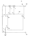
도 1은, 제1의 실시형태에 따른 배터리 장치의 구성예를 개략적으로 나타낸 회로도이다.
도 2는, 제1의 실시형태에 따른 충방전 제어 회로의 구성예를 개략적으로 나타낸 회로도이다.
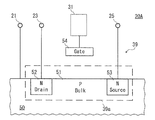
도 3은, 본 실시형태에 따른 충방전 제어 회로의 부분 단면을 개략적으로 나타낸 구조도이다.
도 4는, 본 실시형태에 따른 충방전 제어 회로에 적용되는 NMOS 트랜지스터와 당해 NMOS 트랜지스터에 기생하는 기생 바이폴러 트랜지스터의 관계를 개략적으로 나타낸 개략도이다.
도 5는, 본 실시형태에 따른 배터리 장치에 있어서, 충전기가 역접속된 상태를 나타낸 회로도이다.
도 6은, 제2의 실시형태에 따른 배터리 장치 및 충방전 제어 회로의 구성예를 개략적으로 나타낸 회로도이다.1 is a circuit diagram schematically showing a configuration example of a battery device according to a first embodiment.
Fig. 2 is a circuit diagram schematically showing a configuration example of a charge/discharge control circuit according to the first embodiment.
Fig. 3 is a structural diagram schematically showing a partial cross section of the charge/discharge control circuit according to the present embodiment.
4 is a schematic diagram schematically showing the relationship between an NMOS transistor applied to the charge/discharge control circuit according to the present embodiment and a parasitic bipolar transistor parasitic in the NMOS transistor.
5 is a circuit diagram showing a state in which the charger is connected in reverse in the battery device according to the present embodiment.
6 is a circuit diagram schematically showing a configuration example of a battery device and a charge/discharge control circuit according to the second embodiment.
이하, 본 발명의 실시형태에 따른 충방전 제어 회로 및 배터리 장치를, 도면을 참조하여 설명한다.DETAILED DESCRIPTION OF THE PREFERRED EMBODIMENTS Hereinafter, a charge/discharge control circuit and a battery device according to an embodiment of the present invention will be described with reference to the drawings.
[제1의 실시형태][First embodiment]
도 1은, 제1의 실시형태에 따른 배터리 장치의 구성예를 나타내는 회로도이다. 배터리 장치(1A)는 제1의 실시형태에 따른 배터리 장치의 일례이며, 충방전 제어 회로(20A)는 제1의 실시형태에 따른 충방전 제어 회로의 일례이다.1 is a circuit diagram showing a configuration example of a battery device according to a first embodiment. The
배터리 장치(1A)는, 충방전 제어 회로(20A)와, 이차 전지(SC)와, N형의 MOS 트랜지스터(이하, 「NMOS 트랜지스터」라고 한다.)(3, 4)와, 외부 양극 단자(EB+)와, 외부 음극 단자(EB-)를 구비하고 있다.The
충방전 제어 회로(20A)는, 제1의 전원 전압 입력 단자로서의 VDD 단자(21)와, 제2의 전원 전압 입력 단자로서의 VSS 단자(22)와, 충전 제어 단자(23)와, 방전 제어 단자(24)와, 전압 검출 단자(25)를 구비하고 있다.The charge/
VDD 단자(21)는 제1의 전원 전압으로서의 전압(VDD)이 입력되는 단자이다. VDD 단자(21)는 이차 전지(SC)의 양극 및 NMOS 트랜지스터(3)의 소스에 접속되어 있다. 이차 전지(SC)의 양극, NMOS 트랜지스터(3)의 소스 및 VDD 단자(21)의 접속점은, 노드(N1)를 형성하고 있다.The
VSS 단자(22)는 제2의 전원 전압으로서의 전압(VSS)이 입력되는 단자이다. VSS 단자(22)는 저항(5)을 개재하여 접지 단자(GND)에 접속되어 있다. 저항(5)의 일단은 외부 음극 단자(EB-) 및 이차 전지(SC)의 음극과 접속되어 있다. 저항(5)의 일단, 외부 음극 단자(EB-) 및 이차 전지(SC)의 음극의 접속점은, 노드(N2)를 형성하고 있다. 저항(5)은, 후술하는 바와 같이, 역접속 상태에 발생하는 VSS 단자(22)로부터 전압 검출 단자(25)로 기생 바이폴러 트랜지스터(39a)(후술하는 도 2)의 베이스·이미터 간 다이오드를 통해 흐르는 전류를 제한하는 기능을 갖는다.The
충전 제어 FET(전계 효과 트랜지스터)로서의 NMOS 트랜지스터(3)는, 충전 제어 단자(23)와 접속되는 게이트와, 이차 전지(SC)의 양극 및 VDD 단자(21)와 접속되는 소스와, 드레인을 갖고, 이차 전지(SC)의 충전을 제어한다.The
방전 제어 FET로서의 NMOS 트랜지스터(4)는, 방전 제어 단자(24)와 접속되는 게이트와, NMOS 트랜지스터(3)의 드레인과 접속되는 드레인과, 전압 검출 단자(25)와 단락되는 소스를 갖고, 이차 전지(SC)의 방전을 제어한다. NMOS 트랜지스터(4)의 소스와 전압 검출 단자(25)의 접속점은 노드(N3)를 형성하고 있다.The
외부 양극 단자(EB+)는, 부하 및 충전기의 양극과 접속 가능하게 구성되어 있다. 외부 양극 단자(EB+)는, 노드(N3)에 접속되어 있다. 외부 음극 단자(EB-)는, 부하 및 충전기의 음극과 접속 가능하게 구성되어 있다. 외부 음극 단자(EB-)는, 노드(N2)에 접속되어 있다.The external positive terminal EB+ is configured to be connectable to the positive electrode of the load and the charger. The external positive terminal EB+ is connected to the node N3. The external negative terminal EB- is configured to be connectable to the negative electrode of the load and the charger. The external negative terminal EB- is connected to the node N2.
도 2는, 충방전 제어 회로(20A)의 보다 구체적인 구성을 나타내는 회로도이다. 2 is a circuit diagram showing a more specific configuration of the charge/
충방전 제어 회로(20A)는, 상술한 VDD 단자(21), VSS 단자(22), 충전 제어 단자(23), 방전 제어 단자(24) 및 전압 검출 단자(25) 외에, 제어 회로(31)와, 승압 회로(32)와, P형의 MOS 트랜지스터(이하, 「PMOS 트랜지스터」라고 한다.)(33, 34)와, 레벨 시프터(37, 38)와, NMOS 트랜지스터(39)와, 기생 바이폴러 트랜지스터(39a)를 구비하고 있다.The charge/
제어 회로(31)는, VDD 단자(21) 및 VSS 단자(22)의 사이에 접속되어 있다. 또, 제어 회로(31)는, 승압 회로(32), 레벨 시프터(37, 38)를 개재하여 PMOS 트랜지스터(33, 34)의 게이트, 및 NMOS 트랜지스터(39)의 게이트에 접속되어 있다. 제어 회로(31)는, 승압 회로(32)의 출력 전압의 온 및 오프, PMOS 트랜지스터(33, 34)의 온 및 오프 및 NMOS 트랜지스터(39)의 온 및 오프를 제어한다.The
승압 회로(32)는, VDD 단자(21) 및 VSS 단자(22) 사이에 접속되어 있고, 전압(VDD)보다 높은 전압을 발생 가능하게 구성되어 있다. 또, 충방전 제어 회로(20A)에 있어서, 승압 회로(32)는, 발생시킨 전압을 출력하는 복수의 출력단으로서, 적어도 충전 제어 단자(23)와 접속되는 출력단과, 방전 제어 단자(24)와 접속되는 출력단을 갖고 있다. 승압 회로(32)는, 제어 회로(31)와 접속되는 제어 단자를 갖고 있다. 승압 회로(32)는, 제어 단자로부터 입력되는 제어 신호에 의거하여 자기의 출력단마다 출력 전압의 온 및 오프가 제어된다.The
PMOS 트랜지스터(33, 34)는, 둘 다 드레인으로부터 소스로 향하는 방향을 순방향으로 하는 기생 다이오드를 갖고 있고, 서로의 드레인이 접속되어 있다. PMOS 트랜지스터(33)의 소스는, 방전 제어 단자(24), 승압 회로(32)의 방전 제어 단자(24)와 접속되는 출력단 및 NMOS 트랜지스터(39)의 드레인과 접속되어 있다. 이 접속점은, 노드(N4)를 형성하고 있다. 또, PMOS 트랜지스터(33)의 게이트는, 레벨 시프터(37)를 개재하여 제어 회로(31)와 접속되어 있다.Both of the
PMOS 트랜지스터(34)의 소스는, NMOS 트랜지스터(39)의 소스 및 전압 검출 단자(25)와 접속되어 있다. 이 접속점은, 노드(N5)를 형성하고 있다. 또, PMOS 트랜지스터(34)의 게이트는, 레벨 시프터(38)를 개재하여 제어 회로(31)와 접속되어 있다.The source of the PMOS transistor 34 is connected to the source of the
PMOS 트랜지스터(33, 34)는, 노드(N4)와 노드(N5) 사이, 즉 방전 제어 단자(24)와 전압 검출 단자(25) 사이를 연락하는 경로(41)를 형성하고 있다.The
NMOS 트랜지스터(39)는, 경로(41)와는 상이한 경로로 방전 제어 단자(24)와 전압 검출 단자(25) 사이를 연락하는 경로(42)를 형성하고 있다. 또, NMOS 트랜지스터(39)는, 그 드레인과 소스 사이에, NMOS 트랜지스터(39)와 병렬로 접속되는 기생 바이폴러 트랜지스터(39a)를 갖고 있다.The
바이폴러 트랜지스터로서의 기생 바이폴러 트랜지스터(39a)는, NMOS 트랜지스터(39)의 드레인 및 소스에 각각 접속되는, 컬렉터 및 이미터와, VSS 단자(22)와 접속되는 베이스를 갖고 있다. 또, 기생 바이폴러 트랜지스터(39a)의 베이스는, 후술하는 바와 같이, NMOS 트랜지스터(39)의 벌크에 접속되어 있다.The parasitic
이와 같이, 충방전 제어 회로(20A)는, 방전 제어 단자(24)와 전압 검출 단자(25) 사이에, PMOS 트랜지스터(33, 34)에 의해서 연락되는 경로(41)와, NMOS 트랜지스터(39)에 의해서 연락되는 경로(42)와, 기생 바이폴러 트랜지스터(39a)에 의해서 연락되는 경로(43)를 갖고 있다.In this way, the charge/
도 3은, 충방전 제어 회로(20A)의 부분 단면을 개략적으로 나타낸 구조도이다.3 is a structural diagram schematically showing a partial cross section of the charge/
도 4는, 충방전 제어 회로(20A)에 적용되는 NMOS 트랜지스터(39)와 NMOS 트랜지스터(39)에 기생하는 기생 바이폴러 트랜지스터(39a)의 관계를 개략적으로 나타낸 개략도이다.4 is a schematic diagram schematically showing the relationship between the
충방전 제어 회로(20A)는, 예를 들면, P형의 반도체 기판(50) 상에 형성되어 있다. 반도체 기판(50)에는 P형 영역인 기판 영역(51) 내에 N형 영역(52, 53)이 형성되어 있다. 또, 반도체 기판(50)에는, 절연층(55)을 개재하여 게이트(54)가 형성되어 있다.The charge/
기판 영역(51), N형 영역(52), N형 영역(53) 및 게이트(54)는, NMOS 트랜지스터(39)의 각 단자를 형성하고 있다. 즉, 반도체 기판(50)에는, 기판 영역(51)인 벌크와, N형 영역(52)인 드레인과, N형 영역(53)인 소스와, 게이트(54)를 갖는 NMOS 트랜지스터(39)가 형성되어 있다.The
또, NMOS 트랜지스터(39)에는, 기판 영역(51), N형 영역(52) 및 N형 영역(53)을, 각각, 베이스, 컬렉터 및 이미터로 하는 기생 바이폴러 트랜지스터(39a)가 형성되어 있다.In addition, in the
다음에, 충방전 제어 회로(20A) 및 배터리 장치(1A)를 예로, 본 실시형태에 따른 충방전 제어 회로 및 배터리 장치의 작용(동작) 및 효과에 대해 설명한다.Next, actions (operations) and effects of the charge/discharge control circuit and the battery device according to the present embodiment will be described using the charge/
충방전 제어 회로(20A)에서는, 제어 회로(31)에 의해서 출력단마다 온 또는 오프로 제어된 출력 전압이, 각각, 승압 회로(32)로부터 충전 제어 단자(23) 및 방전 제어 단자(24)에 공급되고 있다. 충전 제어 단자(23)에 공급된 전압은, NMOS 트랜지스터(3)의 게이트에 공급되고 있다. 방전 제어 단자(24)에 공급된 전압은, NMOS 트랜지스터(4)의 게이트에 공급되고 있다. 제어 회로(31)는, 승압 회로(32)의 출력 전압을 온 또는 오프로 제어함으로써, NMOS 트랜지스터(3, 4)의 온 및 오프를 제어하고 있다.In the charge/
배터리 장치(1A)는, 충전기(CH) 또는 부하가 바르게 외부 양극 단자(EB+) 및 외부 음극 단자(EB-)에 접속된 통상 접속 상태에 있어서, (1)통상 상태, (2)과충전 상태, (3)과방전 상태, (4)충전 과전류 상태 및 (5)방전 과전류 상태의 사이에서 천이한다. 여기서, 통상 상태란, 과충전 상태, 과방전 상태, 충전 과전류 상태 및 방전 과전류 상태 중 어느 상태도 아닌 상태를 말한다.The
(1)통상 상태에서는, NMOS 트랜지스터(3) 및 NMOS 트랜지스터(4)가 모두 온 되어 있다. 통상 상태에서는, 충전기(CH)로부터의 충전 및 부하에 대한 방전이 자유롭게 행해진다.(1) In the normal state, both the
(2)과충전 상태는 이차 전지(SC)의 전압이 과충전 검출 전압을 초과하고 있는 상태이다. 통상 상태로부터 이차 전지(SC)의 전압이 상승하여, 설정된 시간, 과충전 검출 전압을 초과하면, 이차 전지(SC)를 보호하는 관점에서, 충방전 제어 회로(20A)는, NMOS 트랜지스터(3)를 오프 시킨다. 또, 과충전 상태에 있어서도, 방전 가능한 상태를 유지하는 관점에서 NMOS 트랜지스터(4)의 온은 유지된다. 방전에 의해 이차 전지(SC)의 전압이 과충전 해제 전압을 하회하면, 통상 상태로 천이한다. 통상 상태로 천이하면, 충방전 제어 회로(20A)는, NMOS 트랜지스터(3)를 온 시킨다.(2) The overcharge state is a state in which the voltage of the secondary battery SC exceeds the overcharge detection voltage. When the voltage of the secondary battery SC rises from the normal state and exceeds the set time and the overcharge detection voltage, from the viewpoint of protecting the secondary battery SC, the charge/
(3)과방전 상태는 이차 전지(SC)의 전압이 방전에 의해 과방전 검출 전압을 하회하고 있는 상태이다. 통상 상태로부터 이차 전지(SC)의 전압이 하강하여, 설정된 시간, 과방전 검출 전압을 하회하면, 이차 전지(SC)의 소모를 억제하는 관점에서, 충방전 제어 회로(20A)는, NMOS 트랜지스터(4)를 오프 시킨다. 또, 과방전 상태에 있어서도, 충전 가능한 상태를 유지하는 관점에서 NMOS 트랜지스터(3)의 온은 유지된다. 충전기(CH)로부터의 충전에 의해 이차 전지(SC)의 전압이 과방전 해제 전압을 상회하면, 통상 상태로 천이한다. 통상 상태로 천이하면, 충방전 제어 회로(20A)는, NMOS 트랜지스터(4)를 온 시킨다.(3) The overdischarge state is a state in which the voltage of the secondary battery SC is lower than the overdischarge detection voltage due to discharging. When the voltage of the secondary battery SC falls from the normal state and falls below the set time, the overdischarge detection voltage, from the viewpoint of suppressing consumption of the secondary battery SC, the charge/
(4)충전 과전류 상태는, 설정된 시간, 충전 과전류가 검출된 상태이다. 통상 상태로부터 설정된 시간, 충전 과전류가 검출되면, NMOS 트랜지스터(3) 및 NMOS 트랜지스터(4)를 보호하는 관점에서, 충방전 제어 회로(20A)는, NMOS 트랜지스터(3)를 오프 시킨다. 설정된 검출 해제 시간을 초과해도 충전 과전류가 검출되지 않는 경우, 통상 상태로 천이한다. 통상 상태로 천이하면, 충방전 제어 회로(20A)는, NMOS 트랜지스터(3)를 온 시킨다.(4) The charging overcurrent state is a state in which the charging overcurrent is detected for a set time. When a charging overcurrent is detected for a set time from the normal state, from the viewpoint of protecting the
(5)방전 과전류 상태는, 설정된 시간, 방전 과전류가 검출된 상태이다. 통상 상태로부터 설정된 시간, 방전 과전류가 검출되면, NMOS 트랜지스터(3) 및 NMOS 트랜지스터(4)를 보호하는 관점에서, 충방전 제어 회로(20A)는, NMOS 트랜지스터(4)를 오프 시킨다. 설정된 검출 해제 시간을 초과해도 방전 과전류가 검출되지 않는 경우, 통상 상태로 천이한다. 통상 상태로 천이하면, 충방전 제어 회로(20A)는, NMOS 트랜지스터(4)를 온 시킨다.(5) The discharge overcurrent state is a state in which the discharge overcurrent is detected for a set time. When a discharge overcurrent is detected for a set time from the normal state, the charge/
충방전 제어 회로(20A)에 있어서, 통상 접속 상태에서는, 전압(VM)이 0[V] 이상, 충전기(CH)의 전압(VCH)[V] 이하에서 변화한다. 즉, 0≤VM≤VCH이다. 과방전 상태 및 방전 과전류 상태에서는, 이차 전지(SC)로부터의 방전을 정지하기 위해서, 제어 회로(31)가, NMOS 트랜지스터(39)의 게이트 전압 및 레벨 시프터(37, 38)를 개재하여 PMOS 트랜지스터(33, 34)의 게이트 전압을 제어한다.In the charge/
상기 PMOS 트랜지스터(33, 34) 및 NMOS 트랜지스터(39)의 게이트 전압의 제어에 의해, 통상 접속 상태에서는, PMOS 트랜지스터(33, 34) 및 NMOS 트랜지스터(39) 중 적어도 한쪽을 개재하여 노드(N4) 및 노드(N5)의 사이는 접속되도록 동작한다. 환언하면, 경로(41, 42)가 동시에 비접속이 되지 않도록, PMOS 트랜지스터(33, 34) 및 NMOS 트랜지스터(39)의 게이트 전압이 제어된다.In the normal connection state by controlling the gate voltages of the
PMOS 트랜지스터(33, 34)의 역치 전압(VTHP), NMOS 트랜지스터(39)의 역치 전압(VTHN), 전압(VDD) 및 전압(VSS)을 이용하여 설명하면, 전압(VM)은 전압(VDD)-역치 전압(VTHN) 미만의 영역(VM<VDD-VTHN)에서는, NMOS 트랜지스터(39)가 온 되어 있다. 또한, 통상 접속 상태의 경우, 전압(VM)의 하한은 0[V]가 된다(0≤VM<VDD-VTHN).When explaining using the threshold voltage VTHP of the
또, 전압(VM)이 전압(VSS)+역치 전압(VTHP)을 초과하고, 또한 전압(VCH) 이하의 영역(VSS+VTHP<VM≤VCH)에서는, PMOS 트랜지스터(33, 34)가 온 되어 있다. 이와 같이, 전압(VM)의 고저에 따라서, 방전 제어 단자(24)와 전압 검출 단자(25)가 접속 및 비접속을 전환 가능한 경로(41) 및 경로(42)를 통해 접속된다. 따라서, 통상 접속 상태(0≤VM≤VCH)에서는, 방전 제어 단자(24)의 전압은 전압(VM)과 동등해진다.Moreover, the
계속해서, 충전기(CH)의 극성이 반전된 상태로(양음 역방향으로) 외부 양극 단자(EB+) 및 외부 음극 단자(EB-)에 접속된 상태, 즉 충전기(CH)가 역접속된 배터리 장치(1A)의 역접속 상태에 대해 설명한다.Subsequently, in a state in which the polarity of the charger CH is reversed (in the positive and negative direction) and connected to the external positive terminal EB+ and the external negative terminal EB-, that is, the battery device in which the charger CH is connected in reverse ( The reverse connection state of 1A) will be described.
도 5는, 역접속 상태에 있어서의 배터리 장치(1A)를 나타내는 회로도이다. 또한, 도 5에 있어서는, 도면의 명료성을 담보하는 관점에서, 도 2에 나타내어지는 부호 중 몇 가지를 생략하고 있다.Fig. 5 is a circuit diagram showing the
충전기(CH)가 외부 양극 단자(EB+) 및 외부 음극 단자(EB-)에 역접속되었을 경우, 배터리 장치(1A)의 회로 상태는, (6)역접속 상태로 천이한다. 역접속 상태에서는, 전압 검출 단자(25)의 전압(VM)은 -VCH(<0)가 되어, VSS 단자(22)의 전압(VSS)보다 낮아진다.When the charger CH is reversely connected to the external positive terminal EB+ and the external negative terminal EB-, the circuit state of the
(6)역접속 상태에 있어서, 기생 바이폴러 트랜지스터(39a)의 베이스·이미터 간 다이오드의 순방향 전압 이상의 전압이 전압 검출 단자(25)와 VSS 단자(22) 사이에 인가되면, 기생 바이폴러 트랜지스터(39a)는 온 된다. 기생 바이폴러 트랜지스터(39a)가 온 됨으로써, 방전 제어 단자(24)와 전압 검출 단자(25)가 도통된다. 방전 제어 단자(24)와 전압 검출 단자(25)의 도통에 의해서, NMOS 트랜지스터(4)의 게이트·소스 간 전압은 0[V]가 되므로, NMOS 트랜지스터(4)는 오프 된다.(6) In the reverse connection state, when a voltage equal to or greater than the forward voltage of the base-emitter diode of the parasitic
이와 같이, 배터리 장치(1A)에서는, 기생 바이폴러 트랜지스터(39a)의 베이스·이미터 간 다이오드의 순방향 전압 이상의 전압이 전압 검출 단자(25)와 VSS 단자(22) 사이에 인가된 상태에 있어서, NMOS 트랜지스터(4)가 오프 상태로 전환된다. 따라서, 배터리 장치(1A)는, 역접속된 충전기(CH)에 의해 발생하는 과대한 전류로부터 NMOS 트랜지스터(3, 4)를 보호 가능하다.As described above, in the
충방전 제어 회로(20A) 및 배터리 장치(1A)에 의하면, 충방전 제어 회로(20A)의 외부에 보호 회로를 별도 설치하지 않고, 역접속 상태에 있어서 발생하는 과대한 전류로부터 NMOS 트랜지스터(3) 및 NMOS 트랜지스터(4)를 보호할 수 있다.According to the charge/
충방전 제어 회로(20A) 및 배터리 장치(1A)에서는, 역접속 상태로부터 배터리 장치(1A)를 보호 가능한 구성이, MOS 트랜지스터(39) 및 기생 바이폴러 트랜지스터(39a)에 의해서 구성되어 있다. MOS 트랜지스터(39) 및 기생 바이폴러 트랜지스터(39a)는, 동일한 반도체 기판(50)에 형성 가능하기 때문에, 역접속 상태로부터 배터리 장치(1A)를 보호 가능한 구성을, 종전보다 공간을 절약하여 제공할 수 있다.In the charge/
또, 충방전 제어 회로(20A)는, MOS 트랜지스터(39) 및 기생 바이폴러 트랜지스터(39a) 이외의 구성요소를 포함하여 반도체 기판(50)에 형성 가능하다. 따라서, 충방전 제어 회로(20A)는, 단일한 반도체 기판으로 형성할 수 있어, 충방전 제어 회로(20A) 및 배터리 장치(1A)의 대형화를 최소한으로 할 수 있다.In addition, the charge/
[제2의 실시형태][Second embodiment]
도 6은 제2의 실시형태에 따른 충방전 제어 회로 및 배터리 장치의 일례인 충방전 제어 회로(20B) 및 배터리 장치(1B)를 나타내는 회로도이다.6 is a circuit diagram showing a charge/
배터리 장치(1B)는, 배터리 장치(1A)에 대해서, 충방전 제어 회로(20A) 대신에, 충방전 제어 회로(20B)를 구비하고 있다. 충방전 제어 회로(20B)는, 충방전 제어 회로(20A)에 대해서, PMOS 트랜지스터(33, 34) 및 레벨 시프터(37, 38)가 생략되어 있는 점과, NMOS 트랜지스터(39)의 게이트가 제어 회로(31)가 아니라, 승압 회로(32)와 접속되어 있는 점이 상이하지만, 다른 점은 실질적으로 상이하지 않다.The
그래서, 본 실시형태에서는, 충방전 제어 회로(20A) 및 배터리 장치(1A)와의 상이점을 중심으로 설명한다. 또, 충방전 제어 회로(20A) 및 배터리 장치(1A)와 실질적으로 상이하지 않는 구성요소에 대해서는, 같은 부호를 붙이고 제1의 실시형태와 중복되는 설명을 생략한다.Therefore, in this embodiment, the difference between the charge/
충방전 제어 회로(20B)는, 충방전 제어 회로(20A)에 대해서, 노드(N4) 및 노드(N5)의 사이를 접속하는 PMOS 트랜지스터(33, 34)와, PMOS 트랜지스터(33)의 게이트에 접속되는 레벨 시프터(37)와, PMOS 트랜지스터(34)의 게이트에 접속되는 레벨 시프터(38)가 생략되어 있다. 즉, 충방전 제어 회로(20B)는, VDD 단자(21), VSS 단자(22), 충전 제어 단자(23), 방전 제어 단자(24) 및 전압 검출 단자(25)와, 제어 회로(31)와, 승압 회로(32)와, NMOS 트랜지스터(39)와, 기생 바이폴러 트랜지스터(39a)를 구비하고 있다.The charge/
승압 회로(32)는, 인가되는 전압(VDD)을 승압하여 전압(VDD)보다 높은 전압을 출력 가능한 복수의 출력단을 갖고 있다. 이들 출력단은, 적어도, 충전 제어 단자(23)와 접속되는 출력단과, 방전 제어 단자(24)와 접속되는 출력단과, NMOS 트랜지스터(39)의 게이트와 접속되는 출력단(32o)을 갖고 있다.The step-up
NMOS 트랜지스터(39)의 드레인은, 각각, 방전 제어 단자(24) 및 승압 회로(32)의 방전 제어 단자(24)와 접속되는 출력단과 접속되어 있다. 이 접속점은, 노드(N4)를 형성하고 있다. 또, NMOS 트랜지스터(39)의 소스는, 전압 검출 단자(25)와 접속되어 있다. 이 접속점은, 노드(N5)를 형성하고 있다.A drain of the
이와 같이, 충방전 제어 회로(20B)는, 방전 제어 단자(24)와 전압 검출 단자(25) 사이에, NMOS 트랜지스터(39)에 의해서 연락되는 경로(42)와, 기생 바이폴러 트랜지스터(39a)에 의해서 연락되는 경로(43)를 갖고 있다.In this way, the charge/
계속해서, 충방전 제어 회로(20B) 및 배터리 장치(1B)를 예로, 본 실시형태에 따른 충방전 제어 회로 및 배터리 장치의 작용(동작) 및 효과에 대해 설명한다.Next, taking the charge/
충방전 제어 회로(20B) 및 배터리 장치(1B)에서는, 승압 회로(32)에 의해서, 방전을 정지하는 상태에서는, 노드(N4) 및 노드(N5)의 사이가 NMOS 트랜지스터(39)를 개재하여 접속되도록, NMOS 트랜지스터(39)의 게이트 전압이 제어된다.In the charge/
구체적으로는, 충방전 제어 회로(20B) 및 배터리 장치(1B)에서는, NMOS 트랜지스터(39)의 게이트에 인가되는 전압, 즉 출력단(32o)으로부터 출력되는 전압이, 전압(VM)+NMOS 트랜지스터(39)의 역치 전압(VTHN)보다 높아지도록 설정되어 있다.Specifically, in the charge/
통상 접속 상태에 있어서, 배터리 장치(1B)는, 배터리 장치(1A)와 동일하게, (1)통상 상태, (2)과충전 상태, (3)과방전 상태, (4)충전 과전류 상태 및 (5)방전 과전류 상태의 사이에서 천이한다. 상기 (1)통상 상태~(5)방전 과전류 상태에 있어서의 배터리 장치(1B)의 동작은, 배터리 장치(1A)와 동일하다.In the normal connection state, the
(6)충전기(CH)가 역접속된 역접속 상태(도 6에 있어서 파선으로 나타내어지는 충전기(CH)의 접속 상태)에서는, 배터리 장치(1B) 및 충방전 제어 회로(20B)는, 배터리 장치(1A) 및 충방전 제어 회로(20A)와 동일하게 작용한다.(6) In the reverse-connected state in which the charger CH is reversely connected (the connected state of the charger CH indicated by a broken line in FIG. 6 ), the
역접속 상태에 있어서, 기생 바이폴러 트랜지스터(39a)의 베이스·이미터 간 다이오드의 순방향 전압 이상의 전압이 전압 검출 단자(25)와 VSS 단자(22) 사이에 인가되면, 기생 바이폴러 트랜지스터(39a)는 온 된다. 기생 바이폴러 트랜지스터(39a)가 온 됨으로써, NMOS 트랜지스터(4)의 게이트·소스 간 전압은 0[V]가 되므로, NMOS 트랜지스터(4)는 오프 된다.In the reverse connection state, when a voltage equal to or higher than the forward voltage of the diode between the base and emitter of the parasitic
이와 같이, 배터리 장치(1B)에서는, 기생 바이폴러 트랜지스터(39a)의 베이스·이미터 간 다이오드의 순방향 전압 이상의 전압이 전압 검출 단자(25)와 VSS 단자(22) 사이에 인가된 상태에 있어서, NMOS 트랜지스터(4)가 오프 상태로 전환된다. 따라서, 배터리 장치(1B)는, 역접속된 충전기(CH)에 의해 발생하는 과대한 전류로부터 NMOS 트랜지스터(3, 4)를 보호 가능하다.As described above, in the
상술한 바와 같이, 충방전 제어 회로(20B) 및 배터리 장치(1B)는, 충방전 제어 회로(20A) 및 배터리 장치(1A)와 동일하게, 충방전 제어 회로(20B)가 역접속 상태로부터 배터리 장치(1B)를 보호 가능한 구성, 즉 MOS 트랜지스터(39) 및 기생 바이폴러 트랜지스터(39a)를 구비하고 있다. 또, 충방전 제어 회로(20B) 및 배터리 장치(1B)는, 충방전 제어 회로(20A) 및 배터리 장치(1A)와 동일하게 작용한다.As described above, the charge/
따라서, 충방전 제어 회로(20B) 및 배터리 장치(1B)에 의하면, 충방전 제어 회로(20A) 및 배터리 장치(1A)와 동일하게, 충방전 제어 회로(20B)의 외부에 보호 회로를 별도 설치하지 않고, NMOS 트랜지스터(3) 및 NMOS 트랜지스터(4)를 보호할 수 있다.Accordingly, according to the charge/
또, 충방전 제어 회로(20B)는, MOS 트랜지스터(39) 및 기생 바이폴러 트랜지스터(39a)는, 동일한 반도체 기판(50)에 형성 가능하다. 따라서, 종전의 충방전 제어 회로 및 배터리 장치보다 공간 절약적인 충방전 제어 회로(20B) 및 배터리 장치(1B)를 제공할 수 있다.In addition, in the charge/
또한, 충방전 제어 회로(20B)는, NMOS 트랜지스터(39) 및 기생 바이폴러 트랜지스터(39a) 및 그 외의 구성요소를 포함하여 반도체 기판(50)에 형성 가능하다. 따라서, 종전의 충방전 제어 회로 및 배터리 장치보다도 더 콤팩트한 충방전 제어 회로(20B) 및 배터리 장치(1B)를 제공할 수 있다.Further, the charge/
또한, 본 발명은, 상술한 실시형태 그대로 한정되는 것이 아니며, 실시 단계에서는, 상술한 예 이외에도 여러가지 형태로 실시하는 것이 가능하고, 발명의 요지를 일탈하지 않는 범위에서, 여러 가지의 생략, 치환, 변경을 할 수 있다.In addition, the present invention is not limited to the above-described embodiment as it is, and in the implementation stage, it can be implemented in various forms other than the examples described above, and various omissions, substitutions, You can make changes.
예를 들면, 상술한 실시형태에 있어서, MOS 트랜지스터(39)와 병렬로 접속되는 바이폴러 트랜지스터는, NMOS 트랜지스터(39)의 기생 바이폴러 트랜지스터(39a)인데, NMOS 트랜지스터(39)의 기생 바이폴러 트랜지스터(39a)에 한정되지 않는다. 기생 바이폴러 트랜지스터(39a)와 같은 접속 구성이면, MOS 트랜지스터(39)와 병렬로 접속되는 바이폴러 트랜지스터는, 반드시 NMOS 트랜지스터(39)의 기생 바이폴러 트랜지스터(39a)가 아니어도 된다.For example, in the above-described embodiment, the bipolar transistor connected in parallel with the
또, 상술한 실시형태에 있어서, 레벨 시프터(37, 38)의 제어 라인은, 개별적으로 설치되어 있는데, 이에 한정되지 않는다. PMOS 트랜지스터(33, 34)의 게이트 전압을 개별적으로 제어하는 것을 필요로 하지 않는다면, 레벨 시프터(37, 38)의 제어 라인은 공통화되어 있어도 된다.In addition, in the above-mentioned embodiment, although the control line of the
상술한 실시형태에서는, VSS 단자(22)와 노드(N2) 사이에 저항(5)이 접속되어 있는 배터리 장치(1A, 1B)를 설명했는데, 배터리 장치(1A, 1B)에 있어서, 저항(5)은 반드시 VSS 단자(22)와 노드(N2) 사이에 접속되어 있지 않아도 된다. 즉, 본 실시형태의 배터리 장치에 있어서, 저항(5)은 생략 가능하다.In the above-described embodiment, the
배터리 장치(1A, 1B)에 있어서, 저항(5)은, 역접속 상태에 있어서 VSS 단자(22)로부터 전압 검출 단자(25)로 기생 바이폴러 트랜지스터(39a)의 베이스·이미터 간 다이오드를 통해 흐르는 전류를 제한하는 기능을 갖고 있다. 따라서, 역접속 상태에 있어서 기생 바이폴러 트랜지스터(39a)의 베이스·이미터 간 다이오드를 통해 전압 검출 단자(25)에 흐르는 전류가, 저항(5)이 없어도 허용 범위 내로 제한된다면, 배터리 장치(1A, 1B)에 있어서 저항(5)이 생략되어 있어도 된다.In the
상술한 실시형태 및 그 변형은, 발명의 범위나 요지에 포함됨과 더불어, 특허 청구의 범위에 기재된 발명과 그 균등한 범위에 포함된다.The above-described embodiment and its modifications are included in the scope and summary of the invention, and the invention described in the claims and their equivalents.
1A, 1B 배터리 장치
3 NMOS 트랜지스터(충전 제어 FET)
4 NMOS 트랜지스터(방전 제어 FET)
20A, 20B 충방전 제어 회로
21 VDD 단자(제1의 전원 전압 입력 단자)
22 VSS 단자(제2의 전원 전압 입력 단자)
23 충전 제어 단자
24 방전 제어 단자
25 전압 검출 단자
32 승압 회로
32o 출력단
33, 34 PMOS 트랜지스터
39 NMOS 트랜지스터
39a 기생 바이폴러 트랜지스터(바이폴러 트랜지스터)
50 반도체 기판
51 기판 영역(벌크, 베이스)
52 N형 영역(드레인, 컬렉터)
53 N형 영역(소스, 이미터)
54 게이트
SC 이차 전지
EB+ 외부 양극 단자
EB- 외부 음극 단자1A, 1B battery unit
3 NMOS transistors (charge control FETs)
4 NMOS transistors (discharge control FETs)
20A, 20B charge/discharge control circuit
21 VDD terminal (first power supply voltage input terminal)
22 VSS terminal (second power supply voltage input terminal)
23 charge control terminal
24 discharge control terminal
25 voltage detection terminal
32 step-up circuit
32o output stage
33, 34 PMOS transistors
39 NMOS Transistors
39a Parasitic Bipolar Transistor (Bipolar Transistor)
50 semiconductor substrate
51 Substrate Area (Bulk, Base)
52 N-type area (drain, collector)
53 N-type region (source, emitter)
54 gate
SC secondary battery
EB+ external positive terminal
EB- External negative terminal
Claims (6)
상기 이차 전지에 의해서 발생하는 제1 및 제2의 전원 전압 중, 제1의 전원 전압이 입력되는 제1의 전원 전압 입력 단자와,
상기 제1의 전원 전압보다 낮은 제2의 전원 전압이 입력되는 제2의 전원 전압 입력 단자와,
상기 충전 제어 FET의 게이트와 접속되는 충전 제어 단자와,
상기 방전 제어 FET의 게이트와 접속되는 방전 제어 단자와,
상기 외부 양극 단자에 인가되는 전압이 입력되는 전압 검출 단자와,
상기 방전 제어 단자와 상기 전압 검출 단자를 연락하는 NMOS 트랜지스터와,
상기 NMOS 트랜지스터의 드레인과 접속되는 컬렉터와, 상기 NMOS 트랜지스터의 소스와 접속되는 이미터와, 상기 NMOS 트랜지스터의 벌크 및 상기 제2의 전원 전압 입력 단자와 접속되는 베이스를 갖는 바이폴러 트랜지스터를 구비하는 것을 특징으로 하는 충방전 제어 회로.A secondary battery, an external positive terminal and an external negative terminal capable of connecting the positive and negative electrodes of a load and a charger, a charge control FET for controlling charging of the secondary battery, and a discharge control FET for controlling discharge of the secondary battery A charge/discharge control circuit for a battery device, comprising:
a first power supply voltage input terminal to which a first power supply voltage of the first and second power voltages generated by the secondary battery is input;
a second power supply voltage input terminal to which a second power supply voltage lower than the first power supply voltage is input;
a charge control terminal connected to the gate of the charge control FET;
a discharge control terminal connected to a gate of the discharge control FET;
a voltage detection terminal to which a voltage applied to the external positive terminal is input;
an NMOS transistor connecting the discharge control terminal and the voltage detection terminal;
A bipolar transistor having a collector connected to the drain of the NMOS transistor, an emitter connected to the source of the NMOS transistor, and a base connected to the bulk of the NMOS transistor and the second power supply voltage input terminal. A charging/discharging control circuit characterized by a.
상기 방전 제어 단자와 상기 전압 검출 단자를 상기 NMOS 트랜지스터와 상이한 경로로 연락하는 PMOS 트랜지스터를 더 구비하는, 충방전 제어 회로.The method according to claim 1,
and a PMOS transistor that connects the discharge control terminal and the voltage detection terminal by a different path than the NMOS transistor.
상기 제1의 전원 전압보다 높은 전압을 출력하는 출력단을 갖는 승압 회로를 더 구비하고,
상기 NMOS 트랜지스터는, 상기 승압 회로의 출력단과 접속되는 게이트를 갖는, 충방전 제어 회로.The method according to claim 1,
Further comprising a step-up circuit having an output stage for outputting a voltage higher than the first power supply voltage,
and the NMOS transistor has a gate connected to an output terminal of the step-up circuit.
상기 NMOS 트랜지스터 및 상기 바이폴러 트랜지스터는, 기생 바이폴러 트랜지스터를 갖는 NMOS 트랜지스터로 구성되는, 충방전 제어 회로.The method according to claim 1,
wherein the NMOS transistor and the bipolar transistor are constituted by an NMOS transistor having a parasitic bipolar transistor.
상기 충방전 제어 회로는, 단일한 반도체 기판에 형성되는, 충방전 제어 회로.The method according to claim 1,
The charge/discharge control circuit is formed on a single semiconductor substrate.
상기 이차 전지와,
상기 외부 음극 단자와,
상기 외부 양극 단자와,
상기 이차 전지의 양극과 상기 외부 양극 단자 사이에 접속되는 상기 충전 제어 FET 및 상기 방전 제어 FET를 구비하는 배터리 장치.The charge/discharge control circuit according to any one of claims 1 to 5;
the secondary battery;
the external negative terminal;
the external positive terminal;
and the charge control FET and the discharge control FET connected between the positive electrode of the secondary battery and the external positive terminal.
Applications Claiming Priority (2)
| Application Number | Priority Date | Filing Date | Title |
|---|---|---|---|
| JP2020019600A JP7292228B2 (en) | 2020-02-07 | 2020-02-07 | Charge/discharge control circuit and battery device |
| JPJP-P-2020-019600 | 2020-02-07 |
Publications (1)
| Publication Number | Publication Date |
|---|---|
| KR20210101151A true KR20210101151A (en) | 2021-08-18 |
Family
ID=77177061
Family Applications (1)
| Application Number | Title | Priority Date | Filing Date |
|---|---|---|---|
| KR1020210015373A KR20210101151A (en) | 2020-02-07 | 2021-02-03 | Charging/discharging control device and battery device |
Country Status (5)
| Country | Link |
|---|---|
| US (1) | US11539227B2 (en) |
| JP (1) | JP7292228B2 (en) |
| KR (1) | KR20210101151A (en) |
| CN (1) | CN113258630A (en) |
| TW (1) | TW202135418A (en) |
Citations (1)
| Publication number | Priority date | Publication date | Assignee | Title |
|---|---|---|---|---|
| JPH11178224A (en) | 1997-12-08 | 1999-07-02 | Nec Kansai Ltd | Battery pack |
Family Cites Families (5)
| Publication number | Priority date | Publication date | Assignee | Title |
|---|---|---|---|---|
| JP5032378B2 (en) | 2008-03-31 | 2012-09-26 | セイコーインスツル株式会社 | Charge / discharge control circuit and battery device |
| JP5736266B2 (en) | 2011-07-26 | 2015-06-17 | セイコーインスツル株式会社 | Battery protection IC and battery device |
| JP6088289B2 (en) | 2013-02-28 | 2017-03-01 | エスアイアイ・セミコンダクタ株式会社 | Charge / discharge control circuit and battery device |
| JP6889146B2 (en) * | 2016-02-18 | 2021-06-18 | ローム株式会社 | Protection circuit, operation method of protection circuit, and semiconductor integrated circuit device |
| US10778019B2 (en) * | 2017-07-20 | 2020-09-15 | Connaught Electronics Ltd. | Reverse current prevention for FET used as reverse polarity protection device |
-
2020
- 2020-02-07 JP JP2020019600A patent/JP7292228B2/en active Active
-
2021
- 2021-01-19 TW TW110101926A patent/TW202135418A/en unknown
- 2021-01-27 US US17/159,478 patent/US11539227B2/en active Active
- 2021-02-03 KR KR1020210015373A patent/KR20210101151A/en unknown
- 2021-02-04 CN CN202110154655.4A patent/CN113258630A/en active Pending
Patent Citations (1)
| Publication number | Priority date | Publication date | Assignee | Title |
|---|---|---|---|---|
| JPH11178224A (en) | 1997-12-08 | 1999-07-02 | Nec Kansai Ltd | Battery pack |
Also Published As
| Publication number | Publication date |
|---|---|
| US20210249869A1 (en) | 2021-08-12 |
| CN113258630A (en) | 2021-08-13 |
| TW202135418A (en) | 2021-09-16 |
| JP2021126005A (en) | 2021-08-30 |
| JP7292228B2 (en) | 2023-06-16 |
| US11539227B2 (en) | 2022-12-27 |
Similar Documents
| Publication | Publication Date | Title |
|---|---|---|
| KR101642789B1 (en) | Integrated circuit apparatus for secondary battery protection, secondary battery protection module using the same and battery pack | |
| KR101791697B1 (en) | Charging and discharging control circuit and battery device | |
| US7030591B2 (en) | Integrated circuit implementing protection switch for battery charging and discharging with enhanced reverse voltage protection | |
| US10283981B2 (en) | Protection IC and semiconductor integrated circuit | |
| US8525482B2 (en) | Overcurrent protection circuit for connecting a current detection terminal to overcurrent detection resistors having different resistances | |
| US10594146B2 (en) | Battery control circuit for multiple cells employing level shift circuits to avoid fault | |
| US9166399B2 (en) | Lithium battery protection circuitry | |
| US8773073B2 (en) | Battery protection circuit, battery protection device, and battery pack | |
| KR101784740B1 (en) | Battery protection circuit and battery pack including same | |
| JP5376641B2 (en) | Battery device | |
| US20140217988A1 (en) | Charge/discharge control circuit and battery device | |
| KR102627710B1 (en) | Charging/discharging control device and battery device | |
| KR101751547B1 (en) | Output circuit, temperature switch ic, and battery pack | |
| KR102209457B1 (en) | Protection circuit for secondary battery and battery pack | |
| TW201238249A (en) | Receiver circuit | |
| KR20210101151A (en) | Charging/discharging control device and battery device | |
| KR20050057693A (en) | Charge-discharge protect circuit | |
| CN111434001B (en) | Capacitor balanced driver circuit for dual input charger | |
| JP2023147174A (en) | Voltage detection circuit, charge control circuit, charging and discharge control circuit, and semiconductor device | |
| US20230318315A1 (en) | Voltage detection circuit, charge control circuit, charge and discharge control circuit, and semiconductor device | |
| CN111434001A (en) | Capacitor balancing driver circuit for dual input charger | |
| JP2023149348A (en) | Power terminal open detection circuit | |
| JP2021036764A (en) | Secondary battery protection circuit and battery pack | |
| CN116930598A (en) | Voltage detection circuit, charge and discharge control circuit, and semiconductor device | |
| JP2020010551A (en) | Semiconductor device |