US9165529B2 - Stereoscopic image display apparatus and a stereoscopic image display system having the same - Google Patents
Stereoscopic image display apparatus and a stereoscopic image display system having the same Download PDFInfo
- Publication number
- US9165529B2 US9165529B2 US13/746,139 US201313746139A US9165529B2 US 9165529 B2 US9165529 B2 US 9165529B2 US 201313746139 A US201313746139 A US 201313746139A US 9165529 B2 US9165529 B2 US 9165529B2
- Authority
- US
- United States
- Prior art keywords
- eye
- data
- row
- voltage
- compensation
- Prior art date
- Legal status (The legal status is an assumption and is not a legal conclusion. Google has not performed a legal analysis and makes no representation as to the accuracy of the status listed.)
- Expired - Fee Related, expires
Links
- 230000004044 response Effects 0.000 claims description 8
- 239000011521 glass Substances 0.000 description 14
- 238000010586 diagram Methods 0.000 description 12
- 239000004973 liquid crystal related substance Substances 0.000 description 10
- 239000003990 capacitor Substances 0.000 description 9
- 239000000758 substrate Substances 0.000 description 7
- 230000015654 memory Effects 0.000 description 5
- 101100513400 Arabidopsis thaliana MIK1 gene Proteins 0.000 description 4
- 101150040546 PXL1 gene Proteins 0.000 description 4
- 239000010409 thin film Substances 0.000 description 4
- 238000000034 method Methods 0.000 description 3
- 230000000694 effects Effects 0.000 description 2
- 238000004519 manufacturing process Methods 0.000 description 2
- 230000006870 function Effects 0.000 description 1
- 239000011159 matrix material Substances 0.000 description 1
- 238000012986 modification Methods 0.000 description 1
- 230000004048 modification Effects 0.000 description 1
- 239000000126 substance Substances 0.000 description 1
- 230000001360 synchronised effect Effects 0.000 description 1
- 238000009736 wetting Methods 0.000 description 1
Images


Classifications
-
- G—PHYSICS
- G09—EDUCATION; CRYPTOGRAPHY; DISPLAY; ADVERTISING; SEALS
- G09G—ARRANGEMENTS OR CIRCUITS FOR CONTROL OF INDICATING DEVICES USING STATIC MEANS TO PRESENT VARIABLE INFORMATION
- G09G3/00—Control arrangements or circuits, of interest only in connection with visual indicators other than cathode-ray tubes
- G09G3/20—Control arrangements or circuits, of interest only in connection with visual indicators other than cathode-ray tubes for presentation of an assembly of a number of characters, e.g. a page, by composing the assembly by combination of individual elements arranged in a matrix no fixed position being assigned to or needed to be assigned to the individual characters or partial characters
- G09G3/34—Control arrangements or circuits, of interest only in connection with visual indicators other than cathode-ray tubes for presentation of an assembly of a number of characters, e.g. a page, by composing the assembly by combination of individual elements arranged in a matrix no fixed position being assigned to or needed to be assigned to the individual characters or partial characters by control of light from an independent source
- G09G3/36—Control arrangements or circuits, of interest only in connection with visual indicators other than cathode-ray tubes for presentation of an assembly of a number of characters, e.g. a page, by composing the assembly by combination of individual elements arranged in a matrix no fixed position being assigned to or needed to be assigned to the individual characters or partial characters by control of light from an independent source using liquid crystals
-
- G—PHYSICS
- G09—EDUCATION; CRYPTOGRAPHY; DISPLAY; ADVERTISING; SEALS
- G09G—ARRANGEMENTS OR CIRCUITS FOR CONTROL OF INDICATING DEVICES USING STATIC MEANS TO PRESENT VARIABLE INFORMATION
- G09G5/00—Control arrangements or circuits for visual indicators common to cathode-ray tube indicators and other visual indicators
- G09G5/14—Display of multiple viewports
-
- G—PHYSICS
- G09—EDUCATION; CRYPTOGRAPHY; DISPLAY; ADVERTISING; SEALS
- G09G—ARRANGEMENTS OR CIRCUITS FOR CONTROL OF INDICATING DEVICES USING STATIC MEANS TO PRESENT VARIABLE INFORMATION
- G09G3/00—Control arrangements or circuits, of interest only in connection with visual indicators other than cathode-ray tubes
- G09G3/001—Control arrangements or circuits, of interest only in connection with visual indicators other than cathode-ray tubes using specific devices not provided for in groups G09G3/02 - G09G3/36, e.g. using an intermediate record carrier such as a film slide; Projection systems; Display of non-alphanumerical information, solely or in combination with alphanumerical information, e.g. digital display on projected diapositive as background
- G09G3/003—Control arrangements or circuits, of interest only in connection with visual indicators other than cathode-ray tubes using specific devices not provided for in groups G09G3/02 - G09G3/36, e.g. using an intermediate record carrier such as a film slide; Projection systems; Display of non-alphanumerical information, solely or in combination with alphanumerical information, e.g. digital display on projected diapositive as background to produce spatial visual effects
-
- G—PHYSICS
- G09—EDUCATION; CRYPTOGRAPHY; DISPLAY; ADVERTISING; SEALS
- G09G—ARRANGEMENTS OR CIRCUITS FOR CONTROL OF INDICATING DEVICES USING STATIC MEANS TO PRESENT VARIABLE INFORMATION
- G09G3/00—Control arrangements or circuits, of interest only in connection with visual indicators other than cathode-ray tubes
- G09G3/20—Control arrangements or circuits, of interest only in connection with visual indicators other than cathode-ray tubes for presentation of an assembly of a number of characters, e.g. a page, by composing the assembly by combination of individual elements arranged in a matrix no fixed position being assigned to or needed to be assigned to the individual characters or partial characters
-
- H04N13/0438—
-
- H04N13/0497—
-
- H—ELECTRICITY
- H04—ELECTRIC COMMUNICATION TECHNIQUE
- H04N—PICTORIAL COMMUNICATION, e.g. TELEVISION
- H04N13/00—Stereoscopic video systems; Multi-view video systems; Details thereof
- H04N13/30—Image reproducers
- H04N13/332—Displays for viewing with the aid of special glasses or head-mounted displays [HMD]
- H04N13/341—Displays for viewing with the aid of special glasses or head-mounted displays [HMD] using temporal multiplexing
-
- H—ELECTRICITY
- H04—ELECTRIC COMMUNICATION TECHNIQUE
- H04N—PICTORIAL COMMUNICATION, e.g. TELEVISION
- H04N13/00—Stereoscopic video systems; Multi-view video systems; Details thereof
- H04N13/30—Image reproducers
- H04N13/398—Synchronisation thereof; Control thereof
-
- G—PHYSICS
- G09—EDUCATION; CRYPTOGRAPHY; DISPLAY; ADVERTISING; SEALS
- G09G—ARRANGEMENTS OR CIRCUITS FOR CONTROL OF INDICATING DEVICES USING STATIC MEANS TO PRESENT VARIABLE INFORMATION
- G09G2310/00—Command of the display device
- G09G2310/08—Details of timing specific for flat panels, other than clock recovery
-
- G—PHYSICS
- G09—EDUCATION; CRYPTOGRAPHY; DISPLAY; ADVERTISING; SEALS
- G09G—ARRANGEMENTS OR CIRCUITS FOR CONTROL OF INDICATING DEVICES USING STATIC MEANS TO PRESENT VARIABLE INFORMATION
- G09G2340/00—Aspects of display data processing
- G09G2340/04—Changes in size, position or resolution of an image
- G09G2340/0407—Resolution change, inclusive of the use of different resolutions for different screen areas
- G09G2340/0435—Change or adaptation of the frame rate of the video stream
Definitions
- the present invention relates to a stereoscopic image display apparatus and a stereoscopic image display system having the same. More particularly, the present invention relates to a shutter-glasses type stereoscopic image display apparatus and a stereoscopic image display system having the stereoscopic image display apparatus.
- a shutter-glasses type stereoscopic image display apparatus alternately displays a left-eye image to a left eye of a viewer and a right-eye image to a right eye of the viewer.
- the shutter-glasses open the shutter of the left glass lens and close the shutter of the right glass lens.
- the shutter-glasses open the shutter of the right glass lens and close the shutter of the left glass lens. The viewer wearing the shutter-glasses combines the left-eye image with the right-eye image to generate the three-dimensional effect.
- the stereoscopic image display apparatus includes a display panel, a data driver, and a gate driver.
- the display panel displays an image
- the data and gate drivers drive the display panel.
- the data and gate drivers operate at a relatively low driving frequency.
- the stereoscopic image display apparatus includes a frame memory in which left-eye frame data and right-eye frame data are stored when the left-eye frame data and the right-eye frame data are input to the stereoscopic image display apparatus.
- An exemplary embodiment of the present invention provides a stereoscopic image display apparatus capable of displaying a three-dimensional (3D) image regardless of a driving frequency and having a reduced number of parts to decrease a manufacturing cost thereof.
- An exemplary embodiment of the present invention provides a stereoscopic image display system having the stereoscopic image display apparatus.
- An exemplary embodiment of the present invention provides a stereoscopic image display system that includes a display panel, a 3D image signal generator, a timing controller, a data driver, and a gate driver.
- the 3D image signal generator is configured to separate an image signal into first left-eye frame data and first right-eye frame data and down-scale the first left-eye frame data and the first right-eye frame data to generate left-eye data and right-eye data, respectively.
- the display panel includes data lines, gate lines, and pixels.
- the timing controller is configured to receive the left-eye data and the right-eye data from the 3D image signal generator, output the left-eye data and the right-eye data during a first mode, and output second left-eye frame data and second right-eye frame data obtained by up-scaling the left-eye data and the right-eye data during a second mode.
- the data driver is configured to output a first left-eye data voltage and a first right-eye data voltage, which are generated based on the left-eye data and the right-eye data, to the data lines at a first frequency during the first mode, and output a second left-eye data voltage and a second right-eye data voltage, which are generated based on the second left-eye frame data and the second right-eye frame data, to the data lines at a second frequency during the second mode.
- the gate driver is configured to apply a first gate signal to the gate lines at the first frequency during the first mode and apply a second gate signal to the gate lines at the second frequency during the second mode.
- Two pixels which are respectively connected to an i-th gate line and an (i+1)th gate line among the gate lines and to a same data line among the data lines, have the same driving time in the first and second modes.
- the “i” is an odd number equal to or larger than 1.
- the first gate signal has a pulse width about half a pulse width of the second gate signal.
- the first frequency is about half the second frequency.
- the 3D image signal generator includes: a data separator configured to separate the image signal into the first left-eye frame data and the first right-eye frame data; and a first scaler configured to generate the left-eye data and the right-eye data.
- the first left-eye frame data comprises a plurality of left-eye row data respectively corresponding to one row of the pixels
- the first right-eye frame data comprises a plurality of right-eye row data respectively corresponding to one row of the pixels
- the left-eye data comprises a plurality of left-eye half-row data respectively corresponding to one row of the pixels
- the right-eye data comprises a plurality of right-eye half-row data respectively corresponding to one row of the pixels.
- the first scaler generates the left-eye half-row data using half of the left-eye row data and generates the right-eye half-row data using half of the right-eye row data.
- the first scaler sequentially outputs the left-eye half-row data and the right-eye half-row data.
- the timing controller includes: a mode selector configured to select the first mode or the second mode; and a second scaler configured to up-scale the left-eye data and the right-eye data to double their resolution.
- the timing controller receives the left-eye data and the right-eye data at the first frequency during the second mode and outputs the second left-eye frame data and the second right-eye frame data at the second frequency during the second mode.
- the second scaler generates left-eye compensation data based on the left-eye half-row data and generates right-eye compensation data based on the right-eye half-row data.
- a j-th left-eye compensation data of the left-eye compensation data has a data value obtained by interpolating a j-th left-eye half-row data and a (j+1)th left-eye half-row data among the left-eye half-row data
- a j-th right-eye compensation data of the right-eye compensation data has a data value obtained by interpolating a j-th right-eye half-row data and a (j+1)th right-eye half-row data among the right-eye half-row data, where j is a natural number.
- the second left-eye data voltage comprises a left-eye data voltage obtained by converting the left-eye half-row data and a left-eye compensation voltage obtained by converting the left-eye compensation data
- the second right-eye data voltage comprises a right-eye data voltage obtained by converting the right-eye half-row data and a right-eye compensation voltage obtained by converting the right-eye compensation data.
- the pixels comprise a first pixel connected to the i-th gate line and a second pixel connected to the (i+1)th gate line, the first pixel is applied with the left-eye data voltage or the right-eye data voltage, and the second pixel is applied with the left-eye compensation voltage or the right-eye compensation voltage.
- the gate driver applies the second gate signal to the i-th gate line during a period in which the left-eye data voltage or the right-eye data voltage is applied to the first pixel, and applies the second gate signal to the (i+1)th gate line during a period in which the left-eye compensation voltage or the right-eye compensation voltage is applied to the second pixel.
- the gate driver sequentially drives the gate lines.
- the timing controller receives the left-eye data and the right-eye data at the first frequency during the first mode and outputs the left-eye data and the right-eye data at the first frequency.
- the pixels comprise a first pixel connected to the i-th gate line and a second pixel connected to the (i+1)th gate line, and the first and second pixels are applied with the first left-eye data voltage or the first right-eye data voltage.
- the gate driver applies a same gate signal to the i-th gate line and the (i+1)th gate line.
- the gate driver sequentially drives the gate lines two at a time.
- An exemplary embodiment of the present invention provides a stereoscopic image display apparatus that includes a display panel, a timing controller, a data driver, and a gate driver.
- the display panel includes data lines, gate lines, and pixels.
- the timing controller is configured to separate an image signal into first left-eye frame data and first right-eye frame data, scale the first left-eye frame data and the first right-eye frame data to generate left-eye data and right-eye data, respectively, wherein the left-eye data and the right-eye data have half the resolution of the first left-eye frame data and the first right-eye frame data, respectively, and output the left-eye data and the right-eye data or output second left-eye frame data and second right-eye frame data, which are obtained by scaling the left-eye data and the right-eye data to twice their resolution.
- the data driver is configured to receive the second left and right-eye frame data or the left and right-eye data, convert the second left-eye frame data or the left-eye data to a left-eye data voltage, convert the second right-eye frame data or the right-eye data to a right-eye data voltage, output the left-eye data voltage to the data lines during a left-eye frame, and output the right-eye data voltage to the data lines during a right-eye frame.
- the gate driver is configured to apply a gate signal to the gate lines during the left-eye frame and the right-eye frame, wherein two pixels, which are respectively connected to an i-th gate line and an (i+1)th gate line among the gate lines and to a same data line among the data lines, receive the same left-eye data voltage or the same right-eye data voltage in response to the timing controller outputting the left-eye data and the right-eye data to the data driver, where i is an odd number equal to or larger than 1.
- the two pixels receive different left-eye data voltages or different right-eye data voltages in response to the timing controller outputting the second left-eye frame data and the second right-eye frame data to the data driver.
- An exemplary embodiment of the present invention provides a stereoscopic image display that includes a 3D image signal generator configured to receive image data at a first frequency, separate the image data into first left and right-eye frame data and convert the first left and right-eye frame data into left and right-eye data, wherein the left and right-eye data have less resolution than the first left and right-eye frame data, respectively; and a timing controller configured, in a first mode, to receive the left and right-eye data and output the left and right-eye data to a data driver at the first frequency, and in a second mode, convert the left and right-eye data into second left and right-eye frame data and output the second left and right-eye frame data to the data driver at a second frequency about twice the first frequency, wherein the second left and right-eye frame data have the same resolution as the first left and right-eye frame data.
- a 3D image signal generator configured to receive image data at a first frequency, separate the image data into first left and right-eye frame data and convert the first left and right-eye frame
- a first gate line and a second gate line are activated at the same time so that a first pixel connected to the first gate line and a second pixel connected to the second gate line receive the same data voltage from the data driver, and in the second mode the first and second gate lines are activated at different times so that the first and second pixels receive different data voltages.
- FIG. 1 is a block diagram showing a stereoscopic image display system according to an exemplary embodiment of the present invention
- FIG. 2 is a block diagram showing a three-dimensional (3D) image signal generator shown in FIG. 1 , according to an exemplary embodiment of the present invention
- FIG. 3A is a view showing first left-eye frame data and first right-eye frame data, according to an exemplary embodiment of the present invention
- FIG. 3B is a view showing left-eye data and right-eye data which are generated by a first scaler, according to an exemplary embodiment of the present invention
- FIG. 3C is a view showing left-eye data and right-eye data which are provided to a timing controller, according to an exemplary embodiment of the present invention.
- FIG. 4 is a block diagram showing a timing controller shown in FIG. 1 , according to an exemplary embodiment of the present invention
- FIG. 5 is a view showing second left-eye frame data and second right-eye frame data, according to an exemplary embodiment of the present invention.
- FIG. 6 is a timing diagram showing an operation of the stereoscopic image display system when a timing controller is operated in a first mode, according to an exemplary embodiment of the present invention
- FIG. 7 is a view showing pixels applied with a first left-eye data voltage and a first right-eye data voltage, according to an exemplary embodiment of the present invention.
- FIG. 8 is a timing diagram showing an operation of the stereoscopic image display system when a timing controller is operated in a second mode, according to an exemplary embodiment of the present invention
- FIG. 9 is a view showing pixels applied with a second left-eye data voltage and a second right-eye data voltage, according to an exemplary embodiment of the present invention.
- FIG. 10 is a block diagram showing a stereoscopic image display apparatus according to an exemplary embodiment of the present invention.
- FIG. 1 is a block diagram showing a stereoscopic image display system according to an exemplary embodiment of the present invention.
- a stereoscopic image display system 10 includes a three-dimensional (3D) image signal generator 200 , a shutter-glasses 600 , and a display apparatus 20 .
- the display apparatus 20 includes a display panel 100 that displays an image, data and gate drivers 400 and 500 that drive the display panel 100 , and a timing controller 300 that controls the data driver 400 and the gate driver 500 .
- the 3D image signal generator 200 may be included inside a set-top box (not shown) connected to the display apparatus 20 .
- the 3D image signal generator 200 receives an image signal DATA and a first control signal CONT 1 from an external video system (not shown).
- the 3D image signal generator 200 generates left-eye data L 1 / 2 and right-eye data R 1 / 2 on the basis of the image signal DATA and applies the left-eye data L 1 / 2 and the right-eye data R 1 / 2 to the timing controller 300 .
- the first control signal CONT 1 may include a two-dimensional (2D) image enable signal used to display a 2D image or a 3D image enable signal used to display a 3D image.
- the timing controller 300 receives the left-eye data L 1 / 2 , the right-eye data R 1 / 2 , and a second control signal CONT 2 from the 3D image signal generator 200 .
- the second control signal CONT 2 includes a panel driving signal to display the 2D image.
- the timing controller 300 is operated in a first mode or a second mode in response to the panel driving signal.
- the timing controller 300 outputs the left-eye data L 1 / 2 and the right-eye data R 1 / 2 during the first mode and outputs second left-eye frame data L 2 and second right-eye frame data R 2 based on the left-eye data L 1 / 2 and the right-eye data R 1 / 2 during the second mode.
- the second control signal CONT 2 from the timing controller 300 may include a main clock signal, a vertical synchronization signal, a horizontal synchronization signal, and an image enable signal besides the panel driving signal.
- the timing controller 300 generates a gate control signal CONT 3 used to control an operation of the gate driver 500 and a data control signal CONT 4 used to control an operation of the data driver 400 on the basis of the second control signal CONT 2 and applies the gate control signal CONT 3 and the data control signal CONT 4 to the gate driver 500 and the data driver 400 , respectively.
- the display panel 100 may be various display panels, such as an organic light emitting display panel, a liquid crystal display panel, a plasma display panel, an electrophoretic display panel, an electro-wetting display panel, etc.
- the display panel 100 will be described as a liquid crystal display panel as a representative example.
- the display panel 100 includes a plurality of gate lines G 1 to Gk and a plurality of data lines D 1 to Dm.
- the gate lines G 1 to Gk are electrically insulated from the data lines D 1 to Dm while crossing the data lines D 1 to Dm.
- the display panel 100 includes a plurality of pixel areas arranged in a matrix form and a plurality of pixels respectively disposed in the pixel areas.
- FIG. 1 an equivalent circuit of one pixel PXL has been shown.
- the pixel PXL includes a thin film transistor 110 , a liquid crystal capacitor 120 , and a storage capacitor 130 .
- the thin film transistor 110 includes a gate electrode, a source electrode, and a drain electrode.
- the gate electrode is connected to a corresponding one, e.g., a first gate line G 1 , of the gate lines G 1 to Gk.
- the source electrode is connected to a corresponding one, e.g., a first data line D 1 , of the data lines D 1 to Dm.
- the drain electrode is connected to the liquid crystal capacitor 120 and the storage capacitor 130 .
- the liquid crystal capacitor 120 and the storage capacitor 130 are connected to the drain electrode in parallel.
- the display panel 100 includes a first display substrate, a second display substrate facing the first display substrate, and a liquid crystal layer interposed between the first display substrate and the second display substrate.
- the gate lines G 1 to Gk, the data lines D 1 to Dm, the thin film transistor 110 , and a pixel electrode (not shown) that serves as a first electrode of the liquid crystal capacitor 120 are disposed on the first display substrate.
- the thin film transistor 110 applies a data voltage to the pixel electrode in response to a gate signal.
- the second display substrate includes a common electrode (not shown) that serves as a second electrode of the liquid crystal capacitor 120 , and the common electrode is applied with a reference voltage.
- the liquid crystal layer disposed between the pixel electrode and the common electrode serves as a dielectric substance.
- the liquid crystal capacitor 120 is charged with a voltage corresponding to an electric potential difference between the data voltage and the reference voltage.
- the gate driver 500 is electrically connected to the gate lines G 1 to Gk disposed on the display panel 100 to apply a gate signal to the gate lines G 1 to Gk.
- the gate driver 500 generates the gate signal to drive the gate lines G 1 to Gk on the basis of the gate control signal CONT 3 from the timing controller 300 and sequentially applies the gate signal to the gate lines G 1 to Gk in a unit of one line.
- the gate signal includes a first gate signal and a second gate signal. The gate driver 500 applies the first gate signal to the gate lines G 1 to Gk during the first mode and applies the second gate signal to the gate lines G 1 to Gk during the second mode.
- the gate control signal CONT 3 includes a vertical start signal to start the operation of the gate driver 500 and a gate clock signal to determine an output timing of the gate signal.
- the data driver 400 receives the left-eye data L 1 / 2 and the right-eye data R 1 / 2 from the timing controller 300 during the first mode.
- the data driver 400 converts the left-eye data L 1 / 2 and the right-eye data R 1 / 2 into a first left-eye data voltage and a first right-eye data voltage, respectively.
- the data driver 400 applies the first left-eye data voltage to the data lines D 1 to Dm during a left-eye frame and applies the first right-eye data voltage to the data lines D 1 to Dm during a right-eye frame.
- the data driver 400 receives the second left-eye frame data L 2 and the second right-eye frame data R 2 from the timing controller 300 during the second mode.
- the data driver 400 converts the second left-eye frame data L 2 and the second right-eye frame data R 2 to a second left-eye data voltage and a second right-eye data voltage, respectively.
- the data driver 400 applies the second left-eye data voltage to the data lines D 1 to Dm during the left-eye frame and applies the second right-eye data voltage to the data lines D 1 to Dm during the right-eye frame.
- the data control signal CONT 4 includes a horizontal start signal to start the operation of the data driver 400 , a polarity inversion signal to control the polarity of the first and second left-eye data voltages and the first and second right-eye data voltages, and a load signal to determine the output timing of the first and second left-eye data voltages and the first and second right-eye data voltages from the data driver 400 .
- the shutter-glasses 600 include a left-eye shutter (not shown) and a right-eye shutter (not shown).
- the shutter-glasses 600 receive a 3D synchronization signal 3D_sync. Responsive to the 3D synchronization signal 3D_sync, the shutter-glasses 600 open the left-eye shutter during the left-eye frame and close the right-eye shutter during the left-eye frame and open the right-eye shutter during the right-eye frame and close the left-eye shutter during the right-eye frame.
- the 3D synchronization signal 3D_sync is synchronized with a driving timing of the display panel 100 . Accordingly, when the viewer wears the shutter-glasses 600 , the viewer may observe a 3D image displayed on the display panel 100 through the left-eye shutter and the right-eye shutter.
- FIG. 2 is a block diagram showing a 3D image signal generator shown in FIG. 1 , according to an exemplary embodiment of the present invention.
- the 3D image signal generator 200 includes a data separator 210 and a first scaler 220 .
- the data separator 210 receives the image signal DATA and the first control signal CONT 1 .
- the image signal DATA may be the 2D image signal.
- the image signal DATA has a frame frequency of about 60 Hz.
- the image signal DATA may have other frame frequencies, for example, 120 Hz, 240 Hz, 360 Hz, etc.
- the data separator 210 is configured to separate the image signal DATA to first left-eye frame data L 1 and first right-eye frame data R 1 in response to the 3D image enable signal (included, e.g., in the first control signal CONT 1 ).
- the data separator 210 applies the first left-eye frame data L 1 and the first right-eye frame data R 1 to the first scaler 220 .
- the first scaler 220 scales the first left-eye frame data L 1 and the first right-eye frame data R 1 to generate the left-eye data L 1 / 2 and the right-eye data R 1 / 2 , each having a half resolution, when compared with that of the first left-eye frame data L 1 and the first right-eye frame data R 1 .
- the first scaler 220 applies the left-eye data L 1 / 2 and the right-eye data R 1 / 2 to the timing controller 300 .
- FIG. 3A is a view showing the first left-eye frame data L 1 and the first right-eye frame data R 1 , according to an exemplary embodiment of the present invention.
- the data separator 210 separates the image signal DATA corresponding to one frame of the 2D image into the first left-eye frame data L 1 and the first right-eye frame data R 1 .
- the first left-eye frame data L 1 corresponds to data of one frame of the 2D image and is output at a frame frequency of a first frequency of about 60 Hz.
- the first frequency described hereinafter is 60 Hz, the first frequency may have other values, for example, 120 Hz, 240 Hz, 360 Hz, etc.
- the first right-eye frame data R 1 corresponds to data of one frame of the 2D image and is output at a frame frequency of the first frequency.
- the first left-eye frame data L 1 may include n left-eye row data ROW_ ⁇ l to ROW_Ln.
- the number of the left-eye row data ROW_L 1 to ROW_Ln is even.
- the number of left-eye row data ROW_L 1 to ROW_Ln may be odd.
- the left-eye row data ROW_L 1 to ROW_Ln are data signals respectively corresponding to the pixels arranged in one row among the pixels.
- a first left-eye row data ROW_L 1 of the left-eye row data ROW_ ⁇ l to ROW_Ln is the data signal corresponding to the pixels arranged in a first row.
- the first right-eye frame data R 1 may include n right-eye row data ROW_R 1 to ROW_Rn.
- the number of the right-eye row data ROW_R 1 to ROW_Rn is even.
- the number of right-eye row data ROW_R 1 to ROW_Rn may be odd.
- the right-eye row data ROW_R 1 to ROW_Rn are data signals respectively corresponding to the pixels arranged in one row among the pixels.
- a first right-eye row data ROW_R 1 of the right-eye row data ROW_R 1 to ROW_Rn is the data signal corresponding to the pixels arranged in the first row.
- FIG. 3B is a view showing the left-eye data L 1 / 2 and the right-eye data R 1 / 2 , which are generated by the first scaler 220 according to an exemplary embodiment of the present invention
- FIG. 3C is a view showing the left-eye data L 1 / 2 and the right-eye data R 1 / 2 , which are provided to the timing controller 300 according to an exemplary embodiment of the present invention.
- the first scaler 220 selects n/2 data of n left-eye row data ROW_L 1 to ROW_Ln and generates the left-eye data L 1 / 2 .
- the left-eye data L 1 / 2 includes left-eye half-row data ROW_L 1 to ROW_Ln ⁇ 1.
- the left-eye half-row data ROW_L 1 to ROW_Ln ⁇ 1 may include odd-numbered left-eye row data or even-numbered left-eye row data.
- the left-eye row data ROW_L 1 to ROW_Ln may be input to the first scaler 220 in the unit of two successive left-eye row data, and the first scaler 220 may select one left-eye row data of the two successive left-eye row data to generate the left-eye half-row data ROW_L 1 to ROW_Ln ⁇ 1.
- the odd-numbered left-eye row data will be described as the left-eye half-row data ROW_L 1 to ROW_Ln ⁇ 1.
- the first scaler 220 selects n/2 data of n right-eye row data ROW_R 1 to ROW_Rn and generates the right-eye data R 1 / 2 .
- the right-eye data R 1 / 2 includes right-eye half-row data ROW_R 1 to ROW_Rn ⁇ 1.
- the right-eye half-row data ROW_R 1 to ROW_Rn ⁇ 1 may include odd-numbered right-eye row data or even-numbered right-eye row data.
- the right-eye row data ROW_R 1 to ROW_Rn may be input to the first scaler 220 in the unit of two successive right-eye row data, and the first scaler 220 may select one right-eye row data of the two successive right-eye row data to generate the right-eye half-row data ROW_R 1 to ROW_Rn ⁇ 1.
- the odd-numbered right-eye row data will be described as the right-eye half-row data ROW_R 1 to ROW_Rn ⁇ 1.
- the left-eye data L 1 / 2 is obtained by down-scaling the first left-eye frame data L 1 in such a way that the first left-eye frame data L 1 has the half resolution in a column direction of the pixels
- the right-eye data R 1 / 2 is obtained by down-scaling first the right-eye frame data R 1 in such a way that the first right-eye frame data R 1 has the half resolution in the column direction of the pixels.
- the first scaler 220 transmits the one frame data configured to include the left-eye data L 1 / 2 and the right-eye data R 1 / 2 , which are down-scaled.
- the first scaler 220 may sequentially output the left-eye data L 1 / 2 and the right-eye data R 1 / 2 .
- the right-eye half-row data ROW_R 1 to ROW_Rn ⁇ 1 may be output after the left-eye half-row data ROW_L 1 to ROW_Ln ⁇ 1 are sequentially output.
- the left-eye half-row data ROW_ ⁇ l to ROW_Ln ⁇ 1 may be output after the right-eye half-row data ROW_R 1 to ROW_Rn ⁇ 1 are sequentially output.
- the first scaler 220 may output the left-eye data L 1 / 2 and the right-eye data R 1 / 2 at the first frequency.
- the left-eye data L 1 / 2 and the right-eye data R 1 / 2 may be output independently during approximately 1/60 th of a second.
- FIG. 4 is a block diagram showing a timing controller shown in FIG. 1 , according to an exemplary embodiment of the present invention.
- the timing controller 300 includes a mode selector 310 , a second scaler 320 , and a look-up table 330 .
- the mode selector 310 receives the panel driving signal PF_sync (included, e.g., in the second control signal CONT 2 ) and is operated in the first mode M 1 or the second mode M 2 in response to the panel driving signal PF_sync. In addition, the mode selector 310 receives the left-eye data L 1 / 2 and the right-eye data R 1 / 2 .
- the panel driving signal PF_sync includes information about the driving frequency of the data driver 400 and the gate driver 500 .
- the mode selector 310 is operated in the first mode M 1 when the driving frequency of the data driver 400 and the gate driver 500 has the value of the first frequency.
- the mode selector 310 outputs the left-eye data L 1 / 2 and the right-eye data R 1 / 2 to the data driver 400 .
- the first frequency may have the value of about 60 Hz.
- the left-eye data L 1 / 2 and the right-eye data R 1 / 2 are output to the data driver 400 at the same frequency value as the frequency when they are input to the timing controller 300 .
- the mode selector 310 When the driving frequency of the data driver 400 and the gate driver 500 has the value of the second frequency, the mode selector 310 is operated in the second mode M 2 . In the second mode M 2 , the mode selector 310 outputs the left-eye data L 1 / 2 and the right-eye data R 1 / 2 to the second scaler 320 .
- the second frequency may have a value two times larger than that of the first frequency. For instance, when the first frequency has the value of about 60 Hz, the second frequency has the value of about 120 Hz.
- the second scaler 320 generates the second left-eye frame data L 2 and the second right-eye frame data R 2 by scaling the left-eye data L 1 / 2 and the right-eye data R 1 / 2 to allow the second left-eye frame data L 2 and the second right-eye frame data R 2 to have twice the resolution.
- FIG. 5 is a view showing the second left-eye frame data L 2 and the second right-eye frame data R 2 , according to an exemplary embodiment of the present invention.
- the second scaler 320 generates left-eye compensation data COM_L on the basis of the left-eye data L 1 / 2 and generates right-eye compensation data COM_R on the basis of the right-eye data R 1 / 2 .
- the left-eye compensation data COM_L may include n/2 left-eye compensation data COM_L 1 to COM_Ln ⁇ 1
- the right-eye compensation data COM_R may include n/2 right-eye compensation data COM_R 1 to COM_Rn ⁇ 1.
- the second scaler 320 generates a j-th left-eye compensation data COM_Lj (j is a natural number of 1 ⁇ j+1 ⁇ n) between a j-th left-eye half-row data ROW_Lj and a (j+1)th left-eye half-row data ROW_Lj+1 among the left-eye data L 1 / 2 .
- the j-th left-eye compensation data COM_Lj is a data value obtained by comparing the j-th left-eye half-row data ROWLj with the (j+1)th left-eye half-row data ROW_Lj+1 and interpolating the j-th left-eye half-row data ROW_Lj in accordance with the comparison result.
- the look-up table 330 previously stored data values corresponding to the left-eye compensation data COM_L 1 to COM_Ln ⁇ 1.
- the second scaler 320 reads out, from the look-up table 330 , the data value corresponding to the j-th left-eye compensation data COM_Lj to generate the j-th left-eye compensation data COM_Lj. In other words, the second scaler 320 generates the data obtained by interpolating two successive left-eye half-row data and locates the data between the two successive left-eye half-row data, thereby generating the second left-eye frame data L 2 .
- the second scaler 320 generates a j-th right-eye compensation data COM_Rj (j is a natural number of 1 ⁇ j+1 ⁇ n) between a j-th right-eye half-row data ROW_Rj and a (j+1)th right-eye half-row data ROW_Rj+1 among the right-eye data R 1 / 2 .
- the j-th right-eye compensation data COM_Rj is a data value obtained by comparing the j-th right-eye half-row data ROW_Rj with the (j+1)th right-eye half-row data ROW_Rj+1 and interpolating the j-th right-eye half-row data ROW_Rj in accordance with the comparison result.
- the look-up table 330 previously stored data values corresponding to the right-eye compensation data COM_R 1 to COM_Rn ⁇ 1.
- the second scaler 320 reads out, from the look-up table 330 , the data value corresponding to the j-th right-eye compensation data COM_Rj to generate the j-th right-eye compensation data COM_Rj. In other words, the second scaler 320 generates the data obtained by interpolating two successive right-eye half-row data and locates the data between the two successive right-eye half-row data, thereby generating the second right-eye frame data R 2 .
- the timing controller 300 outputs each of the second left-eye frame data L 2 and the second right-eye frame data R 2 at the second frequency.
- the second frequency has the value two times larger than that of the first frequency. For instance, when the first frequency has the value of about 60 Hz, the second frequency has the value of about 120 Hz.
- Each of the left-eye frame data L 2 and the second right-eye frame data R 2 have a data amount almost two times larger than each of the left-eye data L 1 / 2 and the right-eye data R 1 / 2 output from the timing controller 300 , but a delay does not occur between a data input speed of the left and right-eye data L 1 / 2 and R 1 / 2 and a data output speed of the second left and right-eye frame data L 2 and R 2 since the second left and right-eye frame data L 2 and R 2 are output from the timing controller 300 at the second frequency.
- the left-eye data L 1 / 2 and the right-eye data R 1 / 2 are sequentially input to the timing controller 300 at the first frequency.
- the second scaler 320 up-scales the left-eye data L 1 / 2 to generate the second left-eye frame data L 2 having the two-times higher resolution and outputs the second left-eye frame data L 2 at the second frequency.
- the second right-eye frame data R 2 is output at the second frequency.
- the timing controller 300 receives the first row data of the right-eye data R 1 / 2 right after a last row data of the second left-eye frame data L 2 is output from the timing controller 300 .
- the timing controller 300 receives a first row data of left-eye data L 1 / 2 of a next frame right after a last row data of the second right-eye frame data R 2 is output from the timing controller 300 .
- the timing controller 300 may output the second left-eye frame data L 2 and the second right-eye frame data R 2 without storing the left-eye data L 1 / 2 and the right-eye data R 1 / 2 in a frame memory, which are sequentially input thereto.
- the timing controller 300 may be stably operated even though the timing controller 300 does not include the memory in which the left-eye data L 1 / 2 and the right-eye data R 1 / 2 are stored.
- the timing controller 300 may include one or two line memories to generate the left-eye compensation data COM_L and the right-eye compensation data COM_R.
- FIG. 6 is a timing diagram showing an operation of the stereoscopic image display system 10 when the timing controller 300 is operated in the first mode M 1 , according to an exemplary embodiment of the present invention.
- the data driver 400 receives the left-eye data L 1 / 2 and the right-eye data R 1 / 2 and converts the left-eye data L 1 / 2 and the right-eye data R 1 / 2 to the first left-eye data voltage SLV and the first right-eye data voltage SRV.
- the first left-eye data voltage SLV may include n/2 first left-eye row voltages SLV 1 to SLVn ⁇ 1 obtained by converting the left-eye half-row data ROW_ ⁇ l to ROW_Ln ⁇ 1.
- the first right-eye data voltage SRV may include n/2 first right-eye row voltages SRV 1 to SRVn ⁇ 1 obtained by converting the right-eye half-row data ROW_R 1 to ROW_Rn ⁇ 1.
- the data driver 400 outputs the first left-eye data voltage SLV to the data lines D 1 to Dm at the first frequency during the left-eye frame L_FRM.
- the first frequency may be about 60 Hz.
- a time duration during which one of the first left-eye row voltages SLV 1 to SLVn ⁇ 1 is output from the data driver 400 is about ( 1/60) ⁇ (1/n) second.
- the gate driver 500 sequentially drives the gate lines G 1 to Gk in the unit of two gate lines in synchronization with the data driver 400 .
- the gate driver 500 applies the first gate signal to a first gate line G 1 and a second gate line G 2 , each having the same ON-time period, at a time point at which a first-first left-eye row voltage SLV 1 is output to the data lines D 1 to Dm.
- the data driver 400 outputs the first right-eye data voltage SRV to the data lines D 1 to Dm at the first frequency during the right-eye frame R_FRM.
- the first frequency may be about 60 Hz.
- a time duration during which one of the first right-eye row voltages SRV 1 to SRVn ⁇ 1 is output from the data driver 400 is about ( 1/60) ⁇ (1/n) second.
- the gate driver 500 sequentially drives the gate lines G 1 to Gk in the unit of two gate lines in synchronization with the data driver 400 .
- the gate driver 500 applies the first gate signal to the first gate line G 1 and the second gate line G 2 , each having the same ON-time period, at a time point at which a first-first right-eye row voltage SRV 1 is output to the data lines D 1 to Dm.
- the driving frequency of the gate driver 500 has the same value as the first frequency.
- a pulse width of the gate signal applied to one of the gate lines G 1 to Gk during the left-eye frame L_FRM or the right-eye frame R_FRM may be about ( 1/60) ⁇ (1/k) second.
- “k” may have the same value as that of “n.”
- the gate driver 500 is operated at the first frequency, but the gate driver 500 drives the gate lines G 1 to Gk two at a time, since two gate lines are applied with the gate signal having the same ON-time period. Accordingly, the gate driver 500 may obtain the same effect as when the gate driver 500 is operated at the second frequency.
- the data driver 400 and the gate driver 500 are operated at the first frequency of about 60 Hz during the left-eye frame L_FRM or the right-eye frame R_FRM, the stereoscopic image display system 10 is operated at the frequency of about 120 Hz to display the 3D image.
- FIG. 7 is a view showing pixels applied with a first left-eye data voltage and a first right-eye data voltage, according to an exemplary embodiment of the present invention.
- two pixels which are respectively connected to an i-th gate line Gi (i is an odd number equal to or larger than 1) and an (i+1)th gate line Gi+1 among the gate lines G 1 to Gk and to the same one data line among the data lines D 1 to Dm, receive the same first left-eye row voltage (e.g. one of SLV 1 to SLVn ⁇ 1) or the same first right-eye row voltage (e.g. one of SRV 1 to SRVn ⁇ 1).
- the same first left-eye row voltage e.g. one of SLV 1 to SLVn ⁇ 1
- the same first right-eye row voltage e.g. one of SRV 1 to SRVn ⁇ 1
- the pixels may include a first pixel PXL 1 connected to the i-th gate line G 1 and a second pixel PXL 2 connected to the (i+1)th gate line Gi+1.
- One of the first left-eye row voltages SLV 1 to SLVn or one of the first right-eye row voltages SRV 1 to SRVn is substantially simultaneously applied to the first pixel PXL 1 and the second pixel PXL 2 , while the i-th gate line Gi and the (i+1)th gate line Gi+1 are applied with the same gate signal.
- the first pixel PXL 1 and the second pixel PXL 2 are applied with the same data voltage.
- FIG. 8 is a timing diagram showing an operation of the stereoscopic image display system 10 when the timing controller 300 is operated in the second mode M 2 , according to an exemplary embodiment of the present invention.
- the data driver 400 receives the second left-eye frame data L 2 and the second right-eye frame data R 2 during the second mode M 2 and converts the second left-eye frame data L 2 and the second right-eye frame data R 2 to the second left-eye data voltage FLV and the second right-eye data voltage FRV, respectively.
- the second left-eye data voltage FLV may include n/2 second left-eye row voltages LDV 1 to LDVn ⁇ 1 and n/2 left-eye compensation voltages LDV′ 1 to LDV′n ⁇ 1.
- the second left-eye row voltages LDV 1 to LDVn ⁇ 1 are data values obtained by converting the left-eye half-row data ROW_L 1 to ROW_Ln ⁇ 1
- the left-eye compensation voltages LDV′ 1 to LDV′n ⁇ 1 are data values obtained by converting the left-eye compensation data COM_L 1 to COM_Ln ⁇ 1.
- the second right-eye data voltage FRV may include n/2 second right-eye row voltages RDV 1 to RDVn ⁇ 1 and n/2 right-eye compensation voltages RDV′ 1 to RDV′n ⁇ 1.
- the second right-eye row voltages RDV 1 to RDVn ⁇ 1 are data values obtained by converting the right-eye half-row data ROW_R 1 to ROW_Rn ⁇ 1, and the right-eye compensation voltages RDV′ 1 to RDV′n ⁇ 1 are data values obtained by converting the right-eye compensation data COM_R 1 to COM_Rn ⁇ 1.
- the data driver 400 outputs the second left-eye data voltage FLV to the data lines D 1 to Dm at the second frequency during the left-eye frame L_FRM.
- the second frequency may be about 120 Hz.
- a time duration during which one second left-eye row voltage (e.g., one of LDV 1 to LDVn ⁇ 1) or one left-eye compensation voltage (e.g., one of LDV′ to LDV′n ⁇ 1) is output from the data driver 400 is about ( 1/120) ⁇ (1/n) second.
- the gate driver 500 sequentially drives the gate lines G 1 to Gk in synchronization with the data driver 400 .
- the gate driver 500 applies a first-second gate signal to the first gate line G 1
- the data driver 400 outputs the first-second left-eye row voltage LDV 1 to the data lines D 1 to Dm.
- the gate driver 500 applies a second-second gate signal to the second gate line G 2
- the data driver 400 outputs the first left-eye compensation voltage LDV′ 1 to the data lines D 1 to Dm.
- the second gate signal may be a pulse signal and one second gate signal has the pulse width of about ( 1/120) ⁇ (1/k) second. In this case, “k” may have the same value as that of “n.”
- the data driver 400 outputs the second right-eye data voltage FRV to the data lines D 1 to Dm at the second frequency during the right-eye frame R_FRM.
- the second frequency may be about 120 Hz.
- a time duration during which one second right-eye row voltage (e.g., one of RDV 1 to RDVn ⁇ 1) or one right-eye compensation voltage (e.g., one of RDV′ to RDV′n ⁇ 1) is output from the data driver 400 is about ( 1/120) ⁇ (1/n) second.
- the gate driver 500 sequentially drives the gate lines G 1 to Gk in synchronization with the data driver 400 .
- the gate driver 500 applies the first-second gate signal to the first gate line G 1
- the data driver 400 outputs the first-second right-eye row voltage RDV 1 to the data lines D 1 to Dm.
- the gate driver 500 applies the second-second gate signal to the second gate line G 2
- the data driver 400 outputs the first right-eye compensation voltage RDV′ 1 to the data lines D 1 to Dm.
- the second gate signal may be a pulse signal and one second gate signal has the pulse width of about ( 1/120) ⁇ (1/k) second. In this case, “k” may have the same value as that of “n.”
- the driving frequency of the gate driver 500 has the same value as the second frequency.
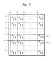
- FIG. 9 is a view showing pixels applied with the second left-eye data voltage FLV and the second right-eye data voltage FRV, according to an exemplary embodiment of the present invention.
- the pixels may include a third pixel PXL 3 connected to the i-th gate line Gi and a fourth pixel PXL 4 connected to the (i+1)th gate line Gi+1.
- the third pixel PXL 3 may be applied with one of the second left-eye row voltages LDV 1 to LDVn ⁇ 1 or one of the second right-eye row voltages RDV 1 to RDVn ⁇ 1.
- the fourth pixel PXL 4 may be applied with one of the left-eye compensation voltages LDV′ 1 to LDV′n ⁇ 1 or one of the right-eye compensation voltages RDV′ 1 to RDV′n ⁇ 1.
- the i-th second gate signal applied to the i-th gate line Gi and the (i+1)th second gate signal applied to the (i+1)th gate line Gi+1 have different ON-time periods from each other.
- the third pixel PXL 3 and the fourth pixel PXL 4 are applied with different data voltages from each other.
- the display quality of the stereoscopic image display system 10 may be prevented from being deteriorated and the stereoscopic image display system 10 may display vivid 3D images even though the data signal input to the timing controller 300 has half the resolution of the 3D image signal. This may be achieved by the scaling process performed by the timing controller 300 .
- the driving time of the pixels, which are respectively connected to the i-th gate line Gi and the (i+1)th gate line Gi+1 among the gate lines G 1 to Gk and to the same data line among the data lines D 1 to Dm, in the first mode M 1 may be the same as the driving time of the pixels in the second mode M 2 .
- the first gate signal having the pulse width of about ( 1/60) ⁇ (1/k) second is substantially simultaneously applied to the first and second pixels PXL 1 and PXL 2 .
- the second gate signal having the pulse width of about ( 1/120) ⁇ (1/k) second is sequentially applied to the third and fourth pixels PXL 3 and PXL 4 .
- the driving time of the two pixels in the first mode M 1 may be the same as the driving time of the two pixels in the second mode M 2 , e.g., ( 1/60) ⁇ (1/k).
- the data driver 400 and the gate driver 500 has the driving frequency of about 60 Hz or about 120 Hz
- the stereoscopic image display system 10 is operated at the frequency of about 120 Hz to display the 3D image.
- FIG. 10 is a block diagram showing a stereoscopic image display apparatus according to an exemplary embodiment of the present invention.
- a display apparatus 30 includes a display panel 100 , a data driver 400 , a gate driver 500 , and a timing controller 1000 .
- the data driver 400 and the gate driver 500 shown in FIG. 10 have the same structure and function as those of the stereoscopic image display system 10 shown in FIG. 1 , and thus detailed descriptions of the data driver 400 and the gate driver 500 will be omitted.
- the timing controller 1000 will be described in detail.
- the timing controller 1000 may include a 3D image signal generator 1100 .
- the stereoscopic image display system 10 shown in FIG. 1 includes the 3D image signal generator 200 separated from the display apparatus 20 , but the display apparatus 30 shown in FIG. 10 includes the 3D image signal generator 1100 is inside the timing controller 1000 .
- the 3D image signal generator 1100 may have the same configuration as the 3D image signal generator 200 shown in FIG. 2 .
- the timing controller 1000 (by way of the 3D image signal generator 1100 ) separates the image signal DATA from an external device (not shown) into the first left-eye frame data L 1 and the first right-eye frame data R 1 and down-scales the first left-eye frame data L 1 and the first right-eye frame data R 1 to generate the left-eye data L 1 / 2 and the right-eye data R 1 / 2 each having the half resolution.
- the timing controller 1000 sequentially applies the left-eye data L 1 / 2 and the right-eye data R 1 / 2 to the data driver 400 during the first mode M 1 .
- the timing controller 1000 generates the second left-eye frame data L 2 and the second right-eye frame data R 2 using the left-eye data L 1 / 2 and the right-eye data R 1 / 2 and applies the second left-eye frame data L 2 and the second right-eye frame data R 2 to the data driver 400 .
- the data driver 400 and the gate driver 500 perform the above-mentioned processes.
- a stereoscopic image display system may display a 3D image using the data and gate drivers each having the driving frequency of about 60 Hz.
- the stereoscopic image display system may display the 3D image even though the data and gate drivers have the driving frequency of about 60 Hz or about 120 Hz.
- the stereoscopic image display system may display the 3D image without using a frame memory for storing the left-eye frame data or the right-eye frame data when the left-eye frame data or the right-eye frame data, which are input to the display apparatus, has the frequency of about 60 Hz.
Abstract
Description
Claims (21)
Applications Claiming Priority (2)
| Application Number | Priority Date | Filing Date | Title |
|---|---|---|---|
| KR10-2012-0012921 | 2012-02-08 | ||
| KR1020120012921A KR101928555B1 (en) | 2012-02-08 | 2012-02-08 | Stereoscopic image display apparatus and stereoscopic image display system comprising thereof |
Publications (2)
| Publication Number | Publication Date |
|---|---|
| US20130201181A1 US20130201181A1 (en) | 2013-08-08 |
| US9165529B2 true US9165529B2 (en) | 2015-10-20 |
Family
ID=48902482
Family Applications (1)
| Application Number | Title | Priority Date | Filing Date |
|---|---|---|---|
| US13/746,139 Expired - Fee Related US9165529B2 (en) | 2012-02-08 | 2013-01-21 | Stereoscopic image display apparatus and a stereoscopic image display system having the same |
Country Status (2)
| Country | Link |
|---|---|
| US (1) | US9165529B2 (en) |
| KR (1) | KR101928555B1 (en) |
Families Citing this family (4)
| Publication number | Priority date | Publication date | Assignee | Title |
|---|---|---|---|---|
| KR102241693B1 (en) | 2014-08-25 | 2021-04-20 | 삼성디스플레이 주식회사 | Organic light emitting display device and methode of driving the same |
| GB201602543D0 (en) * | 2016-02-12 | 2016-03-30 | Crystal Vision Ltd | Improvement seen and relating to video multiviewer systems |
| CN106851255B (en) | 2017-03-29 | 2018-09-14 | 京东方科技集团股份有限公司 | Stereoscopic display driving method, device and display equipment |
| KR102340929B1 (en) * | 2020-06-16 | 2021-12-17 | (주)디앤티 | 3D image processing method and apparatus |
Citations (18)
| Publication number | Priority date | Publication date | Assignee | Title |
|---|---|---|---|---|
| KR20000050024A (en) | 2000-05-12 | 2000-08-05 | 김성식 | stereo PMD(Personal Mobile Display) system using a single display device |
| KR20090046424A (en) | 2007-11-06 | 2009-05-11 | 현대자동차주식회사 | Radiator insulator for automobile |
| US20100060720A1 (en) * | 2008-09-09 | 2010-03-11 | Yasutaka Hirasawa | Apparatus, method, and computer program for analyzing image data |
| JP2010061105A (en) | 2008-08-07 | 2010-03-18 | Mitsubishi Electric Corp | Image display apparatus and method |
| KR20100042954A (en) | 2008-10-17 | 2010-04-27 | 엘지디스플레이 주식회사 | Image display device and driving method thereof |
| KR20100075206A (en) | 2008-12-24 | 2010-07-02 | 삼성전자주식회사 | Method and apparatus for displaying 2-dimensional image sequence or 3-dimensional image sequence with frame rate adjustment |
| JP2010528327A (en) | 2007-05-18 | 2010-08-19 | スリーエム イノベイティブ プロパティズ カンパニー | Stereoscopic 3D Liquid Crystal Display Device Using Black Data Insertion |
| US20100259511A1 (en) * | 2007-02-15 | 2010-10-14 | Kazunori Kimura | Display system, control system, and display method |
| KR20100128019A (en) | 2009-05-27 | 2010-12-07 | 엘지디스플레이 주식회사 | Image display device and driving method of thereof |
| KR20100139017A (en) | 2008-03-19 | 2010-12-31 | 쓰리엠 이노베이티브 프로퍼티즈 컴파니 | Autostereoscopic display with fresnel lens element |
| KR20110055196A (en) | 2009-11-19 | 2011-05-25 | 삼성전자주식회사 | Image displaying apparatus and image signal processing method of the same |
| US20110122126A1 (en) * | 2009-11-23 | 2011-05-26 | Samsung Electronics Co., Ltd. | Method for providing three-dimensional (3d) image, method for converting 3d message, graphical user interface (gui) providing method related to 3d image, and 3d display apparatus and system for providing 3d image |
| US20110129269A1 (en) | 2009-12-01 | 2011-06-02 | Kumiko Seo | Image forming apparatus and process cartridge |
| US20110128269A1 (en) | 2009-11-30 | 2011-06-02 | Lee Myounghwa | Steroscopic image display device and driving method thereof |
| KR20110062766A (en) | 2009-12-04 | 2011-06-10 | 엘지디스플레이 주식회사 | Frame rate control dithering circuit of video dispaly device and method thereof |
| US20110148860A1 (en) | 2009-12-23 | 2011-06-23 | Au Optronics Corp. | Stereoscopic display |
| WO2011145584A1 (en) * | 2010-05-17 | 2011-11-24 | シャープ株式会社 | Liquid-crystal display device |
| US20120249759A1 (en) * | 2011-03-31 | 2012-10-04 | Sony Corporation | 3-d controller system for legacy tv |
Family Cites Families (3)
| Publication number | Priority date | Publication date | Assignee | Title |
|---|---|---|---|---|
| KR20050079385A (en) * | 2004-02-05 | 2005-08-10 | 삼성전자주식회사 | Method for transmitting/receiving of signal, display device for performing the same, and apparatus and method for driving thereof |
| KR20080064514A (en) * | 2007-01-05 | 2008-07-09 | 삼성전자주식회사 | Display apparatus for processing 3d image signal and control method thereof |
| KR101328808B1 (en) * | 2010-05-13 | 2013-11-13 | 엘지디스플레이 주식회사 | Image display device |
-
2012
- 2012-02-08 KR KR1020120012921A patent/KR101928555B1/en active IP Right Grant
-
2013
- 2013-01-21 US US13/746,139 patent/US9165529B2/en not_active Expired - Fee Related
Patent Citations (19)
| Publication number | Priority date | Publication date | Assignee | Title |
|---|---|---|---|---|
| KR20000050024A (en) | 2000-05-12 | 2000-08-05 | 김성식 | stereo PMD(Personal Mobile Display) system using a single display device |
| US20100259511A1 (en) * | 2007-02-15 | 2010-10-14 | Kazunori Kimura | Display system, control system, and display method |
| JP2010528327A (en) | 2007-05-18 | 2010-08-19 | スリーエム イノベイティブ プロパティズ カンパニー | Stereoscopic 3D Liquid Crystal Display Device Using Black Data Insertion |
| KR20090046424A (en) | 2007-11-06 | 2009-05-11 | 현대자동차주식회사 | Radiator insulator for automobile |
| KR20100139017A (en) | 2008-03-19 | 2010-12-31 | 쓰리엠 이노베이티브 프로퍼티즈 컴파니 | Autostereoscopic display with fresnel lens element |
| JP2010061105A (en) | 2008-08-07 | 2010-03-18 | Mitsubishi Electric Corp | Image display apparatus and method |
| US20100060720A1 (en) * | 2008-09-09 | 2010-03-11 | Yasutaka Hirasawa | Apparatus, method, and computer program for analyzing image data |
| KR20100042954A (en) | 2008-10-17 | 2010-04-27 | 엘지디스플레이 주식회사 | Image display device and driving method thereof |
| KR20100075206A (en) | 2008-12-24 | 2010-07-02 | 삼성전자주식회사 | Method and apparatus for displaying 2-dimensional image sequence or 3-dimensional image sequence with frame rate adjustment |
| KR20100128019A (en) | 2009-05-27 | 2010-12-07 | 엘지디스플레이 주식회사 | Image display device and driving method of thereof |
| KR20110055196A (en) | 2009-11-19 | 2011-05-25 | 삼성전자주식회사 | Image displaying apparatus and image signal processing method of the same |
| US20110122126A1 (en) * | 2009-11-23 | 2011-05-26 | Samsung Electronics Co., Ltd. | Method for providing three-dimensional (3d) image, method for converting 3d message, graphical user interface (gui) providing method related to 3d image, and 3d display apparatus and system for providing 3d image |
| US20110128269A1 (en) | 2009-11-30 | 2011-06-02 | Lee Myounghwa | Steroscopic image display device and driving method thereof |
| US20110129269A1 (en) | 2009-12-01 | 2011-06-02 | Kumiko Seo | Image forming apparatus and process cartridge |
| KR20110062766A (en) | 2009-12-04 | 2011-06-10 | 엘지디스플레이 주식회사 | Frame rate control dithering circuit of video dispaly device and method thereof |
| US20110148860A1 (en) | 2009-12-23 | 2011-06-23 | Au Optronics Corp. | Stereoscopic display |
| WO2011145584A1 (en) * | 2010-05-17 | 2011-11-24 | シャープ株式会社 | Liquid-crystal display device |
| US20130057791A1 (en) * | 2010-05-17 | 2013-03-07 | Sharp Kabushiki Kaisha | Liquid-crystal display device |
| US20120249759A1 (en) * | 2011-03-31 | 2012-10-04 | Sony Corporation | 3-d controller system for legacy tv |
Also Published As
| Publication number | Publication date |
|---|---|
| KR20130091546A (en) | 2013-08-19 |
| US20130201181A1 (en) | 2013-08-08 |
| KR101928555B1 (en) | 2018-12-14 |
Similar Documents
| Publication | Publication Date | Title |
|---|---|---|
| TWI693583B (en) | Display device and driving method thereof | |
| CN105719592B (en) | Display device and driving method thereof | |
| US9330617B2 (en) | Method of driving a display panel and display apparatus for performing the same | |
| KR101876848B1 (en) | 2D/3D switchable image display apparatus and method of displaying 2D/3D image | |
| JP5367063B2 (en) | 3D display device driving method and 3D display device | |
| KR101685590B1 (en) | Three dimensional image display device | |
| US9196184B2 (en) | Method of driving display panel and display apparatus for performing the same | |
| US20120162172A1 (en) | Method of driving display panel and display apparatus performing the method | |
| US9542899B2 (en) | Method of driving display panel, display panel driving apparatus for performing the method and display apparatus having the display panel driving apparatus | |
| US9204137B2 (en) | Timing control unit and apparatus and method for displaying using the same | |
| US9165529B2 (en) | Stereoscopic image display apparatus and a stereoscopic image display system having the same | |
| US20130342513A1 (en) | Display apparatus and method of driving the display apparatus | |
| US9088788B2 (en) | Method of displaying a three dimensional image and display apparatus for performing the method | |
| US20120139905A1 (en) | Stereoscopic image display device and driving method thereof | |
| US8872989B2 (en) | Electro-optical device and electronic apparatus | |
| US9615077B2 (en) | Display apparatus and a method of driving the same | |
| KR101221611B1 (en) | Stereoscopic image display device, and driving method the same | |
| US20110216174A1 (en) | Method for displaying stereoscopic images |
Legal Events
| Date | Code | Title | Description |
|---|---|---|---|
| AS | Assignment |
Owner name: SAMSUNG DISPLAY CO., LTD., KOREA, REPUBLIC OF Free format text: ASSIGNMENT OF ASSIGNORS INTEREST;ASSIGNORS:LEE, JUNPYO;MOON, HOISIK;NAM, GWANGHO;AND OTHERS;REEL/FRAME:029664/0500 Effective date: 20121211 |
|
| STCF | Information on status: patent grant |
Free format text: PATENTED CASE |
|
| FEPP | Fee payment procedure |
Free format text: PAYOR NUMBER ASSIGNED (ORIGINAL EVENT CODE: ASPN); ENTITY STATUS OF PATENT OWNER: LARGE ENTITY |
|
| MAFP | Maintenance fee payment |
Free format text: PAYMENT OF MAINTENANCE FEE, 4TH YEAR, LARGE ENTITY (ORIGINAL EVENT CODE: M1551); ENTITY STATUS OF PATENT OWNER: LARGE ENTITY Year of fee payment: 4 |
|
| FEPP | Fee payment procedure |
Free format text: MAINTENANCE FEE REMINDER MAILED (ORIGINAL EVENT CODE: REM.); ENTITY STATUS OF PATENT OWNER: LARGE ENTITY |
|
| LAPS | Lapse for failure to pay maintenance fees |
Free format text: PATENT EXPIRED FOR FAILURE TO PAY MAINTENANCE FEES (ORIGINAL EVENT CODE: EXP.); ENTITY STATUS OF PATENT OWNER: LARGE ENTITY |
|
| STCH | Information on status: patent discontinuation |
Free format text: PATENT EXPIRED DUE TO NONPAYMENT OF MAINTENANCE FEES UNDER 37 CFR 1.362 |
|
| FP | Lapsed due to failure to pay maintenance fee |
Effective date: 20231020 |